
Nanoelectromechanical Temperature Sensor Based on Piezoresistive Properties of Suspended Graphene Film

 ,
,  , , and
Abstract
:1. Introduction
2. Materials and Methods
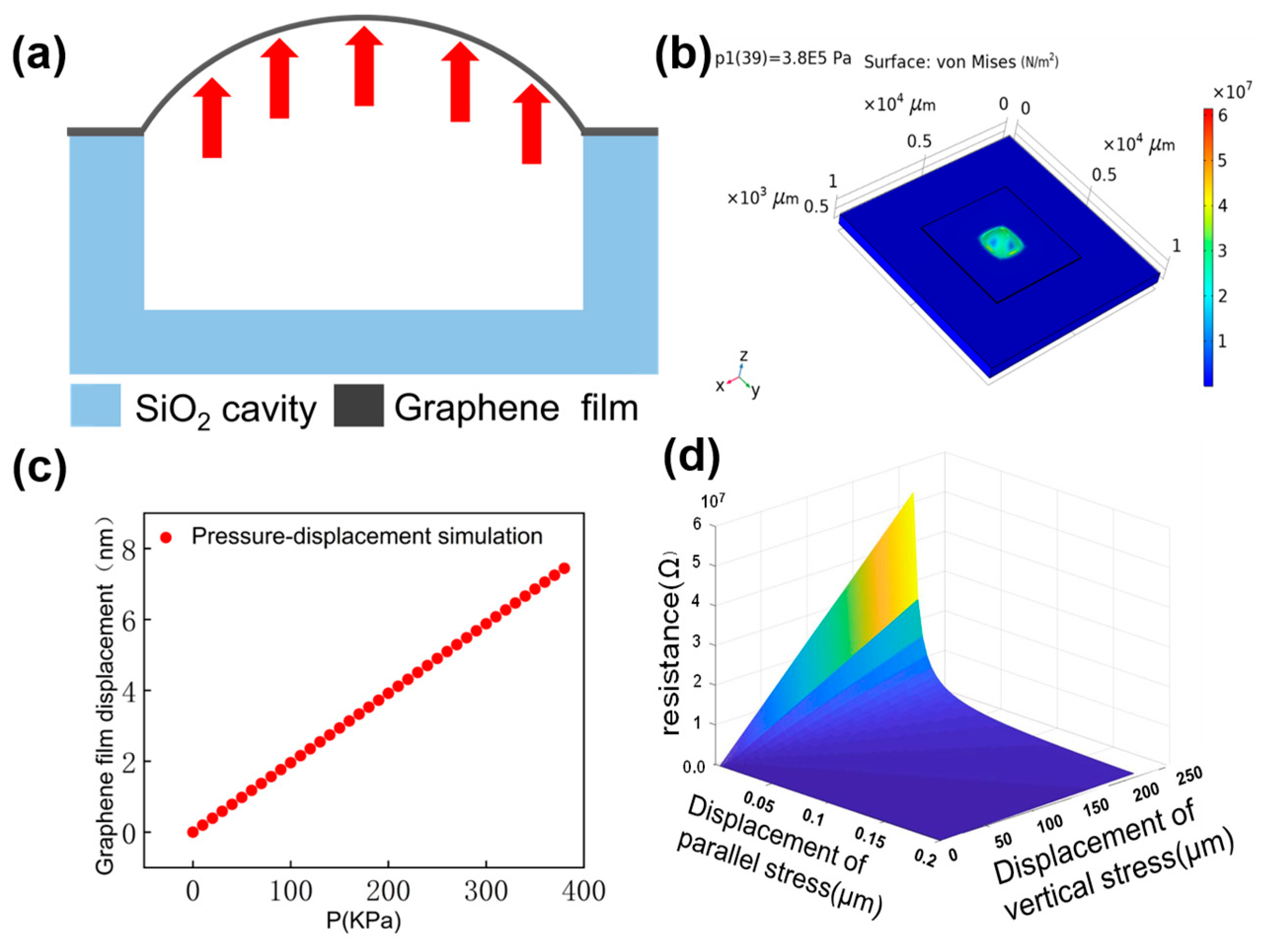
2.1. Simulation
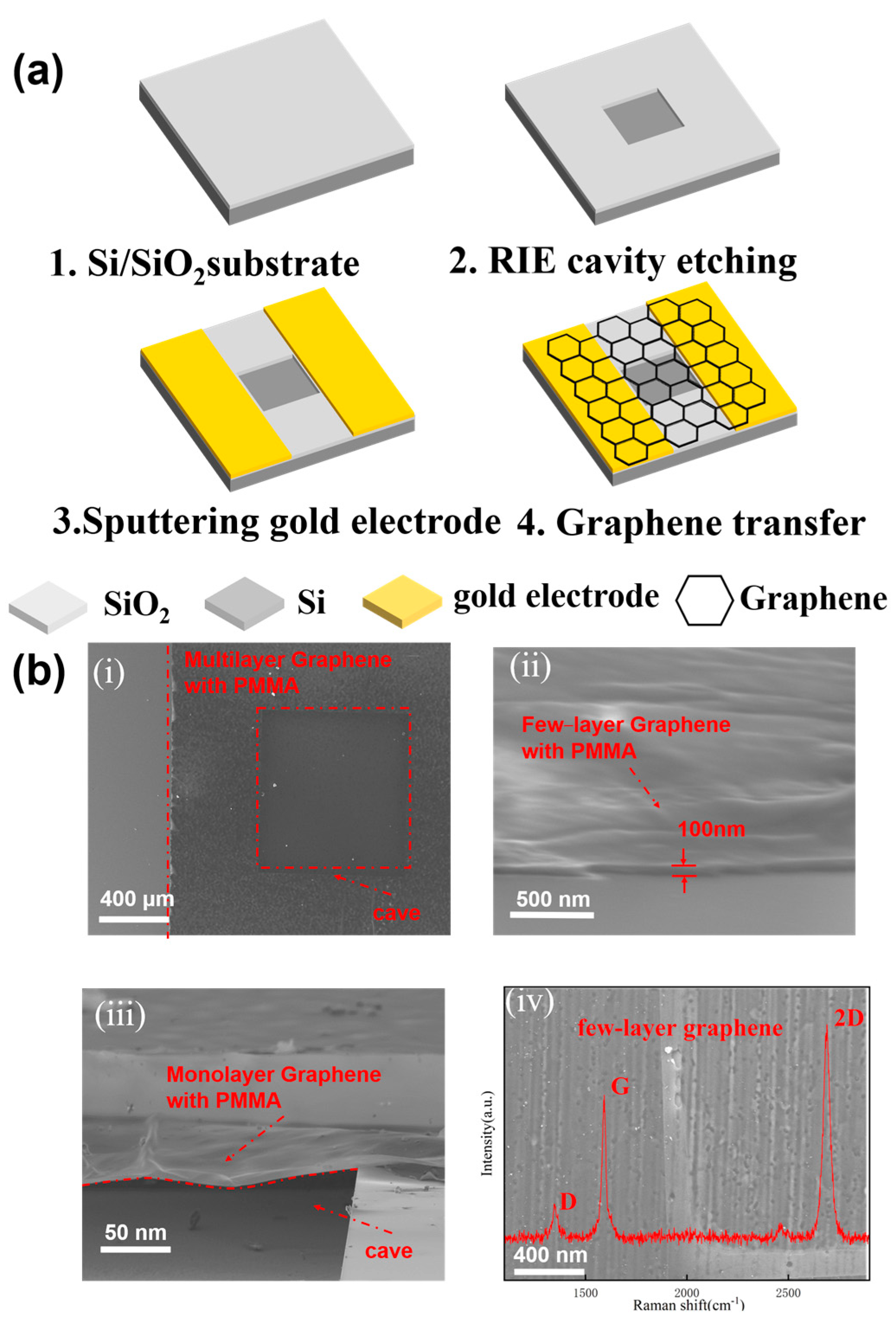
2.2. Experiments
Device Fabrication
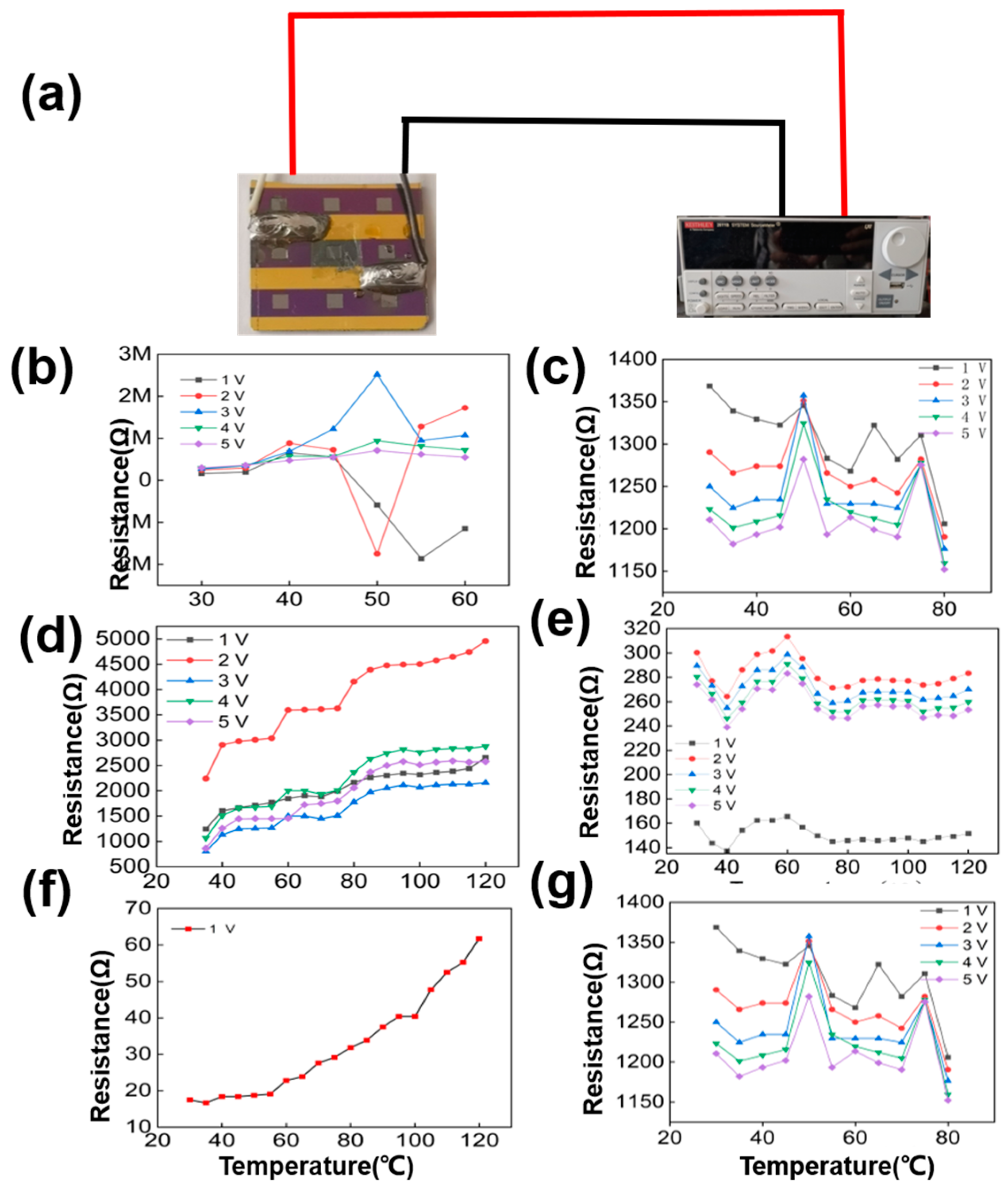
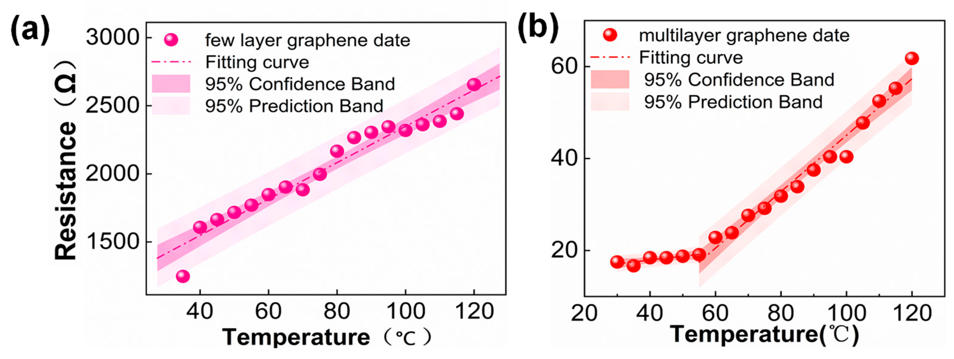
3. Results
4. Discussion
5. Conclusions
Author Contributions
Funding
Data Availability Statement
Conflicts of Interest
References
- Yan, C.; Wang, J.; Lee, P.S. Stretchable graphene thermistor with tunable thermal index. ACS Nano 2015, 9, 2130–2137. [Google Scholar] [CrossRef] [PubMed]
- Zheng, Q.; Lee, J.-h.; Shen, X.; Chen, X.; Kim, J.-K. Graphene-based wearable piezoresistive physical sensors. Mater. Today 2020, 36, 158–179. [Google Scholar] [CrossRef]
- Tung, T.T.; Pham-Huu, C.; Janowska, I.; Kim, T.; Castro, M.; Feller, J.-F. Hybrid Films of Graphene and Carbon Nanotubes for High Performance Chemical and Temperature Sensing Applications. Small 2015, 11, 3485–3493. [Google Scholar] [CrossRef] [PubMed]
- Nag, A.; Simorangkir, R.B.V.B.; Gawade, D.R.; Nuthalapati, S.; Buckley, J.L.; O’Flynn, B.; Altinsoy, M.E.; Mukhopadhyay, S.C. Graphene-based wearable temperature sensors: A review. Mater. Des. 2022, 221, 110971. [Google Scholar] [CrossRef]
- Akinwande, D.; Brennan, C.J.; Bunch, J.S.; Egberts, P.; Felts, J.R.; Gao, H.; Huang, R.; Kim, J.-S.; Li, T.; Li, Y.; et al. A review on mechanics and mechanical properties of 2D materials—Graphene and beyond. Extrem. Mech. Lett. 2017, 13, 42–77. [Google Scholar] [CrossRef] [Green Version]
- Liu, Y.; Tao, L.Q.; Wang, D.Y.; Zhang, T.Y.; Yang, Y.; Ren, T.L. Flexible, highly sensitive pressure sensor with a wide range based on graphene-silk network structure. Appl. Phys. Lett. 2017, 110, 123508. [Google Scholar] [CrossRef]
- Liu, G.; Tan, Q.; Kou, H.; Zhang, L.; Wang, J.; Lv, W.; Dong, H.; Xiong, J. A Flexible Temperature Sensor Based on Reduced Graphene Oxide for Robot Skin Used in Internet of Things. Sensors 2018, 18, 1400. [Google Scholar] [CrossRef] [Green Version]
- Wagner, S.; Weisenstein, C.; Smith, A.D.; Ostling, M.; Kataria, S.; Lemme, M.C. Graphene transfer methods for the fabrication of membrane-based NEMS devices. Microelectron. Eng. 2016, 159, 108–113. [Google Scholar] [CrossRef]
- Zhang, Y.; Tan, Y.W.; Stormer, H.L.; Kim, P. Experimental observation of the quantum Hall effect and Berry’s phase in graphene. Nature 2005, 438, 201–204. [Google Scholar] [CrossRef] [PubMed] [Green Version]
- Stankovich, S.; Dikin, D.A.; Dommett, G.H.B.; Kohlhaas, K.M.; Zimney, E.J.; Stach, E.A.; Piner, R.D.; Nguyen, S.T.; Ruoff, R.S. Graphene-based composite materials. Nature 2006, 442, 282–286. [Google Scholar] [CrossRef]
- Sahatiya, P.; Puttapati, S.K.; Srikanth, V.V.S.S.; Badhulika, S. Graphene-based wearable temperature sensor and infrared photodetector on a flexible polyimide substrate. Flex. Print. Electron. 2016, 1, 10. [Google Scholar] [CrossRef]
- Kaur, A.; Singh, R.C. Temperature sensor based on exfoliated graphene sheets produced by microwave assisted freezing induced volumetric expansion of carbonated water. J. Mater. Sci. Mater. Electron. 2019, 30, 5791–5807. [Google Scholar] [CrossRef]
- Worsley, M.A.; Pauzauskie, P.J.; Olson, T.Y.; Biener, J.; Satcher, J.H.; Baumann, T.F. Synthesis of Graphene Aerogel with High Electrical Conductivity. J. Am. Chem. Soc. 2010, 132, 14067–14069. [Google Scholar] [CrossRef] [PubMed]
- Jeong, H.Y.; Lee, D.S.; Choi, H.K.; Lee, D.H.; Kim, J.E.; Lee, J.Y.; Lee, W.J.; Kim, S.O.; Choi, S.Y. Flexible room-temperature NO2 gas sensors based on carbon nanotubes/reduced graphene hybrid films. Appl. Phys. Lett. 2010, 96, 213105. [Google Scholar] [CrossRef] [Green Version]
- Ricciardella, F.; Massera, E.; Polichetti, T.; Miglietta, M.L.; Di Francia, G. A calibrated graphene-based chemi-sensor for sub parts-per-million NO2 detection operating at room temperature. Appl. Phys. Lett. 2014, 104, 183502. [Google Scholar] [CrossRef]
- Ke, F.; Song, F.; Zhang, H.; Xu, J.; Wang, H.; Chen, Y. Layer-by-layer assembly for all-graphene coated conductive fibers toward superior temperature sensitivity and humidity independence. Compos. Part B Eng. 2020, 200, 108253. [Google Scholar] [CrossRef]
- Zhang, J.; Liao, G.; Jin, S.; Cao, D.; Wei, Q.; Lu, H.; Yu, J.; Cai, X.; Tan, S.; Xiao, Y.; et al. All-fiber-optic temperature sensor based on reduced graphene oxide. Laser Phys. Lett. 2014, 11, 035901. [Google Scholar] [CrossRef]
- Chu, R.; Guan, C.; Bo, Y.; Shi, J.; Zhu, Z.; Li, P.; Yang, J.; Yuan, L. Temperature Sensor in Suspended Core Hollow Fiber Covered With Reduced Graphene Oxide. IEEE Photonics Technol. Lett. 2019, 31, 553–556. [Google Scholar] [CrossRef]
- Saafi, M.; Piukovics, G.; Ye, J. Hybrid graphene/geopolymeric cement as a superionic conductor for structural health monitoring applications. Smart Mater. Struct. 2016, 25, 105018. [Google Scholar] [CrossRef]
- Quang, V.V.; Dung, N.V.; Trong, N.S.; Hoa, N.D.; Duy, N.V.; Hieu, N.V. Outstanding gas-sensing performance of graphene/SnO2 nanowire Schottky junctions. Appl. Phys. Lett. 2014, 105, 013107. [Google Scholar] [CrossRef]
- Mu, H.C.; Zhang, Z.Q.; Zhao, X.J.; Liu, F.; Wang, K.K.; Xie, H.F. High sensitive formaldehyde graphene gas sensor modified by atomic layer deposition zinc oxide films. Appl. Phys. Lett. 2014, 105, 033107. [Google Scholar] [CrossRef]
- Mohammad Haniff, M.A.; Muhammad Hafiz, S.; Wahid, K.A.; Endut, Z.; Wah Lee, H.; Bien, D.C.; Abdul Azid, I.; Abdullah, M.Z.; Ming Huang, N.; Abdul Rahman, S. Piezoresistive effects in controllable defective HFTCVD graphene-based flexible pressure sensor. Sci. Rep. 2015, 5, 14751. [Google Scholar] [CrossRef] [Green Version]
- Davaji, B.; Cho, H.D.; Malakoutian, M.; Lee, J.K.; Panin, G.; Kang, T.W.; Lee, C.H. A patterned single layer graphene resistance temperature sensor. Sci. Rep. 2017, 7, 8811. [Google Scholar] [CrossRef]
- Sun, P.; Zhu, M.; Wang, K.; Zhong, M.; Wei, J.; Wu, D.; Zhu, H. Small temperature coefficient of resistivity of graphene/graphene oxide hybrid membranes. ACS Appl. Mater. Interfaces 2013, 5, 9563–9571. [Google Scholar] [CrossRef] [PubMed]
- Chen, C.; Rosenblatt, S.; Bolotin, K.I.; Kalb, W.; Kim, P.; Kymissis, I.; Stormer, H.L.; Heinz, T.F.; Hone, J. Performance of monolayer graphene nanomechanical resonators with electrical readout. Nat. Nanotechnol. 2009, 4, 861–867. [Google Scholar] [CrossRef] [PubMed] [Green Version]
- Yang, H.; Paek, K.; Kim, B.J. Efficient temperature sensing platform based on fluorescent block copolymer-functionalized graphene oxide. Nanoscale 2013, 5, 5720–5724. [Google Scholar] [CrossRef]
- Urban, F.; Lupina, G.; Grillo, A.; Martucciello, N.; Di Bartolomeo, A. Contact resistance and mobility in back-gate graphene transistors. Nano Express 2020, 1, 010001. [Google Scholar] [CrossRef]
- Bolotin, K.I.; Sikes, K.J.; Jiang, Z.; Klima, M.; Fudenberg, G.; Hone, J.; Kim, P.; Stormer, H.L. Ultrahigh electron mobility in suspended graphene. Solid State Commun. 2008, 146, 351–355. [Google Scholar] [CrossRef] [Green Version]
- Vaquero, D.; Clerico, V.; Schmitz, M.; Delgado-Notario, J.A.; Martin-Ramos, A.; Salvador-Sanchez, J.; Muller, C.S.A.; Rubi, K.; Watanabe, K.; Taniguchi, T. Phonon-mediated room-temperature quantum Hall transport in graphene. Nat. Commun. 2023, 14, 318. [Google Scholar] [CrossRef] [PubMed]
- Chen, J.H.; Jang, C.; Xiao, S.; Ishigami, M.; Fuhrer, M.S. Intrinsic and extrinsic performance limits of graphene devices on SiO2. Nat. Nanotechnol. 2008, 3, 206–209. [Google Scholar] [CrossRef]
- Smith, A.D.; Niklaus, F.; Paussa, A.; Vaziri, S.; Fischer, A.C.; Sterner, M.; Forsberg, F.; Delin, A.; Esseni, D.; Palestri, P.; et al. Electromechanical piezoresistive sensing in suspended graphene membranes. Nano Lett. 2013, 13, 3237–3242. [Google Scholar] [CrossRef]
- Yu, J.B.; Xian, S.; Zhang, Z.P.; Hou, X.J.; He, J.; Mu, J.L.; Geng, W.P.; Qiao, X.J.; Zhang, L.; Chou, X.J. Synergistic piezoelectricity enhanced BaTiO3/polyacrylonitrile elastomer-based highly sensitive pressure sensor for intelligent sensing and posture recognition applications. Nano Res. 2022. [Google Scholar] [CrossRef]
- Smith, A.D.; Niklaus, F.; Paussa, A.; Schroder, S.; Fischer, A.C.; Sterner, M.; Wagner, S.; Vaziri, S.; Forsberg, F.; Esseni, D.; et al. Piezoresistive Properties of Suspended Graphene Membranes under Uniaxial and Biaxial Strain in Nanoelectromechanical Pressure Sensors. ACS Nano 2016, 10, 9879–9886. [Google Scholar] [CrossRef] [PubMed] [Green Version]
- Tomori, H.; Kanda, A.; Goto, H.; Ootuka, Y.; Tsukagoshi, K.; Moriyama, S.; Watanabe, E.; Tsuya, D. Introducing Nonuniform Strain to Graphene Using Dielectric Nanopillars. Appl. Phys. Express 2011, 4, 075102. [Google Scholar] [CrossRef] [Green Version]
- Koenig, S.P.; Boddeti, N.G.; Dunn, M.L.; Bunch, J.S. Ultrastrong adhesion of graphene membranes. Nat. Nanotechnol. 2011, 6, 543–546. [Google Scholar] [CrossRef] [Green Version]
- Tao, J.; Wang, X.H.; Wang, Z.D.; Zeng, Q. Graphene nanoplatelets as an effective additive to tune the microstructures and piezoresistive properties of cement-based composites. Constr. Build. Mater. 2019, 209, 665–678. [Google Scholar] [CrossRef]
- Jorudas, J.; Pashnev, D.; Kasalynas, I.; Ignatjev, I.; Niaura, G.; Selskis, A.; Astachov, V.; Alexeeva, N. Green Removal of DUV-Polarity-Modified PMMA for Wet Transfer of CVD Graphene. Nanomaterials 2022, 12, 4017. [Google Scholar] [CrossRef] [PubMed]
- Gholami, Z.; Khoeini, F. Pure thermal spin current and perfect spin-filtering with negative differential thermoelectric resistance induced by proximity effect in graphene/silicene junctions. Sci. Rep. 2021, 11, 104. [Google Scholar] [CrossRef]
- Liu, H.T.; Liu, Y.Q.; Zhu, D.B. Chemical doping of graphene. J. Mater. Chem. 2011, 21, 3335–3345. [Google Scholar] [CrossRef]
- Chen, J.H.; Jang, C.; Adam, S.; Fuhrer, M.S.; Williams, E.D.; Ishigami, M. Charged-impurity scattering in graphene. Nat. Phys. 2008, 4, 377–381. [Google Scholar] [CrossRef] [Green Version]
- Karimov, K.S.; Chani, M.T.S.; Khalid, F.A. Carbon nanotubes film based temperature sensors. Phys. E Low-Dimens. Syst. Nanostruct. 2011, 43, 1701–1703. [Google Scholar] [CrossRef]
- Rajan, G.; Morgan, J.J.; Murphy, C.; Torres Alonso, E.; Wade, J.; Ott, A.K.; Russo, S.; Alves, H.; Craciun, M.F.; Neves, A.I.S. Low Operating Voltage Carbon-Graphene Hybrid E-textile for Temperature Sensing. ACS Appl. Mater. Interfaces 2020, 12, 29861–29867. [Google Scholar] [CrossRef] [PubMed]
- Ali, K.; Hafez, M. Growth and structure of carbon nanotubes based novel catalyst for ultrafast nano-temperature sensor application. Superlattices Microstruct. 2013, 54, 1–6. [Google Scholar] [CrossRef]


| Material | Operating Rang | TCR * |
|---|---|---|
| BN/Gra/BN [23] | 30–150 °C | 0.25%/°C |
| Monologue Gra [21] | 9–29 °C | −0.16%/°C |
| Muti-walled CNTs [31] | −33–126 °C | −0.13%/°C |
| Graphene, PP texti [32] | 30–70 °C | −0.17%/°C |
| CNTs prepared by CVD [33] | 30–150 °C | 0.04%/°C |
| Multilayer Gra (This work) | 25–120 °C | 3.50%/°C |
Disclaimer/Publisher’s Note: The statements, opinions and data contained in all publications are solely those of the individual author(s) and contributor(s) and not of MDPI and/or the editor(s). MDPI and/or the editor(s) disclaim responsibility for any injury to people or property resulting from any ideas, methods, instructions or products referred to in the content. |
© 2023 by the authors. Licensee MDPI, Basel, Switzerland. This article is an open access article distributed under the terms and conditions of the Creative Commons Attribution (CC BY) license (https://creativecommons.org/licenses/by/4.0/).
Share and Cite
Han, S.; Zhou, S.; Mei, L.; Guo, M.; Zhang, H.; Li, Q.; Zhang, S.; Niu, Y.; Zhuang, Y.; Geng, W.; et al. Nanoelectromechanical Temperature Sensor Based on Piezoresistive Properties of Suspended Graphene Film. Nanomaterials 2023, 13, 1103. https://doi.org/10.3390/nano13061103
Han S, Zhou S, Mei L, Guo M, Zhang H, Li Q, Zhang S, Niu Y, Zhuang Y, Geng W, et al. Nanoelectromechanical Temperature Sensor Based on Piezoresistive Properties of Suspended Graphene Film. Nanomaterials. 2023; 13(6):1103. https://doi.org/10.3390/nano13061103
Chicago/Turabian StyleHan, Shuqi, Siyuan Zhou, Linyu Mei, Miaoli Guo, Huiyi Zhang, Qiannan Li, Shuai Zhang, Yaokai Niu, Yan Zhuang, Wenping Geng, and et al. 2023. "Nanoelectromechanical Temperature Sensor Based on Piezoresistive Properties of Suspended Graphene Film" Nanomaterials 13, no. 6: 1103. https://doi.org/10.3390/nano13061103