Design and simulation of a new QCA-based low-power universal gate
 Hamidreza Sadrarhami
 S. Mohammadali Zanjani3,4*
 - 1Faculty of Computer Engineering, Najafabad Branch, Islamic Azad University, Najafabad, Iran
- 2Big Data Research Center- Najafabad Branch, Islamic Azad University, Najafabad, Iran
- 3Department of Electrical Engineering- Najafabad Branch, Islamic Azad University, Najafabad, Iran
- 4Smart Microgrid Research Center- Najafabad Branch, Islamic Azad University, Najafabad, Iran
Quantum-dot Cellular Automata (QCA) is recognized in electronics for its low power consumption and high-density capabilities, emerging as a potential substitute for CMOS technology. GDI (Gate Diffusion Input) technology is featured as an innovative approach for enhancing power efficiency and spatial optimization in digital circuits. This study introduces an advanced four-input Improved Gate Diffusion Input (IGDI) design specifically for QCA technology as a universal gate. A key feature of the proposed 10-cell block is the absence of cross-wiring, which significantly enhances the circuit’s operational efficiency. Its universal cell nature allows for the carrying out of various logical gates by merely altering input values, without necessitating any structural redesign. The proposed design showcases notable advancements over prior models, including a reduced cell count by 17%, a 29% decrease in total energy usage, and a 44% reduction in average energy loss. This innovative IGDI design efficiently executes 21 combinational and various sequential functions. Simulations in 18 nm technology, accompanied by energy consumption analyses, demonstrate this design’s superior performance compared to existing models in key areas such as multiplexers, comparators, and memory circuits, alongside a significant reduction in cell count.
1 Introduction
The enhancement of system capabilities and the trend toward reduced hardware sizes have brought to light significant challenges in complementary metal-oxide-semiconductor (CMOS) technology, particularly with the shift toward nanoscale circuitry. This development has prompted an increased need for alternative technological solutions, focusing on enhancing power efficiency and reducing the size of circuits (Sadrarhami et al., 2018).
Quantum-dot Cellular Automata (QCA) has garnered interest as a potential alternative to CMOS technology, primarily due to its high circuit density (approximately 1,012 cells/cm2) and swift switching frequency (around 1 THz) (Naz et al., 2021). QCA technology uniquely integrates Boolean logic operations with quantum dot functionalities, leveraging the advanced physical simulation of both automata and quantum dot cells (Wang and Xie, 2018). This integration signifies a substantial advancement, aiming to enhance the efficiency and scalability of semiconductor technologies. A Quantum cell contains four quantum dots and two mobile electrons. The arrangement of these electrons along one of the two primary diagonals determines the logical value of the cell, either zero or one. This configuration relies on the Coulombic interactions among the electrons, not only with adjacent neighbors but also with cells in diagonal positions and those in different layers. Thus, the logical state of any given cell depends on the states of surrounding cells, highlighting the importance of a comprehensive evaluation of neighboring cell states for accurate charge determination (Mohammadi and Navi, 2018; Wang and Xie, 2018). Thus, the logical charge assigned to any given cell is linked to the charges of its surrounding cells, necessitating a comprehensive assessment of neighboring cell states to ascertain each cell’s charge (Wang and Xie, 2018) accurately. Figure 1 depicts a quantum cell in two polarization states of 0 and 1.
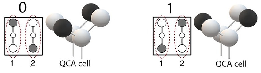
Figure 1. Two different polarization states of a QCA cell.
As illustrated in Figure 2, the architecture within QCA is segmented into four distinct clock zones, labeled 0, 1, 2, and 3. Each zone is characterized by a unique sequence of four clock phases: switch, hold, release, and relax (Sadeghi et al., 2020).at the switch phase, the cell’s polarization state is established. Following this, the hold phase maintains this specified polarization without alteration. Progressing to the release phase, there is a gradual diminishment in the cell’s polarization, leading to the relax phase where the cell’s polarization is entirely neutralized. This cycle ensures precise control over the cell’s energy state and data flow, highlighting the intricate design and operational efficacy inherent in QCA technology (Abutaleb, 2018).
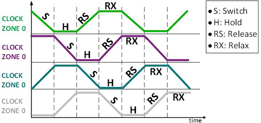
Figure 2. Four different phases in each clock zone (Sadeghi et al., 2020).
In the realm of dynamic circuit analysis, the evaluation of energy levels and the determination of cell polarization are crucial. This is achieved through simulations conducted with a correlation vector engine. Specifically, the kink energy concept is pivotal, reflecting the energy differential between cells a and b when they exhibit opposing polarizations. This energy differential is quantifiable through the electrostatic interactions analysis among the charges present (Cardenas-Barrera et al., 2002). The method involves a detailed computation of electrostatic interactions between disparate points within the same cell, guided by equation (1), wherein the proportionality constant, known as Coulomb’s constant, plays a fundamental role. The process to ascertain the kink energy entails an initial calculation of energy for cells exhibiting opposing polarities, followed by a similar computation for cells of identical polarity. The subtraction of these values yields the kink energy (Chen et al., 2019).
Circuit design errors in QCA technology encompass manufacturing, design, and clocking errors (Khan et al., 2023). Manufacturing errors, disrupt cell function due to chemical imperfections like single-electron defects (Bhat et al., 2023). The design errors affect both reversible and conventional circuits. Reversible design exhibits greater error resistance, maintaining functionality despite flaws and ensuring no data loss during computation. Although reversible design struggles with multiple lost or extra cell defects (Ahmadpour et al., 2023), common errors like cell displacement and wire crossing impact circuit function (Khan et al., 2023). Techniques such as the Friedkin gate, GDI gate, and tile design method have been utilized to mitigate these errors (Tougaw et al., 2021; Khan et al., 2023; Safaiezadeh et al., 2023). The tile in QCA technology, crucial for circuit design, provides higher error resistance than basic gates but may elevate circuit complexity. Optimal cell spacing for improved output ranges between 2 and 3 nanometers (Huang and Ottavi, 2005). In conventional design, QCA cells, majority gates, inverters, and wires form essential components, with errors in these elements leading to circuit flaws (Khan et al., 2023). Cell rotation is a notable error, particularly affecting curved QCA wires, with inverters exhibiting the least tolerance. Complex circuits are sensitive to rotation failures, but reliability can be enhanced by adding extra cells in the majority gate design. Cell misalignment poses additional challenges (Tougaw et al., 2021). The third type of fault is clocking errors. Accurate clocking, using appropriate methods, is vital for effectiveness. In QCA technology, clocking errors present a significant challenge that can affect the overall performance and reliability of computational circuits. Clocking in QCA is vital for controlling the information flow through the cells, ensuring that data moves in a precise and orderly manner (Khan et al., 2023). An error in the clocking sequence can disrupt this flow, leading to incorrect data processing and output. Such errors might occur due to synchronization issues, where the timing between different parts of the circuit becomes misaligned (Liu et al., 2014). Moreover, variations in fabrication processes can lead to inconsistencies in cell behavior under clocking signals, further exacerbating the problem. To mitigate clocking errors, designers employ rigorous simulation and testing methodologies, focusing on synchronization mechanisms and enhancing the robustness of the clocking architecture. This involves careful layout planning and the incorporation of error detection and correction mechanisms that can identify and compensate for clocking discrepancies, thereby ensuring that the circuit maintains its intended functionality even in the presence of potential clocking inaccuracies (Liu et al., 2014).
GDI as an innovative approach for digital circuits is primarily attributed to minimalist transistor requirement and its ability to minimize power dissipation compared to traditional CMOS technology (Sadrarhami et al., 2018). A basic GDI configuration involves the integration of one PMOS and one NMOS transistor (Ghorbani et al., 2022). The superiority of GDI over CMOS is evident through its reduced transistor count, accelerated operational speed, diminished power consumption, and the simplification of Boolean function implementations. Additionally, the strategic interconnection of multiple GDI cells facilitates the creation of complex multi-input gates. The basic structure of a GDI gate is shown in Figure 3. Table 1 illustrates different Boolean functions that can be generated using this block (Abiri et al., 2019). The GDI presents a notable approach for designing low-power and compact digital circuits, particularly useful in digital logic and microprocessor design. Despite its advantages in reducing power consumption, GDI faces challenges. The GDI technique might introduce challenges in achieving high-speed performance for certain applications, as the propagation delays inherent in GDI circuits could impact operational speed. Overcoming these challenges requires innovative design strategies and the integration of GDI with other technology such as QCA technology to balance power efficiency with performance and noise resilience (Abiri et al., 2019).
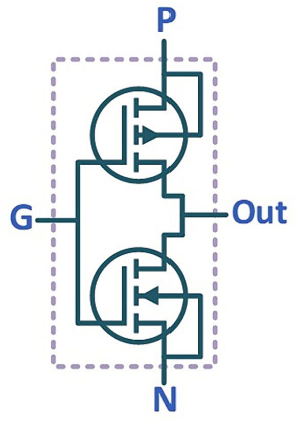
Figure 3. Gate diffusion input (Abiri et al., 2019).
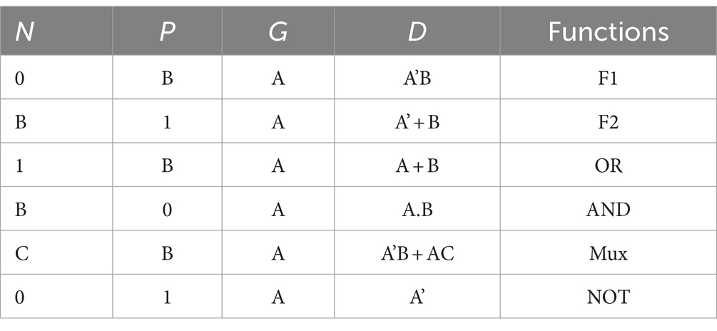
Table 1. Various logic functions for different input combinations of GDI cell (Abiri et al., 2019).
The typical approach to circuit design in QCA technology involves combining the majority gates and inverters, which tends to enlarge the circuit footprint. Additionally, establishing communication between different gates increases circuit latency. Introducing universal gates, particularly for complex circuitry, can reduce circuit size, latency, and power consumption (Riyaz et al., 2024).
Universal gates, offering a wider functionality spectrum compared to standard majority and inverter gates, hold promise for minimizing circuit size, power usage, and latency (Hayati and Rezaei, 2019). Optimization techniques often borrow from successful strategies in other technologies. Therefore, in addressing the design challenge in QCA technology, this paper proposes a versatile gate utilizing GDI optimized in QCA to perform various fundamental functions. This GDI’s application in QCA not only tackles GDI-related issues like high-speed performance, noise margins, and propagation delays but also resolves a fundamental challenge in QCA circuit design, namely the reliance on basic gates.
For instance, in reference (Ghorbani et al., 2022), a dynamic XOR cell and full adder design using a combination of GDI and dynamic logic, termed D-GDI, is proposed. This design reduces the area, Power Delay Product (PDP), and parasitic capacitances at the output node and intermediate nodes. The D-GDI full adder also shows a 20% reduction in power consumption compared to the best existing designs. An improved version of this cell in reference (Abiri et al., 2014) reduces the chip area for pull-up and pull-down networks by about 80 and 50%, respectively, compared to the basic GDI cell, while also improving the PDP.
However, GDI-based digital integrated circuits, while advantageous in terms of power efficiency and simplicity of design, face a limitation in achieving full-swing capability. To overcome this problem, dynamic logic has been integrated with GDI to enable full-swing functionality.
In Abiri et al. (2019), a GDI unit is proposed for QCA technology, inspired by the circuit detailed in Abiri et al. (2014). This unit, constructed with 16 QCA cells, executes seven functions within an area of 0.02 μm2 and experiences a delay of 2 clock pulses. By employing the QCA-GDI cell, multiplexer (MUX) circuits featuring two and four inputs were crafted and simulated, consisting of 16 and 30 cells, respectively, with an average energy consumption of 29.66 μeV. Furthermore, a two-input XOR gate was developed, comprising 39 cells, a 2-phase delay, and consuming 44.48 μeV of energy, and a full-wave rectifier (FWR) consisting of 30 cells with a 2-phase delay. Despite the unit’s higher cell count and larger footprint, its minimal delay and accessible input/output cells offer advantages.
Mandai and Chakrabarty (2017) presents a Universal Logic Gate (ULG) in QCA technology, capable of implementing AND, OR, and XOR functions. With 11 cells, this planar gate covers an area of 0.01 μm2 and operates within a single clock phase. Despite its reduced cell count, small area, and minimal delay, the gate’s low robustness and limited functionality are drawbacks.
A 30-cell universal gate with 6 input cells is introduced in Hayati and Rezaei (2019). This three-layered design implements 13 standard universal gate functions and covers an area of 0.11 μm2, indicating a large cell number. However, its 1-phase delay and accessible input/output cells are beneficial.
In Tripathi et al. (2020), following the approach in Gupta and Wairya (2016), the design of basic circuits, adders, and comparators in QCA technology is discussed. An XOR gate with 11 cells, a 2-phase delay, an area of 0.012 μm2, and a MUX gate with 19 cells and an area of 0.02 μm2 are designed. Also, a 73-cell adder with an area of 0.08 μm2 and a 25-cell single-bit comparator with an area of 0.03 μm2 are presented. The primary advantage of this method is the low delay in the designed circuits. However, using various structures, large cell numbers, and higher areas are disadvantages.
In Riyaz et al. (2024), a universal and reversible gate is presented. This gate is designed and simulated using 39 cells and works in one clock phase. This gate with an area of 0.029 μm2 can perform 13 different functions.
In Sadrarhami et al. (2018), a GDI block based on QCA technology using 11 cells is proposed. The block, covering an area of 0.01 μm2, operates with a delay of one clock phase. It is based on the majority function as per equation (2), executing nine basic functions.
Using the GDI method in designing a universal gate in QCA technology can reduce power consumption and smaller circuit areas by eliminating the need for basic gates. Hence, this article aims to propose a new QCA-based IGDI block as a standard design unit for implementing various digital circuits’ basic functions.
The organization of this edition is as follows: First, in Section 2, we discuss how to design, test, and evaluate the QCA-IGDI block. Section 3 covers developing various types of circuits using the IGDI-QCA block. In Section 4, a comprehensive comparison is made between the proposed works and previous works, and finally, it ends with the conclusion in Section 5 of the article.
2 Proposed IGDI-QCA block
To solve the circuit design challenge with basic gates in QCA technology, in this paper, a universal gate is designed and simulated using the improved GDI technique. By changing the structure of GDI, an IGDI with four input cells is proposed. Then this plan is simulated in QCA technology. The operating principle of the IGDI-QCA block is encapsulated in equation (3), which is derived from the corresponding Karnaugh map and its subsequent simplification. The proposed IGDI-QCA block consists of 10 cells, which include four input terminals labeled P, G, N, and H along with one output cell.
Figure 4 displays the configuration of the proposed block, along with an examination of its functionality, encompassing output statuses for diverse inputs across different clock phases, and a depiction of energy consumption distribution.
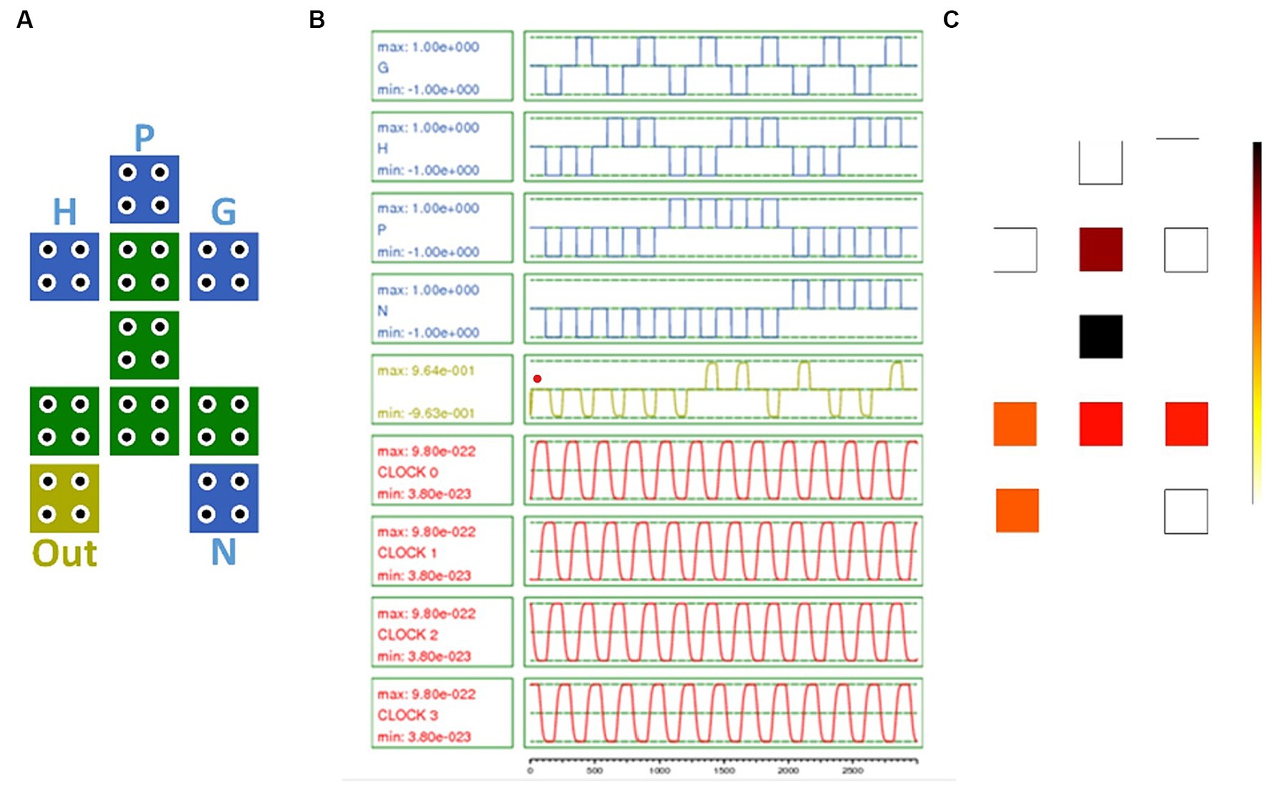
Figure 4. (A) Proposed gate simulation (B) Simulation results and (C) Energy dissipation map with.
The area of the proposed block is 0.011 μm2. The scheme is designed in a single layer and lacks cross-coupling methods. Using one clock phase reduces the delay in the proposed gate. As shown in Table 2, the proposed block enables the implementation of a wide range of basic functions. By simply changing the input values in the proposed block unit structure, various basic operations such as AND, OR, NOT, BUFFER, XOR, XNOR, Multiplexer (MUX), majority logic, and a three-input exclusive OR can be performed.
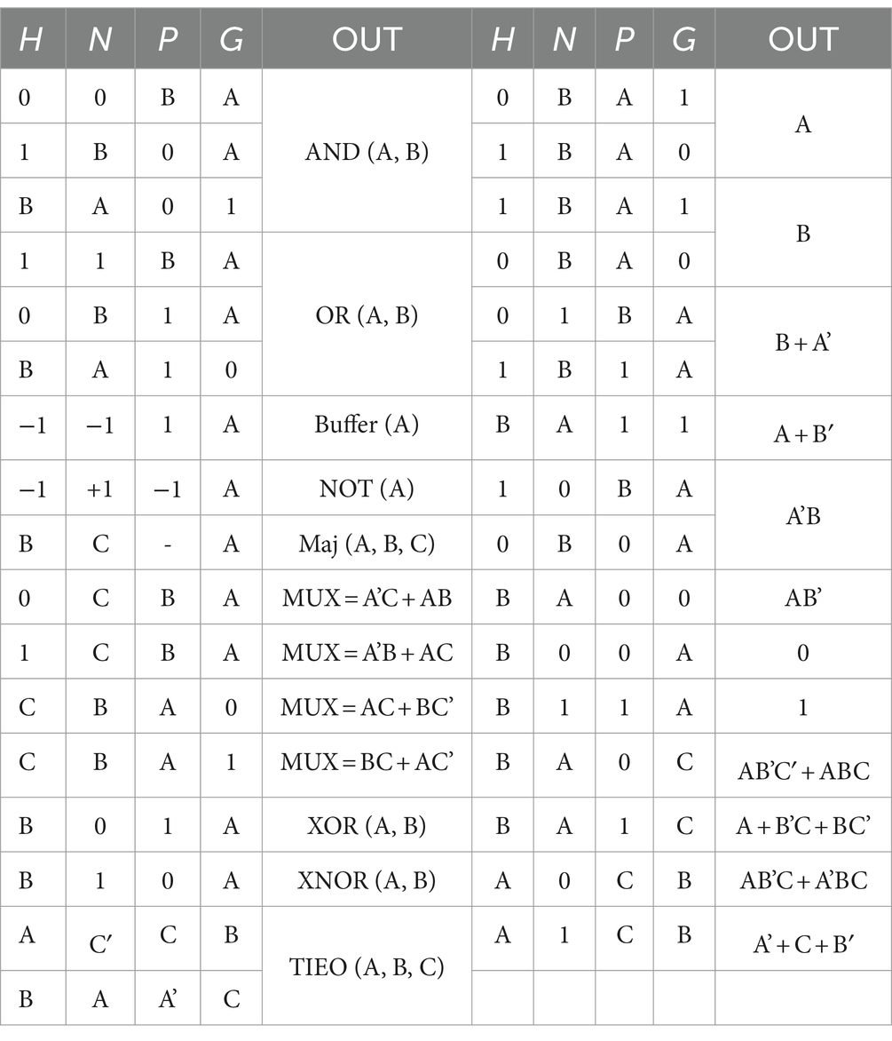
Table 2. Logic functions implemented by the proposed MGDI cell.
It should be noted that to simulate the proposed block and all the circuits designed using the proposed block, QCADesigner-E software in 18 nm technology using default simulation parameters according to Table 3 and using dual vector simulator engines and coherence vector has been done. Also, to determine the amount of energy consumed and draw its distribution map, the QCAPro simulator has been used. The energy utilization of the proposed block, under three different energy levels, is meticulously detailed and tabulated in Table 3.
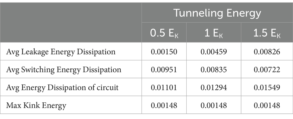
Table 3. Energy analysis of suggested IGDI-QCA cell.
Table 4 provides the consumed energy of the proposed block at three energy levels, calculated and presented according to the method proposed in Timler and Lent (2002). The static energy stemming from leakage power is significantly lower than the dynamic energy arising from switching, displaying a similar state to circuits of CMOS technology. The average energy dissipation of the circuit, represented by Ebath_total, is estimated as the sum (Ebath) for each clock pulse cycle by each cell in the design, aiming to illustrate the overall wasted energy. In the following, several complex circuits are designed and simulated using the proposed block IGDI-QCA.
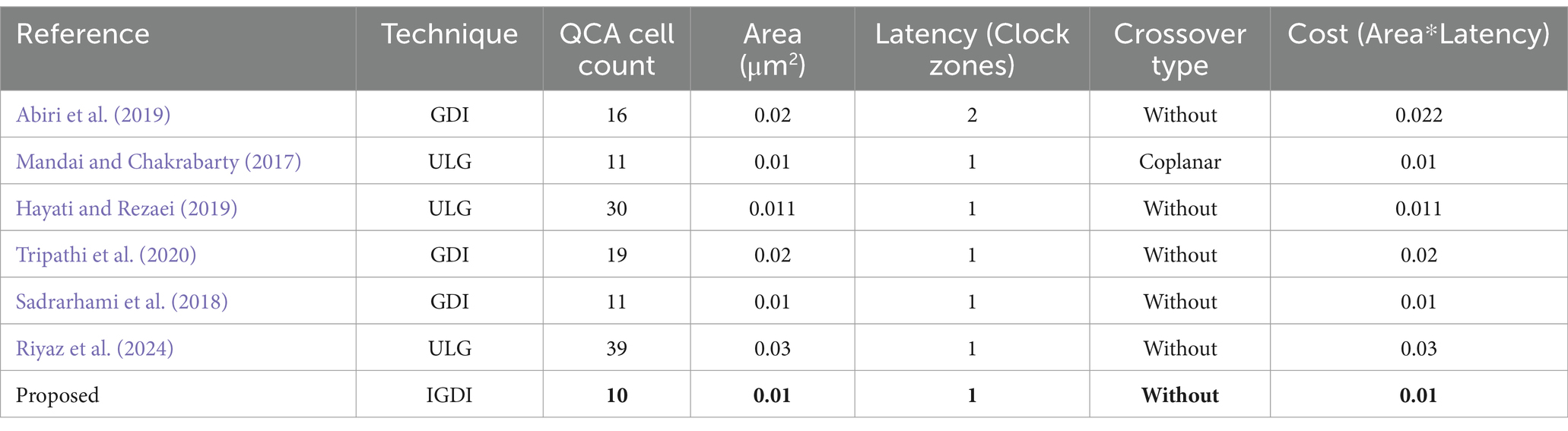
Table 4. Assessing the suggested IGDI cell in comparison to other existing works.
3 Designed combinational and sequential circuits using the proposed IGDI-QCA block
This part of the paper focuses on demonstrating the effectiveness of the proposed IGDI-QCA block by designing and simulating a range of commonly used logic and computational circuits. In addition to the mentioned basic gates, connecting multiple proposed blocks, more complex combinational and sequential circuits can be designed. An example of this application is the design of a single-bit comparator circuit using the IGDI-QCA block. The comparator is a crucial component in the decision-making processes of complex computing circuits. Its detailed structure, circuit design, simulation outcomes, and energy consumption metrics are comprehensively depicted in Figure 5. Optimizing the comparator circuit improves other circuits that use this gate.
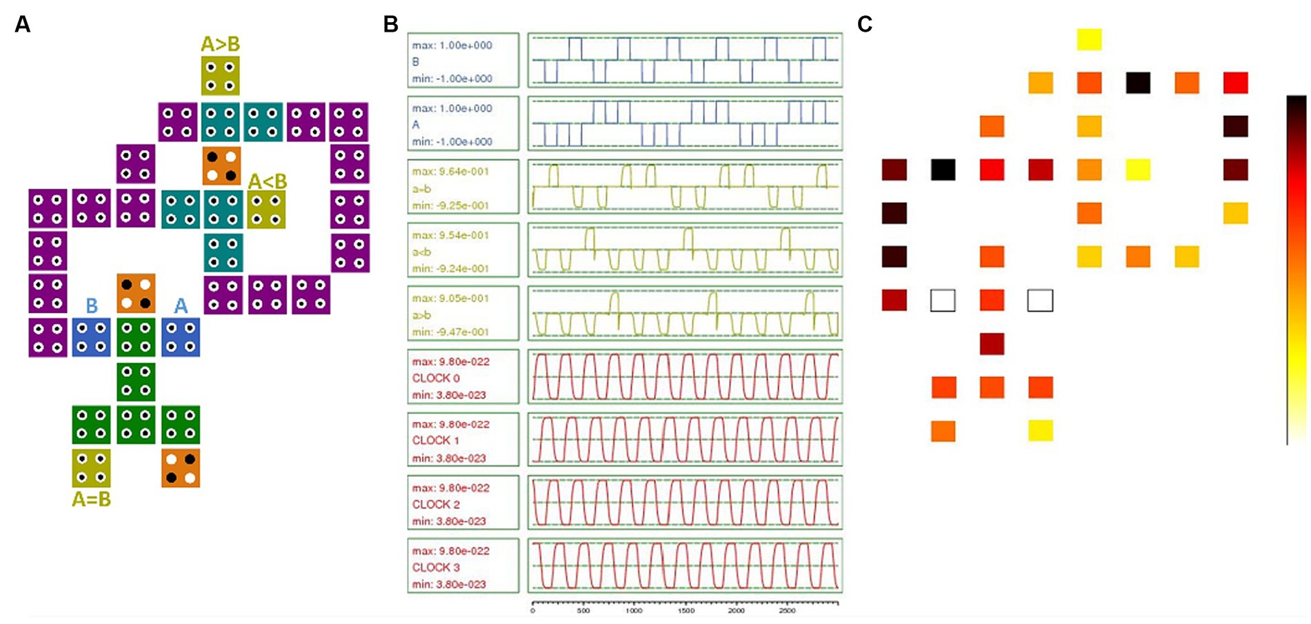
Figure 5. single-bit comparator using the proposed cell. (A) Proposed circuit simulation (B) Simulation results and (C) Energy dissipation map with 0.5 Ek.
Similarly, the application of the proposed IGDI-QCA block is further exemplified through the design of a four-bit parity generator circuit, as showcased in Figure 6. The four-bit parity generator is used in error detection in digital storage and communication systems. Producing a parity bit ensures the data integrity by checking whether the number of set bits is odd or even.
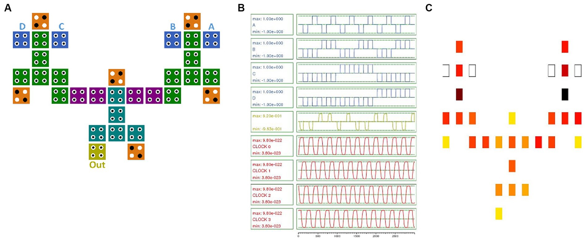
Figure 6. 4-bit parity generator using the IGDI-QCA cell. (A) Proposed circuit simulation (B) Simulation results and (C) Energy dissipation map with 0.5 Ek.
The importance of memory circuits in modern computing cannot be overstated, as they are crucial for data storage and retrieval, directly impacting the speed and efficiency of computational processes. QCA plays a pivotal role in the development of high-speed memory circuits. This article introduces a novel three-layer reversible memory structure in QCA, utilizing the advanced IGDI block. The memory design consists of 27 cells and operates across two clock phases, as illustrated in Figure 7.
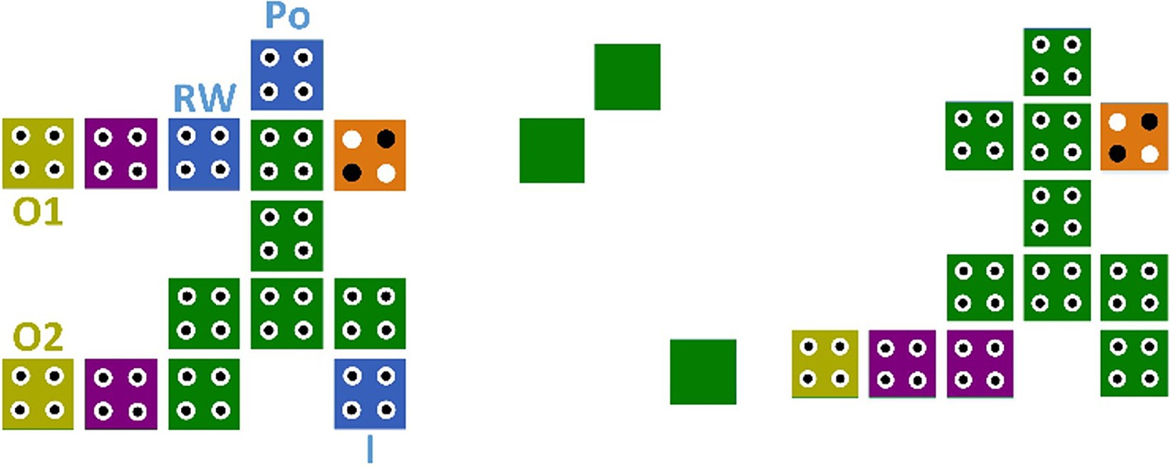
Figure 7. Proposed reversible memory layers.
The equations governing the three outputs of this proposed memory design are meticulously detailed in equation (3).
The subsequent section will delve into a detailed evaluation and comparison of these circuits, underscoring the benefits of the proposed block.
4 Comparison
In this section, the outcomes of the proposed design are juxtaposed with prior studies. The sequential and combinational circuits fashioned by the proposed block are scrutinized against analogous circuits from earlier research, focusing on metrics like area, delay, and quantum cost. The proposed circuit is simulated using QCADesigner-E version 2.0.3 in 18-nanometer technology. Both dual vector and coherence vector simulation engines are employed to ascertain cell polarization with default parameters, yielding congruent results and affirming the design’s accuracy. Comparison in Table 4 reveals the superiority of the proposed IGDI-QCA block in terms of cell count, area, and delay over prior works. When considering the cost function, defined as the product of area occupation and delay, only references (Mosleh, 2019; Perri et al., 2022) exhibit similar costs. Notably, reference (Mosleh, 2019) utilizes a coplanar type circuit, while reference (Perri et al., 2022) entails 11 cells. These insights are graphically depicted in Figure 8. Energy consumption is evaluated using QCAPro, indicating the proposed design’s lower energy consumption relative to other works. Furthermore, Figure 9 illustrates the assessment results for total and average dissipated energy (Table 5).
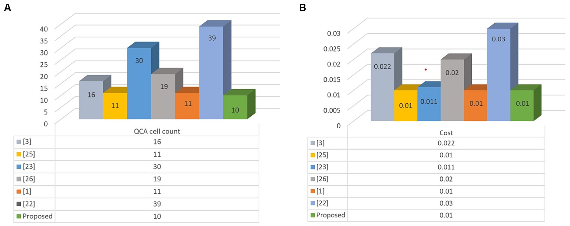
Figure 8. Comparison between the suggested block and existing works. (A) Number of cells (B) cost.
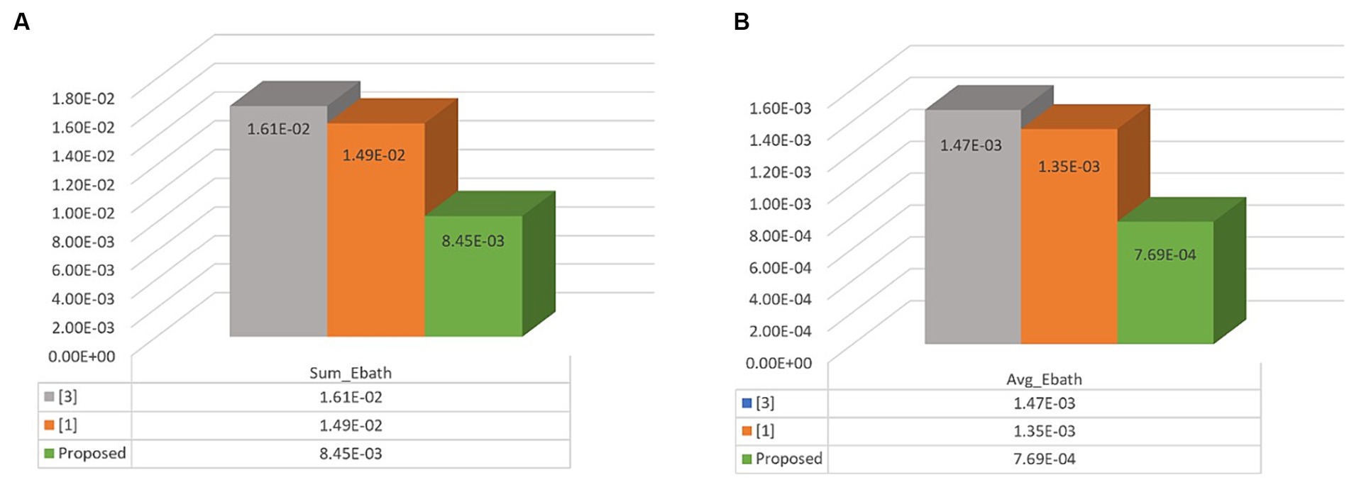
Figure 9. (A) Evaluation of the total energy consumed, (B) average energy consumed by the proposed.
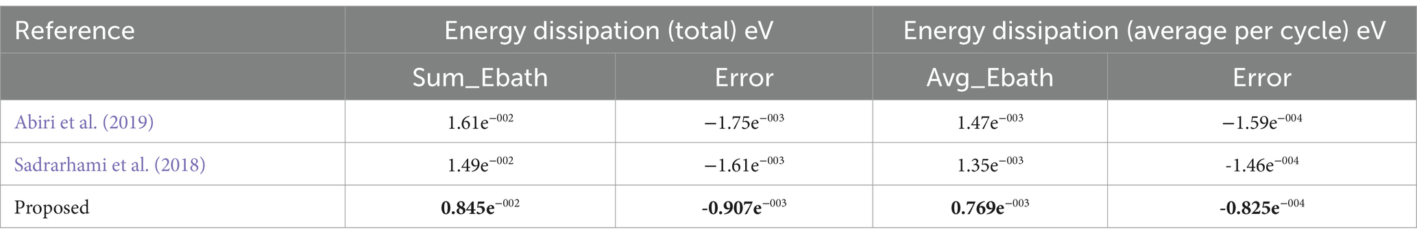
Table 5. Results of evaluation of energy lost in the proposed IGDI-QCA cell and previous works.
Table 6 in the paper offers a comparative analysis between various 2/1 Multiplexers from prior studies and the proposed design. The proposed MUX gate, in number of cells compared to reference (Ahmadpour et al., 2022), and area compared to works presented in references (Rashidi et al., 2016; Naji Asfestani and Rasouli Heikalabad, 2017; Sushma et al., 2021; Ahmadpour et al., 2022), and delay compared to Naji Asfestani and Rasouli Heikalabad (2017), Shiri et al. (2019), Sushma et al. (2021) and Sreevani et al. (2023) and cost compared to Naji Asfestani and Rasouli Heikalabad (2017), and Sushma et al. (2021), shows no improvement. So, the analysis of Table 7 shows that the proposed MUX has the lowest number of cells compared to other works and is in an optimal state in other parameters.
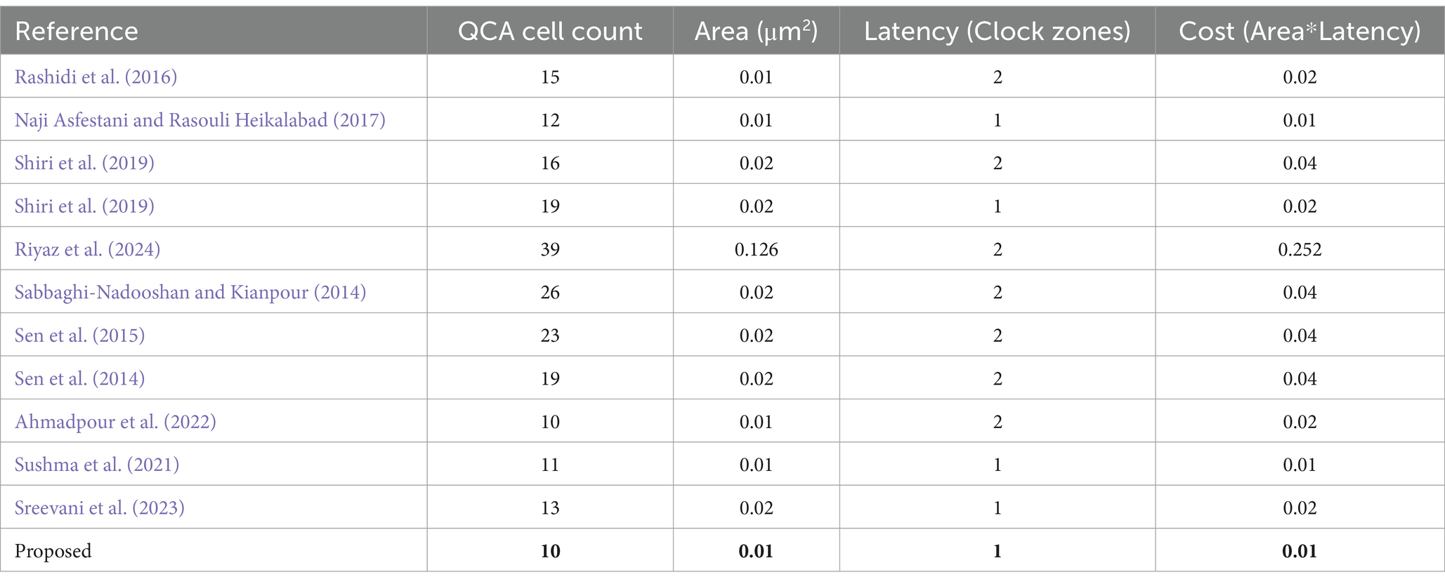
Table 6. Comparison results of MUX 2 * 1 in the proposed design with previous works.
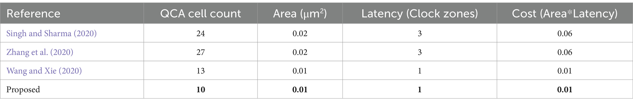
Table 7. Comparative results of XOR gate.
According to Table 7, although the proposed X-circuit is the same as the reference (Wang and Xie, 2020) in terms of area, delay, and cost, it is better than all previous works in terms of the number of blocks.
As can be seen in Table 8, the reference comparator circuit (Shiri et al., 2019) has better results in terms of area, delay, and cost compared to the proposed scheme, while the proposed circuit is better than all the previous works in terms of the number of cells.
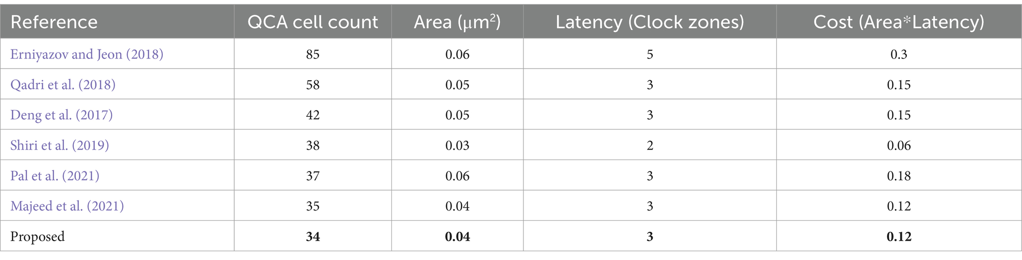
Table 8. Comparison result of single bit comparator.
Table 9 in the article presents a comparative analysis of various 4-bit parity generators from past studies alongside the proposed design. While the circuit mentioned in Gassoumi et al. (2019), Safoev et al. (2022) shows better results in terms of area, and reference (Safoev et al., 2022) outperforms the proposed design in terms of cost, the proposed IGDI-QCA-based design notably excels in other aspects. Specifically, it shows a significant 31% improvement in cell count efficiency compared to previous models.
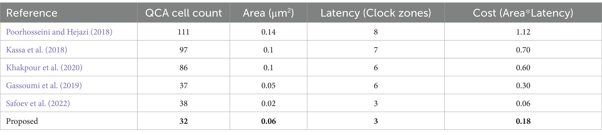
Table 9. 4-bit parity generator comparison results.
A comparative analysis of various memory designs is detailed in Table 10. The results show that the proposed design performs similarly to the circuit in reference (Macrae, 2022) in terms of area and cost, but it is superior in terms of the number of cells. Reference (Salimzadeh et al., 2020) is equivalent to the proposed work in terms of area and delay.
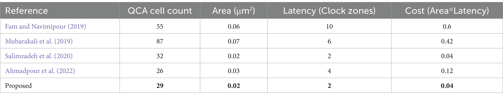
Table 10. RAM comparison results.
Furthermore, compared to the circuit mentioned in Sadeghi et al. (2020), the proposed memory design, leveraging the capabilities of the IGDI-QCA block, shows remarkable improvements. Specifically, it achieves a 34% reduction in area, 50% in delay, and 67% in overall cost. It’s noteworthy that the circuit from Sadeghi et al. (2020) utilizes a combination of four AND gates, and one each of OR, NOT, and MUX gates. This configuration contributes to an increased area and delay in their design. In contrast, the proposed circuit effectively addresses these issues by integrating the efficient IGDI-QCA block, resulting in a more compact, faster, and cost-effective memory circuit solution.
It’s important to note that the novelty of the presented manuscript lies in the improvement and modification of the conventional GDI structure from a 3-input to a 4-input configuration. As indicated in Table 2, this structure can perform 33 different functions compared to 6 functions achievable by the traditional GDI structure. Additionally, to evaluate the proposed block, several combinational and sequential circuits have been designed using it and compared with existing works, demonstrating the efficiency of the proposed block.
5 Conclusion
This paper introduced an innovative four-input GDI variant, termed Improved GDI (IGDI), achieved through an Improvement of the traditional GDI structure. Subsequently, this IGDI has been adapted and tested within QCA technology. The IGDI block, comprising a mere 10 cells, emerges as a versatile design unit capable of performing basic Medium-Scale Integration (MSI) combinational functions and being integral to sequential circuits.
A key feature of the IGDI block is the absence of cross-wiring, which significantly enhances the circuit’s operational efficiency. Its universal cell nature allows for implementing various logical gates by merely altering input values without necessitating any structural redesign. Consequently, by setting one of the inputs to either “0” or “1,” the block can effectively realize gates such as AND, OR, XOR, and MUX within the IGDI-QCA framework. This flexibility leads to notable improvements in aspects like energy efficiency, cell count reduction, and occupied area minimization. Furthermore, the IGDI block is adept at designing other basic combinational functions including NOT, BUFFER, XNOR, and Majority (Maj). The design and simulation outcomes for sequential functions, such as reversible memory, highlight the significant reduction in cell count achieved by the proposed cell compared to previous models. Additionally, the decrease in overall energy consumption (Sum_Ebath) and the cost function are key benefits of this innovative design, underscoring its potential for advancing circuit technology.
Data availability statement
The original contributions presented in the study are included in the article/supplementary material, further inquiries can be directed to the corresponding author.
Author contributions
HS: Conceptualization, Data curation, Formal analysis, Funding acquisition, Investigation, Methodology, Project administration, Resources, Software, Supervision, Validation, Visualization, Writing – original draft, Writing – review & editing. SZ: Conceptualization, Data curation, Formal analysis, Funding acquisition, Investigation, Methodology, Project administration, Resources, Software, Supervision, Validation, Visualization, Writing – original draft, Writing – review & editing. MD: Supervision, Writing – review & editing. BB: Supervision, Writing – review & editing.
Funding
The author(s) declare that no financial support was received for the research, authorship, and/or publication of this article.
Conflict of interest
The authors declare that the research was conducted in the absence of any commercial or financial relationships that could be construed as a potential conflict of interest.
Publisher’s note
All claims expressed in this article are solely those of the authors and do not necessarily represent those of their affiliated organizations, or those of the publisher, the editors and the reviewers. Any product that may be evaluated in this article, or claim that may be made by its manufacturer, is not guaranteed or endorsed by the publisher.
References
Abiri, E., Darabi, A., and Sadeghi, A. (2019). Gate-diffusion input (GDI) method for designing energy-efficient circuits in analogue voltage-mode fuzzy and QCA systems. Microelectron. J. 87, 81–100. doi: 10.1016/j.mejo.2019.04.001
Abiri, E., Salehi, M. R., and Darabi, A., “Design and evaluation of low power and high speed logic circuit based on the modified gate diffusion input (m-GDI) technique in 32nm CNTFET technology,”In 22nd Iranian Conference on Electrical Engineering. (2014). Tehran, Iran: IEEE. 67–72.
Abutaleb, M. M. (2018). Robust and efficient QCA cell-based nanostructures of elementary reversible logic gates. J. Supercomput. 74, 6258–6274. doi: 10.1007/s11227-018-2550-z
Ahmadpour, S. S., Mosleh, M., and Rasouli Heikalabad, S. (2022). Efficient designs of quantum-dot cellular automata multiplexer and RAM with physical proof along with power analysis. J. Supercomput. 78, 1672–1695. doi: 10.1007/s11227-021-03913-2
Ahmadpour, S. S., Navimipour, N. J., Mosleh, M., and Yalcin, S. (2023). Nano-design of ultra-efficient reversible block based on quantum-dot cellular automata. Front. Inf. Technol. Electron. Eng. 24, 447–456. doi: 10.1631/FITEE.2200095
Bhat, S. M., Ahmed, S., Bahar, A. N., Wahid, K. A., Otsuki, A., and Singh, P. (2023). Design of Cost-Efficient SRAM cell in quantum dot cellular automata technology. Electronics 12:367. doi: 10.3390/electronics12020367
Cardenas-Barrera, J. L., Plataniotis, K. N., and Venetsanopoulos, A. N. (2002). QCA implementation of a multichannel filter for image processing. Math. Probl. Eng. 8, 87–99. doi: 10.1080/10241230211381
Chen, H., Lv, H., Zhang, Z., Cheng, X., and Xie, G. (2019). Design and analysis of a novel low-power exclusive-OR gate based on quantum-dot cellular automata. J. Circuits Syst. Comput. 28, 1950141–1950117. doi: 10.1142/S021812661950141X
Deng, F., Xie, G., Zhang, Y., Peng, F., and Lv, H. (2017). A novel design and analysis of comparator with XNOR gate for QCA. Microprocess. Microsyst. 55, 131–135. doi: 10.1016/j.micpro.2017.10.009
Erniyazov, S., and Jeon, J.-C. (2018). Area efficient magnitude comparator based on QCA. Adv. Sci. Technol. Lett. 150, 75–79,
Fam, S. R., and Navimipour, N. J. (2019). Design of a loop-based random access memory based on the nanoscale quantum dot cellular automata. Photonic Netw. Commun. 37, 120–130. doi: 10.1007/s11107-018-0801-9
Gassoumi, I., Touil, L., Ouni, B., and Mtibaa, A. (2019). An ultra-low power parity generator circuit based on QCA technology. J. Electr. Comput. Eng. 2019, 1–8. doi: 10.1155/2019/1675169
Ghorbani, A., Dolatshahi, M., Zanjani, S. M., and Barekatain, B. (2022). A new low-power dynamic-GDI full adder in CNFET technology. Integration 83, 46–59. doi: 10.1016/j.vlsi.2021.12.001
Gupta, S., and Wairya, S. (2016). A GDI approach to various combinational logic circuits in CMOS Nano Technology. Int. J. of Adv. Trend Comp. Sci. Eng. 2016:38. doi: 10.18535/ijecs/v5i4.38
Hayati, M., and Rezaei, A. (2019). Design of a new Optimized Universal Logic Gate for quantum-dot cellular automata. IETE J. Res. 68, 1141–1147. doi: 10.1080/03772063.2019.1643262
Huang, J., and Ottavi, M. (2005). Tile-based QCA design using majority-like logic primitives tile-based QCA design using majority-like logic primitives. ACM J. Emerg. Technol. Comput. Syst. 1, 163–185. doi: 10.1145/1116696.1116697
Kassa, S. R., Nagaria, R. K., and Karthik, R. (2018). Energy efficient neoteric design of a 3-input majority gate with its implementation and physical proof in quantum dot cellular automata. Nano Commun. Netw. 15, 28–40. doi: 10.1016/j.nancom.2018.02.001
Khakpour, M., Gholami, M., and Naghizadeh, S. (2020). Parity generator and digital code converter in QCA nanotechnology. Int. Nano Lett. 10, 49–59. doi: 10.1007/s40089-019-00292-8
Khan, A., Parameshwara, M. C., and Arya, R. (2023). Defects of quantum dot cellular automata computing devices: an extensive review, evaluation, and future directions. Microprocess. Microsyst. 101:104912. doi: 10.1016/j.micpro.2023.104912
Liu, W., Srivastava, S., O’Neill, M., and Swartzlander, E. E., (2014), “Security issues in QCA circuit design - power analysis attacks,”In: Anderson, N., and Bhanja, S. (eds) Field-Coupled Nanocomputing, Springer, Berlin, Heidelberg.
Macrae, R. M. (2022). Mixed-valence realizations of quantum dot cellular automata. J. Phys. Chem. Solids 177:111303. doi: 10.1016/j.jpcs.2023.111303
Majeed, A. H., Zainal, M. S., Alkaldy, E., and Nor, D. M. (2021). Single-bit comparator in quantum-dot cellular automata (QCA) technology using novel QCA-XNOR gates. J. Electron. Sci. Technol. 19, 100078–100273. doi: 10.1016/j.jnlest.2020.100078
Mandai, N. K., and Chakrabarty, R., (2017), “Complementary dual-output universal gate in quantum dot cellular automata,”In 8th Annual Industrial Automation and Electromechanical Engineering. Bangkok, Thailand: IEEE. 321–323.
Mohammadi, H., and Navi, K. (2018). Energy-efficient single-layer QCA logical circuits based on a novel XOR gate. J. Circuits Syst. Comput. 27:1850216. doi: 10.1142/S021812661850216X
Mosleh, M. (2019). A novel full adder/subtractor in quantum-dot cellular automata. Int. J. Theor. Phys. 58, 221–246. doi: 10.1007/s10773-018-3925-x
Mubarakali, A., Ramakrishnan, J., Mavaluru, D., Elsir, A., Elsier, O., and Wakil, K. (2019). A new efficient design for random access memory based on quantum dot cellular automata nanotechnology. Nano Commun. Netw. 21:100252. doi: 10.1016/j.nancom.2019.100252
Naji Asfestani, M., and Rasouli Heikalabad, S. (2017). A unique structure for the multiplexer in quantum-dot cellular automata to create a revolution in design of nanostructures. Phys. B Condens. Matter 512, 91–99. doi: 10.1016/j.physb.2017.02.028
Naz, S. F., Riyaz, S., and Sharma, V. K. (2021). A review of QCA nanotechnology as an alternate to CMOS. Curr. Nanosci. 18, 18–30. doi: 10.2174/1573413717666210301111822
Pal, J., Noorallahzadeh, M., Sharma, J. S., Bhowmik, D., Saha, A. K., and Sen, B. (2021). Regular clocking scheme based design of cost-efficient comparator in QCA. Indones. J. Electr. Eng. Comput. Sci. 21, 44–55. doi: 10.11591/ijeecs.v21.i1.pp44-55
Perri, S., Spagnolo, F., Frustaci, F., and Corsonello, P. (2022). Multibit Full Comparator Logic in Quantum-Dot Cellular Automata. IEEE Trans Circuits Syst II Express Briefs 69, 4508–4512. doi: 10.1109/TCSII.2022.3193561
Poorhosseini, M., and Hejazi, A. R. (2018). A fault-tolerant and efficient XOR structure for modular design of complex QCA circuits. J. Circuits Syst. Comput. 27:1850115. doi: 10.1142/S0218126618501153
Qadri, S. U. R., Bangi, Z. A., Banday, M. T., and Bhat, G. M., (2018), “A novel cryptographic design in quantum dot cellular automata,” 4th International Conference on Computing Communication and Automation (ICCCA). Greater Noida, India: IEEE. 1–10.
Rashidi, H., Rezai, A., and Soltany, S. (2016). High-performance multiplexer architecture for quantum-dot cellular automata. J. Comput. Electron. 15, 968–981. doi: 10.1007/s10825-016-0832-3
Riyaz, S., Sharma, V. K., and Kaushik, N. (2024). Fault-tolerant universal reversible gate design in QCA nanotechnology. e-Prime 7:100435. doi: 10.1016/j.prime.2024.100435
Sabbaghi-Nadooshan, R., and Kianpour, M. (2014). A novel QCA implementation of MUX-based universal shift register. J. Comput. Electron. 13, 198–210. doi: 10.1007/s10825-013-0500-9
Sadeghi, M., Navi, K., and Dolatshahi, M. (2020). Novel efficient full adder and full subtractor designs in quantum cellular automata. J. Supercomput. 76, 2191–2205. doi: 10.1007/s11227-019-03073-4
Sadrarhami, H., Zanjani, S. M., Dolatshahi, M., and Barekatain, B. (2018). Designing a new gate-diffusion input in quantum-dot cellular automata technology. J. Intell. Proced. Electr. Technol. 16, 63–78. doi: 10.20944/preprints202311.1295.v1
Safaiezadeh, B., Kettunen, L., and Haghparast, M. (2023). Novel high-performance QCA Fredkin gate and designing scalable QCA binary to gray and vice versa. J. Supercomput. 79, 7037–7060. doi: 10.1007/s11227-022-04939-w
Safoev, N., Ahmed, S., Tashev, K., and Naz, S. F. (2022). Design of fault tolerant bifunctional parity generator and scalable code converters based on QCA technology. Int. J. Inf. Technol. 14, 991–998. doi: 10.1007/s41870-021-00730-x
Salimzadeh, F., Heikalabad, S. R., and Gharehchopogh, F. S. (2020). Design of a reversible structure for memory in quantum-dot cellular automata. Int. J. Circuit Theory Appl. 48, 2257–2265. doi: 10.1002/cta.2807
Sen, B., Dutta, M., Goswami, M., and Sikdar, B. K. (2014). Modular design of testable reversible ALU by QCA multiplexer with increase in programmability. Microelectron. J. 45, 1522–1532. doi: 10.1016/j.mejo.2014.08.012
Sen, B., Goswami, M., Mazumdar, S., and Sikdar, B. K. (2015). Towards modular design of reliable quantum-dot cellular automata logic circuit using multiplexers. Comput. Electr. Eng. 45, 42–54. doi: 10.1016/j.compeleceng.2015.05.001
Shiri, A., Rezai, A., and Mahmoodian, H. (2019). Design of efficient coplanar comprator circuit in QCA technology. Facta Univ., Electron. Energ. 32, 119–128. doi: 10.2298/FUEE1901119S
Singh, R., and Sharma, D. K. (2020). “Area efficient multilayer designs of XOR gate using quantum dot cellular automata” in Micro-electronics and telecommunication engineering. eds. D. K. Sharma, V. E. Balas, L. H. Son, R. Sharma, and K. Cengiz (Singapore: Springer), 693–705.
Sreevani, M., Vijay, V., Chaitanya, K., Radhika, C., Manjula, N., Radha Krishna Koushik, D., et al. (2023). State-of-art design: data selectors using quantum-dot cellular automata. Int. J. Syst. Assur. Eng. Manag. 15, 1285–1293. doi: 10.1007/s13198-023-02215-5
Sushma, S., Swathi, S., and Bindusree, V., (2021), “QCA based universal shift register using 2 to 1 mux and D flip-flop,”In International Conference on Advances in Computing, Communication, and Control (ICAC3), IEEE: Mumbai, India. 1–6.
Timler, J., and Lent, C. S. (2002). Power gain and dissipation in quantum-dot cellular automata. J. Appl. Phys. 91, 823–831. doi: 10.1063/1.1421217
Tougaw, P. D., et al. (2021). Logical devices implemented using quantum cellular automata. Appl. Sci. 75, 1818–1825,
Tripathi, D., Sana, S., and Wairya, S., (2020). Cell Optimization and Realization of MGDI and QCA based combinational logic circuits for nanotechnology applications, In 17th India council international conference (INDICON). New Delhi, India: IEEE. 1–8.
Wang, L., and Xie, G. (2018). Novel designs of full adder in quantum-dot cellular automata technology. J. Supercomput. 74, 4798–4816. doi: 10.1007/s11227-018-2481-8
Wang, L., and Xie, G. (2020). A novel XOR/XNOR structure for modular design of QCA circuits. IEEE Trans Circuits Syst II Express Briefs 67, 3327–3331. doi: 10.1109/TCSII.2020.2989496
Keywords: improved gate diffusion input, quantum-dot cellular automata, polarization, QCADesigner, low-power
Citation: Sadrarhami H, Zanjani SM, Dolatshahi M and Barekatain B (2024) Design and simulation of a new QCA-based low-power universal gate. Front. Comput. Sci. 6:1373906. doi: 10.3389/fcomp.2024.1373906
Edited by:
Niusha Shafiabady, Charles Darwin University, AustraliaReviewed by:
Yubing Shi, Shaanxi University of Chinese Medicine, ChinaAsif Karim, Charles Darwin University, Australia
Copyright © 2024 Sadrarhami, Zanjani, Dolatshahi and Barekatain. This is an open-access article distributed under the terms of the Creative Commons Attribution License (CC BY). The use, distribution or reproduction in other forums is permitted, provided the original author(s) and the copyright owner(s) are credited and that the original publication in this journal is cited, in accordance with accepted academic practice. No use, distribution or reproduction is permitted which does not comply with these terms.
*Correspondence: S. Mohammadali Zanjani, sma_zanjani@pel.iaun.ac.ir