
Managing contamination delay to improve Timing Speculation architectures
- Published
- Accepted
- Received
- Academic Editor
- Soha Hassoun
- Subject Areas
- Algorithms and Analysis of Algorithms, Computer Architecture, Embedded Computing, Emerging Technologies
- Keywords
- Timing speculation, Timing errors, PVT variation, Overclocking, Delay insertion, Timing constraints, Reliable and aggressive systems, Contamination delay
- Copyright
- © 2016 Avirneni et al.
- Licence
- This is an open access article distributed under the terms of the Creative Commons Attribution License, which permits unrestricted use, distribution, reproduction and adaptation in any medium and for any purpose provided that it is properly attributed. For attribution, the original author(s), title, publication source (PeerJ Computer Science) and either DOI or URL of the article must be cited.
- Cite this article
- 2016. Managing contamination delay to improve Timing Speculation architectures. PeerJ Computer Science 2:e79 https://doi.org/10.7717/peerj-cs.79
Abstract
Timing Speculation (TS) is a widely known method for realizing better-than-worst-case systems. Aggressive clocking, realizable by TS, enable systems to operate beyond specified safe frequency limits to effectively exploit the data dependent circuit delay. However, the range of aggressive clocking for performance enhancement under TS is restricted by short paths. In this paper, we show that increasing the lengths of short paths of the circuit increases the effectiveness of TS, leading to performance improvement. Also, we propose an algorithm to efficiently add delay buffers to selected short paths while keeping down the area penalty. We present our algorithm results for ISCAS-85 suite and show that it is possible to increase the circuit contamination delay by up to 30% without affecting the propagation delay. We also explore the possibility of increasing short path delays further by relaxing the constraint on propagation delay and analyze the performance impact.
Introduction
Systems have traditionally been designed to function reliably for the worst case timing delays under adverse operating conditions. Such worst case scenarios occur rarely, allowing possible performance improvement by making common cases faster. Alternative to conventional methods, the concept of latching data speculatively is called Timing Speculation (TS) (Austin, 1999; Bezdek, 2006; Ernst et al., 2003; Greskamp et al., 2009; Greskamp & Torrellas, 2007; Avirneni & Somani, 2012; Subramanian et al., 2007). Dual latch based TS is a widely accepted methodology for designing better-than-worst-case digital circuits. Timing speculation based aggressive systems are designed on the philosophy that it is profitable to operate beyond worst-case limits to achieve best performance by not avoiding, but detecting and correcting a modest number of timing errors. Aggressive design methodology exploit the fact that timing critical paths are rarely exercised in a design and typical execution happens much faster. Recent works have also shown that the performance loss due to over provisioning based on worst-case design margins is upward of 20% in terms of operating frequency and upward of 50% in terms of power efficiency (Gupta et al., 2009). Timing speculation combined with timing error tolerance is a powerful technique to (1) achieve energy efficiency by under-volting, as in Razor (Ernst et al., 2003), or (2) performance enhancement by overclocking, as in SPRIT3E (Bezdek, 2006).
Dual latch based TS require additional clock resources for the replicated latches (or flip-flops), which are triggered by a phase shifted clock of the original register. Despite the area and routing overheads, the benefits achieved by dual latched TS remain immense (Ernst et al., 2003; Avirneni & Somani, 2012; Subramanian et al., 2007; Das et al., 2006; Ramesh, Subramanian & Somani, 2010; Avirneni & Somani, 2013; Avirneni, Ramesh & Somani, 2016). However, in Subramanian et al. (2007) it has been pointed out that the performance benefits realized through TS is limited by the short paths of the circuit. It is due to the tight timing constraints that need to met for error recovery. This problem is compounded when circuits have a significantly lower contamination delay. The contamination delay is defined as the smallest time it takes a circuit to change any of its outputs, when there is a change in the input. It has been shown that for a carry-look ahead (CLA) adder significant performance enhancement is achieved when its contamination delay is increased by adding buffers (Subramanian et al., 2007). Increasing the delay of all shorter paths in the circuit above a desired lower bound, while not affecting the critical path is one of the steps performed during synthesis of sequential circuits to fix hold time violations. However, increasing the contamination delay of a logic circuit significantly, sometimes as high as half the propagation delay, without affecting its propagation delay is not a trivial issue (Shenoy, Brayton & Sangiovanni-Vincentelli, 1993). At the first glance, it might appear that adding delay by inserting buffers to the shortest paths will solve the problem. However, delay of a circuit is strongly input value dependent, and the structure of the circuit plays a role in deciding the value of an output in a particular cycle. Current synthesis tools support increasing the delay of short paths through their hold violation fixing option.
Our major goal in this paper is to extend the hold time of the replicated register present in dual latch TS framework. Traditional delay optimization approaches consider only part of the problem, viz., to ensure that the delay of each path is less than a fixed upper bound. The closest work we are aware of is presented in Chen & Muroga (1991), which uses timing optimization algorithm, Sylon-Dream Level-Reduction (SDLR), to speed up multi-level networks. The non-critical paths are processed by an area reduction procedure to reduce network area without increasing the maximum depth. SDLR uses the concept of permissible functions in both level and area reduction processes.
Contribution
The existing techniques only attempt to confine the critical path delay under design specified threshold. For TS architectures, the delay optimization algorithms must also make sure that the short paths satisfy imposed threshold requirements to increase the extent of performance enhancement. This is, in addition to the existing short path timing constrains free of any hold time violations. This aspect of our work makes it different from any of the existing works. As far as we know, this is the first work aimed at increasing the contamination delay of digital circuits up to a given threshold, beyond satisfying hold time violations. In this paper, we make three significant contributions.
First, we present a detailed timing analysis of a dual latch TS framework and quantify the margin for performance enhancement while operating beyond worst case.
Second, we study the impact of short paths on performance of Alpha processor core, where we present a sensitivity analysis of the achievable performance gain for different settings of contamination delay. In that process, we establish a case for increasing contamination delay of circuits in aggressive systems to improve the extent of performance enhancement.
Third, we present an algorithm to add delay buffers for dual latch TS framework. Specifically, we develop a weighted graph model to represent a multi-level digital circuit. We showcase a new min-arc algorithm that operates on the graph network to increase short path delays by adding buffers to selective interconnections. We consider each interconnection, whether it lies on the critical path, short path, or not. Depending upon how far each section of the circuit is from the maximum and minimum delayed paths, fixed delay buffers are added.
The presented algorithm is evaluated using ISCAS’85 benchmark suite. In our simulations, we investigate the increase in short path delays with and without relaxing critical path delays of these circuits. Also, we analyze the area and power overhead due to the addition of delay buffers at extreme corners. Using our new algorithm, we were able to increase the contamination delay to 30% of the circuit critical path length and also without affecting its propagation delay. We were further able to increase the contamination delay by relaxing the propagation delay constraint for a larger gain in performance.
The remainder of this paper is organized as follows. ‘Timing Speculation Framework’ provides an overview of dual-latch TS framework. ‘Performance Impact of Short Paths’ investigates the timing constraints of TS framework and ‘Increasing Short Path Delays’ presents the challenges of increasing short path delays. In ‘Performance & Contamination Delay: A Study on Alpha Processor’, we present our case study on Alpha processor. Following this, we present the network model and the algorithm for manipulating short paths of the circuit in ‘Min-arc Algorithm for Increasing Short Path Delays.’ Results of our experiments are presented in ‘Evaluation of Min-arc Method.’ We present a brief literature review in ‘Related Literature’ and summarize our concluding remarks and future directions in ‘Conclusions.’
Timing Speculation Framework
In a pipelined architecture, a timing error occurs if changes in the input propagate through the combinational logic before the computed results for the previous input are latched. The timing errors also occur due to the mismatch between the circuit propagation delay and the clock cycle time. Therefore, in a pipelined processor, the clock frequency is determined based on the circuit critical path across all stages under the most adverse operating conditions. Traditional design methodologies for the worst-case operating conditions are too conservative, as the critical timing delays rarely occur in tandem during typical circuit operation. Such infrequent occurrence of critical timing delays opens up a new domain of study that allows improvement of processor performance to a greater extent. During execution, delay incurred by the digital circuit is much less than the worst-case delay. This can be exploited by making common cases faster. Timing speculation is a technique wherein data generated at aggressive speeds are latched and sent forward speculatively assuming error free operation. Error detection is deployed to detect a timing violation. When an error is detected, the forwarded data is voided and the computation is performed again as part of the recovery action. A framework to achieve this is described below.
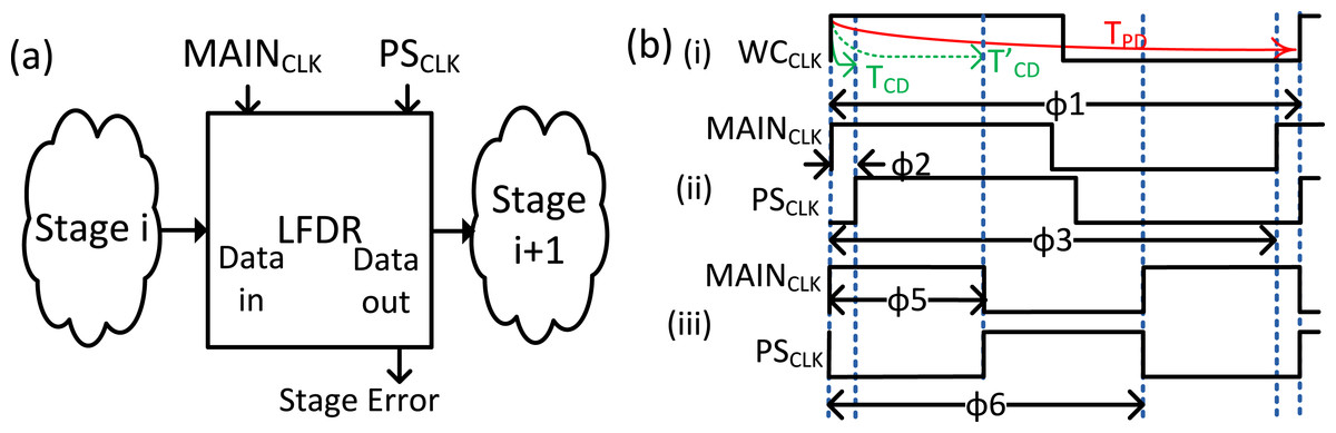
Figure 1: (A) Typical pipeline stage in a reliably overclocked processor (B) Illustration of aggressive MAIN and PS clocks for circuits with different contamination delays.
Dual latched system
We first present a brief description of a dual latched timing speculation framework from Bezdek (2006). We refer to this framework as Local Fault Detection and Recovery (LFDR). Figure 1A presents the LFDR circuit in between two pipeline stages. To reliably overclock a system dynamically using LFDR framework, we need two clocks: MAINCLK and PSCLK. The two clocks relationship is governed by timing requirements that are to be met at all times. LFDR consists of two registers: a main register clocked ambitiously by MAINCLK, which is running at a frequency higher than that is required for error-free operation; and a backup register clocked by PSCLK, which has same frequency as MAINCLK but is phase shifted. This amount of phase shift is such that backup register always sample the data by meeting the worst-case propagation delay time of the combinational circuit. The timing diagram shown in Fig. 1B illustrate the phase relationship between these clocks. Here, case (i) presents the worst case clock, WCCLK, with time period Φ1, which covers the maximum propagation delay. Case (ii) shows TS scenario, where the clock time period is reduced to Φ3. However, PSCLK is delayed by Φ2 in such a way that the next rising edge of PSCLK coincide with next rising edge of WCCLK. Thus a computation started at the rising edge of MAINCLK will successfully complete by the next rising edge of PSCLK. The key point to note here is that the amount of phase shift, Φ2, for the PSCLK is limited by the contamination delay, TCD, of the circuit.
Figure 2 shows timing waveforms that depict timing speculation using LFDR. In the figure, inst0 moves forward without any timing errors using speculation. However, inst1 encounters a timing error in Stagei, indicated by corrupted data “terr.” This error is detected by the error detection mechanism, and the stage error signal is asserted. This stage error signal triggers a local and global recovery. Timing error recovery flushes the data sent forward speculatively, indicated in the figure as “xxx,” and voids the computation performed by Stagei + 1. Once the timing error is fixed, the pipeline execution continues normally. It is clear from the waveform that the time gained by TS is Φ4, which is equal to Φ2.
A balance must be maintained between the number of cycles lost to error recovery and the gains of overclocking. One important factor that needs to be addressed while phase shifting the PSCLK is to limit the amount of phase shift within the fastest delay path of the circuit.
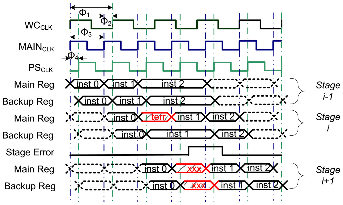
Figure 2: Timing diagram showing pipeline stage level timing speculation.
Performance Impact of Short Paths
The cardinal factor that limits data-dependent allowable frequency scaling for LFDR frameworks is the contamination delay of the circuit. The phase shift of the delayed clock is restricted by the contamination delay to prevent incorrect result from being latched in the backup register. Reliable execution can be guaranteed only if the contents of the redundant register are considered “golden.” To overcome this limitation, it is important to increase the contamination delay of the circuit. Case (iii) in Fig. 1B presents a TS scenario where the clock time period is reduce Φ6 and PSCLK is delayed by Φ5. As phase shift Φ5 is greater than Φ2, the range of achievable overclocking is higher in case (iii) than case (ii). From this example, we can conclude that having contamination delay increases the range of aggressive clocking under TS.
Let us denote the worst-case propagation delay and minimum contamination delay of the circuit as TPD and TCD, respectively. Let TWCCLK, TMAINCLK and TPSCLK represent the clock periods of WCCLK, MAINCLK and PSCLK, respectively. Let TPS represent the amount of phase-shift between MAINCLK and PSCLK. Also we will denote TOV as the overclocked time period.
At all times, the following equations hold. (1) (2) (3)
Let FMIN be the setting when there is no overclocking i.e., TOV = TPD. In this case, TPS = 0. The maximum possible frequency, FMAX permitted by reliable overclocking is governed by TCD. This is because short paths in the circuit, whose delay determine TCD, can corrupt the data latched in the backup register. If the phase shift TPS is greater than TCD, then the data launched can corrupt the backup register at PSCLK edge. If such a corruption happens, then the backup register may latch incorrect result and cannot be considered “golden.” Hence, it is not possible to overclock further than FMAX. The following equations should hold at all times to guarantee reliable overclocking.
(4) (5)
For any intermediate overclocked frequency, FINT, between FMIN and FMAX, TPS ≤ TCD. During operation, FINT is determined dynamically based on the number of timing errors being observed during a specific duration of time. The dependence of phase shift on contamination delay leads directly to the limitation of the aggressive frequency scaling. A simplistic notion of the maximum speed-up that is achievable through reliable overclocking is given by Eq. (6). (6)
Increasing Short Path Delays
It is clear from Eq. (6) that the maximum speedup is achieved when the difference between the contamination delay and propagation delay is minimal. However, it must be noted that increasing TCD also affects the margin for overclocking. To overcome this challenge, we develop a technique for increasing the contamination delay to a moderate extent without affecting the propagation delay of the circuit. As outputs of the combinational logic depends on several inputs, and more than one path to each output exists, with both shorter and longer paths overlapping, adding buffer delays to shorter paths may increase the overall propagation delay of the circuit. The main challenge is to carefully study the delay patterns, and distribute the delay buffers across the interconnections. More importantly, the overall propagation delay must remain unchanged. However, it may not be possible to constrain propagation delay of the critical paths due to logic/interconnection sharing in the network.
Most practical circuits have significantly lower contamination delay. For instance, we verified that an 8-bit CLA adder circuit, implemented in 0.18 µm Cadence Generic Standard Cell Library (GSCLib), has a propagation delay of 1.06 ns, but an insignificant contamination delay of 0.06 ns, thus allowing almost no performance improvement through reliable overclocking. It should be noted that the outputs of CLA adder depends on more than one inputs, thus a trivial addition of delay buffers to short paths results in increased propagation delay of the circuit. However, by re-distributing the delay buffers all to one side (either input or output), it is possible to increase contamination delay, without affecting the propagation delay, by up to 0.37 ns.
Increasing circuit path delay above a desired level without affecting critical path is not uncommon in sequential circuit synthesis. In fact, it is performed as a mandatory step during synthesis operation. In a sequential circuit, for an input signal to be latched correctly by an active clock edge, it must become stable before a specified time. This duration before the clock edge is called the set up time of the latch. The input signal must remain stable for a specified time interval after the active clock edge in order to get sampled correctly. This interval is called the hold time of the latch. Any signal change in the input before the next set-up time or after the current hold time does not affect the output until the next active clock edge. Clock skew, which is the difference in arrival times at the source and destination flip-flops, also exacerbates hold time requirements in sequential circuits. Hold time violations occur when the previous data is not held long enough. Hence, adding buffers to short paths that violate hold time criteria is a step that is carried out without too much of a concern regarding area and power overheads.
Increasing the contamination delay of a logic circuit significantly without affecting its propagation delay is not straightforward (Shenoy, Brayton & Sangiovanni-Vincentelli, 1993). At first glance, it might appear that adding delay by inserting buffers to the shortest paths will solve the problem. However, delay of a circuit is strongly input dependent, and several inputs play a role in deciding the value of an output in a particular cycle. Current synthesis tools support increasing the delay of short paths through their hold violation fixing option; in a broader sense, what we essentially want to do is to extend the hold time of the backup register.
Though it is possible to phase shift to a maximal extent, reducing the clock period by that amount may result in higher number of errors. Having a control over the increase in contamination delay gives us an advantage to tune the circuit’s frequency to the optimal value depending on the application and the frequency of occurrence of certain input combinations. Also, introducing delay to increase contamination delay increases the area of the circuit. Therefore, while judiciously increasing contamination delay we must also ensure that the increase in area is not exorbitant.
Performance & Contamination Delay: A Study on Alpha Processor
To demonstrate the effect of increasing short paths on performance, we conducted a simple study on Alpha processor model for different contamination delay settings. We ran selected set of SPEC 2000 benchmark workloads on SimpleScalar—a cycle accurate simulator (Burger & Austin, 1997). In order to embed timing aspects in SimpleScalar, we examined a hardware model of Alpha processor datapath and obtained the number of timing errors occurring at different clock period, for each workload. For this purpose we synthesized Illinois Verilog Model (IVM) for Alpha 21264 configuration using 45 nm OSU standard cell library (Stine et al., 2007). Although we are aware of the fact that the pipeline in IVM is simplistic, it does not have any impact on our results as we are performing a comparative study of different settings for the same circuit. In this experiment, we are exploring the impact of contamination delay on timing speculation framework at circuit level. Therefore, we believe our analysis and insights are applicable to other architectures as well.
We adopt the configuration close to hardware model for SimpleScalar simulations as well. The details of the settings are presented in Table 1 and more details about our hardware model can be found in Ramesh, Subramanian & Somani (2010). It is important to note that, for our hardware model, the timing critical path is in the Issue stage of the processor pipeline. Therefore, applications which are core bound will be effected more than the applications that are memory bound. In this study, we have presented the benchmarks which has higher error rate than the rest of the suite for all 32 equal intervals of the operating frequency. Therefore, performance results from this study present the lower bounds of speed-up that can be observed for SPEC benchmarks. Performance results for other benchmarks are bound to be higher than speed-up observed in our study.
| Parameter | Value |
|---|---|
| Fetch/Decode/Issue/Commit width | 4 inst/cycle |
| Functional units | 4 INT ALUs, 1 INT MUL/DIV, 4 FP ALUs, 1 FP MUL/DIV |
| L1 D-cache | 128K |
| L1 I-cache | 512K |
| L2 Unified | 1024K |
| Technology node | 45 nm |
| Base frequency | 2.5 GHz |
| No. of freq levels | 32 |
| Freq sampling | 10 µs |
| Freq penalty | 0 µs (Assuming Dual PLL) |
Experimental results
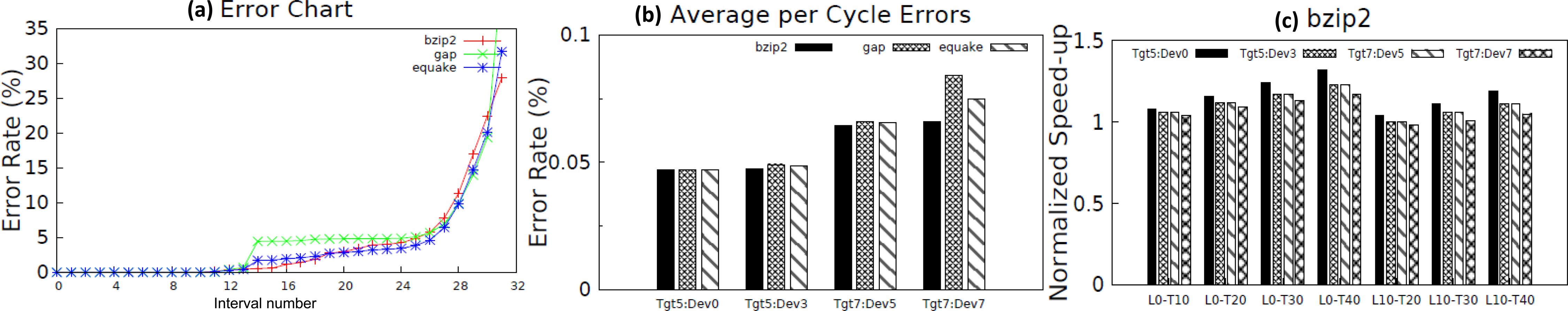
Figure 3A shows the cumulative error rate of selected SPEC 2000 workloads for 32 equal intervals, for worst-case delay of 7 ns and minimum contamination delay of 3.5 ns. The error profile obtained is the average values obtained by running the experiment for 100,000 cycles, and repeating the experiment with different sequences of 100,000 instructions for each workload. Benchmarks gap and bzip2 are core bound and therefore have a dominating timing error rate. Benchmark equake is memory bound and its timing error rate is less than the core bound applications for the entire operating frequency range.
A random timing error injector induces appropriate number of errors in SimpleScalar. Pipeline stall of one cycle per error occurrence is added correspondingly. As increasing the contamination delay affects path distribution of the whole circuit, it is likely that the overall error rate for each workload may go up. In our experiment, we assume uniform increase in error rate, denoted as Dev, for each workload. For our study, we used Dev = 0, 3, 5 and 7%. Further, we analyze the performance impact of varying CDs with different target error rates (Tgt). Figure 3B shows the error occurrence per cycle for bzip2, equake and gap. Quite evidently, we observed smaller error occurrences for small/no deviation of circuit, and the error rate tend to increase as the error rate due deviation, Dev, goes up. However, a small increase in target error rate allows more margins for performance increase. But, this may not hold true for higher error rates. In general, it was generally observed that when Dev gets closer to Tgt, there was an increase in error occurrences. This is more noticeable in the case of gap.
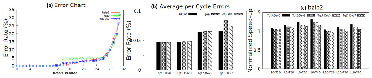
Figure 3: (A) Cumulative error rate at different clock periods for the IVM Alpha processor executing instructions from SPEC 2000 benchmarks (B) Average error rate per clock cycle (C) Normalized speed-up relative to reliably overclocked original unmodified circuit.
Since it may not always be possible to increase the contamination delay without affecting the critical paths, we increase the CD to a threshold limit. As a result, we may end up increasing the PD. We also experimented with the possibility of increasing PD by allowing a leeway of a small percentage. We study the speed-up obtained for different combinations of CD threshold and PD leeway relative to the performance of aggressive clocking framework with the original circuit. denotes l% leeway of PD and t% minimum threshold of CD. We performed our study for l = 0, 10, 20 and 30% and t = 10, 20, 30 and 40%.
We found that in all the cases, performance goes up with threshold values, which is in agreement with our intuition. In other words, increasing the short path delays provides more allowance for reliable aggressive clocking assuming a moderate target error rate occurrence. It should also be noted that allowing a leeway on critical paths induces performance overhead. Normalized speed-up trend of bzip2 workload for various modes of operation is exemplified in Fig. 3C. We have illustrated the results for the modes that yielded performance gains. The performance of bzip2 benchmark for all the configurations we implemented is shown in Fig. 4. From the point of view of leeway on PD, our investigation on relative performance is summarized as follows:
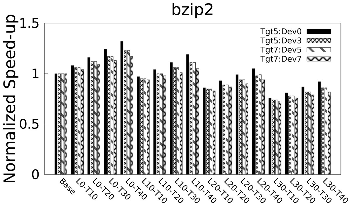
Figure 4: Normalized speed-up of bzip2 benchmark for different L and T configurations.
-
L = 0 is the best case scenario for performance benefits, yielding from 10–30% speed-up.
-
0 ≤ L ≤ 10 is the effective range for any performance benefit, irrespective of T.
-
L = 20% gives a small increase in performance in the range 0% ≤ Dev ≤ 7%.
-
L = 30% gives a little increase in performance for few cases in the range 0% ≤ Dev ≤ 5%.
-
L > 30% causes performance overhead even for higher values of T and smaller Dev.
Similar trends were observed for equake and gap as well. Our experiments reveal that by increasing the delays of short paths up to 40%, subject to moderate increase in PD (typically 10%), yields up to 30% performance enhancement. Also, it is very important to keep the increase in error rate due to circuit deviation within 5%. This guarantees zero overhead even at maximum leeway (L = 30%).
This study establishes a case for change in the existing synthesis algorithms to incorporate minimum path delay constraints. The major change in this revised algorithm is to increase the short path delays without (or minimally) affecting the critical path delays of the circuit. A secondary and passive constraint is to maintain the circuit variation (if not make it better), so that the deviation causing increase in error occurrences is kept minimal. We will discuss more on this constraint later. We provide a systematic approach to realize circuits with path delay distribution that allows greater margin for aggressive clocking for performance enhancement.
Min-arc Algorithm for Increasing Short Path Delays
It is easy to understand that increasing short path delays invariably increases the area of the circuit and, if not done carefully, affects its propagation delay. An ideal solution is to have logic moved from the critical path to the non-critical paths without using the specified components at the output terminals. This is not always possible. The next best approach would be to increase the delay of short paths as much as possible without increasing the propagation delay, and keep the area increase within a limit. As mentioned earlier, short path delays can be increased without affecting propagation delay for carry look-ahead adders and other smaller circuits. However, this is done manually, and the area overhead is very high for 64-bit adders. Minimizing short path constraints, without increasing propagation delay may not be possible for many practical circuits. In that case, we can allow a small increase in the propagation delay, if that increase can allow higher margin for TS.
We introduce Min-arc algorithm for increasing contamination delay of logic circuits up to a defined threshold. We adopt an approach closely resembling the min-cut algorithm for flow networks. The basic idea of the algorithm is to identify a set of edges, referred to as the cut-set, such that adding a fixed amount of delay to the set does not affect the delays of any long paths. However, an important difference between this and traditional flow networks is that the cut-set for the Min-arc may not necessarily break the flow of the network. But rather, the cut-set is a subset of edges in the actual (rather traditional) min-cut. The reason why we do not consider a traditional min-cut is to not unnecessarily add delay buffers where it is not needed. However, a subset of the min-cut edges is essential to keep the addition of delays minimal. Another reason for increasing the path delay in batches is to keep the structure of the logic network close to unaltered from the original network. Benefits of maintaining path delay distribution is explained further in ‘Evaluation of Min-arc Method.’
The basic outline of the Min-arc algorithm to increase the short path delay of the circuit is presented in Algorithm 1. The entire procedure is divided into six basic steps, in which the first and last steps are one-time operations, converting the logic circuit to an equivalent graph network and vice-versa. The remaining parts of the algorithm modify the graph into a weighted graph network and iteratively update the prepared network by adding the necessary delay to the selected interconnection using the modified min-cut procedure. We explain these steps in detail below.
Construction of weighted graph network
The first step is to convert the given combinational logic into a directed graph, where the logic blocks are nodes and the interconnections from each logic block to others form directed edges. The nodes and edges may be weighted depending on their time delays. To this graph we add a source, S, and edges that connects S to all the inputs. We also add a drain node, D, to which all the outputs connect. The weights for S, D and all the edges from/to them are set to zero. Figure 5 illustrates an example network model for a 4-bit ripple carry adder with S and D added. TPD and TCD of the logic circuit are highlighted in the figure. It is necessary to preserve the node types whether they are logic gates, buffer delays, input or output pins. Also it is important to note the type of logic for a logic gate node. This is important in order to maintain functional correctness of the circuit.
Finding the minimum and maximum path
Once the directed network is constructed, the next step is to mark the edge weights for generating the cut-set. We use several terms and symbols as described in Table 2. We calculate the longest and shortest distances from source to one end node of an edge and from the other end of the edge to drain. That is, we obtain MAX(S, i), MAX(j, D) MIN(S, i) and MIN(j, D) for every edge e(i, j) in the weighted graph. We use Djikstra’s algorithm to calculate MAX() and MIN() functions. From this, we calculate emax(i, j) and emin(i, j) for every edge, e(i, j) as described in Table 2, which corresponds to the longest and shortest paths of the logic network through that edge. The paths marking emin(i, j) and emax(i, j) for randomly chosen nodes i and j for the 4-bit ripple carry example is depicted in Fig. 5. In a similar manner, the minimum and maximum weights for every edge are calculated.
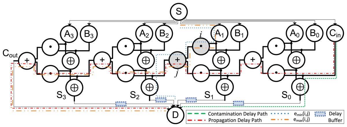
Figure 5: Illustration: network model for 4-bit ripple carry adder, assuming unit interconnect and logic delays.
| Terms | Definitions |
|---|---|
| MAX(i, j) | Maximum delay path from node i to j, incl. i and j |
| MIN(i, j) | Minimum delay path from node i to j, incl. i and j |
| MAX(S, D) | Propagation delay of the circuit, TPD |
| MIN(S, D) | Contamination delay of the circuit, TCD |
| e(i, j) | Edge from node i to j |
| wt(i, j) | Weight of edge from node i to j, not incl i and j |
| emax(i, j) | MAX(S, i) + wt(i, j) + MAX(j, D) |
| emin(i, j) | MIN(S, i) + wt(i, j) + MIN(j, D) |
| LWY | Percentage of leeway [0-1] on critical path while adding buffer. E.g., LWY = x% allows the target network to have TPD(1 + x∕100) as the final propagation delay |
| THD | Normalized threshold (from TCD to TPD) below which we do not want any short paths |
| INF | A very large integer value |
| SCALE | A moderate integer value, (>TPD), to scale the weight to a new range. |
| func() | A function dependent on TPD, TCD, emax(i, j) and emin(i, j). Returns a real number, 0-1. In this work, we define this as |
Preparing graph for min-cut
We construct a weighted graph network to select a minimum weight interconnection to add the delay buffer. Once we add a delay buffer, we recalculate new edge weights. The edge weights are calculated in such a manner that the minimum weighted arc gives the most favorable interconnection where to add delay. The procedure for calculating new weights for every edge, e(i, j), is described in Algorithm 2. The edge, e(i, j) may fall under one of the four categories listed in the algorithm. For the first two cases, the edge weight is calculated as the sum of emin(i, j) and emax(i, j). This is the general scenario where the minimum and maximum paths are added as edge weights. The first case is the scenario of a short path, where emax(i, j) is smaller than the threshold for contamination delay. The latter case is when the selected edge, e(i, j), has a delay such that the shortest path is closer to the threshold than the longest path is to the propagation delay. In other words, when a delay buffer is added to any edge in the path to increase the short path delay by the given threshold, the maximum delay increase affecting a critical path is still within propagation delay of the circuit. The third scenario is when the longest path exceeds propagation delay including leeway. This edge is critical and by no means any buffer can be added to this. Hence, we assume a large number (INF) as the edge weight so that this edge is never picked as part of the min-cut. Finally, we have a case when delay buffer addition exceeds or gets very close to the propagation delay. In this case, we scale the edge weight moderately higher than the original range. This addresses the case where addition of buffer to this edge affects longer paths.
Finding the min-cut
Once the edge weights are re-assigned, the cut-set is determined. We use a variant of Edmonds−Karp min-cut algorithm for graph network (Edmonds & Karp, 1972). The cut-set consists of edges with minimum weight in the graph with assigned weights. Figure 6 illustrates the different scenarios in determining the cut-set. The cut-set re-definition is necessary because the traditional min-cut always has at least one edge in the critical path. Figure 6A shows how a logic circuit is divided into critical and non-critical paths. As long as the non-critcical paths are independent of critical paths, buffer delays can be added to the former ones. In this case, the min-cut excludes all the critical paths. Generally, the scenario is not this straightforward. As illustrated in Fig. 6B, the short paths are intertwined with longer paths that are not critical paths. In such cases, the weights of the longer paths are scaled to a different range (in this case K). If there is a subset of short paths that exist independent of the longer paths, buffer delays are added to this subset. We noticed that this is the most common scenario in the benchmark circuits. Once all the independent short paths have been added with corresponding delays, the new circuit is left out with paths that are scaled as shown in Fig. 6C. Buffer delay is added to the scaled paths, which runs the risk of modifying longer paths into critical paths. The final circuit is shown in Fig. 6D, where there are only critical paths and paths that have delay meeting the threshold requirements. In the ripple carry example, the case is similar to Fig. 6A. The cut-set is thus all the paths excluding the critical path. Figure 5 also shows the min-cut where the buffers are added.
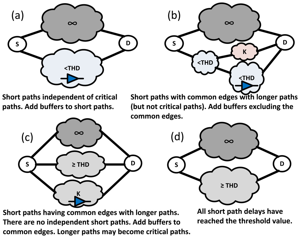
Figure 6: Illustration of four different scenarios finding the cut-set in Min-arc algorithm.
Adding buffer delays
The buffers are carefully placed on edges where they would not affect the longest paths. Thus, the amount of delay each buffer adds depend on the path connectivity, which may have major impact on the timing error occurrence. For example, it is possible to add delays such that all the paths have delay equal to the critical path delay. In most practical circuits, increasing all path delays to a certain delay interval can result in a rise in the timing errors, causing overhead due to error recovery. Thus, it is always necessary to keep this under control when designing the algorithm so that there is a gentle rise in path delays from one interval to the other. Buffers are added on the edges present in the cut-set. The amount of delay added, delay(i, j), for any edge e(i, j) is given by Eq. (7). (7)
The delays for all the edges in a cut-set, for a given iteration, are added at the same time. While adding delay, we ensure that in one iteration there are no other edges to which the delay is added that are connected to paths through this edge. Please note that there is a relation between max-flow and min-cut problems and the proposed formulation is in fact max-flow.
Satisfying conditions
We iterate steps B through F until the minimum condition for the shortest path is met or until there is no other edge where delay can be added without affecting TPD of the circuit (including LWY). Step F checks if the desired value of contamination delay is reached. Once the required conditions are met, no more buffers can be added and the algorithm moves on to step G. From our experiments, we found that the minimum condition for contamination delay is achieved for all the circuits we evaluated.
Converting graph to logic circuit
The final step is to revert back to the original circuit once the short paths lengths are increased to the desired level. Since we record the node types in the network graphs in step A, it is possible to re-build the circuit from the graph network with the added buffers. It should be noted that we do not modify the logic of the circuit, as we only add additional buffers preserving the original logic of the circuit.
Complexity of Min-arc algorithm
The time complexity of Min-arc algorithm is mainly affected by Steps B and D. Let |V| be the total number of logic blocks (vertices) and |E| is the total number of interconnections (edges) in the logic circuit. Using Djikstra’s shortest path algorithm, the worst case time to calculate MAX() and MIN() functions is O(|V|2). For finding the minimum weighted edge min-cut for the graph network, it takes O(|V ∥ E|2). In the worst case every edge becomes a part of the cut-set. That is, there are at most |E| iterations. Hence, the overall time complexity of the Min-arc algorithm is O(|V|2|E| + |V ∥ E|3), which is dominated by the second term as |V| < |E|.
Impact of process variation
Process variation can alter gate delays and hence can alter the distribution of path delays. Therefore, we need to take conservative estimates of circuit delays into account while using our algorithm. Inter-die variations impact all the paths and therefore impact on our algorithm is minimal. To mitigate intra-die variation, conservative padding of buffers needs to be done on the short paths to make sure that extreme variation is tolerated at the expense of area overhead. If such additional area overheads are to be ignored, process variation will only reduce the range of aggressive clocking slightly; and cannot eliminate the possibility of reliable overclocking and the scope for performance improvement by TS. Given that the scope of this paper is to demonstrate the concept and develop an algorithm to realize it, we do not evaluate the actual impact any further.
Evaluation of Min-arc method
Although the time complexity of Min-arc algorithm is polynomial order, it is necessary to consider its performance on practical circuits. We evaluate the algorithm on ISCAS’85 benchmark suite (Hansen, Yalcin & Hayes, 1999). The suite provides a diverse class of circuits in terms of number of IOs, logic gates and interconnections (nets). Table 3 lists a brief description and other relevant details of the circuits. All the circuits were transformed into network graphs as described in ‘Min-arc Algorithm for Increasing Short Path Delays’. The interconnect delays and logic cell delays were obtained by synthesizing the circuits for 45 nm technology using OSU standard cell library (Stine et al., 2007). All circuits are synthesized for minimum area (max area is set to zero) using Synopsys Design Compiler, which acts as a starting point for our algorithm. All the configurations () described in ‘Performance & Contamination Delay: A Study on Alpha Processor’ were investigated.
| Circuit | Description | Inputs | Outputs | Gates | Nets | Area (µm2) |
|---|---|---|---|---|---|---|
| c432 | 27-channel interrupt controller | 36 | 7 | 205 | 386 | 5,361 |
| c499 | 32-bit SEC circuit | 41 | 32 | 277 | 513 | 7,821 |
| c880 | 8-bit ALU | 60 | 26 | 471 | 841 | 11,792 |
| c1355 | 32-bit SEC circuit | 41 | 32 | 621 | 1,169 | 17,167 |
| c1908 | 16-bit SEC/DED circuit | 33 | 25 | 940 | 1,581 | 24,948 |
| c2670 | 12-bit ALU and controller | 233 | 140 | 1,644 | 2,665 | 36,016 |
| c3540 | 8-bit ALU | 50 | 22 | 1,743 | 3,033 | 49,140 |
| c5315 | 9-bit ALU | 178 | 123 | 2,610 | 4,810 | 71,726 |
| c7552 | 32-bit adder/comparator | 207 | 108 | 3,830 | 6,568 | 10,1953 |
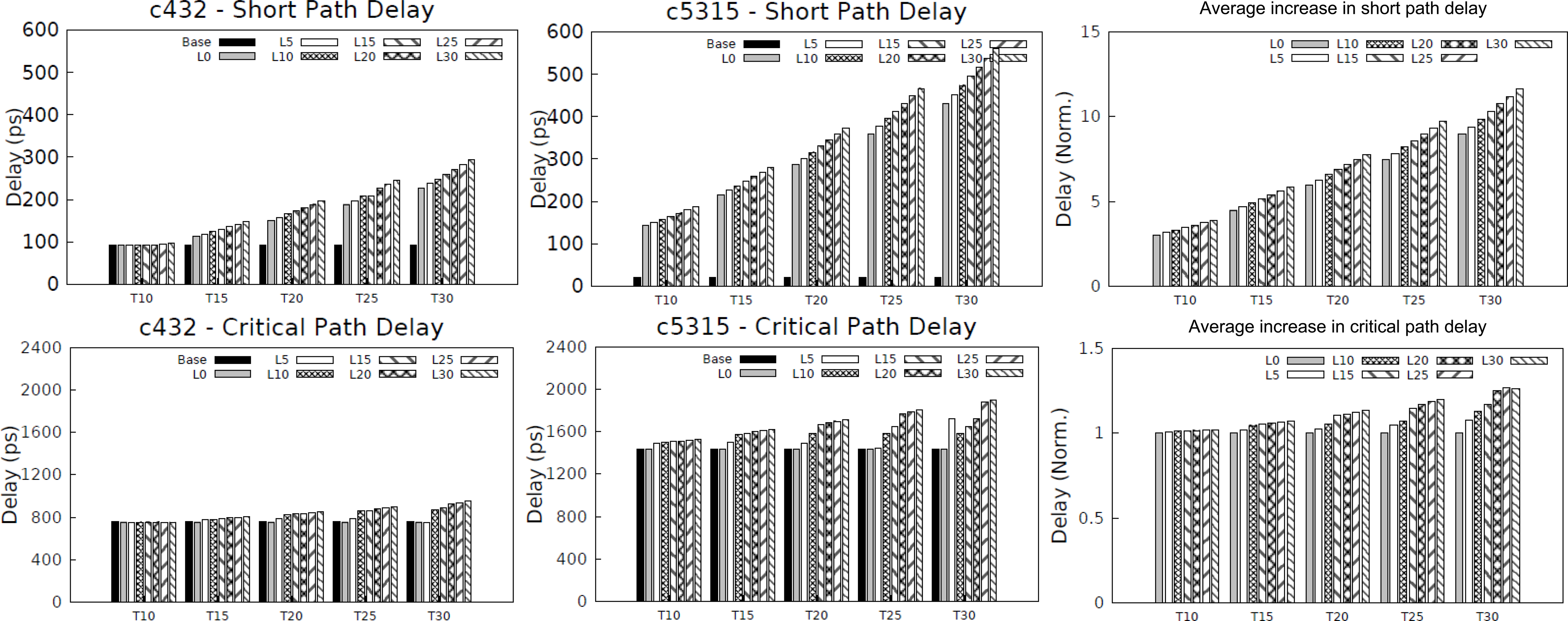
Figure 7: Charts showing increase in contamination (short path) delay and propagation (critical path) delay of circuits.
Results analysis
Positive results were noted in this study. First, for all the circuits, the Min-arc method was able to increase the short path delays to the desired threshold levels without any leeway on PD. We continued our evaluation with all the configurations to include leeway in order to study the effect of increasing PD. We include the results only for a few selected circuits and average of all circuits. It was found that circuit characteristics (i.e., size and connectivity) have strong effects on how the algorithm performs. Figure 7 illustrates the increase in the short path delays and critical path delays for different configuration in c432 and c5315 circuits. The chart also shows the average increase of short and critical path delays for all nine circuits. For smaller circuits (as in c432), we notice that there is not much the algorithm possibly could do, as there is a higher chance of affecting the critical path by adding delay to any net. In c432, we notice that the maximum delay increase of short paths from the base circuit with 91 ps, (with 0% leeway) is around 225 ps. However, in larger circuits (as in c5315), delay buffers were more easily added. This is seen in c5315, where short path delay is increased from 20 ps to 430 ps, again with 0% leeway. In other words, as the circuit size increases, the number of independent short paths also become higher in number, allowing easy inclusion of delay buffers.
It should also be noted that there is not much impact on increasing leeway from L0 to L5 or even higher levels PD. On the other hand, increasing leeway tend to have a great impact in increasing the CD. On an average, there is a 1.5 × factor of increase in short path delay for each 5% increase in leeway. Assuming LWY = 0, we were able to achieve 300%–900% increase in CD, and increasing LWY steadily from 5 to 30%, we observed increase of CD in a saw tooth pattern achieving 315%–1,165% increase in CD. It should be observed from the critical path delay patterns that the algorithm strictly adheres to the limit imposed on critical path delay.
One major side effect of adding buffers to circuits is that it affects path delay distribution. Although our goal is to increase the CD to a threshold limit, pushing a set of paths to one side may increase the timing error rate during execution. Therefore, it is important to analyze the delay distribution of the circuit paths. Even though the structure of the circuit is maintained, as the short paths are now pushed to offer higher delay, it increases the possibility of error occurrences in TS framework. For our case study in ‘Performance & Contamination Delay: A Study on Alpha Processor,’ we modelled this increase in timing error rates as Dev.
Figure 8 illustrates the path delay distributions for selected configurations of two circuits (c432 and c7552). We have divided the range between CD and PD into ten bins. X-axis in Fig. 8 represent the bin number. For c432, T30L0 and T30L5 configuration reduce the number of paths having higher delay. This implies a reduction in timing error rate in TS framework. Higher leeway configuration T30L30 increases CD but path delay distribution matches the base line, implying no increase in timing error rate. For c7552, even no leeway configuraion (T30L0) performs better than baseline. Also, higher leeway configurations, T30L5 and T30L30, perform much better than baseline in terms of paths having higher delay. Overall, for c432 (and other smaller circuits), the path structure is mostly maintained and in the case of c7552 (and otherlarger circuits), the circuit structure was altered moderately. Increase in number of paths having higher delay implies increase in timing error rate of TS framework. From these results, we conclude that for smaller circuits, our algorithm maintains or does not increase timing error rate of TS framework. For larger circuits, our algorithm reduces the timing error rate for higher leeway configurations. As timing error rate also influence the possible performance gain, reduction in timing error rate is favorable for TS framework.
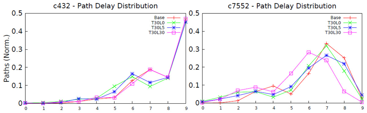
Figure 8: Path delay distribution from CD to PD for c432 and c7552.
To illustrate this point further, we present mean and standard deviation of all the circuits. Figure 9 presents plots of selected circuits and average of all the circuits. We note that the smaller circuits (c432) suffer from negligible deviation from original circuit in spite of higher mean, and the larger circuits ((c7552)) are vulnerable to change in structure. From the average plot, it is also evident that higher leeway values cause more deviation. A maximum deviation of −12% and +16% were observed for T30L0 and T30L30 configurations, respectively.
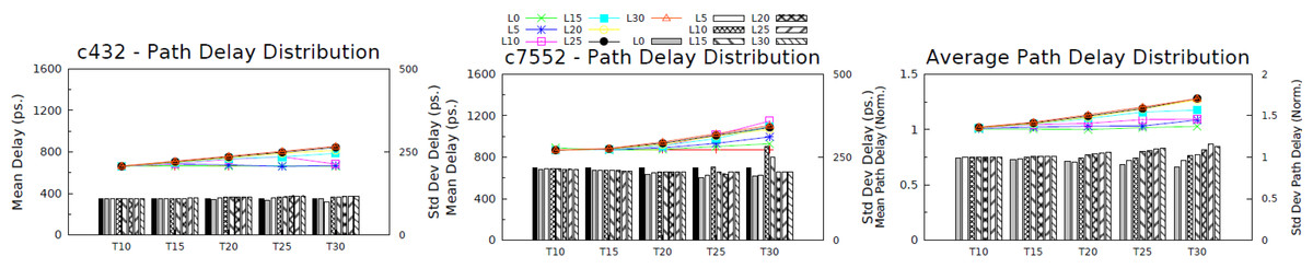
Figure 9: Average path delay distribution, in terms of mean and deviation.
Mean values are represented by line while standard deviation values are represented by bars.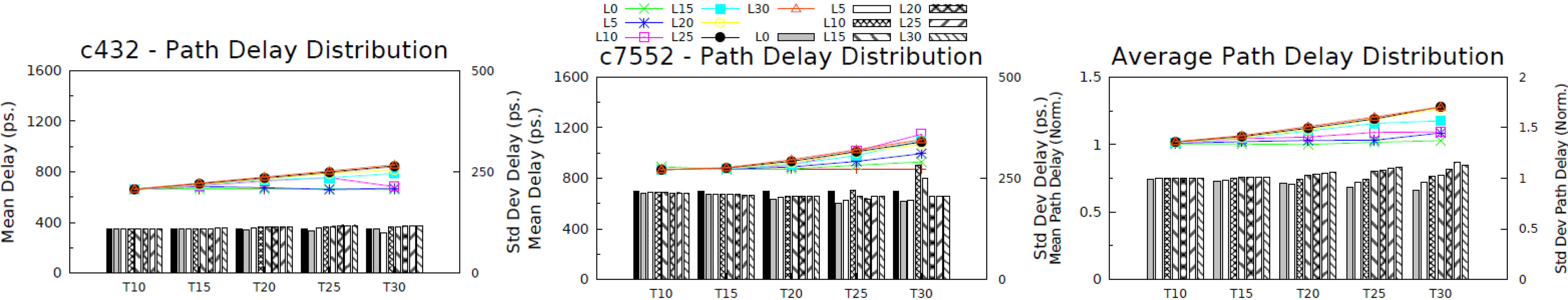
Area overhead
A major overhead for Min-arc algorithm is the area penalty. More the circuit allows adding buffers, more the overhead in chip real estate. We estimate the original circuit area in terms of buffer delays, and compare the area increase for each of the configurations. This study facilitates to narrow down the choices of L and T for any given circuit. Table 4 enlists the percentage area increase for various L and T combinations, for all the circuits. It is important to choose the configuration that has highest increase in delay with moderate increase in area.
Without any leeway (corresponding to L0), with every 5% increase in T there is around 20% increase in area. This holds for most circuits, except for smaller circuits as in c499 and c880, where it is around 10%. A maximum of 100% increase is observed for c2670 at T = 30%. For this maximum threshold, there is a wide range of area increase across the benchmark circuits. We did not observe any strong relation between circuit size and the area increase. This means that it is the circuit connectivity that has a major role to play on buffer placements. For T = 30%, the minimum area increase of around 10% is observed for the circuit c3540.
A general observation from our study is that the area increases with L or T. However, we did observe quite a few configurations, where the area decreases with L or T. This reflects how the algorithm handles different input combinations independently, rather than building from previous level output. We noticed several places where area would decrease with L (shaded dark black in Table 4). Observation related to these shaded entries is that they beat the increasing area trend with increasing leeway. As illustrated, there is at least one place where this occurs in each circuit, with the exception of c499 and 2670. In the case of T, we notice that there are only a couple of configurations where this occurs, namely in c3540 (underlined in Table 4). This explains how target threshold for short paths affect increase in area. In most cases, we noticed around 2% increase in area for every 5% in L. In majority of the cases, we noted only moderate increase in area (<50%). We observed 12 cases where the area increase was more than 100%, in which 10 of them are from the same circuit, c2670. This is a 12-bit ALU with controller (c2670) that has a lot of parallel paths with few common edges. Similar but less intense effect is seen in the case of the 9-bit ALU (c5315). The configurations where the area increase exceeds 100% is highlighted light black in the table.
Power overhead
The addition of buffers to the circuit for increasing contamination delay also increases the power consumption. Table 5 presents the percentage power increase for various L and T combinations. Using the spice models, we have estimated the power consumed by the buffers added and estimated the percentage increase in worst case power consumption. We have used golden configuration (L0T0) as the base for all configurations of L and T.
| Ckt | L0 | L5 | L10 | L15 | L20 | L25 | L30 | |
|---|---|---|---|---|---|---|---|---|
| c432 | T10 | 0.0 | 0.0 | 0.0 | 0.0 | 0.0 | 0.1 | 0.3 |
| T15 | 2.2 | 1.9 | 2.3 | 2.7 | 3.1 | 3.6 | 4.0 | |
| T20 | 10.9 | 14.4 | 5.7 | 6.4 | 7.2 | 8.0 | 8.9 | |
| T25 | 27.9 | 34.7 | 10.9 | 12.1 | 12.2 | 13.4 | 14.6 | |
| T30 | 55.9 | 62.2 | 70.7 | 19.9 | 20.0 | 19.5 | 21.0 | |
| c499 | T10 | 1.3 | 2.3 | 3.3 | 4.2 | 5.3 | 6.2 | 7.2 |
| T15 | 11.1 | 12.6 | 14.1 | 15.6 | 17.0 | 18.6 | 20.0 | |
| T20 | 21.0 | 22.9 | 24.9 | 26.9 | 28.9 | 30.8 | 32.8 | |
| T25 | 30.8 | 33.3 | 35.7 | 38.2 | 40.7 | 43.1 | 45.6 | |
| T30 | 40.6 | 43.6 | 46.5 | 49.5 | 52.4 | 55.4 | 58.3 | |
| c880 | T10 | 0.9 | 1.1 | 1.3 | 1.7 | 2.0 | 2.4 | 2.8 |
| T15 | 4.6 | 5.4 | 6.2 | 6.9 | 7.8 | 8.8 | 9.9 | |
| T20 | 13.3 | 15.1 | 13.6 | 15.3 | 17.1 | 18.8 | 20.6 | |
| T25 | 25.0 | 35.4 | 23.2 | 25.4 | 27.6 | 29.7 | 31.9 | |
| T30 | 32.7 | 37.8 | 49.3 | 35.4 | 38.0 | 40.6 | 43.3 | |
| c1355 | T10 | 0.0 | 0.1 | 0.9 | 1.6 | 2.4 | 3.2 | 3.9 |
| T15 | 7.9 | 9.6 | 9.2 | 10.3 | 11.5 | 12.6 | 13.7 | |
| T20 | 23.0 | 26.0 | 29.0 | 19.0 | 20.5 | 22.0 | 23.5 | |
| T25 | 38.0 | 41.8 | 45.6 | 27.7 | 29.6 | 31.4 | 33.3 | |
| T30 | 53.2 | 57.7 | 62.2 | 36.3 | 39.3 | 40.9 | 43.1 | |
| c1908 | T10 | 3.1 | 3.7 | 4.3 | 4.9 | 5.5 | 6.1 | 6.7 |
| T15 | 8.1 | 9.9 | 10.8 | 11.7 | 12.6 | 13.5 | 14.4 | |
| T20 | 15.4 | 16.1 | 18.3 | 18.5 | 19.7 | 20.9 | 22.1 | |
| T25 | 24.7 | 25.1 | 27.1 | 28.9 | 26.9 | 28.3 | 29.8 | |
| T30 | 35.2 | 35.9 | 35.9 | 37.9 | 40.2 | 44.1 | 37.5 | |
| c2670 | T10 | 23.4 | 25.1 | 26.8 | 28.6 | 30.4 | 32.1 | 34.0 |
| T15 | 41.6 | 44.5 | 47.4 | 50.4 | 53.3 | 56.3 | 59.2 | |
| T20 | 60.5 | 64.6 | 69.0 | 73.0 | 77.0 | 81.0 | 85.0 | |
| T25 | 81.1 | 88.3 | 92.1 | 95.9 | 100.9 | 105.9 | 110.8 | |
| T30 | 100.5 | 117.6 | 113.2 | 132.3 | 131.6 | 138.1 | 136.9 | |
| c3540 | T10 | 0.6 | 0.7 | 0.8 | 0.9 | 1.0 | 1.0 | 1.1 |
| T15 | 2.0 | 2.8 | 2.7 | 3.1 | 3.5 | 3.9 | 4.3 | |
| T20 | 5.4 | 5.2 | 7.7 | 6.4 | 7.0 | 7.6 | 8.2 | |
| T25 | 7.7 | 17.6 | 9.9 | 13.9 | 15.1 | 11.4 | 12.2 | |
| T30 | 10.8 | 15.6 | 19.5 | 13.4 | 45.0 | 21.4 | 27.4 | |
| c5315 | T10 | 7.9 | 11.7 | 12.8 | 14.0 | 15.1 | 16.3 | 17.5 |
| T15 | 24.6 | 25.7 | 25.8 | 27.6 | 29.4 | 31.2 | 33.0 | |
| T20 | 39.8 | 42.6 | 41.6 | 41.6 | 44.1 | 46.5 | 49.0 | |
| T25 | 63.5 | 66.1 | 58.3 | 56.1 | 58.8 | 61.9 | 65.0 | |
| T30 | 74.3 | 102.9 | 085.1 | 107.3 | 95.2 | 77.3 | 81.0 | |
| c7552 | T10 | 5.4 | 5.5 | 5.9 | 6.2 | 6.7 | 7.1 | 7.5 |
| T15 | 9.4 | 10.2 | 11.1 | 11.9 | 12.8 | 13.7 | 14.6 | |
| T20 | 15.3 | 16.5 | 17.8 | 19.0 | 20.2 | 21.5 | 22.9 | |
| T25 | 22.6 | 26.0 | 26.9 | 26.4 | 29.2 | 29.6 | 31.2 | |
| T30 | 40.3 | 39.2 | 43.6 | 41.7 | 35.7 | 37.7 | 39.6 |
| Ckt | L0 | L5 | L10 | L15 | L20 | L25 | L30 | |
|---|---|---|---|---|---|---|---|---|
| c432 | T10 | 0.0 | 0.0 | 0.0 | 0.0 | 0.0 | 0.2 | 0.5 |
| T15 | 2.2 | 1.9 | 2.2 | 2.7 | 3.1 | 3.4 | 3.9 | |
| T20 | 10.4 | 13.5 | 5.5 | 6.0 | 6.7 | 7.7 | 8.4 | |
| T25 | 26.3 | 32.5 | 10.4 | 11.6 | 11.6 | 12.5 | 13.7 | |
| T30 | 52.3 | 58.3 | 66.3 | 18.8 | 18.8 | 18.3 | 19.8 | |
| c499 | T10 | 0.4 | 0.8 | 1.1 | 1.5 | 1.8 | 2.1 | 2.5 |
| T15 | 3.8 | 4.3 | 4.7 | 5.3 | 5.7 | 6.2 | 6.7 | |
| T20 | 7.1 | 7.7 | 8.3 | 9.0 | 9.6 | 10.3 | 11.0 | |
| T25 | 10.3 | 11.1 | 12.0 | 12.8 | 13.5 | 14.4 | 15.2 | |
| T30 | 13.5 | 14.6 | 15.6 | 16.6 | 17.5 | 18.5 | 19.5 | |
| c880 | T10 | 0.3 | 0.4 | 0.5 | 0.7 | 0.8 | 0.9 | 1.0 |
| T15 | 1.6 | 2.0 | 2.2 | 2.5 | 2.8 | 3.2 | 3.5 | |
| T20 | 4.7 | 5.3 | 4.8 | 5.5 | 6.0 | 6.7 | 7.3 | |
| T25 | 8.8 | 12.4 | 8.2 | 8.9 | 9.7 | 10.5 | 11.2 | |
| T30 | 11.6 | 13.3 | 17.3 | 12.4 | 13.4 | 14.3 | 15.3 | |
| c1355 | T10 | 0.0 | 0.1 | 0.3 | 0.5 | 0.9 | 1.1 | 1.3 |
| T15 | 2.6 | 3.2 | 3.1 | 3.4 | 3.8 | 4.2 | 4.5 | |
| T20 | 7.6 | 8.5 | 9.5 | 6.2 | 6.7 | 7.2 | 7.7 | |
| T25 | 12.5 | 13.7 | 14.9 | 9.1 | 9.6 | 10.3 | 10.9 | |
| T30 | 17.4 | 18.8 | 20.4 | 11.9 | 12.9 | 13.4 | 14.1 | |
| c1908 | T10 | 0.6 | 0.7 | 0.8 | 0.9 | 1.0 | 1.1 | 1.2 |
| T15 | 1.4 | 1.8 | 2.0 | 2.1 | 2.3 | 2.4 | 2.6 | |
| T20 | 2.8 | 2.9 | 3.4 | 3.4 | 3.6 | 3.8 | 4.0 | |
| T25 | 4.5 | 4.6 | 4.9 | 5.2 | 4.9 | 5.1 | 5.4 | |
| T30 | 6.3 | 6.5 | 6.5 | 6.9 | 7.2 | 7.9 | 6.8 | |
| c2670 | T10 | 3.8 | 4.1 | 4.4 | 4.7 | 4.9 | 5.2 | 5.5 |
| T15 | 6.8 | 7.3 | 7.7 | 8.2 | 8.7 | 9.2 | 9.6 | |
| T20 | 9.9 | 10.5 | 11.2 | 11.9 | 12.5 | 13.2 | 13.8 | |
| T25 | 13.2 | 14.4 | 15.0 | 15.6 | 16.4 | 17.2 | 18.0 | |
| T30 | 16.4 | 19.1 | 18.4 | 21.5 | 21.4 | 22.5 | 22.3 | |
| c3540 | T10 | 0.5 | 0.6 | 0.6 | 0.7 | 0.7 | 0.8 | 0.9 |
| T15 | 1.5 | 2.1 | 2.0 | 2.3 | 2.6 | 2.9 | 3.2 | |
| T20 | 4.0 | 3.9 | 5.7 | 4.8 | 5.2 | 5.7 | 6.1 | |
| T25 | 5.7 | 13.1 | 7.4 | 10.4 | 11.2 | 8.5 | 9.1 | |
| T30 | 8.0 | 11.6 | 14.5 | 10.0 | 33.5 | 15.9 | 20.4 | |
| c5315 | T10 | 3.4 | 5.0 | 5.5 | 6.0 | 6.5 | 7.0 | 7.5 |
| T15 | 10.5 | 11.0 | 11.0 | 11.8 | 12.5 | 13.3 | 14.1 | |
| T20 | 16.9 | 18.1 | 17.7 | 17.7 | 18.8 | 19.9 | 20.9 | |
| T25 | 27.1 | 28.2 | 24.9 | 23.9 | 25.1 | 26.4 | 27.7 | |
| T30 | 31.7 | 43.9 | 36.3 | 45.7 | 40.6 | 33.0 | 34.5 | |
| c7552 | T10 | 2.3 | 2.3 | 2.5 | 2.6 | 2.8 | 3.0 | 3.2 |
| T15 | 4.0 | 4.3 | 4.7 | 5.0 | 5.4 | 5.8 | 6.1 | |
| T20 | 6.5 | 6.9 | 7.5 | 8.0 | 8.5 | 9.1 | 9.6 | |
| T25 | 9.5 | 10.9 | 11.3 | 11.1 | 12.3 | 12.5 | 13.1 | |
| T30 | 17.0 | 16.5 | 18.4 | 17.6 | 15.0 | 15.9 | 16.7 |
We notice from the table that increase in power consumption is also dependent on the circuit topology rather than the size of the circuit. Without any leeway (corresponding to L0), with every 5% increase in T there is only around 4% increase in power. This holds for most circuits, except for smaller circuit c432. We also notice that for a given T, increasing L has very minimal effect (2%–3%) on the power increase. Therefore, while applying our algorithm, an optimal value of T can be chosen as any value of L can be chosen without altering the power budget.
When timing speculation is used for overclocking, voltage is kept constant. Therefore, increase in power is independent of voltage and is dependent only on frequency change and the additional power overhead caused by the buffers. In this paper, as we primarily analyze our algorithm at circuit-level, we only present power results at circuit-level. Changes in system-level power estimates can be easily derived with the power analysis present in this section. When compared to area overheads of our algorithm, power results presented in Table 5 are quite interesting. For example, for circuit c2670 where we have seen 100% area increase, power increase is only about 16%. The power increase is relatively small when compared to the area increase. It is due to the fact the delay buffers draw much less current than the other standard cells. Even though we are limited with the type of delay buffer configurations available in our cell library, much more complex buffers can be constructed at gate-level which can consume less power without degrading delay characteristics.
Related Literature
Early works on timing verification involved identification and categorization of long paths as either false paths or sensitizing paths (Du, Yen & Ghanta, 1989). Long paths that are false paths (paths with no activity) unnecessarily increase the circuit critical delay. Therefore, detecting false paths and mitigating them is a critical issue in digital circuits even to this day (Cheng et al., 2007; Tsai & Huang, 2009; Coudert, 2010).
As already mentioned in ‘Introduction,’ not many works are done keeping short paths in mind. Sylon-Dream accomplishes faster multi-level networks by its level reduction technique (SDLR) (Chen & Muroga, 1991). The non-critical paths are processed by an area reduction procedure to reduce network area without increasing the maximum depth. SDLR uses the concept of permissible functions in both level and area reduction procedures. Gate resizing and buffer insertion are two major techniques for critical path optimization. Critical path selection instead of sensitization is suggested for performance optimization (Chen, Du & Liu, 1993). Here the objective is to select a small set of paths to ease the optimization process by guaranteeing the delay of the circuit to be no longer than a given threshold. Several optimization techniques, involving clustering, logic analysis and gate resizing are proposed in Touati, Savoj & Brayton (1991), Rohfleisch, Wurth & Antreich (1995), Entrena et al. (1996), Fang & Jone (1995) and Lu et al. (1998). A statistical timing analysis approach is investigated in Jyu & Malik (1993). A re-timing and re-synthesis approach is presented in Pan (1999). This work suggests re-synthesizing the circuit to expose signal dependencies. The optimization scheme tightly constrains logic re-synthesis, so that the re-synthesized circuit is guaranteed to meet the performance target. Recent work in Kim, Joo & Kim (2013) focus on buffer insertion to solve variation in clock skew. The authors in Lin, Lin & Ho (2011) explore adjustable delay buffer insertion for minimizing clock skew in multi voltage designs. Buffer insertion in the presence of process variation is explored in Xiong & He (2006) with the focus on improving yield.
The authors in Dynatune propose an algorithm based on min-cut approach to shorten the long path delay (Wan & Chen, 2009). It is based on simulation profiling and uses multiple threshold voltage cells to reduce the delay of long paths. Even though our min-cut algorithm is similar to the Dynatune algorithm, it is applied to a drastically different aspect of timing speculation framework i.e., increasing contamination delay. Unlike Dynatune, our approach doesn’t use simulation profiling to drive the circuit optimization as hold time delay should be satisfied all the time. Therefore, our algorithm considers more tighter constraints than the Dynatune algorithm.
Although there are several delay optimization approaches proposed in literature, all of them try to hold the critical path delay within a threshold. It is fundamental that all the timing optimization algorithms must consider short path timing constraints. Data latches in a pipelined architecture inherently possess set up and hold time constraints. It is necessary to make sure that the resulting circuit has no set-up or hold time violations, to guarantee correct data transfers. There are algorithms to make sure the circuit is free of any such violations considering both long and short paths (Fung, Betz & Chow, 2004). However, there is no consideration for short path constraints from the perspective of aggressive clocking we are dealing with.
The authors in Ye et al. (2015) propose a steepest descent method (SDM) to determine the potential benefits of timing speculation. From the experiments conducted, it is found that circuit topology plays a big role in realizing the benefits of timing speculation. Our algorithm can be used for circuits that shows promising results using SDM approach analyzed with design parameters like process technology, desired frequency and voltage corners, error penalty of the implementation etc. In this paper, we try to alleviate the contamination delay limitation imposed on aggressive timing speculation architectures. Due to this, we fundamentally differ from all of the existing works. This is the first work aimed at increasing the contamination delay of digital circuits up to a given threshold. It is also important to point out that our algorithm works complementary to existing synthesis schemes and can also be integrated with physically aware timing optimizations that are used for achieving timing closure.
Conclusions
Contamination delay is one of the major bottlenecks for achieving higher performance in timing speculation architectures. In this paper, we investigated the theoretical margins for improving performance for the dual latch framework. We brought forward the limits to performance enhancements in timing speculation. Using our analysis, we demonstrated how much performance improvement is achievable by increasing the contamination delay of the circuit without affecting the critical path delays. Performance gains were attained even for the cases affecting propagation delay by up to 10%. We studied further how these gains vary with target timing error rate.
The main goal of this paper is to increase the short path delays to a specified threshold, without (or minimally) affecting the critical path delays. We proposed the Min-Arc algorithm to achieve this goal. We studied ISCAS-85 circuits, where we have shown that the Min-Arc is able to increase the contamination delay of all the circuits without affecting propagation delay. We analyzed further as to how much these short paths increase while allowing a small leeway to critical path delay. We observed moderate area and power increase in the circuits implementing the Min-arc algorithm. Finally, we discuss how the algorithm preserves the path delay distributions of the circuits and therefore, closely maintaining the rate of timing error occurrences from the original circuit. As a future improvement, gate/cell sizing approach can be used instead of adding delay buffers for improved area, power results. To conclude, Min-arc algorithm successfully increases the contamination delay of logic circuits with moderate area and power overheads. The results we have obtained are very promising, opening up different directions for the near future.