Article

Origin of Giant Rashba Effect in Graphene on Pt/SiC

1
Department of Physics, Saint Petersburg State University, 198504 St. Petersburg, Russia
2
School of Physics, Harbin Institute of Technology, Harbin 150001, China
3
Helmholtz-Zentrum Berlin für Materialien und Energie, 12489 Berlin, Germany
4
Resource Center “Physical Methods of Surface Investigation”, Research Park, Saint Petersburg State University, 198504 St. Petersburg, Russia
5
Donostia International Physics Center, 20018 Donostia-San Sebastián, Spain
6
Laboratory of Electronic and Spin Structure of Nanosystems, Saint Petersburg State University, 198504 St. Petersburg, Russia
*
Authors to whom correspondence should be addressed.
Symmetry 2023, 15(11), 2052; https://doi.org/10.3390/sym15112052
Submission received: 11 October 2023 / Revised: 5 November 2023 / Accepted: 10 November 2023 / Published: 12 November 2023
(This article belongs to the Section Physics)

Abstract

:
Intercalation of noble metals can produce giant Rashba-type spin–orbit splittings in graphene. The spin–orbit splitting of more than 100 meV has yet to be achieved in graphene on metal or semiconductor substrates. Here, we report the p-type graphene obtained by Pt intercalation of zero-layer graphene on SiC substrate. The spin splitting of ∼200 meV was observed at a wide range of binding energies. Comparing the results of theoretical studies of different models with the experimental ones measured by spin-ARPES, XPS and STM methods, we concluded that inducing giant spin–orbit splitting requires not only a relatively close distance between graphene and Pt layer but also the presence of graphene corrugation caused by a non-flat Pt layer. This makes it possible to find a compromise between strong hybridization and increased spin–orbit interaction. In our case, the Pt submonolayer possesses nanometer-scale lateral ordering under graphene.

1. Introduction

Induced spin–orbit coupling in graphene is still an actively investigated topic, since it opens a way to realize quantum Hall effects in graphene [1,2,3,4]. It is known that strong spin–orbit coupling is a necessary condition for observing spin Hall effects, the quantum anomalous Hall effect, the spin galvanic effect, the spin Edelstein effect, the giant Rashba effect, spin-transfer and spin–orbit torque effects, spin interference effect, etc. Various approaches can be used to enhance spin–orbit coupling in graphene and graphene-like materials. Recently, it was reported that curvature-induced spin–orbit coupling in rippled graphene structures opens a broad avenue for spintronic applications in graphene-based nanodevices [5]. Other ways to tune spin–orbit coupling are the so-called spin–orbit proximity effects with adatoms or the substrate [6,7,8,9] and the symmetry breaking in 2D Janus materials [10,11,12].
Giant Rashba splitting in graphene on the Au monolayer was reported earlier in several experimental papers [7,13,14,15,16], and was clearly supported by the density functional theory (DFT) calculations of the Gr/Ni system with intercalated Au clusters [15] and tight-binding calculations of graphene on top of a gold monolayer in the hcp configuration [17]. The giant spin splitting was observed for Au-intercalated graphene on SiC substrate [14], but authors concluded that sizable spin splittings become giant (∼100 meV) only near the avoided-crossing gap. Recently, Rashba-type spin–orbit coupling was revealed for graphene on several Co monolayers with out-of-plane magnetization but also of ∼100 meV [18].
At the same time, platinum is the most used nonmagnetic metal in spintronics because it is characterized by spin-polarized 5 d states at the Fermi level, resulting in a high intrinsic spin Hall effect [19]. Furthermore, it was shown that the graphene monolayer on the Pt(111) surface [13] and on Ir(111) with an intercalated Pt monolayer between graphene and Ir [20] exhibits pronounced spin-polarized Dirac cone-like π states.
However, graphene on metal substrates cannot be directly applied to future electronics or spintronics. In this regard, graphene systems on semiconductor substrates, such as graphene on silicon carbide (SiC) with intercalated metal, are more promising for applications [21,22,23,24,25,26,27]. The possibility of the intercalation of noble metals underneath graphene on SiC, such as Au and Pt, was shown in Refs. [14,22,23,28]. Also, it was predicted that in a graphene/Pt/SiC system with nanodots of ferromagnetic metals atop it, a reversible magnetization of ferromagnetic nanodots can be realized by applying a spin-current due to the spin–orbit torque effect [29].
It is known that the high-temperature annealing of the 6H-SiC(0001) surface leads to the formation of C-rich ( 6 3 × 6 3 ) R 30 reconstruction before the first graphene monolayer is formed. Wherein, the 6 3 C-rich layer at the surface is strongly bonded to the substrate and is called a zero-layer graphene (ZLG) [30,31,32]. The intercalation of various metals is a widely used method for the transformation of the zero-layer to quasi-freestanding graphene monolayer [27,28,33,34].
In the current work, we synthesize the graphene system on the SiC substrate with an intercalated Pt submonolayer to evaluate the influence of corrugation on the nanoscale on induced spin–orbit coupling in graphene. For this purpose, the intercalation of Pt atoms underneath ZLG was carried out. In contrast to the intercalation of 0.5 ML Au [15], a single ordered phase of graphene on Pt was achieved with a low atomic density in the Pt monolayer. For such a single-phase system, we were able to explain the results obtained by various research methods and discuss the origin of the giant Rashba effect.

2. Materials and Methods

Synthesis and photoemission experiments were carried out in situ in ultra-high vacuum conditions in the Nanolab setup at the Resource Center “Physical Methods of Surface Investigation” of Saint Petersburg State University Research Park. The samples were investigated by X-ray photoelectron spectroscopy (XPS) and angle-resolved photoelectron spectroscopy (ARPES) using a VG Scienta R4000 hemispherical energy analyzer with a spin Mott detector. A narrow-band high-intensity source of ultraviolet radiation VUV 5k and an X-ray radiation source with an Al anode with monochromators were used as excitation sources. The photoelectron spectra of the core levels were decomposed into spectral components by the fitting procedure. The line-shapes of the Si 2p and C 1s spectra were defined by the Gaussian/Lorentzian product formula with mixing parameters of 0 and 0.5, respectively [35]. The asymmetry parameter of the graphene peak for the curve fitting of C 1s spectra was 0.12. Raw data curves are shown in figures by circles along with the best-fit spectra, the corresponding components and the background. The spin-resolved photoemission spectra were measured using a spin Mott detector operated at 25 kV. For an analysis of the crystalline and atomic structure, we used low-energy electron diffraction (LEED) and scanning tunneling microscopy (STM). STM measurements were performed in situ using a scanning probe microscope Omicron VT AFM XA 50/500.
Semi-insulating wafers of 6H-SiC(0001) purchased from TankeBlue Semiconductor Co., Ltd., Beijing, China (part number W26S0P-CPF) were used in the experiment. We provided a deposition of 1.5 Å of Pt on the pristine surface of SiC(0001) with zero-layer graphene on top, and then the system was annealed at a T = 1100 for 1 h. A quartz microbalance controlled the amount of deposited Pt. The sample temperature was determined using a Keller CellaTemp PA 20 AF 2/C pyrometer with the emissivity set to 0.6 for the 60 off-normal angle. The base pressure was below 2 × 10 10 mbar during the experiment.
First-principles calculations were performed using the OpenMX code, which provides a fully relativistic DFT implementation with localized pseudoatomic orbitals [36,37] and norm-conserving pseudopotentials [38]. The exchange correlation energy in the PBE version of the generalized gradient approximation was employed [39]. The accuracy of the real-space numerical integration was specified by the cutoff energy of 300 Ry; the total energy convergence criterion was 3 × 10 5 eV. The k-mesh for Brillouin zones of 8 × 8 and 9 × 9 supercells were specified as 1 × 1 × 1 mesh. The basis functions were taken as C6.0–s2p2d1 and Pt7.0–s3p2d2f1 (the pseudopotential cutoff radius is followed by a basis set specification). The interfaces were modeled by periodic slabs of one Pt atomic layer covered by a graphene monolayer. The unit cell drawings were produced by VESTA software Version 3.4.7, K. Momma and F. Izumi [40].

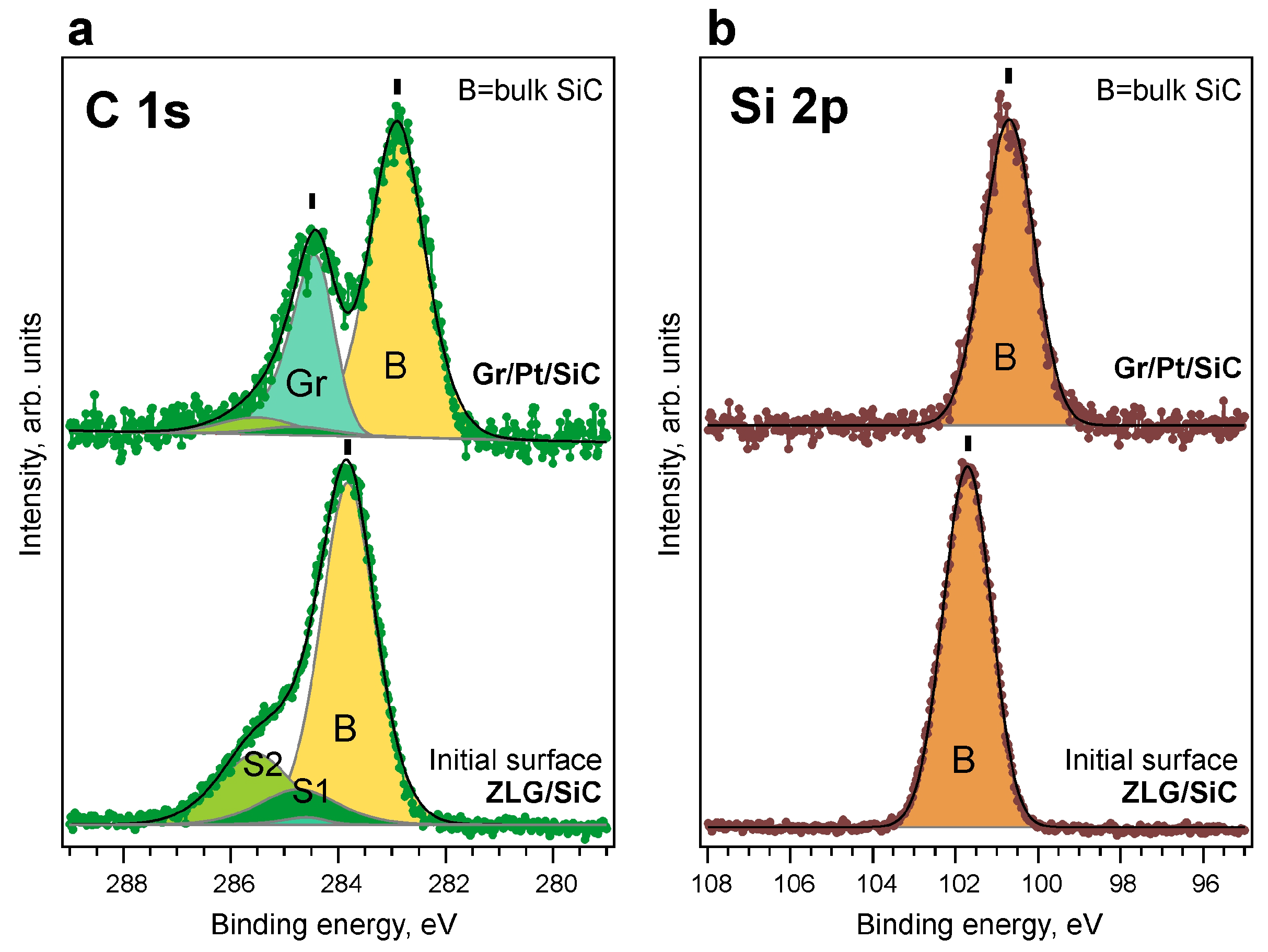
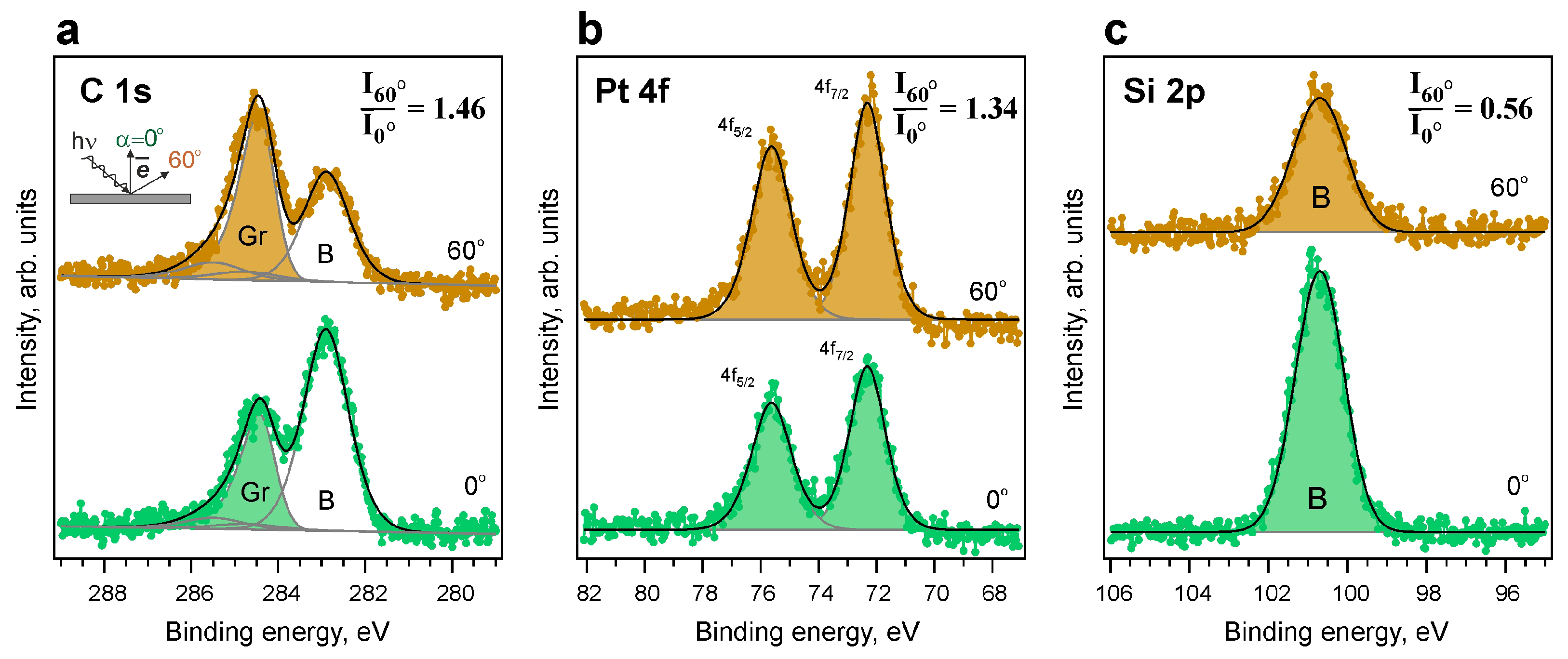
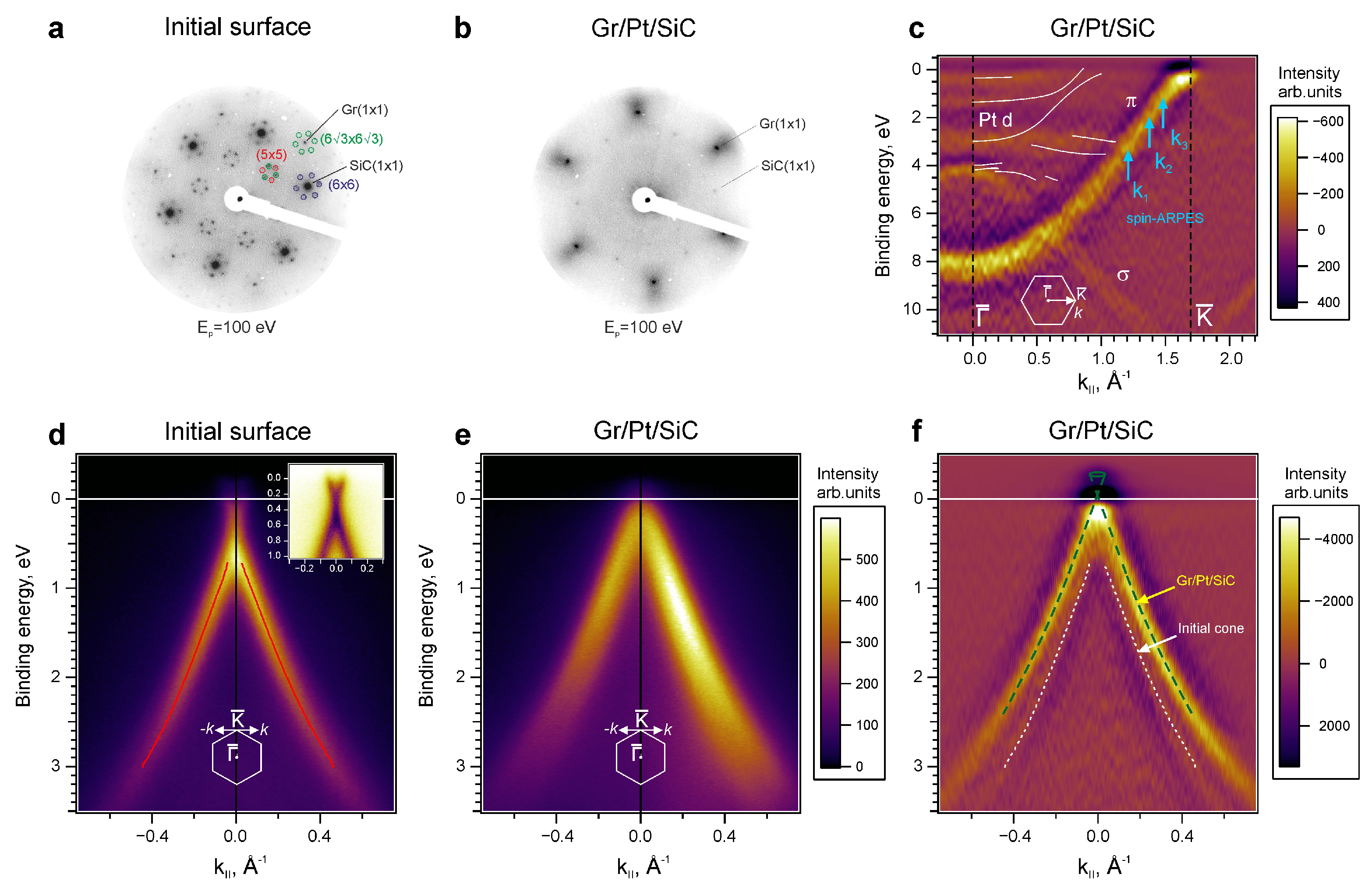
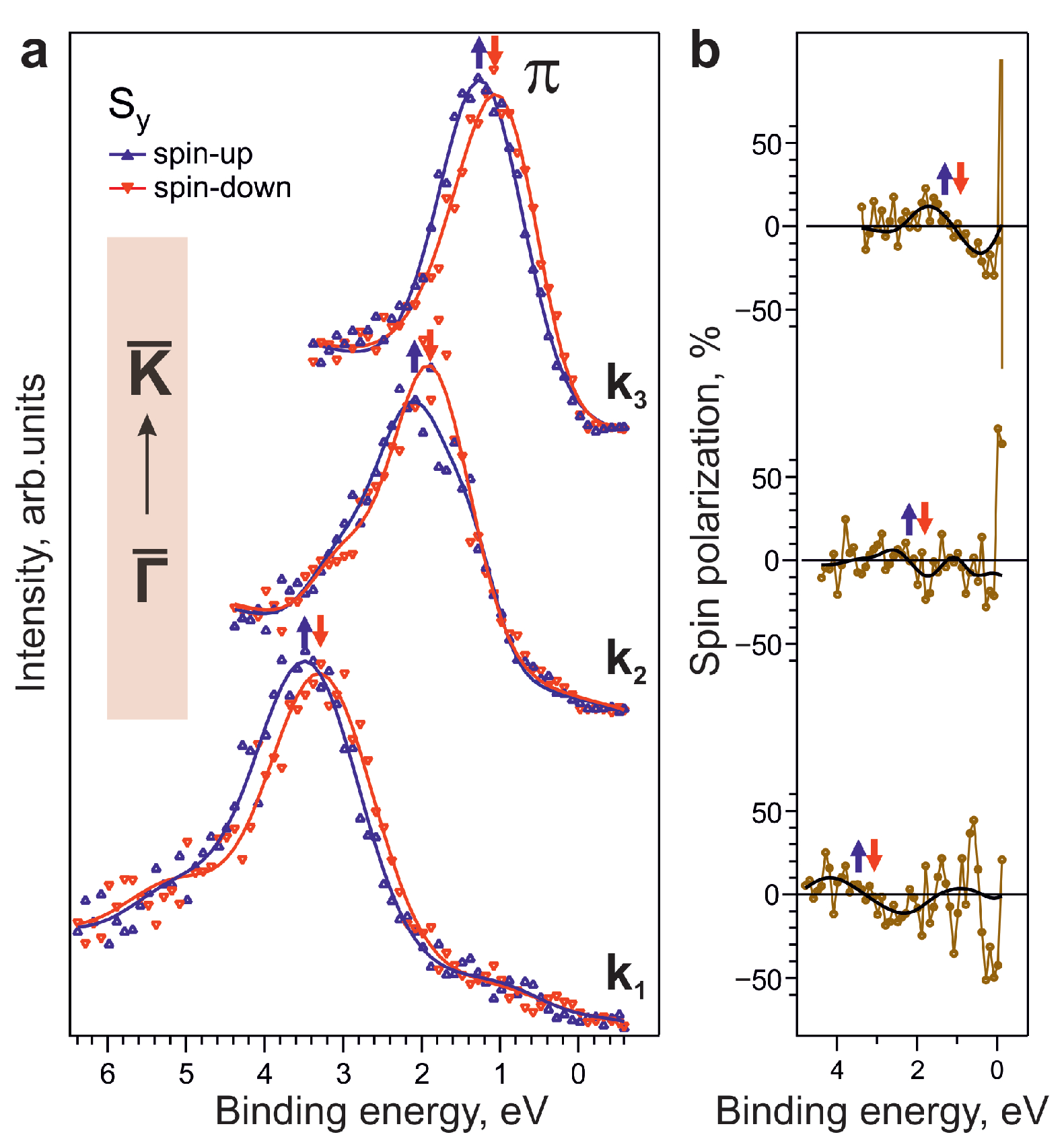
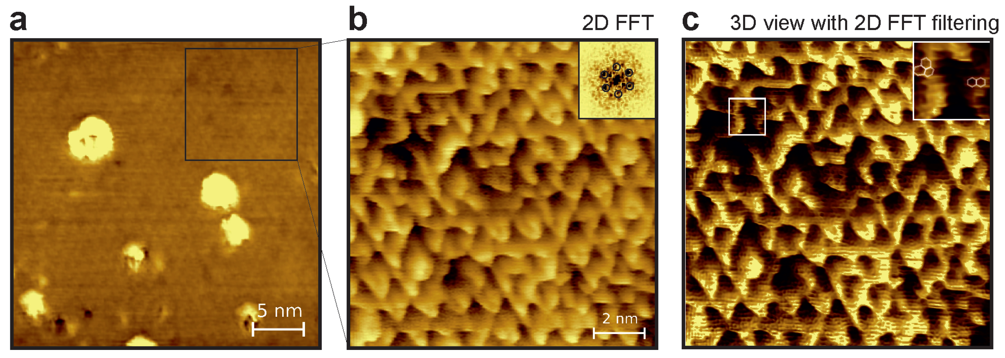
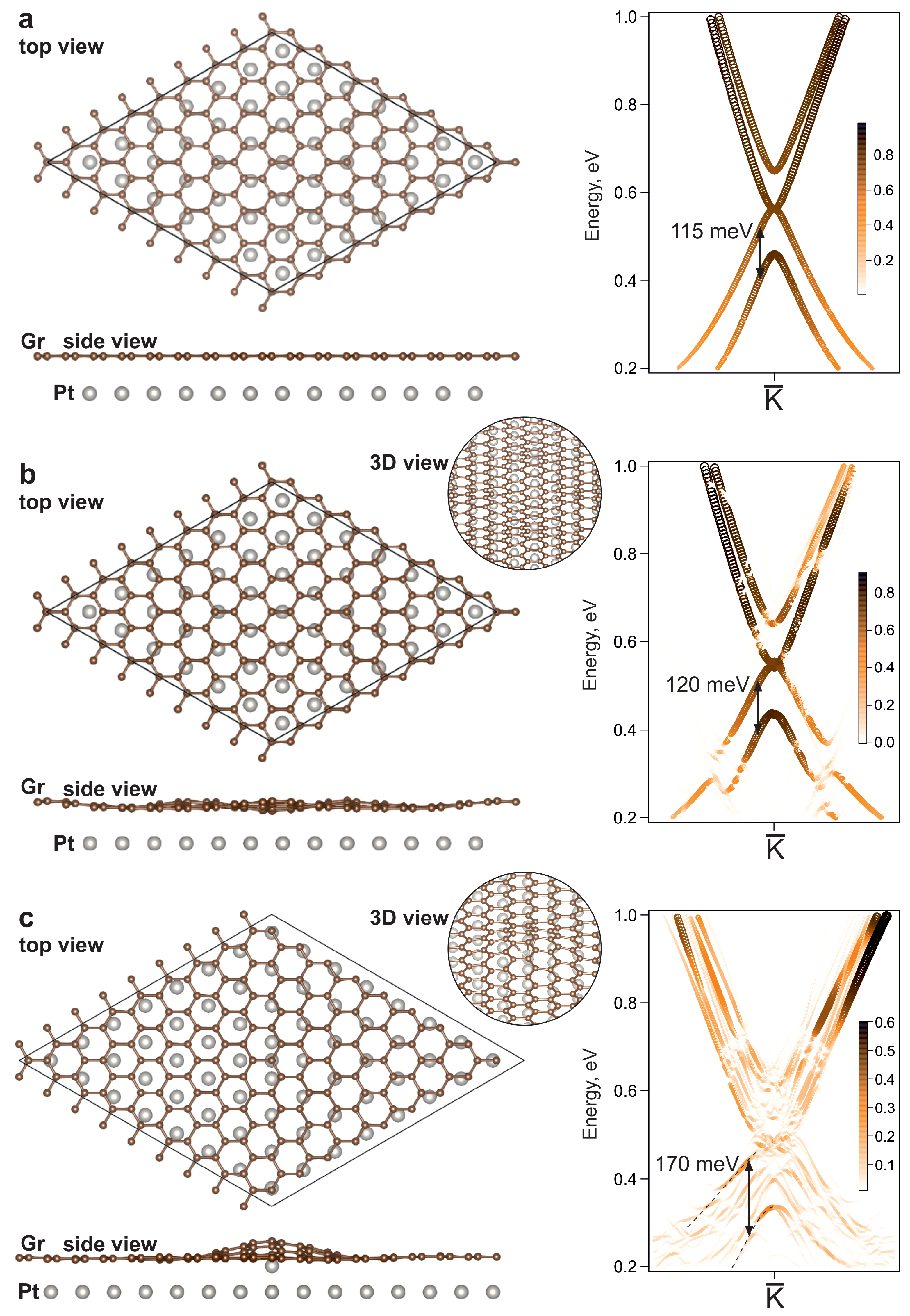
3. Results and Discussion

Initially, zero-layer graphene on SiC(0001) was synthesized at a temperature of about T = 1250 °C. Figure 1 shows the C 1s and Si 2p core levels’ spectra before and after Pt intercalation. Deconvolution of the photoelectron spectra into components by the fitting procedure is presented. The C 1s spectrum of ZLG (Figure 1a) has a characteristic shape with three components: two components, S1 (284.7 eV) and S2 (285.5 eV), corresponding to the carbon in ZLG, and the component of bulk carbon (denoted by (B)) in the SiC compound (283.8 eV). The Si 2p spectrum (Figure 1b) presents one broad peak at the binding energy of 101.7 eV, which is in agreement with the previous results [30,41,42]. However, the Si spin–orbit coupling doublet ( 2 p 1 / 2 and 2 p 3 / 2 ) is not resolved, so one asymmetric peak is obtained during the fitting procedure. It should be noted that a small amount of graphene monolayer accompanies the initial ZLG (see a low-intensity component at 284.6 eV in Figure 1a). However, as shown below, this surface part is inert to the intercalation process.
After Pt deposition and subsequent annealing at T = 1100 °C, we observed the changes in the XPS spectra. Firstly, they are followed by a decrease in the ZLG components and bulk component of carbon atoms in the SiC and an increase in the graphene component at a binding energy of 284.4 eV. That means the transformation of ZLG into a graphene monolayer by an intercalation process. Secondly, the spectral components corresponding to Si and C atoms in the bulk SiC are shifted by 0.9 eV towards lower binding energies. This effect can be explained by different surface band bending in the system due to the Pt atoms’ influence on the interface [43].
To determine the depth position of subsurface layers, we carried out additional measurements of photoelectron spectra at varying emission angles. By studying the angular dependencies of XPS core level intensities of the elements, it is possible to ascertain the relative positions of the layers in depth (see, for example, Supplemental Material of Ref. [44]). In general, a more surface-sensitive spectrum corresponds to a larger photoemission angle. The C 1s, Pt 4f and Si 2p spectra measured at photoemission angles of 0 and 60 relative to the surface normal are presented in Figure 2. When we compare the I 60 / I 0 intensity ratios of the C 1s graphene component, Pt 4f components and Si 2p bulk component (the numerical values of the ratios are shown in the Figure 2), we can conclude that graphene is situated above the Pt submonolayer, with the latter located between the graphene and SiC substrate. This proves that there is a successful intercalation of Pt between ZLG and SiC.
LEED image in Figure 3a shows the formation of ZLG on SiC with ( 6 3 × 6 3 ) and ( 5 × 5 ) reconstructions [45]. The bright reflexes of SiC are clearly observed together with the very pale reflexes of graphene and a set of diffraction spots characteristic of the 6 3 or ZLG reconstruction. It is known that diffraction spots corresponding to the graphene reciprocal lattice slightly increase in intensity upon the forming of the first graphene layer [32]. Indeed, we observe such an increase in the intensity and an appearance of fuzzy diffraction spots of the moiré pattern after Pt intercalation (Figure 3b). Diffraction spots of the ZLG reconstruction are no longer visible, proving the successful intercalation of Pt atoms between ZLG and SiC substrate. The observation of SiC ( 1 × 1 ) diffraction spots up to high kinetic energies (∼200 eV) evidences the good crystal quality of the substrate after intercalation. Notably, the measured period of superstructure ∼(5 × 5) (∼1.2 nm × 1.2 nm) by the STM method perfectly agrees with the predicted one for the 0 rotation angle between the graphene and Pt layer [46].
To analyze the electronic structure of the system, the ARPES intensity maps were measured before and after Pt deposition (Figure 3c–f). Due to the fact that the electronic structure of ZLG does not have intense electronic states near the Fermi level, even a small amount of a graphene layer will contribute to the signal in ARPES spectra. Thus, the initial surface was characterized by the presence of the graphene Dirac cone typical for graphene on SiC with n-doping and the Dirac point energy position at about 0.42 eV below the Fermi level (see Figure 3d) [30]. However, the graphene coverage was much less than the ZLG one according to the XPS data analysis.
After Pt intercalation, a new Dirac cone is clearly visible on the ARPES intensity maps in Figure 3e,f. This cone is related to the intercalated graphene monolayer formed by ZLG transformation. It is shifted above the Fermi level (p-doping) due to Pt intercalation. At the same time, the initial Dirac cone remains unchanged. The band structure in the Γ K ¯ direction is shown in Figure 3c. The dispersions of π and σ graphene states are observed, and Pt d bands are visible near the Fermi level. At the Γ ¯ point, the π state has the binding energy of 8.2 eV, which is consistent with results for graphene on Pt(111) in Ref. [13]. The Pt surface states observed in Refs. [13,20] are shown by white solid lines and coincide with the intense features of the ARPES map. The Pt d bands could be less resolved due to a smaller amount of intercalated Pt relative to the study of the Gr/Pt/Ir(111) system [20] and formation of atomic chains and 2D Pt clusters underneath the graphene. The quantization of Pt bands will be of decisive importance in this case, as was demonstrated in the study of the electronic structure of pentacene molecules on the Ni(110) surface [47].
The spin structure of the intercalated graphene system was measured by the spin-ARPES at k values marked by blue arrows in Figure 3c. The spin-resolved photoemission spectra are shown in Figure 4 for the in-plane Rashba spin component (S y ). The analysis of spin-resolved ARPES data was carried out by a standard procedure (see, for example, the Supplementary Material in Ref. [16]. We start from the calculation of the spin polarization in the following way:
P = 1 S × I L I R I L + I R ,
where I L and I R are the intensities of the scattered photoelectrons collected by the left and right channels of the Mott detector, respectively; S is the Sherman function, equal to 0.14 for the detector at Nanolab setup. The spin polarization is shown in Figure 4b. The slope of the polarization curve and the change in its sign at the energy localization of the π states peak indicate the presence of spin splitting of this peak [48]. Further, the spin-resolved spectra in Figure 4a were obtained using the spin polarization. Spin-up and spin-down intensities were calculated as follows:
I u p = 1 + P 2 × ( I L + I R ) , I d o w n = 1 P 2 × ( I L + I R ) ,
where I u p and I d o w n are up- and down-projections of the spin along defined axis. Calculated data points are shown with the best-fit curves in Figure 4a. Additionally, polarization curves, calculated inversely from the fit data, are illustrated by solid lines in Figure 4b. The fitting procedure for the spin-ARPES data and the spin-splitting estimation are described in the Supplementary Materials. The spin splitting of 200 meV (±50 meV) is observed for all measured spectra in the wide range of the binding energies. Such an experimentally discovered value of spin splitting is unprecedentedly giant for graphene systems, and we will explain this effect.
STM measurements were performed to provide more information about the surface atomic structure. Only one well-ordered structure at large nanometer scales has been resolved, namely the structure of periodic triangular-shaped defects (Figure 5). The periodicity of the superstructure is ∼(5 × 5) relative to the graphene lattice. The 2D fast Fourier transform (2D FFT) image shown on the inset of panel (b) also reveals the superstructure spots. Notably, a topography corrugation of about 0.2–0.3 Å was measured by STM, which is in good agreement with the value reported for graphene on the Pt(111) surface with vacancies in the topmost layer [44,49]. The observation of the corrugation of a comparable magnitude after the intercalation of an incomplete Pt monolayer is evidence that a rarefied platinum layer with holes is formed under graphene. In order to show the presence of a corrugated graphene lattice, we performed a 2D FFT filtering of the image and presented it in a 3D view with illumination. The 2D-FFT image displays six spots corresponding to the superstructure, while the graphene structure is visible in the 3D image (see Figure 5c). In the enlarged image, marked with a white square, a curved graphene lattice is visible due to corrugation. The atomic resolution of graphene deteriorates in some areas caused by simultaneous measurements from different atoms of the corrugated surface, even with a sharp tip showing the atomic resolution of the graphite surface.
To gain insight into the origin of giant Rashba spin–orbit coupling phenomena and make sense of the experimental data obtained, we performed DFT calculations. It is essential to mention that we have been unable to discover any published data on experimental spin–orbit splittings in graphene with energies over 100 meV. Similar experimental splitting values were obtained earlier, but only due to the interplay between the exchange and spin–orbit couplings [16]. Moreover, DFT calculations had significant differences from the experimental results either in the magnitude of the spin–orbit splitting or in the atomic structure of graphene and the underlying layer. Due to the impossibility of taking into account all peculiarities of the real system structure in calculations and the necessity to achieve experimental values of the spin splitting, unrealistic surface models are usually used. In our case of the single-phase system, we can provide the calculations of rather realistic simple model unit cells that might shed some light on the complex origin of the observed giant Rashba phenomenon. By having the single-phase system with a rarefied Pt layer with voids, it is conceivable to theoretically simplify the system as if it consisted of single Pt atoms. The first one is a model of the Gr/Pt interface with flat layers (Figure 6a). The splitting close to 100 meV was obtained at a distance of ∼2.8 Å that is less than the equilibrium distance for the Gr/Pt(111) system (∼3.3–3.4 Å) [44,50]. Nevertheless, even such a close distance is insufficient to obtain a splitting value comparable to the experimental one. It is worth considering that a further reduction in the distance between the graphene and Pt layer leads not only to an increase in the splitting but also to the destruction of the Dirac cone due to strong hybridization with the Pt 5d states. In the second model, we check the influence of graphene corrugation near the average Gr-Pt distance of ∼2.8 Å. The graphene corrugation was obtained after the structure optimization of Gr(8 × 8)/Pt interface with the equilibrium distance of ∼3.3 Å. Since the splitting increased slightly compared to the previous case, even though the carbon atoms now have different distances to the Pt layer, we can conclude that the average distance between the graphene and Pt layer and the number of Pt atoms play a significant role. In order to reduce this average distance without bringing the entire graphene and platinum closer together, we made a point defect in the form of an additional Pt atom under graphene and provided structural optimization of this system. In this case, due to the formation of a “hat-like” structure in graphene above this Pt atom, some of the carbon atoms have a very small distance to the nearest platinum atom (∼2.3 Å), which should increase the spin–orbit coupling induced in graphene. It should also be noted that the structural optimization resulted in the flat areas being even closer to the Pt layer (∼2.5 Å). As it turned out, such a defect enhanced the splitting to ∼170 meV. It is noteworthy that the Dirac dispersion of graphene is not destroyed. Within the experimental resolution, we have a good agreement between this model and the experiment. Thus, essential features revealed for the first time in the calculations are the possibility of graphene corrugation in a large-scale unit cell with a flat substrate and graphene pinning effect in the case of point defects in the form of Pt atoms under graphene.
Without any doubt, the unit cells used in calculations have too small lateral parameters, and a model of the system based on STM data should have a unit cell with minimal dimensions (15 × 15) with a periodic arrangement of voids and a quasi-periodic arrangement of Pt atoms between them. For this reason, our DFT calculations cannot fully take into account the complex structure of the real surface, and a challenging task of large unit cell calculations should be solved to ultimately establish the role of nanometer-scale unit cells in the giant Rashba effect. However, despite the described limitations, we believe that the performed calculations of model unit cells provide a good enough idea of the possible cause of the giant Rashba splitting in the considered system, which consists of a reduction in the average distance between carbon and platinum atoms due to the appearance of an ordered network of platinum clusters and voids under graphene.

4. Conclusions

Our study of Pt-intercalated graphene on SiC substrate revealed ordered single-phase graphene on a rarefied Pt layer with triangular-shaped voids. Corrugated graphene on such a Pt layer has a giant spin-splitting value of about 200 meV. The theoretical model with additional platinum atoms under graphene shows a decrease in the distance between graphene and Pt layer atoms due to the pinning effect and the corrugation of graphene at the sites of point defects. It is supposed that a more complex interface between graphene and the intercalated noble metal layer with pinning defects underlies the giant Rashba effect. Nevertheless, the synthesized system is a good candidate for measuring the spin Hall effect, since it is grown on an undoped silicon carbide substrate, and the intercalation of an incomplete Pt monolayer minimizes the electrical shunting of graphene by metal atoms.

Supplementary Materials

The following supporting information can be downloaded at: https://www.mdpi.com/article/10.3390/sym15112052/s1, Figure S1: ARPES intensity maps and EDC profiles; Figure S2: Spin-resolved ARPES spectra and the spin splittings derived from the fitting procedure.

Author Contributions

Conceptualization, A.A.R. and A.G.R.; methodology, A.A.R., A.A.G., A.V.T., V.Y.V., I.I.K. and A.G.R.; software, A.A.G. and A.V.T.; validation, A.A.R., A.V.T. and A.G.R.; formal analysis, A.A.R., A.A.G., A.V.T., Y.X. and V.Y.V.; investigation, A.A.R., A.A.G., A.V.T., Y.X., V.Y.V., D.A.P., I.I.K., A.E.P., K.A.B. and A.G.R.; resources, A.A.R., A.V.T., D.A.P. and A.E.P.; data curation, A.A.R., A.A.G., A.V.T., Y.X. and A.G.R.; writing—original draft preparation, A.A.R., A.V.T., Y.X., V.Y.V. and A.G.R.; writing—review and editing, all authors; visualization, A.A.R., A.A.G., A.V.T. and A.G.R.; supervision, C.Y., Z.Z. and A.M.S.; project administration, A.G.R.; funding acquisition, A.M.S. All authors have read and agreed to the published version of the manuscript.

Funding

This research was funded by the Ministry of Science and Higher Education of the Russian Federation grant number 075-15-2020-797 (13.1902.21.0024).

Data Availability Statement

The data presented in this study are available on request from the corresponding author, A.A.R.

Acknowledgments

We thank the Resource Center “Physical Methods of Surface Investigation” of Saint Petersburg State University for providing the opportunity to perform the experiment. The calculations were partially performed using the equipment of the Joint Supercomputer Center of the Russian Academy of Sciences (https://rscgroup.ru/en/project/jscc (accessed on 22 November 2022)). The authors thank A.V. Eryzhenkov for providing the possibility of calculations using his band unfolding code.

Conflicts of Interest

The authors declare no conflict of interest.

References

  1. Kane, C.L.; Mele, E.J. Z2 Topological Order and the Quantum Spin Hall Effect. Phys. Rev. Lett. 2005, 95, 146802. [Google Scholar] [CrossRef]
  2. Phong, V.T.; Walet, N.R.; Guinea, F. Effective interactions in a graphene layer induced by the proximity to a ferromagnet. 2D Mater. 2017, 5, 014004. [Google Scholar] [CrossRef]
  3. Eryzhenkov, A.V.; Tarasov, A.V.; Shikin, A.M.; Rybkin, A.G. Non-Trivial Band Topology Criteria for Magneto-Spin-Orbit Graphene. Symmetry 2023, 15, 516. [Google Scholar] [CrossRef]
  4. Chen, L.; Li, F.; Ding, X.M. Rashba spin–orbit coupling induced rectified currents in monolayer graphene with exchange field and sublattice potential. Chin. Phys. B 2023, 32, 087103. [Google Scholar] [CrossRef]
  5. Buša, J.; Pudlák, M.; Nazmitdinov, R. Rippled Graphene as an Ideal Spin Inverter. Symmetry 2023, 15, 1593. [Google Scholar] [CrossRef]
  6. Weeks, C.; Hu, J.; Alicea, J.; Franz, M.; Wu, R. Engineering a Robust Quantum Spin Hall State in Graphene via Adatom Deposition. Phys. Rev. X 2011, 1, 021001. [Google Scholar] [CrossRef]
  7. Shikin, A.M.; Rybkin, A.G.; Marchenko, D.; Rybkina, A.A.; Scholz, M.R.; Rader, O.; Varykhalov, A. Induced spin–orbit splitting in graphene: The role of atomic number of the intercalated metal and pi–d hybridization. New J. Phys. 2013, 15, 013016. [Google Scholar] [CrossRef]
  8. Avsar, A.; Tan, J.Y.; Taychatanapat, T.; Balakrishnan, J.; Koon, G.K.W.; Yeo, Y.; Lahiri, J.; Carvalho, A.; Rodin, A.S.; O’Farrell, E.C.T.; et al. Spin–orbit proximity effect in graphene. Nat. Commun. 2014, 5, 4875. [Google Scholar] [CrossRef]
  9. Brey, L. Spin-orbit coupling in graphene induced by adatoms with outer-shell p orbitals. Phys. Rev. B 2015, 92, 235444. [Google Scholar] [CrossRef]
  10. Ng, S.W.; Noor, N.; Zheng, Z. Graphene-based two-dimensional Janus materials. NPG Asia Mater. 2018, 10, 217–237. [Google Scholar] [CrossRef]
  11. Sino, P.A.L.; Feng, L.Y.; Villaos, R.A.B.; Cruzado, H.N.; Huang, Z.Q.; Hsu, C.H.; Chuang, F.C. Anisotropic Rashba splitting in Pt-based Janus monolayers PtXY (X,Y = S, Se, or Te). Nanoscale Adv. 2021, 3, 6608–6616. [Google Scholar] [CrossRef]
  12. Gong, Q.; Zhang, G. Rashba Splitting and Electronic Valley Characteristics of Janus Sb and Bi Topological Monolayers. Int. J. Mol. Sci. 2022, 23, 7629. [Google Scholar] [CrossRef]
  13. Klimovskikh, I.I.; Tsirkin, S.S.; Rybkin, A.G.; Rybkina, A.A.; Filianina, M.V.; Zhizhin, E.V.; Chulkov, E.V.; Shikin, A.M. Nontrivial spin structure of graphene on Pt(111) at the Fermi level due to spin-dependent hybridization. Phys. Rev. B 2014, 90, 1–10. [Google Scholar] [CrossRef]
  14. Marchenko, D.; Varykhalov, A.; Sánchez-Barriga, J.; Seyller, T.; Rader, O. Rashba splitting of 100 meV in Au-intercalated graphene on SiC. Appl. Phys. Lett. 2016, 108, 172405. [Google Scholar] [CrossRef]
  15. Krivenkov, M.; Golias, E.; Marchenko, D.; Sánchez-Barriga, J.; Bihlmayer, G.; Rader, O.; Varykhalov, A. Nanostructural origin of giant Rashba effect in intercalated graphene. 2D Mater. 2017, 4, 035010. [Google Scholar] [CrossRef]
  16. Rybkin, A.G.; Tarasov, A.V.; Rybkina, A.A.; Usachov, D.Y.; Petukhov, A.E.; Eryzhenkov, A.V.; Pudikov, D.A.; Gogina, A.A.; Klimovskikh, I.I.; Di Santo, G.; et al. Sublattice Ferrimagnetism in Quasifreestanding Graphene. Phys. Rev. Lett. 2022, 129, 226401. [Google Scholar] [CrossRef] [PubMed]
  17. López, A.; Colmenárez, L.; Peralta, M.; Mireles, F.; Medina, E. Proximity-induced spin-orbit effects in graphene on Au. Phys. Rev. B 2019, 99, 085411. [Google Scholar] [CrossRef]
  18. Cano, B.M.; Gudín, A.; Sánchez-Barriga, J.; Clark, O.J.; Anadón, A.; Díez, J.M.; Olleros-Rodríguez, P.; Ajejas, F.; Arnay, I.; Jugovac, M.; et al. Rashba-like spin textures in Graphene promoted by ferromagnet-mediated Electronic-Hybridization with heavy metal. arXiv 2023, arXiv:2206.04351. [Google Scholar]
  19. Guo, G.Y.; Murakami, S.; Chen, T.W.; Nagaosa, N. Intrinsic Spin Hall Effect in Platinum: First-Principles Calculations. Phys. Rev. Lett. 2008, 100, 096401. [Google Scholar] [CrossRef]
  20. Klimovskikh, I.I.; Vilkov, O.; Usachov, D.Y.; Rybkin, A.G.; Tsirkin, S.S.; Filianina, M.V.; Bokai, K.; Chulkov, E.V.; Shikin, A.M. Variation of the character of spin-orbit interaction by Pt intercalation underneath graphene on Ir(111). Phys. Rev. B 2015, 92, 165402. [Google Scholar] [CrossRef]
  21. Briggs, N.; Gebeyehu, Z.M.; Vera, A.; Zhao, T.; Wang, K.; De La Fuente Duran, A.; Bersch, B.; Bowen, T.; Knappenberger, K.L.; Robinson, J.A. Epitaxial graphene/silicon carbide intercalation: A minireview on graphene modulation and unique 2D materials. Nanoscale 2019, 11, 15440–15447. [Google Scholar] [CrossRef]
  22. Xia, C.; Johansson, L.I.; Niu, Y.; Zakharov, A.a.; Janzén, E.; Virojanadara, C. High thermal stability quasi-free-standing bilayer graphene formed on 4H-SiC(0001) via platinum intercalation. Carbon 2014, 79, 631–635. [Google Scholar] [CrossRef]
  23. Premlal, B.; Cranney, M.; Vonau, F.; Aubel, D.; Casterman, D.; De Souza, M.M.; Simon, L. Surface intercalation of gold underneath a graphene monolayer on SiC(0001) studied by scanning tunneling microscopy and spectroscopy. Appl. Phys. Lett. 2009, 94, 1–4. [Google Scholar] [CrossRef]
  24. Yagyu, K.; Tajiri, T.; Kohno, A.; Takahashi, K.; Tochihara, H.; Tomokage, H.; Suzuki, T. Fabrication of a single layer graphene by copper intercalation on a SiC(0001) surface. Appl. Phys. Lett. 2014, 104, 053115. [Google Scholar] [CrossRef]
  25. Sung, S.J.; Yang, J.W.; Lee, P.R.; Kim, J.G.; Ryu, M.T.; Park, H.M.; Lee, G.; Hwang, C.C.; Kim, K.S.; Kim, J.S.; et al. Spin-induced band modifications of graphene through intercalation of magnetic iron atoms. Nanoscale 2014, 6, 3824. [Google Scholar] [CrossRef]
  26. Yang, D.; Xia, Q.; Gao, H.; Dong, S.; Zhao, G.; Zeng, Y.; Ma, F.; Hu, T. Fabrication and mechanism of Pb-intercalated graphene on SiC. Appl. Surf. Sci. 2021, 569, 151012. [Google Scholar] [CrossRef]
  27. Wu, S.; Zhang, Q.; Yang, H.; Ma, Y.; Zhang, T.; Liu, L.; Gao, H.J.; Wang, Y. Advances in two-dimensional heterostructures by mono-element intercalation underneath epitaxial graphene. Prog. Surf. Sci. 2021, 96, 100637. [Google Scholar] [CrossRef]
  28. Gierz, I.; Suzuki, T.; Weitz, R.T.; Lee, D.S.; Krauss, B.; Riedl, C.; Starke, U.; Höchst, H.; Smet, J.H.; Ast, C.R.; et al. Electronic decoupling of an epitaxial graphene monolayer by gold intercalation. Phys. Rev. B 2010, 81, 235408. [Google Scholar] [CrossRef]
  29. Shikin, A.M.; Rybkina, A.A.; Rybkin, A.G.; Klimovskikh, I.I.; Skirdkov, P.N.; Zvezdin, K.A.; Zvezdin, A.K. Spin current formation at the graphene/Pt interface for magnetization manipulation in magnetic nanodots. Appl. Phys. Lett. 2014, 105, 042407. [Google Scholar] [CrossRef]
  30. Riedl, C.; Coletti, C.; Starke, U. Structural and electronic properties of epitaxial graphene on SiC (0 0 0 1): A review of growth, characterization, transfer doping and hydrogen intercalation. J. Phys. D Appl. Phys. 2010, 43, 374009. [Google Scholar] [CrossRef]
  31. Riedl, C.; Coletti, C.; Iwasaki, T.; Zakharov, A.A.; Starke, U. Quasi-free-standing epitaxial graphene on SiC obtained by hydrogen intercalation. Phys. Rev. Lett. 2009, 103, 1–4. [Google Scholar] [CrossRef]
  32. Emtsev, K.V.; Speck, F.; Seyller, T.; Ley, L.; Riley, J.D. Interaction, growth, and ordering of epitaxial graphene on SiC{0001} surfaces: A comparative photoelectron spectroscopy study. Phys. Rev. B Condens. Matter Mater. Phys. 2008, 77, 1–10. [Google Scholar] [CrossRef]
  33. Yazdi, G.R.; Iakimov, T.; Yakimova, R. Epitaxial Graphene on SiC: A Review of Growth and Characterization. Crystals 2016, 6, 53. [Google Scholar] [CrossRef]
  34. Sohn, Y.; Shin, W.; Ryu, S.; Huh, M.; Cha, S.; Kim, K. Graphene p-n junction formed on SiC(0001) by Au intercalation. J. Korean Phys. Soc. 2021, 78, 40. [Google Scholar] [CrossRef]
  35. Jain, V.; Biesinger, M.C.; Linford, M.R. The Gaussian-Lorentzian Sum, Product, and Convolution (Voigt) functions in the context of peak fitting X-ray photoelectron spectroscopy (XPS) narrow scans. Appl. Surf. Sci. 2018, 447, 548–553. [Google Scholar] [CrossRef]
  36. Ozaki, T. Variationally optimized atomic orbitals for large-scale electronic structures. Phys. Rev. B 2003, 67, 155108. [Google Scholar] [CrossRef]
  37. Ozaki, T.; Kino, H. Numerical atomic basis orbitals from H to Kr. Phys. Rev. B 2004, 69, 195113. [Google Scholar] [CrossRef]
  38. Troullier, N.; Martins, J.L. Efficient pseudopotentials for plane-wave calculations. Phys. Rev. B 1991, 43, 1993. [Google Scholar] [CrossRef] [PubMed]
  39. Perdew, J.P.; Wang, Y. Accurate and simple analytic representation of the electron-gas correlation energy. Phys. Rev. B 1992, 45, 13244–13249. [Google Scholar] [CrossRef]
  40. Momma, K.; Izumi, F. VESTA3 Three-Dimens. Vis. Crystal, Vol. Morphol. Data. J. Appl. Crystallogr. 2011, 44, 1272–1276. [Google Scholar] [CrossRef]
  41. Merino, P. Structural Characterization of Epitaxial Graphene. Doctoral Thesis, Universidad Autónoma de Madrid, Madrid, Spain, 2014. [Google Scholar]
  42. Emtsev, K. Electronic and Structural Characterizations of Unreconstructed SiC(0001) Surfaces and the Growth of Graphene Overlayers. Doctoral Thesis, Friedrich-Alexander-Universität Erlangen-Nürnberg, Erlangen, Germany, 2009. [Google Scholar]
  43. Tedesco, J.L.; Rowe, J.E.; Nemanich, R.J. Conducting atomic force microscopy studies of nanoscale cobalt silicide Schottky barriers on Si(111) and Si(100). J. Appl. Phys. 2009, 105, 083721. [Google Scholar] [CrossRef]
  44. Rybkin, A.G.; Rybkina, A.A.; Tarasov, A.V.; Pudikov, D.A.; Klimovskikh, I.I.; Vilkov, O.Y.; Petukhov, A.E.; Usachov, D.Y.; Estyunin, D.A.; Voroshnin, V.Y.; et al. A new approach for synthesis of epitaxial nano-thin Pt5Gd alloy via intercalation underneath a graphene. Appl. Surf. Sci. 2020, 526, 146687. [Google Scholar] [CrossRef]
  45. Riedl, C.; Starke, U.; Bernhardt, J.; Franke, M.; Heinz, K. Structural properties of the graphene-SiC(0001) interface as a key for the preparation of homogeneous large-terrace graphene surfaces. Phys. Rev. B 2007, 76, 245406. [Google Scholar] [CrossRef]
  46. Merino, P.; Svec, M.; Pinardi, A.L.; Otero, G.; Martín-Gago, J.A. Strain-Driven Moiré Superstructures of Epitaxial Graphene on Transition Metal Surfaces. ACS Nano 2011, 5, 5627–5634. [Google Scholar] [CrossRef] [PubMed]
  47. Usachov, D.; Brzhezinskaya, M.; Shikin, A.M.; Adamchuk, V.K. Electronic Structure of Pentacene on Ni(110): Comparison with Graphene. Fuller. Nanotub. Carbon Nanostructures 2010, 18, 487–492. [Google Scholar] [CrossRef]
  48. Meier, F.; Dil, J.H.; Osterwalder, J. Measuring spin polarization vectors in angle-resolved photoemission spectroscopy. New J. Phys. 2009, 11, 125008. [Google Scholar] [CrossRef]
  49. Otero, G.; González, C.; Pinardi, A.L.; Merino, P.; Gardonio, S.; Lizzit, S.; Blanco-Rey, M.; Van de Ruit, K.; Flipse, C.F.J.; Méndez, J.; et al. Ordered Vacancy Network Induced by the Growth of Epitaxial Graphene on Pt(111). Phys. Rev. Lett. 2010, 105, 216102. [Google Scholar] [CrossRef]
  50. Wang, Q.; Pang, R.; Shi, X. Molecular Precursor Induced Surface Reconstruction at Graphene/Pt(111) Interfaces. J. Phys. Chem. C 2015, 119, 22534–22541. [Google Scholar] [CrossRef]
Figure 1. XPS spectra of the C 1s (a) and Si 2p (b) core levels measured for ZLG on SiC—bottom row, and after 1.5 Å Pt intercalation underneath ZLG on SiC—top row. The photon energy is 1486.6 eV.
Symmetry 15 02052 g001
Figure 2. Angle-resolved XPS spectra measured at emission angles of 0 and 60 relative to the surface normal for (a)—C 1s, (b)—Pt 4f and (c)—Si 2p core levels, after Pt intercalation underneath ZLG on SiC. The photon energy is 1486.6 eV.
Symmetry 15 02052 g002
Figure 3. (a,b)—LEED patterns of the initial surface of ( 6 3 × 6 3 ) R30° reconstruction of the SiC surface (zero-layer graphene) with a small amount of graphene monolayer and the surface after 1.5 Å Pt intercalation, E p = 100 eV. (c)—ARPES intensity maps of the surface after Pt intercalation measured along the Γ K ¯ direction of the surface Brillouin zone and presented as the second derivative by energy. (d,e)—ARPES intensity maps of the initial surface and after Pt intercalation measured in the direction orthogonal to the Γ K ¯ . Solid red lines show the result of momentum distribution curves fitting with two Lorentzian peak functions. The enlarged view of the Dirac cone for the initial surface shown in the inset with inverted palette. (f)—ARPES data from (e) presented as the second derivative by energy to discern the main features more clearly. The photon energy is 40.8 eV (He II α ).
Symmetry 15 02052 g003
Figure 4. Spin-ARPES spectra (a) with the spin polarizations (b) of Gr/Pt/SiC(0001) system measured at k 1 , k 2 and k 3 momenta in Figure 3c. In (a), blue and red colors denote opposite sign projections of an electron spin vector, lying in-plane and directed perpendicular to the momentum. The photon energy is 40.8 eV (He II α ).
Symmetry 15 02052 g004
Figure 5. STM images for the system graphene/Pt/SiC after annealing at temperature T = 1100 °C. The image sizes and measurement parameters are as follows: (a) 30 × 30 nm, V s = −0.4 V, I t = 0.5 nA, (b) 11 × 11 nm, V s = −0.5 V, I t = 0.5 nA. A 2D FFT of the STM image is shown on the inset in panel (b). (c) 3D view of the image with 2D FFT filtering for graphene lattice visibility. The enlarged area is presented in the inset.
Symmetry 15 02052 g005
Figure 6. The model slab systems of Gr/Pt interface: (8 × 8) with flat graphene and Pt layer (a), (8 × 8) with a large-scale graphene corrugation (b) and (9 × 9) with graphene corrugation induced by Pt atom (c). The corresponding DFT calculated unfolded bands near K ¯ point along Γ K M ¯ direction of graphene Brillouin zone are shown on the right side. The symbol size and colour palette denote the Bloch spectral weight of carbon atoms for unfolded band structure.
Symmetry 15 02052 g006
Disclaimer/Publisher’s Note: The statements, opinions and data contained in all publications are solely those of the individual author(s) and contributor(s) and not of MDPI and/or the editor(s). MDPI and/or the editor(s) disclaim responsibility for any injury to people or property resulting from any ideas, methods, instructions or products referred to in the content.

