Article

Impact of Carbon Impurities on Air Stability of MOCVD 2D-MoS2

1
Compound Semiconductor Technology, RWTH Aachen University, Sommerfeldstraße 18, 52074 Aachen, Germany
2
Peter-Grünberg-Institute (PGI 7/10) and JARA-FIT, Forschungszentrum Jülich GmbH, 52425 Jülich, Germany
3
Faculty of Georesources and Materials Engineering, RWTH Aachen University, Intzestr. 1, 52072 Aachen, Germany
4
AIXTRON SE, Dornkaulstr. 2, 52134 Herzogenrath, Germany
*
Author to whom correspondence should be addressed.
Surfaces 2023, 6(4), 351-363; https://doi.org/10.3390/surfaces6040025
Submission received: 7 August 2023 / Revised: 20 September 2023 / Accepted: 26 September 2023 / Published: 7 October 2023

Abstract

:
Metal–organic chemical vapor deposition (MOCVD) is a key method for scalable synthesis of two-dimensional transition metal dichalcogenide (2D-TMDC) layers. However, it faces several challenges, such as the unintentional co-deposition of carbon impurities resulting from the pyrolysis of metal–organic precursors. This study investigates the chemical features of carbon and its impact on the photoluminescence property and air stability of 2D-MoS2. Using X-ray photoemission spectroscopy (XPS), it was found that the carbon impurities show characteristics similar to those of sp2-bonded graphitic carbon. Upon prolonged (20–40 weeks) exposure to the atmosphere, the incorporated carbon appears to react with 2D-MoS2, forming a MoS2−xCx solid solution. At the same time, a gradual decrease in the S/Mo ratio implies the formation of sulfur vacancies was also observed. These two processes lead to crystal degradation over time, as evidenced by the gradual quenching of the Raman and photoluminescence (PL) peaks. More detailed PL analyses suggest a charge transfer mechanism between sp2-carbon/2D-MoS2 and 2D-MoS2/air-adsorbates, which, in the short term, could alter PL emissions and appear to further intensify the degradation of 2D-MoS2 in the long-term. The findings highlight the strong impact of unintentionally co-deposited carbon on the optical properties and air stability of MOCVD 2D-MoS2 layers.

Graphical Abstract

1. Introduction

Two-dimensional transition metal dichalcogenides (2D-TMDCs) and their heterostructures have been utilized to demonstrate a variety of electronic and optoelectronic devices such as field-effect transistors (FET) [1], photodetectors [2], memory devices [3], light-emitting diodes (LED) [4], solar cells, sensors [5], etc. However, to transfer all these proof-of-concept devices into commercial applications, many challenges still have to be overcome. Some of them are developing scalable synthesis methods, robust layer transfer processes, as well as device-level issues such as high contact resistance and low carrier mobility [6,7]. Regarding synthesis, a variety of deposition techniques have been explored. These range from molecular beam epitaxy (MBE) [8,9], physical vapor deposition (PVD) [10,11,12], chemical vapor transport (CVT) [13,14], chemical vapor deposition (CVD) [15,16], and metal–organic chemical vapor deposition (MOCVD) [17,18,19,20,21]. MOCVD is known as an established scalable deposition method for compound semiconductors with industrial multi-wafer tools yielding superior homogeneity and reproducibility. However, optimal tool design, synthesis conditions and precursor chemistries [22] of MOCVD processes for TMDCs still have to be developed. In particular, reactive carbon radicals in the reaction chamber originating from the pyrolysis paths of metal–organic precursors [21,23] can lead to unintentional co-deposition of carbon impurities. Carbon co-deposition has also been reported in the CVD of MoS2, originating from impurities present in the MoO3 and S powders used as precursors [24]. The incorporation of carbon into 2D-MoS2 during the MOCVD process, as well as some approaches to avoid it, have been reported [21,25,26,27]. For example, Schaefer et al. have shown that the addition of H2 to the reaction chamber can reduce carbon incorporation into the 2D layer through the etching of the domain edges. The presence of carbon was confirmed by Raman spectroscopy measurement. Carbon-related peaks were found at around 1360 and 1600 cm−1, in analogy to the D and G bands of graphene [28]. A reliable solution to fully mitigate carbon co-deposition is still under investigation. Moreover, in most cases, carbon-related Raman signatures have been the sole criterion for validating the presence of carbon. Lower concentrations may have been overlooked probably due to the relatively low sensitivity of Raman spectroscopy in comparison to other methods such as X-ray photoemission spectroscopy (XPS). Although these works have been dedicated to investigating the co-deposition of carbon during MOCVD, more detailed investigations are yet to be performed to fully comprehend its impact on the properties of 2D-TMDC layers. Vulnerability of 2D-TMDCs, both synthetic (obtained by, e.g., CVD, MOCVD, ALD (atomic layer deposition), etc.) and exfoliated from bulk single crystals against ambient-air exposure, has already been addressed in the literature. However, it was found that synthetic 2D-TMDCs typically possess a higher density of imperfections, such as grain boundaries, edge defects, point defects, impurities etc. [29,30,31]. This does not only degrade electrical properties, e.g., mobility in FET [6], but also turns the material more susceptible to surface reactions with atmosphere and hence to a faster degradation over time. For example, Gao et al. [32] investigated the ambient aging of CVD-MoS2 grown on SiO2/Si. They have shown that severe oxidation occurs at grain boundaries. After one year, MoS2 was found to be significantly degraded, evidenced by scanning electron microscopy (SEM) showing structural changes and cracking. Raman and PL spectra also revealed a serious quenching of intensity over time, a clear indication of a “reduced amount of emitting material”. Peto et al. [33] investigated the oxidation mechanism of 2D-MoS2 obtained from single-crystal exfoliation via scanning tunneling microscopy/spectroscopy (STM/STS). The authors have shown that upon ambient exposure, O atoms tend to be spontaneously incorporated into the basal plane of MoS2. Individual S atoms are replaced with O which is consequently leading to a 2D-MoS2−xOx solid solution. This oxidation process preserves the original crystal lattice with Mo sites in trigonal prismatic configuration. In other works, the role of substrate hydrophobicity [34] and ambient light [35] during the aging of 2D-TMDC layers has been investigated. To the best of our knowledge, the air stability of MOCVD 2D-TMDC layers related to the role of C impurities has not been reported in literature. In this work, we have systematically studied the chemical features of unintentionally co-deposited carbon impurities in MOCVD 2D-MoS2 and their impact on the atmospheric aging behavior and photoluminescence property of these materials.

2. Materials and Methods

Two-dimensional-MoS2 MOCVD. The 2D-MoS2 layers were epitaxially grown in an AIXTRON MOCVD reactor. Sapphire (0001) with a nominal offcut of 0.2o towards m-plane was used as substrate. Prior to deposition, the sapphire was desorbed at 1050 °C in 200 hPa H2 atmosphere for 15 min [36]. Depositions were performed at constant chamber pressure and temperature of 30 hPa and 825 °C, respectively, by H2S-free MOCVD. Di-tert-butyl sulfide (DTBS) and molybdenum hexacarbonyl (Mo(CO)6) were used as sulfur and molybdenum precursors, and N2 as the carrier gas. The molar chalcogen/metal precursor ratio was kept at the constant value of ≈1000 for all depositions. Three different cool-down procedures after the growth step, namely, 2 K min−1 in N2/DTBS (FlowN2: 30,000 sccm; FlowDTBS: 20 µmol/min), ballistic (≈20 K min−1) cool-down in N2 and 2 K min−1 in N2, have been used, which are denoted as 2DTBS, BN2, and 2N2, respectively. Deposition took ≈6 h to obtain a nearly coalesced monolayer (ML) with sparse bilayer (BL) and trilayer (TL) nucleation.
X-Ray Photoemission Spectroscopy (XPS). For XPS measurements, a Versa Probe 5000 tool manufactured by Physical Electronics was used. Monochromatic X-rays are generated by an Al Kα source with an excitation energy of 1486.6 eV. The low-power mode with 25 W with an X-ray spot diameter of about 100 µm was used. To compensate for charging effects, electron neutralization was performed with a neutralizer emission current of 20 µA and a neutralizer bias of 1.37 eV. The Au 4f peak at 84.0 eV was used as the reference to calibrate the binding energy (BE) scale of XPS spectra. Survey scans were performed by 187 eV pass energy. Two high-resolution scans with pass energy set at 10 and 20 eV were performed with step sizes of 0.1 and 0.2 eV, respectively. The latter one was used to carry out quantitative analyses. Regarding the XPS core level analyses, a Shirley function for background subtraction followed by Voigt lineshape deconvolution was used. To characterize the as-deposited 2D layers, they have been stored in an N2 box to minimize atmospheric exposure. The samples were unboxed just before measurement. After the first measurement, the batch of samples was kept in gel boxes and additionally wrapped in Al foil in a clean-room atmosphere to rule out any effect from ambient light over the course of several weeks, during which the measurements were repeated.
Photoluminescence and µ-Raman Spectroscopy. The as-deposited and aged samples were characterized using PL and µ-Raman spectroscopy. Non-resonant Raman and PL spectra were acquired at room temperature using a WiTec confocal Raman microscope equipped with a solid-state 532 nm laser. The laser line was focused on the samples by a 100× microscope objective lens. The collected light was dispersed by 300 grooves/mm and 1800 grooves/mm gratings for PL and µ-Raman measurements, respectively. To prevent laser-induced local heating, the laser power was kept at a low value of 0.7 mW. All PL spectra were fitted using pseudo-Voigt line shapes for A, A0, and B emissions.
Scanning Electron Microscopy (SEM). Morphological characterization of as-deposited and aged samples was performed by scanning electron microscopy (SEM, Zeiss Sigma, Oberkochen, Germany). To quantify the contribution of ML, BL and TL domains as well as the total surface coverage, image processing was performed using the software ImageJ [37].

3. Results and Discussion

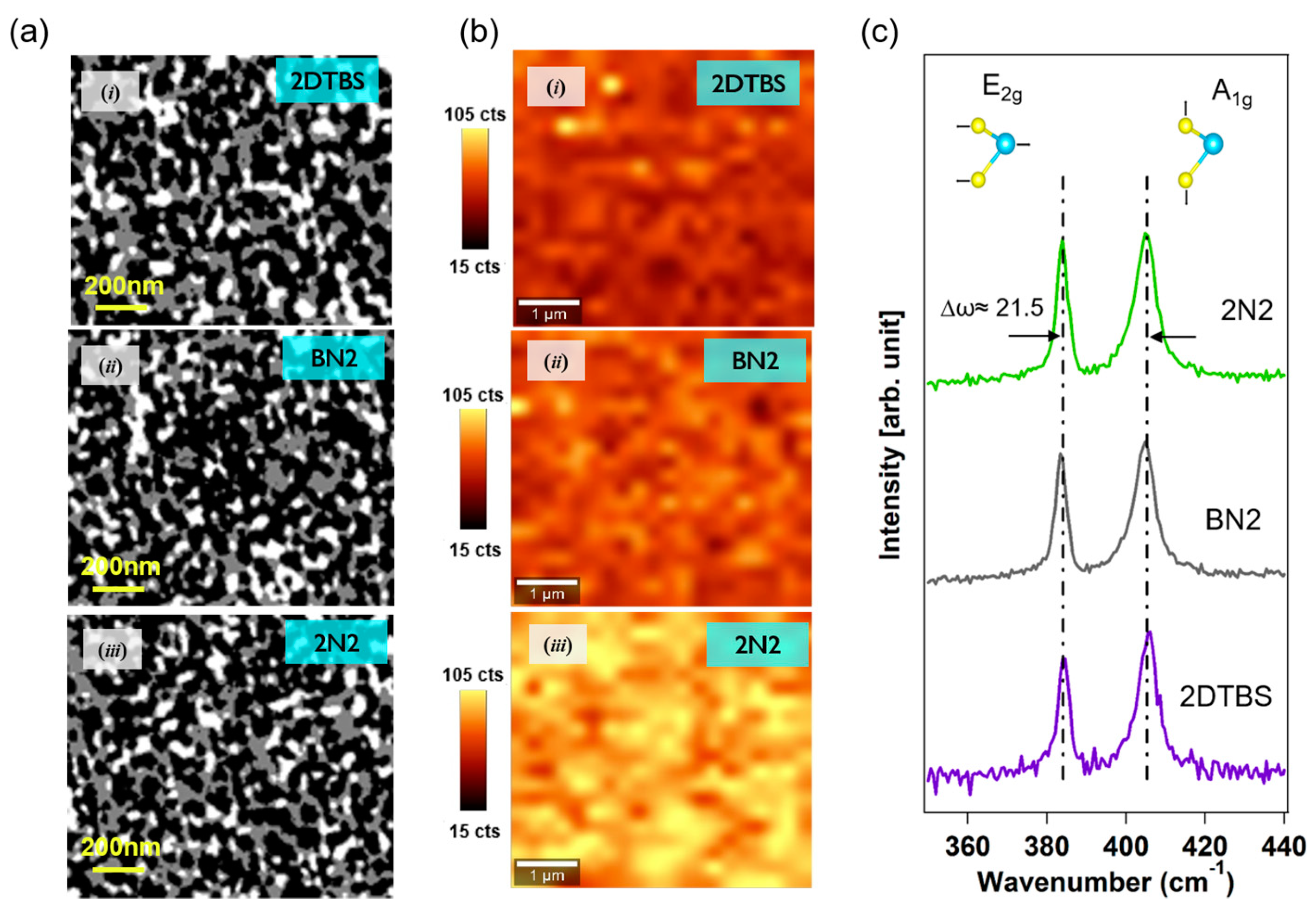
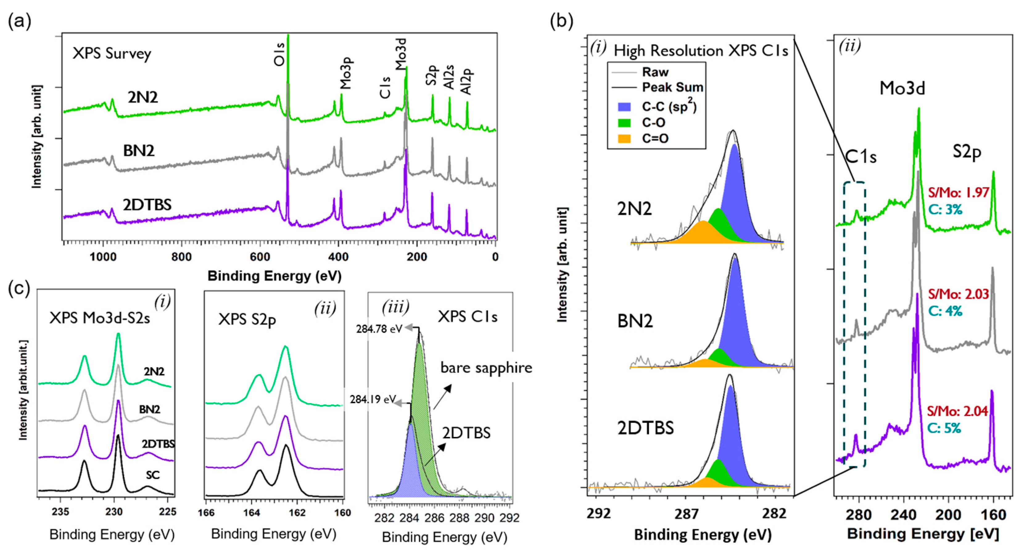
3.1. Characterization of As-Deposited 2D-MoS2 Layers

Segmented SEM pictures of the as-deposited samples are shown in Figure 1a(i)–(iii). Analyses of multiple images using ImageJ reveal similar ML and BL coverage for all 2DTBS, 2N2, and BN2 samples. Values for ML and BL are found to be ≈42% and ≈48%, respectively. All three samples also show a small amount of TL nucleation of about 3% (layer coverages of multiple samples calculated by ImageJ are given in Figure S1a). SEM investigations revealed the uniformity and reproducibility of the 2D layers. We chose three different cool-down conditions in order to produce samples that differ primarily in carbon content while maintaining similar morphology as well as ML and BL coverage. By employing identical growth parameters and only altering the cool-down conditions, we ensure reliable comparisons between samples, which are discerned only by the different co-deposited carbon content.
PL maps of A exciton emission intensity of the as-deposited samples are shown in Figure 1b(i)–(iii). The PL intensity varies considerably between the three different as-deposited samples; 2DTBS and 2N2 show the lowest and highest PL intensity, respectively; this can be linked to the chemical composition of the layers, which will be discussed in more detail later in this section. The corresponding Raman spectra of the samples are also shown in Figure 1c; the characteristic MoS2 Raman peaks, namely, E2g and A1g, are located at ≈383.8 and ≈405.3 cm−1, respectively. These are the first-order Raman modes associated with in-plane and out-of-plane vibrations, respectively [38]. The distance between the two peaks is found to be 21.5 cm−1 and confirms that the surface coverage is dominated by ML and BL contributions in agreement with the SEM analyses [39].
XPS analyses of the as-deposited samples (before exposure to the atmosphere) are given in Figure 2. Since the C1s peak is not dominated by adventitious carbon, the peaks were calibrated with respect to the Al2p peak, explained in detail in the supporting information. The survey scans shown in Figure 2a are dominated by Mo3d, S2p, Al2p, Al2s, C1s and O1s. Mo, S, and C can be ascribed to the MOCVD process. Al and O are attributed to the Al2O3 substrate. Due to the desorption step prior to deposition (see Section 2), negligible carbon contamination on the sapphire is. It should be noted that the substrate signals are detectable because of the ultra-low thickness of the 2D-MoS2, which is 1–3 ML (≈0.72–2.16 nm) [40].
The Mo3d-S2s and S2p core levels are shown in Figure 2c(i) and (ii), respectively. The corresponding curves obtained from a reference MoS2 bulk single crystal (HQ-Graphene, purity > 99.995%), denoted as SC, are also shown for comparison. The binding energy difference between Mo3d5/2 and S2p3/2 (∆BEMo3d-S2p) is found to be 67.1 eV in the single-crystal MoS2, which is in agreement with the literature [41,42]. The corresponding values of ∆BEMo3d-S2p for 2DTBS, 2N2, and BN2 samples are extracted as 67.1, 67.2, and 67.2 eV, respectively. Considering the binding energy difference in addition to the absolute binding energy values makes XPS analyses more reliable because the absolute values can be shifted as a result of, e.g., doping [41], impurities [21], and charging [43]. The core levels verify the formation of pure MoS2 with neither oxide nor carbide components being detected.
The zoomed-in survey spectra, including the Mo3d, S2p, and C1s core levels, along with the S/Mo stoichiometry ratio and the carbon concentration in atomic%, are given in Figure 2b(ii). The stoichiometries were determined by evaluating the ratio between the S2p and Mo3d peak areas and then were normalized to the stoichiometry of the reference single-crystal MoS2 [41,44] assumed to have an S/Mo ratio of 2.0. The carbon atomic percentage obtained from the quantitative analysis represents the contribution of the C-C bond shown in blue in Figure 2b(i). The XPS analysis data and the PL intensity of as-deposited samples are summarized in Table 1.
The S/Mo stoichiometry ratios for all three samples deviate slightly relative from the ideal value of 2.0, indicating the deposition of sulfur-rich or sulfur-deficient 2D-MoS2 layers in comparison to the exfoliated single-crystal counterpart [30,45,46,47]. It is noteworthy that the excess sulfur in the 2DTBS and BN2 samples with an S/Mo ratio higher than 2.0 suggests that some sulfur atoms are present in a different chemical environment other than the Mo-S bond [10]. However, the concentration of these species is not high enough to be distinguished in the S2p core levels (see Figure S2a).
To analyze the carbon species found in our layers in more detail, the high-resolution XPS spectra of the C1s core levels were deconvoluted. The fitted spectra constitute C-C, C-O, and C=O bonds, with the C-C bond dominating the spectra (Figure 2b(i)). It was found that the full width at half-maximum (FWHM) values of the C-C-bond-related peak (blue in Figure 2b(i)) are 1.02 eV, 1.10 eV and 1.08 eV for 2DTBS, 2N2 and BN2, respectively. In comparison, the FWHM values of the carbon peak measured on single-crystal MoS2 and bare sapphire (Figure S2b(ii),(iii)), which originate only from adventitious carbon, were found to be 1.49 eV and 1.48 eV, respectively, showing ≈40% increase relative to the C1s peak (C-C bond) of as-deposited samples. The sharper C1s peak in the MOCVD 2D-MoS2 samples is an indication of a more structured carbon species in these 2D layers.
Moreover, the C1s lineshape shows a broader asymmetric tail toward higher binding energies, which is typical for graphite and graphene [48,49,50,51,52,53]. On the other hand, the binding energy difference between the dominant C1s peak (C-C bond) and Al2p (∆BEC1s-Al2p) on bare sapphire (Figure S2b(i),(ii)) is found to be 209.8 eV; yet ∆BEC1s-Al2p for 2DTBS, 2N2 and BN2 is measured to be 209.2, 209.2 and 209.3 eV, respectively. The systematic shift of the C1s peak towards lower values by ≈0.6 eV in the MOCVD samples moves it close to the typical BE position for the sp2-hybridized C bond in graphene and graphite [48,50,51,54,55,56]. As an example, the C1s core level of sapphire stored in the atmosphere and that of the as-deposited 2DTBS sample are shown in Figure 2c(iii); the C-C bond in the 2DTBS sample features a narrower peak located at lower BE relative to the C-C bond in bare sapphire. Thus, it can be concluded that the carbon species incorporated into 2D-MoS2 layers during MOCVD tend to show more graphitic characteristics than those of adventitious carbon. It is worth mentioning that the wide-range Raman spectra of the samples do not show the carbon-related peaks expected at ≈1360 and ≈1600 cm−1. (Figure S3)
The variation of PL intensities in the as-deposited samples shown as A exciton PL maps in Figure 1b(i)–(iii) can be attributed to the concentration of sp2-C impurities in these samples. The A exciton peak consists of the neutral A0 exciton and the negatively charged A trion with emissions at around 1.89 eV and 1.86 eV, respectively [21,57]. A0 usually dominates the spectra because of reduced non-radiative recombination probability [58]. A appears when MoS2 has a significant electron concentration in the conduction band (n-type characteristic), which can be induced by, e.g., sulfur vacancies, chemical doping [59], [60], or strain [61,62]. It can be seen that the PL intensity is clearly reduced by the increase in the sp2-C concentration (see Table 1). Accordingly, samples 2DTBS and 2N2 with five and three atomic% carbon feature the lowest and highest intensity, respectively. It has already been reported that 2D-MoS2 PL attenuation occurs in the presence of carbon, e.g., if MoS2 forms a heterostructure with graphene quantum dots (GQD) or graphene [57,63]. This observation is attributed to the transfer of electrons from GQD/graphene to MoS2, which leads to an attenuation in A0 exciton emissions [63,64,65].

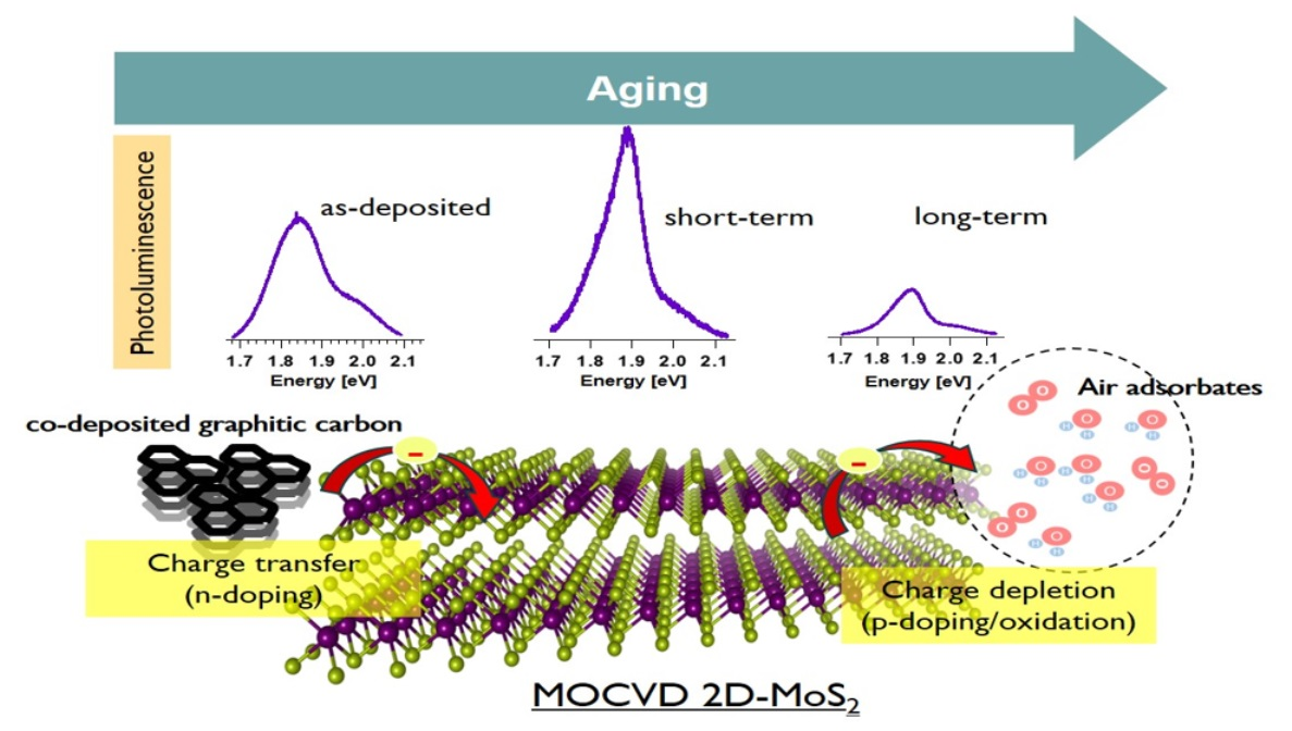
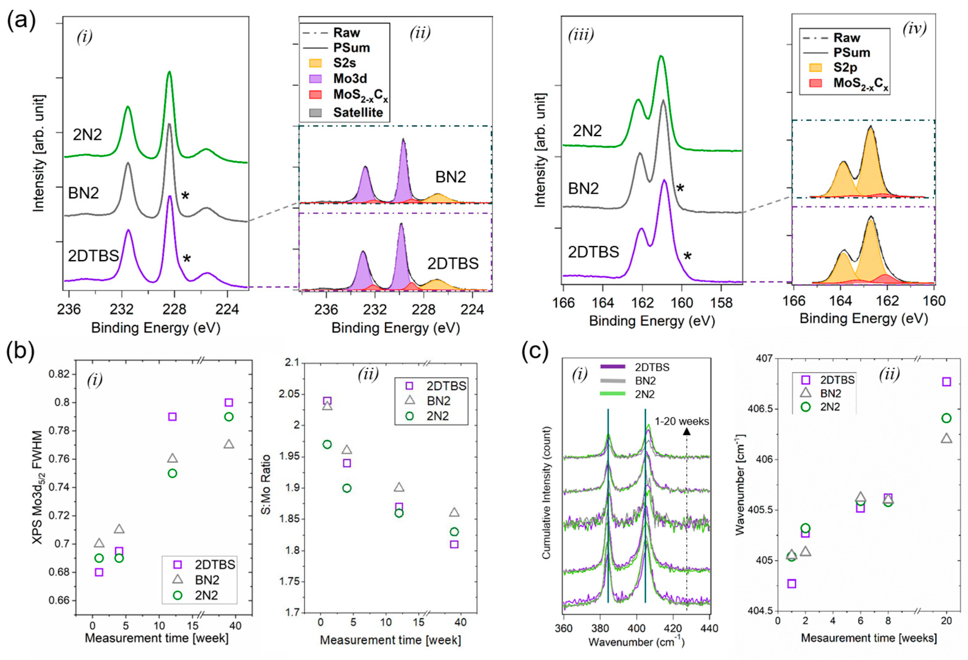
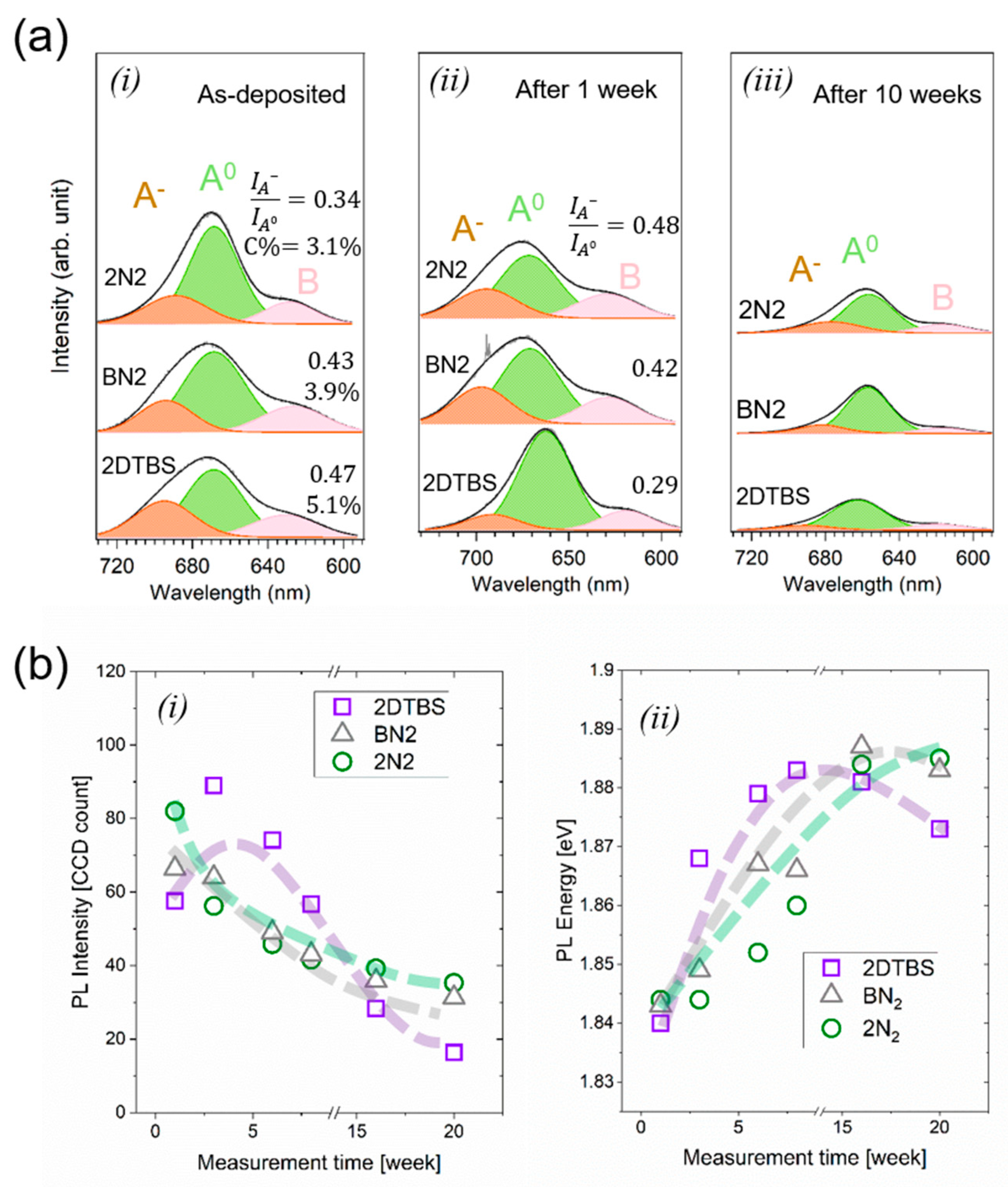
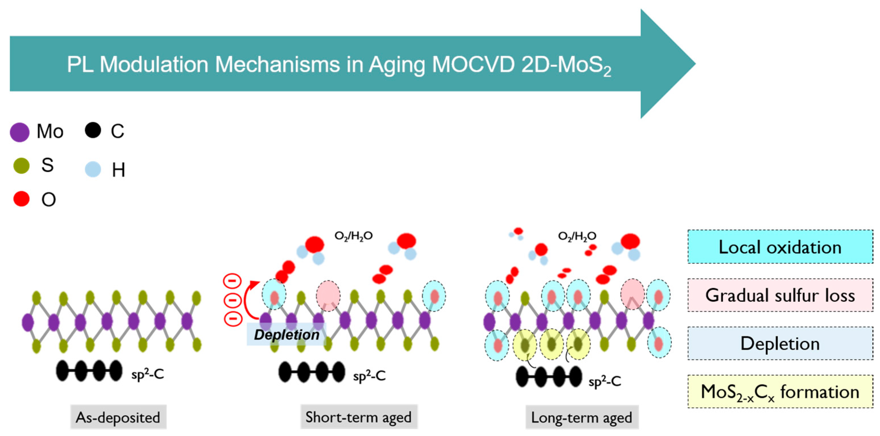
3.2. Aging of MOCVD 2D-MoS2

All samples were exposed to ambient air for 40 weeks, with several XPS measurements performed during this time span. The FWHM values of XPS Mo3d5/2 and S2p3/2 given in Figure 3b(i) show a gradual increase, which is an indication of the reduced crystal quality of the 2D-MoS2 layers. This could be due to various factors, such as accumulation of structural defects, impurities, oxidation, etc.
Moreover, desulfurization has also been evidenced by XPS analysis; the S:Mo stoichiometry ratio measured over the 40-week period shows a gradual decrease (Figure 3b(ii)). The highest degree of sulfur loss is detected for the 2DTBS sample, with ≈8%.
XPS Mo3d and S2p core levels of the 40-week-aged samples (Figure 3a(i) and (iii)) do not indicate any oxidation after 40 weeks. Oxidation would be identified by additional shoulders located towards higher binding energies relative to the Mo3d5/2 and Mo3d3/2 peaks of MoS2 caused by Mo-O bonds. Possibly, these features lie below the sensitivity limit of the XPS tool, which is a ≈1 atomic % concentration. However, in some other works utilizing XPS measurements, the formation of significant densities of transition metal oxides after a few weeks was reported [32,66]. The fact that the concentration of oxide species did not reach the XPS detection limit after 40 weeks might be attributed to the higher stability of the 2D layers investigated in this work. Such higher stability could be due to the (nearly) coalesced morphology of the layers and the fact that the stability is especially dependent on the density of defects (including edge defects) in the pristine material [33,67].
It should be noted that the number of oxide compounds or O2/H2O on the surface/edges of 2D-MoS2 layers may not reach the XPS-detectable level (which is ≈1 atomic%), although physiosorbed or chemisorbed O2/H2O species are likely present. Previous studies, such as the work by Peto et al. [33], utilizing a more sensitive method (STM/STS), have demonstrated the formation of atomic level solid-solution-type 2D-MoS2−xOx formed during ambient exposure of single-crystal MoS2 while XPS failed to detect any covalent oxygen bonding to the top sulfur atoms or the formation of oxidized MoO3 areas. Additionally, the presence of adsorbed O2/H2O on 2D-MoS2 can be confirmed by Raman and PL spectroscopy.
Moreover, the XPS core levels show a minor yet clearly detectable amount of carbide species after 40 weeks of ambient exposure for the 2DTBS and BN2 samples. These species appeared as a shoulder peak towards lower binding energies of both Mo3d and S2p core levels (marked by the asterisk symbol in Figure 3a(i),(iii)). Deconvoluted high-resolution XPS spectra of the Mo3d, S2p (Figure 3a(ii),(iv)), and C1s (Figure S2c) core levels of samples 2DTBS and BN2 revealed that the newly emerged shoulder peak can be attributed to MoS2−xCx. The emerged carbide peaks are located at binding energies which are 0.85, 0.65, and 0.86 eV lower than those of Mo3d5/2, S2p3/2, and C1s (C-C bond) peaks, respectively, which is in good agreement with the values reported in the literature [68,69]. The formation of MoS2−xCx suggests that sp2-C tends to react with MoS2 over time. The atomic concentrations of MoS2−xCx species detected in samples 2DTBS and BN2 were found to be ≈12% and ≈7%, respectively. The XPS O1s peak, as well as the SEM morphology of aged layers, are given in Figure S3.
The formation of carbide species upon exposure of 2D-TMDC layers to ambient is potentially exclusive to the MOCVD layers, in which sp2-carbon impurities are co-deposited due to the use of metal–organic precursors in this method.
Raman spectra of the samples exposed to the atmosphere measured at different time intervals are shown in Figure 3c(i); the intensity of the characteristic E2g and A1g peaks for all three samples show a gradual decrease over time, which is an indication of layer degradation. Moreover, the A1g peak exhibits a gradual shift toward higher frequencies (Figure 3c(ii)); this can be attributed to the adsorption of air molecules on the surface, which restrain the out-of-plane vibrational mode and introduce compressive strain along the c direction of the unit cell [70].
The fitted PL spectra for the as-deposited samples after one week and after ten weeks of exposure to the atmosphere are given in Figure 4a. As explained before, in the as-deposited samples, the intensity of the trion peak A and, accordingly, the I A I A 0 ratio increases with a rising sp2-C concentration.
Interestingly, in the one-week-aged samples, unlike their as-deposited counterparts, it was observed that the I A I A 0 ratio is inversely correlated to sp2-C concentration. This observation can be attributed to the interaction of the 2D-MoS2 film with the ambient atmosphere. The accumulation of negative charge in the 2D-MoS2 transferred from the sp2-C (as described before) makes the adsorption of O2/H2O to the 2D-MoS2 energetically more favorable [34]. The enhanced adsorption results from a probably reduced work function (WF) of 2D-MoS2 due to the charge transfer n-doping by sp2-C [71]. Following that, adsorbed H2O/O2 molecules deplete the negative charges, leading to a reduced A recombination and enhanced A0 exciton emissions.
The PL of 10-week-aged samples (Figure 4a(iii)) shows a significant quenching for all three samples, which is an indication of degraded layers and the reduction in emitting materials regardless of the concentration of sp2-C.
The PL intensity of the A exciton and its energy position over the course of 20 weeks of ambient exposure is presented in Figure 4b(i) and (ii), respectively. Exciton emission energies show a gradual blue shift over a period of ≈15 weeks. After that, especially for the 2DTBS sample (with the highest carbon content), a slight red-shift occurs. The PL emission blue-shift is consistent with the presence of H2O/O2 adsorbates at the surface and the consequent p-doping of MoS2 layers [72] and confirms the trend of the gradual blue-shift of the Raman A1g vibrational mode discussed previously. The consecutive red shift might be attributed to the general degradation mechanisms of MoS2 exposed to the atmosphere.
The atmospheric aging of MOCVD 2D-MoS2 involves multiple factors that can either enhance or quench the PL emission. For example, the adsorption of O2/H2O air molecules can lead to the p-doping of MoS2, resulting in an increase in PL emissions [73,74]. Conversely, the aging process can also introduce various defects, acting as non-radiative recombination centers. Depending on the dominant factor at different stages of aging, the PL emissions can either be enhanced or exhibit a drop in intensity. An illustrative example is observed in the 2DTBS sample, which has the highest sp2-C content. During the early stages of aging, this sample shows an enhancement in the PL emission, suggesting the dominant effect of p-doping; however, after 20 weeks, a more pronounced quenching of the PL is observed in comparison to the other samples. This quenching can be attributed to the increased formation of structural defects, as supported by XPS analysis revealing the presence of carbide species. The dominant mechanisms defining PL emissions during atmospheric aging of MOCVD 2D-MoS2 are schematically presented in Figure 5.

4. Conclusions

In summary, we have investigated the photoluminescence property and air stability of nearly coalesced MOCVD 2D-MoS2 layers, considering the role of unintentionally co-deposited carbon impurities. The characteristics and impact of incorporated carbon have been studied using XPS and PL characterization and revealed its graphitic sp2-C character. Carbon impacts the photoluminescence properties of 2D-MoS2 by effective n-type doping, facilitating a charge transfer between 2D-MoS2 and atmospheric adsorbates after exposure to air. It is especially notable that these effects are observed for C concentrations lying below the detection limit of Raman spectroscopy. O2/H2O adsorption was evidenced by PL and Raman A1g vibrational mode blue shifts. On a timescale of 20–40 weeks, sp2-C tends to react with 2D-MoS2 and forms MoS2−xCx. However, the precise location of impurities and adsorbates, as well as the exact chemical reactions, are not known and yet to be more thoroughly investigated, e.g., by more sensitive experimental methods (e.g., STM/STS). Moreover, it was found that even after 40 weeks of exposure, the 2D layers studied in this work did not show any oxidation detectable by XPS measurement. However, both PL and Raman spectroscopy of the aged layers indicated a clear drop in intensity, regardless of their initial carbon concentration, which is an indication of crystal degradation.

Supplementary Materials

The following supporting information can be downloaded at: https://www.mdpi.com/article/10.3390/surfaces6040025/s1, Figure S1: extended SEM analyses of as-deposited layers; Figure S2: fitted high-resolution of (a) Mo3d-S2s and S2p core levels of as-deposited samples, (b) Al2p and C1s core levels of bare sapphire and C1s core level of single crystal MoS2; (c) C1s core levels of 40-week-aged 2DBS and BN2 samples; Figure S3: XPS O1s spectra of as-deposited, 20-week- and 40-week-aged samples, as well as SEM of 40-week-aged layers. Figure S4: extended µ-Raman spectra of as-deposited samples and Figure S5: distribution of A0 PL intensity, obtained from the PL maps given in Figure 1 [21,23,32,34,36,75,76,77].

Author Contributions

Conceptualization, A.G. (Amir Ghiami); methodology, A.G. (Amir Ghiami), A.G. (Annika Grundmann); validation, A.G. (Amir Ghiami), A.V. and H.K.; formal analysis, A.G. (Amir Ghiami); investigation, A.G. (Amir Ghiami), H.F., S.T., S.A. and Z.W.; resources, A.V., S.H.-E. and M.H.; writing—original draft preparation, A.G. (Amir Ghiami); writing—review and editing, A.V. and H.K.; visualization, A.G. (Amir Ghiami); supervision, A.V. All authors have read and agreed to the published version of the manuscript.

Funding

This work has been financially supported by Federal Ministry of Education and Research (BMBF), NEUROTEC project; project no. 16ME0398K and 16ME0399, Germany.

Institutional Review Board Statement

Not applicable.

Informed Consent Statement

Not applicable.

Data Availability Statement

The presented in this study are available in the article and Supplementary Materials.

Conflicts of Interest

The authors declare no conflict of interest.

References

  1. Radisavljevic, B.; Radenovic, A.; Brivio, J.; Giacometti, V.; Kis, A. Single-Layer MoS2 Transistors. Nat. Nanotechnol. 2011, 6, 147–150. [Google Scholar] [CrossRef] [PubMed]
  2. Lim, Y.R.; Song, W.; Han, J.K.; Lee, Y.B.; Kim, S.J.; Myung, S.; Lee, S.S.; An, K.S.; Choi, C.J.; Lim, J. Wafer-Scale, Homogeneous MoS2 Layers on Plastic Substrates for Flexible Visible-Light Photodetectors. Adv. Mater. 2016, 28, 5025–5030. [Google Scholar] [CrossRef] [PubMed]
  3. Cao, G.; Meng, P.; Chen, J.; Liu, H.; Bian, R.; Zhu, C.; Liu, F.; Liu, Z. 2D Material Based Synaptic Devices for Neuromorphic Computing. Adv. Funct. Mater. 2020, 31, 2005443. [Google Scholar] [CrossRef]
  4. Andrzejewski, D.; Oliver, R.; Beckmann, Y.; Grundmann, A.; Heuken, M.; Kalisch, H.; Vescan, A.; Kümmell, T.; Bacher, G. Flexible Large-Area Light-Emitting Devices Based on WS2 Monolayers. Adv. Opt. Mater. 2020, 8, 2000694. [Google Scholar] [CrossRef]
  5. Jiao, K.; Duan, C.; Wu, X.; Chen, J.; Wang, Y.; Chen, Y. The Role of MoS2 as an Interfacial Layer in Graphene/Silicon Solar Cells. Phys. Chem. Chem. Phys. 2015, 17, 8182–8186. [Google Scholar] [CrossRef]
  6. Rai, A.; Movva, H.C.P.; Roy, A.; Taneja, D.; Chowdhury, S.; Banerjee, S.K. Progress in Contact, Doping and Mobility Engineering of MoS2: An Atomically Thin 2D Semiconductor. Crystals 2018, 8, 316. [Google Scholar] [CrossRef]
  7. Schranghamer, T.F.; Sharma, M.; Singh, R.; Das, S. Review and Comparison of Layer Transfer Methods for Two-Dimensional Materials for Emerging Applications. Chem. Soc. Rev. 2021, 50, 11032–11054. [Google Scholar] [CrossRef] [PubMed]
  8. Roy, A.; Movva, H.C.P.; Satpati, B.; Kim, K.; Dey, R.; Rai, A.; Pramanik, T.; Guchhait, S.; Tutuc, E.; Banerjee, S.K. Structural and Electrical Properties of MoTe2 and MoSe2 Grown by Molecular Beam Epitaxy. ACS Appl. Mater. Interfaces 2016, 8, 7396–7402. [Google Scholar] [CrossRef]
  9. Mortelmans, W.; El Kazzi, S.; Groven, B.; Nalin Mehta, A.; Balaji, Y.; De Gendt, S.; Heyns, M.; Merckling, C. Epitaxial Registry and Crystallinity of MoS2 via Molecular Beam and Metalorganic Vapor Phase van Der Waals Epitaxy. Appl. Phys. Lett. 2020, 117, 033101. [Google Scholar] [CrossRef]
  10. Timpel, M.; Ligorio, G.; Ghiami, A.; Gavioli, L.; Cavaliere, E.; Chiappini, A.; Rossi, F.; Pasquali, L.; Gärisch, F.; List-Kratochvil, E.J.W.; et al. 2D-MoS2 Goes 3D: Transferring Optoelectronic Properties of 2D MoS2 to a Large-Area Thin Film. npj 2D Mater. Appl. 2021, 5, 64. [Google Scholar] [CrossRef]
  11. Ghiami, A.; Timpel, M.; Chiappini, A.; Nardi, M.V.; Verucchi, R. Synthesis of MoS2 Thin Film by Ionized Jet Deposition: Role of Substrate and Working Parameters. Surfaces 2020, 3, 683–693. [Google Scholar] [CrossRef]
  12. Serna, M.I.; Yoo, S.H.; Moreno, S.; Xi, Y.; Oviedo, J.P.; Choi, H.; Alshareef, H.N.; Kim, M.J.; Minary-Jolandan, M.; Quevedo-Lopez, M.A. Large-Area Deposition of MoS2 by Pulsed Laser Deposition with in Situ Thickness Control. ACS Nano 2016, 10, 6054–6061. [Google Scholar] [CrossRef] [PubMed]
  13. Zhou, H.; Wang, C.; Shaw, J.C.; Cheng, R.; Chen, Y.; Huang, X.; Liu, Y.; Weiss, N.O.; Lin, Z.; Huang, Y.; et al. Large Area Growth and Electrical Properties of P-Type WSe2 Atomic Layers. Nano Lett. 2015, 15, 709–713. [Google Scholar] [CrossRef]
  14. Huang, J.; Yang, L.; Liu, D.; Chen, J.; Fu, Q.; Xiong, Y.; Lin, F.; Xiang, B. Large-Area Synthesis of Monolayer WSe2 on a SiO2/Si Substrate and Its Device Applications. Nanoscale 2015, 7, 4193–4198. [Google Scholar] [CrossRef]
  15. Kim, H.; Ovchinnikov, D.; Deiana, D.; Unuchek, D.; Kis, A. Suppressing Nucleation in Metal–Organic Chemical Vapor Deposition of MoS2 Monolayers by Alkali Metal Halides. Nano Lett. 2017, 17, 5056–5063. [Google Scholar] [CrossRef]
  16. Kim, I.S.; Sangwan, V.K.; Jariwala, D.; Wood, J.D.; Park, S.; Chen, K.S.; Shi, F.; Ruiz-Zepeda, F.; Ponce, A.; Jose-Yacaman, M.; et al. Influence of Stoichiometry on the Optical and Electrical Properties of Chemical Vapor Deposition Derived MoS2. ACS Nano 2014, 8, 10551–10558. [Google Scholar] [CrossRef]
  17. Chubarov, M.; Choudhury, T.H.; Hickey, D.R.; Bachu, S.; Zhang, T.; Sebastian, A.; Bansal, A.; Zhu, H.; Trainor, N.; Das, S.; et al. Wafer-Scale Epitaxial Growth of Unidirectional WS2 Monolayers on Sapphire. ACS Nano 2021, 15, 2532–2541. [Google Scholar] [CrossRef]
  18. Shi, Y.; Groven, B.; Serron, J.; Wu, X.; Nalin Mehta, A.; Minj, A.; Sergeant, S.; Han, H.; Asselberghs, I.; Lin, D.; et al. Engineering Wafer-Scale Epitaxial Two-Dimensional Materials through Sapphire Template Screening for Advanced High-Performance Nanoelectronics. ACS Nano 2021, 15, 9482–9494. [Google Scholar] [CrossRef] [PubMed]
  19. Cohen, A.; Patsha, A.; Mohapatra, P.K.; Kazes, M.; Ranganathan, K.; Houben, L.; Oron, D.; Ismach, A. Growth-Etch Metal–Organic Chemical Vapor Deposition Approach of WS 2 Atomic Layers. ACS Nano 2021, 15, 526–538. [Google Scholar] [CrossRef]
  20. Grundmann, A.; McAleese, C.; Conran, B.R.; Pakes, A.; Andrzejewski, D.; Kümmell, T.; Bacher, G.; Khin Teo, K.B.; Heuken, M.; Kalisch, H.; et al. MOVPE of Large-Scale MoS2/WS2, WS2/MoS2, WS2/Graphene and MoS2/Graphene 2D-2D Heterostructures for Optoelectronic Applications. MRS Adv. 2020, 5, 1625–1633. [Google Scholar] [CrossRef]
  21. Schaefer, C.M.; Caicedo Roque, J.M.; Sauthier, G.; Bousquet, J.; Hébert, C.; Sperling, J.R.; Pérez-Tomás, A.; Santiso, J.; del Corro, E.; Garrido, J.A. Carbon Incorporation in MOCVD of MoS2 Thin Films Grown from an Organosulfide Precursor. Chem. Mater. 2021, 33, 4474–4487. [Google Scholar] [CrossRef]
  22. Tuxen, A.; Gøbel, H.; Hinnemann, B.; Li, Z.; Knudsen, K.G.; Topsøe, H.; Lauritsen, J.V.; Besenbacher, F. An Atomic-Scale Investigation of Carbon in MoS2 Hydrotreating Catalysts Sulfided by Organosulfur Compounds. J. Catal. 2011, 281, 345–351. [Google Scholar] [CrossRef]
  23. Marx, M.; Grundmann, A.; Lin, Y.-R.; Andrzejewski, D.; Kümmell, T.; Bacher, G.; Heuken, M.; Kalisch, H.; Vescan, A. Metalorganic Vapor-Phase Epitaxy Growth Parameters for Two-Dimensional MoS2. J. Electron. Mater. 2018, 47, 910–916. [Google Scholar] [CrossRef]
  24. Liang, T.; Habib, M.R.; Xiao, H.; Xie, S.; Kong, Y.; Yu, C.; Iwai, H.; Fujita, D.; Hanagata, N.; Chen, H.; et al. Intrinsically Substitutional Carbon Doping in CVD-Grown Monolayer MoS2 and the Band Structure Modulation. ACS Appl. Electron. Mater. 2020, 2, 1055–1064. [Google Scholar] [CrossRef]
  25. Choudhury, T.H.; Simchi, H.; Boichot, R.; Chubarov, M.; Mohney, S.E.; Redwing, J.M. Chalcogen Precursor Effect on Cold-Wall Gas-Source Chemical Vapor Deposition Growth of WS2. Cryst. Growth Des. 2018, 18, 4357–4364. [Google Scholar] [CrossRef]
  26. Kang, K.; Xie, S.; Huang, L.; Han, Y.; Huang, P.Y.; Mak, K.F.; Kim, C.-J.; Muller, D.; Park, J. High-Mobility Three-Atom-Thick Semiconducting Films with Wafer-Scale Homogeneity. Nature 2015, 520, 656–660. [Google Scholar] [CrossRef]
  27. Eichfeld, S.M.; Hossain, L.; Lin, Y.C.; Piasecki, A.F.; Kupp, B.; Birdwell, A.G.; Burke, R.A.; Lu, N.; Peng, X.; Li, J.; et al. Highly Scalable, Atomically Thin WSe2 grown via Metal-Organic Chemical Vapor Deposition. ACS Nano 2015, 9, 2080–2087. [Google Scholar] [CrossRef]
  28. Ferrari, A.C.; Basko, D.M. Raman Spectroscopy as a Versatile Tool for Studying the Properties of Graphene. Nat. Nanotechnol. 2013, 8, 235–246. [Google Scholar] [CrossRef] [PubMed]
  29. Hong, J.; Hu, Z.; Probert, M.; Li, K.; Lv, D.; Yang, X.; Gu, L.; Mao, N.; Feng, Q.; Xie, L.; et al. Exploring Atomic Defects in Molybdenum Disulphide Monolayers. Nat. Commun. 2015, 6, 6293. [Google Scholar] [CrossRef]
  30. Carozo, V.; Wang, Y.; Fujisawa, K.; Carvalho, B.R.; McCreary, A.; Feng, S.; Lin, Z.; Zhou, C.; Perea-López, N.; Elías, A.L.; et al. Optical Identification of Sulfur Vacancies: Bound Excitons at the Edges of Monolayer Tungsten Disulfide. Sci. Adv. 2017, 3, e1602813. [Google Scholar] [CrossRef]
  31. Wu, Z.; Ni, Z. Spectroscopic Investigation of Defects in Two-Dimensional Materials. Nanophotonics 2017, 6, 1219–1237. [Google Scholar] [CrossRef]
  32. Gao, J.; Li, B.; Tan, J.; Chow, P.; Lu, T.M.; Koratkar, N. Aging of Transition Metal Dichalcogenide Monolayers. ACS Nano 2016, 10, 2628–2635. [Google Scholar] [CrossRef] [PubMed]
  33. Pető, J.; Ollár, T.; Vancsó, P.; Popov, Z.I.; Magda, G.Z.; Dobrik, G.; Hwang, C.; Sorokin, P.B.; Tapasztó, L. Spontaneous Doping of the Basal Plane of MoS2 Single Layers through Oxygen Substitution under Ambient Conditions. Nat. Chem. 2018, 10, 1246–1251. [Google Scholar] [CrossRef]
  34. Yao, K.; Banerjee, D.; Femi-Oyetoro, J.D.; Hathaway, E.; Jiang, Y.; Squires, B.; Jones, D.C.; Neogi, A.; Cui, J.; Philipose, U.; et al. Growth of Monolayer MoS2 on Hydrophobic Substrates as a Novel and Feasible Method to Prevent the Ambient Degradation of Monolayer MoS2. MRS Adv. 2020, 5, 2707–2715. [Google Scholar] [CrossRef]
  35. Kotsakidis, J.C.; Zhang, Q.; Vazquez De Parga, A.L.; Currie, M.; Helmerson, K.; Gaskill, D.K.; Fuhrer, M.S. Oxidation of Monolayer WS2 in Ambient Is a Photoinduced Process. Nano Lett. 2019, 19, 5205–5215. [Google Scholar] [CrossRef]
  36. Grundmann, A.; Andrzejewski, D.; Kümmell, T.; Bacher, G.; Heuken, M.; Kalisch, H.; Vescan, A. H2S-Free Metal-Organic Vapor Phase Epitaxy of Coalesced 2D WS2 Layers on Sapphire—ERRATUM. MRS Adv. 2019, 4, e1. [Google Scholar] [CrossRef]
  37. Schneider, C.A.; Rasband, W.S.; Eliceiri, K.W. NIH Image to ImageJ: 25 Years of Image Analysis. Nat. Methods 2012, 9, 671–675. [Google Scholar] [CrossRef] [PubMed]
  38. Mignuzzi, S.; Pollard, A.J.; Bonini, N.; Brennan, B.; Gilmore, I.S.; Pimenta, M.A.; Richards, D.; Roy, D. Effect of Disorder on Raman Scattering of Single-Layer MoS2. Phys. Rev. B 2015, 91, 195411. [Google Scholar] [CrossRef]
  39. Li, H.; Zhang, Q.; Yap, C.C.R.; Tay, B.K.; Edwin, T.H.T.; Olivier, A.; Baillargeat, D. From Bulk to Monolayer MoS2: Evolution of Raman Scattering. Adv. Funct. Mater. 2012, 22, 1385–1390. [Google Scholar] [CrossRef]
  40. Li, X.; Zhu, H. Two-Dimensional MoS2: Properties, Preparation, and Applications. J. Mater. 2015, 1, 33–44. [Google Scholar] [CrossRef]
  41. Ghiami, A.; Timpel, M.; Nardi, M.V.; Chiappini, A.; Nozar, P.; Quaranta, A.; Verucchi, R. Unravelling Work Function Contributions and Their Engineering in 2H-MoS2 Single Crystal Discovered by Molecular Probe Interaction. J. Phys. Chem. C 2020, 124, 6732–6740. [Google Scholar] [CrossRef]
  42. Ganta, D.; Sinha, S.; Haasch, R.T. 2-D Material Molybdenum Disulfide Analyzed by XPS. Surf. Sci. Spectra 2014, 21, 19–27. [Google Scholar] [CrossRef]
  43. Baer, D.R.; Artyushkova, K.; Cohen, H.; Easton, C.D.; Engelhard, M.; Gengenbach, T.R.; Greczynski, G.; Mack, P.; Morgan, D.J.; Roberts, A. XPS Guide: Charge Neutralization and Binding Energy Referencing for Insulating Samples. J. Vac. Sci. Technol. A 2020, 38, 031204. [Google Scholar] [CrossRef]
  44. Bertolazzi, S.; Bonacchi, S.; Nan, G.; Pershin, A.; Beljonne, D.; Samorì, P. Engineering Chemically Active Defects in Monolayer MoS2 Transistors via Ion-Beam Irradiation and Their Healing via Vapor Deposition of Alkanethiols. Adv. Mater. 2017, 29, 1606760. [Google Scholar] [CrossRef]
  45. Voiry, D.; Mohite, A.; Chhowalla, M. Phase Engineering of Transition Metal Dichalcogenides. Chem. Soc. Rev. 2015, 44, 2702–2712. [Google Scholar] [CrossRef]
  46. Islam, M.A.; Church, J.; Han, C.; Chung, H.-S.; Ji, E.; Kim, J.H.; Choudhary, N.; Lee, G.-H.; Lee, W.H.; Jung, Y. Noble Metal-Coated MoS2 Nanofilms with Vertically-Aligned 2D Layers for Visible Light-Driven Photocatalytic Degradation of Emerging Water Contaminants. Sci. Rep. 2017, 7, 14944. [Google Scholar] [CrossRef] [PubMed]
  47. Najmaei, S.; Yuan, J.; Zhang, J.; Ajayan, P.; Lou, J. Synthesis and Defect Investigation of Two-Dimensional Molybdenum Disulfide Atomic Layers. Acc. Chem. Res. 2015, 48, 31–40. [Google Scholar] [CrossRef]
  48. Romanov, R.I.; Slavich, A.S.; Kozodaev, M.G.; Myakota, D.I.; Lebedinskii, Y.Y.; Novikov, S.M.; Markeev, A.M. Band Alignment in As-Transferred and Annealed Graphene/MoS2 Heterostructures. Phys. Status Solidi-Rapid Res. Lett. 2020, 14, 1900406. [Google Scholar] [CrossRef]
  49. Zhang, B.; Li, L.; Wang, Z.; Xie, S.; Zhang, Y.; Shen, Y.; Yu, M.; Deng, B.; Huang, Q.; Fan, C.; et al. Radiation Induced Reduction: An Effective and Clean Route to Synthesize Functionalized Graphene. J. Mater. Chem. 2012, 22, 7775–7781. [Google Scholar] [CrossRef]
  50. Fujimoto, A.; Yamada, Y.; Koinuma, M.; Sato, S. Origins of Sp3C Peaks in C1s X-Ray Photoelectron Spectra of Carbon Materials. Anal. Chem. 2016, 88, 6110–6114. [Google Scholar] [CrossRef] [PubMed]
  51. Christodoulou, C.; Giannakopoulos, A.; Nardi, M.V.; Ligorio, G.; Oehzelt, M.; Chen, L.; Pasquali, L.; Timpel, M.; Giglia, A.; Nannarone, S.; et al. Tuning the Work Function of Graphene-on-Quartz with a High Weight Molecular Acceptor. J. Phys. Chem. C 2014, 118, 4784–4790. [Google Scholar] [CrossRef]
  52. Vasquez, R.P. Highly Oriented Pyrolytic Graphite by XPS. Surf. Sci. Spectra 1992, 1, 238–241. [Google Scholar] [CrossRef]
  53. Blyth, R.I.R.; Buqa, H.; Netzer, F.P.; Ramsey, M.G.; Besenhard, J.O.; Golob, P.; Winter, M. XPS Studies of Graphite Electrode Materials for Lithium Ion Batteries. Appl. Surf. Sci. 2000, 167, 99–106. [Google Scholar] [CrossRef]
  54. Blanton, T.N.; Majumdar, D. Characterization of X-Ray Irradiated Graphene Oxide Coatings Using X-Ray Diffraction, X-Ray Photoelectron Spectroscopy, and Atomic Force Microscopy. Powder Diffr. 2013, 28, 68–71. [Google Scholar] [CrossRef]
  55. Fan, Z.J.; Kai, W.; Yan, J.; Wei, T.; Zhi, L.J.; Feng, J.; Ren, Y.M.; Song, L.P.; Wei, F. Facile Synthesis of Graphene Nanosheets via Fe Reduction of Exfoliated Graphite Oxide. ACS Nano 2011, 5, 191–198. [Google Scholar] [CrossRef] [PubMed]
  56. Sun, X.; Zhang, B.; Li, Y.; Luo, X.; Li, G.; Chen, Y.; Zhang, C.; He, J. Tunable Ultrafast Nonlinear Optical Properties of Graphene/MoS2 van Der Waals Heterostructures and Their Application in Solid-State Bulk Lasers. ACS Nano 2018, 12, 11376–11385. [Google Scholar] [CrossRef]
  57. Li, Z.; Ye, R.; Feng, R.; Kang, Y.; Zhu, X.; Tour, J.M.; Fang, Z. Graphene Quantum Dots Doping of MoS2 Monolayers. Adv. Mater. 2015, 27, 5235–5240. [Google Scholar] [CrossRef]
  58. Mak, K.F.; Lee, C.; Hone, J.; Shan, J.; Heinz, T.F. Atomically Thin MoS2: A New Direct-Gap Semiconductor. Phys. Rev. Lett. 2010, 105, 2–5. [Google Scholar] [CrossRef]
  59. Mouri, S.; Miyauchi, Y.; Matsuda, K. Tunable Photoluminescence of Monolayer MoS2 via Chemical Doping. Nano Lett. 2013, 13, 5944–5948. [Google Scholar] [CrossRef]
  60. Sim, D.M.; Kim, M.; Yim, S.; Choi, M.J.; Choi, J.; Yoo, S.; Jung, Y.S. Controlled Doping of Vacancy-Containing Few-Layer MoS2 via Highly Stable Thiol-Based Molecular Chemisorption. ACS Nano 2015, 9, 12115–12123. [Google Scholar] [CrossRef]
  61. Panasci, S.E.; Schilirò, E.; Greco, G.; Cannas, M.; Gelardi, F.M.; Agnello, S.; Roccaforte, F.; Giannazzo, F. Strain, Doping, and Electronic Transport of Large Area Monolayer MoS2 Exfoliated on Gold and Transferred to an Insulating Substrate. ACS Appl. Mater. Interfaces 2021, 13, 31248–31259. [Google Scholar] [CrossRef]
  62. Chae, D.; Cain, J.D.; Hanson, E.D.; Murthy, A.; Dravid, V.P. Substrate-Induced Strain and Charge Doping in CVD-Grown Monolayer MoS2 Substrate-Induced Strain and Charge Doping in CVD-Grown Monolayer MoS2. Appl. Phys. Lett. 2017, 111, 143106. [Google Scholar] [CrossRef]
  63. Pierucci, D.; Henck, H.; Naylor, C.H.; Sediri, H.; Lhuillier, E.; Balan, A.; Rault, J.E.; Dappe, Y.J.; Bertran, F.; Le Fèvre, P.; et al. Large Area Molybdenum Disulphide- Epitaxial Graphene Vertical Van Der Waals Heterostructures. Sci. Rep. 2016, 6, 26656. [Google Scholar] [CrossRef]
  64. Shim, G.W.; Yoo, K.; Seo, S.B.; Shin, J.; Jung, D.Y.; Kang, I.S.; Ahn, C.W.; Cho, B.J.; Choi, S.Y. Large-Area Single-Layer MoSe2 and Its van Der Waals Heterostructures. ACS Nano 2014, 8, 6655–6662. [Google Scholar] [CrossRef] [PubMed]
  65. Bhanu, U.; Islam, M.R.; Tetard, L.; Khondaker, S.I. Photoluminescence Quenching in Gold-MoS2 Hybrid Nanoflakes. Sci. Rep. 2014, 4, 5575. [Google Scholar] [CrossRef]
  66. Kang, K.; Godin, K.; Kim, Y.D.; Fu, S.; Cha, W.; Hone, J.; Yang, E.H. Graphene-Assisted Antioxidation of Tungsten Disulfide Monolayers: Substrate and Electric-Field Effect. Adv. Mater. 2017, 29, 1603898. [Google Scholar] [CrossRef]
  67. Fabbri, F.; Dinelli, F.; Forti, S.; Sementa, L.; Pace, S.; Piccinini, G.; Fortunelli, A.; Coletti, C.; Pingue, P. Edge Defects Promoted Oxidation of Monolayer WS2 Synthesized on Epitaxial Graphene. J. Phys. Chem. C 2020, 124, 9035–9044. [Google Scholar] [CrossRef]
  68. Jia, L.; Liu, B.; Zhao, Y.; Chen, W.; Mou, D.; Fu, J.; Wang, Y.; Xin, W.; Zhao, L. Structure Design of MoS2@Mo2C on Nitrogen-Doped Carbon for Enhanced Alkaline Hydrogen Evolution Reaction. J. Mater. Sci. 2020, 55, 16197–16210. [Google Scholar] [CrossRef]
  69. Jeon, J.; Park, Y.; Choi, S.; Lee, J.; Lim, S.S.; Lee, B.H.; Song, Y.J.; Cho, J.H.; Jang, Y.H.; Lee, S. Epitaxial Synthesis of Molybdenum Carbide and Formation of a Mo2C/MoS2 Hybrid Structure via Chemical Conversion of Molybdenum Disulfide. ACS Nano 2018, 12, 338–346. [Google Scholar] [CrossRef] [PubMed]
  70. Zhang, Y.; Liu, J.; Pan, Y.; Luo, K.; Yu, J.; Zhang, Y.; Jia, K.; Yin, H.; Zhu, H.; Tian, H.; et al. The Evolution of MoS2 Properties under Oxygen Plasma Treatment and Its Application in MoS2 Based Devices. J. Mater. Sci. Mater. Electron. 2019, 30, 18185–18190. [Google Scholar] [CrossRef]
  71. Coy Diaz, H.; Addou, R.; Batzill, M. Interface Properties of CVD Grown Graphene Transferred onto MoS2. Nanoscale 2014, 6, 1071–1078. [Google Scholar] [CrossRef]
  72. Nan, H.; Wang, Z.; Wang, W.; Liang, Z.; Lu, Y.; Chen, Q.; He, D.; Tan, P.; Miao, F.; Wang, X.; et al. Strong Photoluminescence Enhancement of MoS2 through Defect Engineering and Oxygen Bonding. ACS Nano 2014, 8, 5738–5745. [Google Scholar] [CrossRef] [PubMed]
  73. Tongay, S.; Zhou, J.; Ataca, C.; Liu, J.; Kang, J.S.; Matthews, T.S.; You, L.; Li, J.; Grossman, J.C.; Wu, J. Broad-Range Modulation of Light Emission in Two-Dimensional Semiconductors by Molecular Physisorption Gating. Nano Lett. 2013, 13, 2831–2836. [Google Scholar] [CrossRef] [PubMed]
  74. Hou, C.; Deng, J.; Guan, J.; Yang, Q.; Yu, Z.; Lu, Y.; Xu, Z.; Yao, Z.; Zheng, J. Photoluminescence of Monolayer MoS2 modulated by Water/O2/Laser Irradiation. Phys. Chem. Chem. Phys. 2021, 23, 24579–24588. [Google Scholar] [CrossRef] [PubMed]
  75. Cun, H.; Macha, M.; Kim, H.; Liu, K.; Zhan, Y.; LaGrange, T.; Kis, A.; Radenovic, A. Wafer-scale MOCVD growth of monolayer MoS2 on sapphire and SiO2. Nano Res. 2019, 12, 2646–2652. [Google Scholar] [CrossRef]
  76. Gredelj, S.; Gerson, A.R.; Kumar, S.; Cavallaro, G.P. Characterization of aluminium surfaces with and without plasma nitriding by X-ray photoelectron spectroscopy. Appl. Surf. Sci. 2001, 174, 240–250. [Google Scholar] [CrossRef]
  77. Xie, K.; Yuan, K.; Li, X.; Lu, W.; Shen, C.; Liang, C.; Vajtai, R.; Ajayan, P.; Wei, B. Superior Potassium Ion Storage via Vertical MoS2 “Nano-Rose” with Expanded Interlayers on Graphene. Small 2017, 13, 1701471. [Google Scholar] [CrossRef]
Figure 1. (a) Segmented SEM images of as-deposited samples with different cool-down condition (2DBS, BN2 and 2N2). The white, grey and black colors represent sapphire, ML and BL, respectively; and (b) corresponding PL map of A exciton intensity extracted from a 5 µm × 5 µm area. (c) Raman spectra of as-deposited samples.
Surfaces 06 00025 g001
Figure 2. XPS analysis: (a) survey spectra, (b) fitted high-resolution C1s core levels (i), and zoomed-in survey spectra showing S2p, Mo3d and C1s peaks and the corresponding carbon (C-C bond) atomic percentage and S/Mo ratio, obtained from quantitative analysis (ii), (c) high-resolution Mo3d-S2s (i) and S2p core levels (ii); the single-crystal (SC) core levels are also shown for comparison, (iii) XPS C1s core level of bare sapphire stored in cleanroom atmosphere and that of the as-deposited 2DTBS sample, displaying the C-C bond in green and blue, respectively.
Surfaces 06 00025 g002
Figure 3. (a) XPS analysis of 40-week-aged samples; (i) Mo3d-S2s and (iii) S2p core levels lineshape and fitted (ii) Mo3d-S2s and (iv) S2p high-resolution spectra. (b) (i) FWHM of Mo3d5/2 peak and (ii) S:Mo stoichiometry ratio variation over the course of 40 weeks. (c) (i) Raman spectra and (ii) the corresponding A1g peak position over the course of 20 weeks; for the Raman signals, the number of accumulations is 20 for all the measurements.
Surfaces 06 00025 g003
Figure 4. (a) Fitted PL spectra of (i) as-deposited, (ii) one-week-aged and (iii) 10-week-aged samples showing the A trion, A0 and B excitons peaks in orange, green and purple color, respectively, as well as the A/A0 intensity ratio for as-deposited and one-week-aged samples. (b) PL A exciton (i) intensity and (ii) energy position over the course of 20 weeks of atmospheric aging (with dashed line as a guide to the eye).
Surfaces 06 00025 g004
Figure 5. Photoluminescence (PL) intensity modulation mechanisms during atmospheric aging of MOCVD 2D-MoS2.
Surfaces 06 00025 g005
Table 1. Binding energy, carbon concentration, PL A exciton intensity of as-deposited samples and the single-crystal reference.
Mo 3d5/2
(eV)
S 2p3/2
(eV)
Carbon
(Atom. %)
PL A Intensity *
(cts)
SC229.6162.5-
2DTBS228.6161.5557.52
2N2228.6161.4387.56
BN2228.7161.5466.4
* The values obtained by weighted averaging the histogram plot of the PL intensity maps (Figure S4).
Disclaimer/Publisher’s Note: The statements, opinions and data contained in all publications are solely those of the individual author(s) and contributor(s) and not of MDPI and/or the editor(s). MDPI and/or the editor(s) disclaim responsibility for any injury to people or property resulting from any ideas, methods, instructions or products referred to in the content.

