
A Unified Inner Current Control Strategy Based on the 2-DOF Theory for a Multifunctional Cascade Converter in an Integrated Microgrid System


School of Electrical Engineering, Southeast University, Nanjing 210096, China
*
Author to whom correspondence should be addressed.
Sustainability 2022, 14(9), 5074; https://doi.org/10.3390/su14095074
Submission received: 20 March 2022
/
Revised: 14 April 2022
/
Accepted: 21 April 2022
/
Published: 22 April 2022
Abstract
:Wider applications of integrated microgrids have been significantly restricted by converters with the sole function of power regulation. In microgrids with distributed generation and energy storage equipment, it is crucial for converters to be capable of reactive power compensation, harmonic suppression, voltage support, and other functions simultaneously. To achieve this, it is essential to modify the discrepancy between different control modes, both in control architectures and input signals. However, previous researches have focused on the stability and robustness of the system’s operation, rather than the instantaneous tracking performance of instructions during the mode switching. Instead, a unified control strategy based on the two-degree-of-freedom theory is conceived in this paper, to impose no reconfiguration of the inner current loop, so that the inherent stability can be guaranteed. In the proposed strategy, mode transition is replaced by the readjustment of referring instructions, and the complex tuning of filter parameters is abandoned. Thus, a desirable performance in a wide range of operating conditions for the microgrid system is provided and the effects of the disturbances associated with the mode transitions are eliminated. The simulations studied in MATLAB and experimental evaluations of the prototype both corroborate the simplicity and effectiveness.
1. Introduction
In comparison to centralized power plants using oil, coal, and gas, an integrated microgrid with renewable sources dominates the future paradigm for power generation when considering greenhouse gas emissions and energy sustainability [1,2]. In a multi-functional microgrid system, power electronic converters have played a key role not simply in adjusting the power flow in the utility-connected (UC) mode, but also managing power continuity with the energy drawn from a neighboring distributed energy system (DES) in stand-alone (SA) mode [3,4]. However, unintentional and sudden changes in operating modes result in undesirable mutations or oscillations, and may result in system degradation or, even worse, failure [5,6]. Several practical methods have been applied in earlier studies to mitigate the problem. Profitable switching moments are selected after the current drops to zero when the microgrid converts from UC mode to SA mode [7]. The incrementing and decrementing rates of the current and voltage reference are arranged under limiters to avoid saltation from an abrupt change in [8], which ends up being detrimental to the power quality.
Collaborative control schemes of the converter are generally known as effective solutions to the transference of modes. For instance, PCC voltage controller is superposed in parallel to the injection current reference generator in UC mode, and the load voltage can be independently maintained in SA mode [9]. In [10], a control method based on a virtual synchronous generator (VSG) is employed both in the UC mode, SA mode, and the transition between them. Furthermore, the power-based unified control scheme is optimized by embedding an inner current controller to limit the cumulative increase in the current [11,12]. In addition to the exclusive role in power sharing and circulation inhibition for the islanded converter(s), droop control can also be implemented to regulate the injection current during UC mode, so that the main control structure remains unchanged for distinguishing targets [13,14,15,16,17], while supererogatory modern control theories not only lead to the robustness, but also the of the entire system [18,19]. On the other hand, more stringent standards for the power quality of the microgrid have been issued as significant nonlinear loads have emerged since the early days. Thus, converters are required for the extra abilities of monitoring the factor, harmonics, and actively managing real power interaction in UC mode [20,21,22,23]. However, the power-based droop strategy is considered to be more capable of regulating currents in fundamental frequency rather than harmonics, which invalidates the aforementioned collaborative targets.
In fact, the mode transfer problem stems from the contradiction of input, output, and disturbance in the control diagram of converters in the microgrid system. The two-degree-of-freedom (2-DOF) control is a type of methodology that can achieve optimization for multiple objectives simultaneously [24]. For the microgrids application, 2-DOF is principally employed in combination with other control strategies to improve the power quality and system stability in UC mode [25,26,27], whilst keeping the AC voltage undistorted in relation to nonlinear loads in SA mode [28,29]. Interestingly, a type of unified strategy based on inverse plant modeling is studied to avoid mode-switching oscillation, but not to address the harmonic issues [30].
Motivated by the contribution of previous approaches and the urgent demand for a multifunctional microgrid with one set of converters, a unified inner loop structure based on the 2-DOF theory for UC mode, SA mode, and the mode transition is studied in this paper to mitigate the problem of output voltage and current oscillation during the mode transition and reference saltation. Instead of reconfiguring the controller, the switching of operation modes is translated into the change of inner referring instructions, while the imperfection of the PCC voltage are translated into a perturbation concerning the forward path. Proper tracking and interference rejection performances are fulfilled by simply tuning the parameters of the proposed feedback or feedforward filters, rather than adding to the infrastructure and complexity. Then, the coordinated functions, such as voltage supply, power compensation, harmonic suppression, and seamless transition, can then be provided as a result to avoid the influence on the local load, especially on the sensitive and critical ones.
The contributions of this paper are as follows:
- Differences and internal relations between the control structures of the microgrid converter in UC/CCS mode and SA/CVS mode are demonstrated for further research, especially for the cascaded multilevel topology.
- Unified inner loop based on the 2-DOF strategy of the multifunctional microgrid converter for the transfer modes is established to obtain a satisfactory power quality for both the steady and the transient processes.
- Detailed parameter tuning is deduced, as well as the influences on the tracking and stability performances from the variations in the main circuit and controlling parameters, which proves the practical feasibility of the proposed control strategy.
The rest of the paper is organized as follows: Section 2 introduces the topology and the conventional operating modes of the studied system; in Section 3, the principle and parameter tuning of the proposed 2-DOF unified inner current controller is analyzed in detail, as well as the stability of the system; in Section 4, simulated studies and experimental evaluations are investigated to confirm the feasibility and effectiveness of the proposed control strategy, as well as the limitations of the research; And, finally, conclusions are presented in Section 5.
2. System Configuration
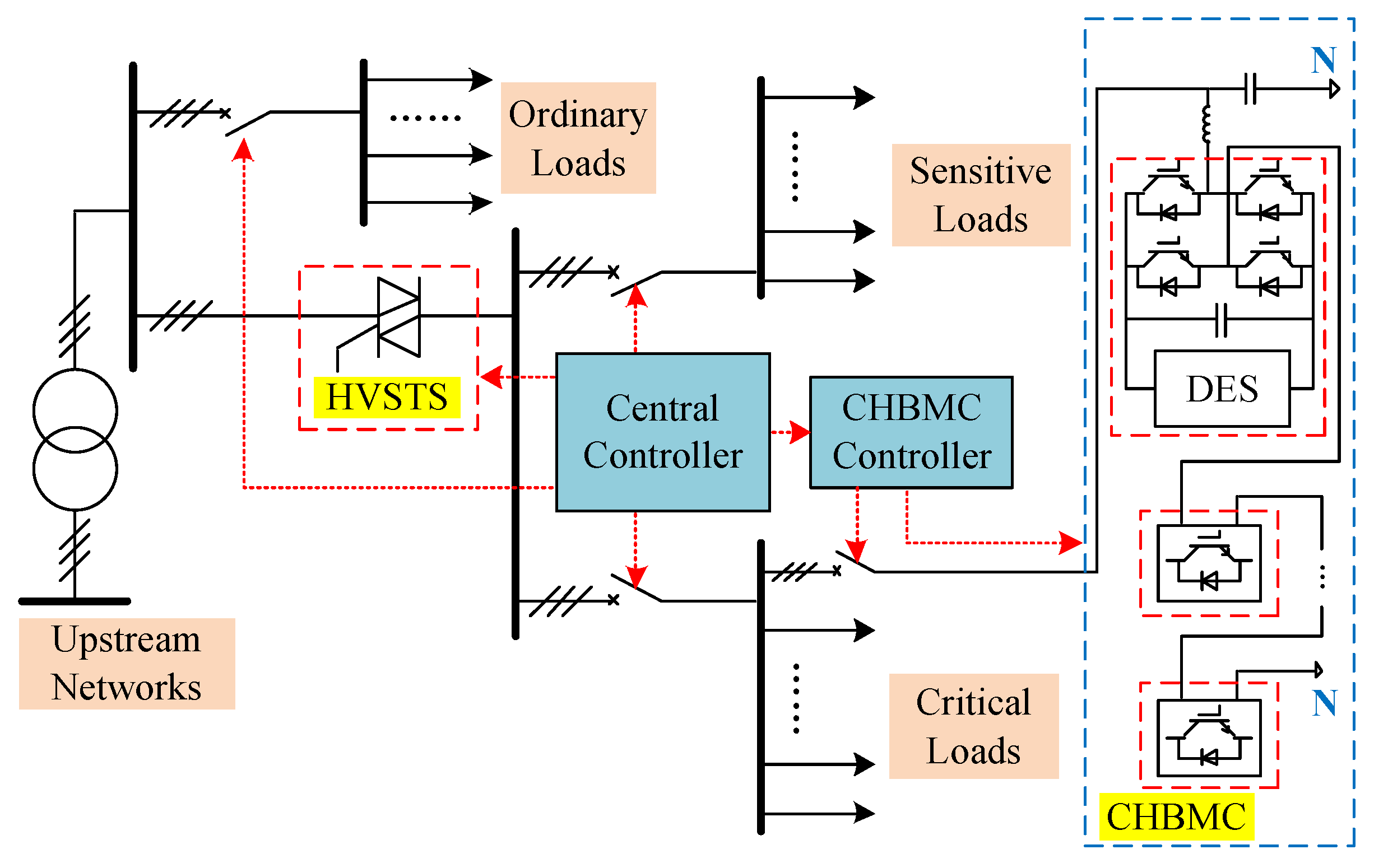
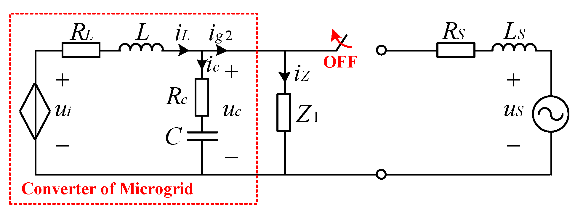
A representative single-phase configuration of a balanced network for a multi-functional microgrid studied in this paper is shown in Figure 1. The line voltage of the AC bus was 10 kV and the upstream switch that interfaced the converter and critical/sensitive loads to the utility was a set of high-voltage thyristors clusters (HVSTSs). With an LC filter, a cascaded H-bridge multi-level converter (CHBMC) was employed because of its advantages of modular design, easy expansion, and high fault tolerance in high-voltage or large-scale microgrids [31]. Each cascaded H-bridge contains independent DC energy sources, i.e., distributed photovoltaic, fuel cell, biomass, super/ultra capacitor, or any other energy source [32,33]. A central controller dominates the power flow and decides the operation mode of the CHBMC by sending a transfer command to its controller.
It should be noted that unbalanced power cannot be regulated owing to the intrinsic feature of CHBMC that there is no flow path for the zero-sequence current [33]. Furthermore, a compulsory disconnecting method was employed for the period between the UC mode and SA mode if the semi-conducting switch could be turned off when receiving the “off” signal, which is in reference to [34]. Hence, before introducing the main research contents of this paper, the following assumptions are proposed:
- The three-phase system and local load are symmetrical;
- The fault detection and HVSTS operation time is short and can be ignored;
- The capacity of energy storage is sufficient to meet the load’s demand.
2.1. Control Strategy for the UC Mode
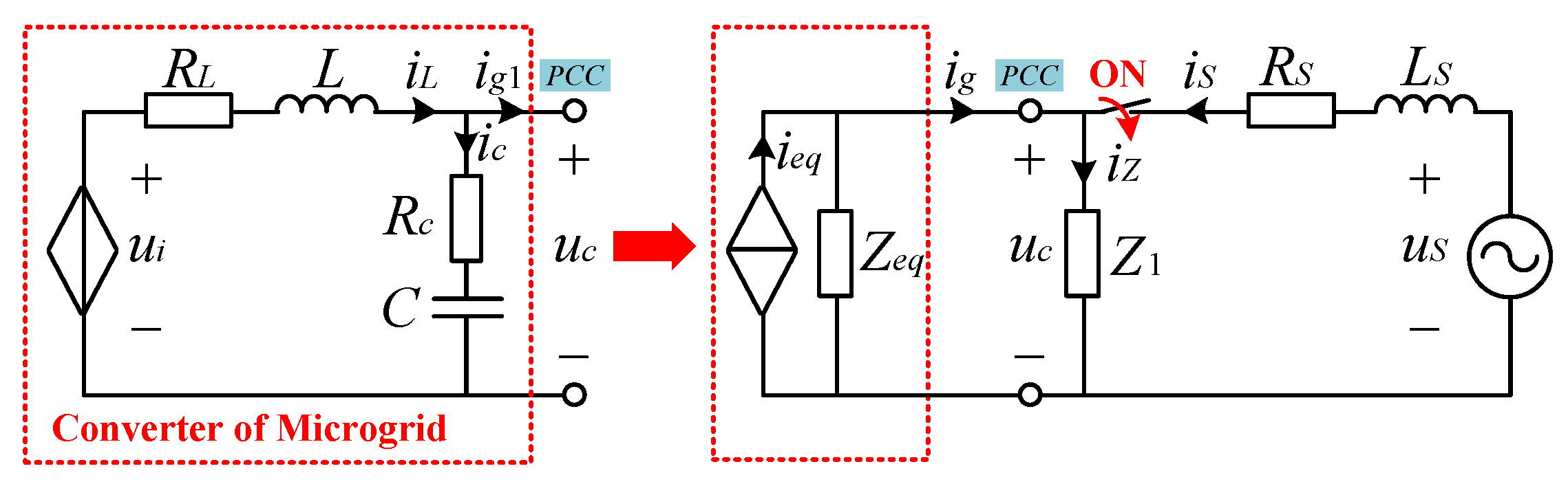
The analysis was initiated by looking at the UC mode shown in Figure 2, which is a representation of a three-phase balanced circuit. ui is the output voltage of the phase leg. HVSTSs are closed and the point of the common coupling (PCC) voltage uc is dictated by the grid voltage us with the equivalent resistance Rs and reactance Ls dominantly. Local loads Z1 are powered from the utility and the converter takes charge of delivering/absorbing energy to/from the host network as a controlled current source (CCS) by injecting an active/reactive current ig1. The expression of ig1 is shown in Equation (1).
where ZL(s), Zc(s), and Zs(s) are the equivalent impedance of the filtering inductor branch in the net frame of Figure 2.
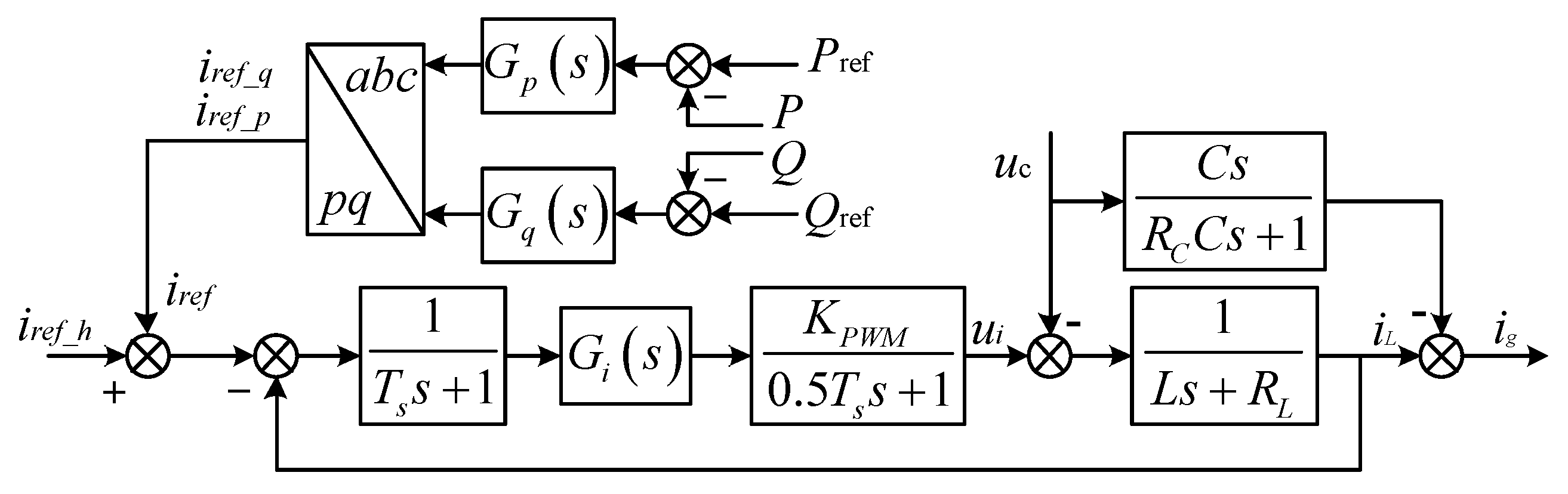
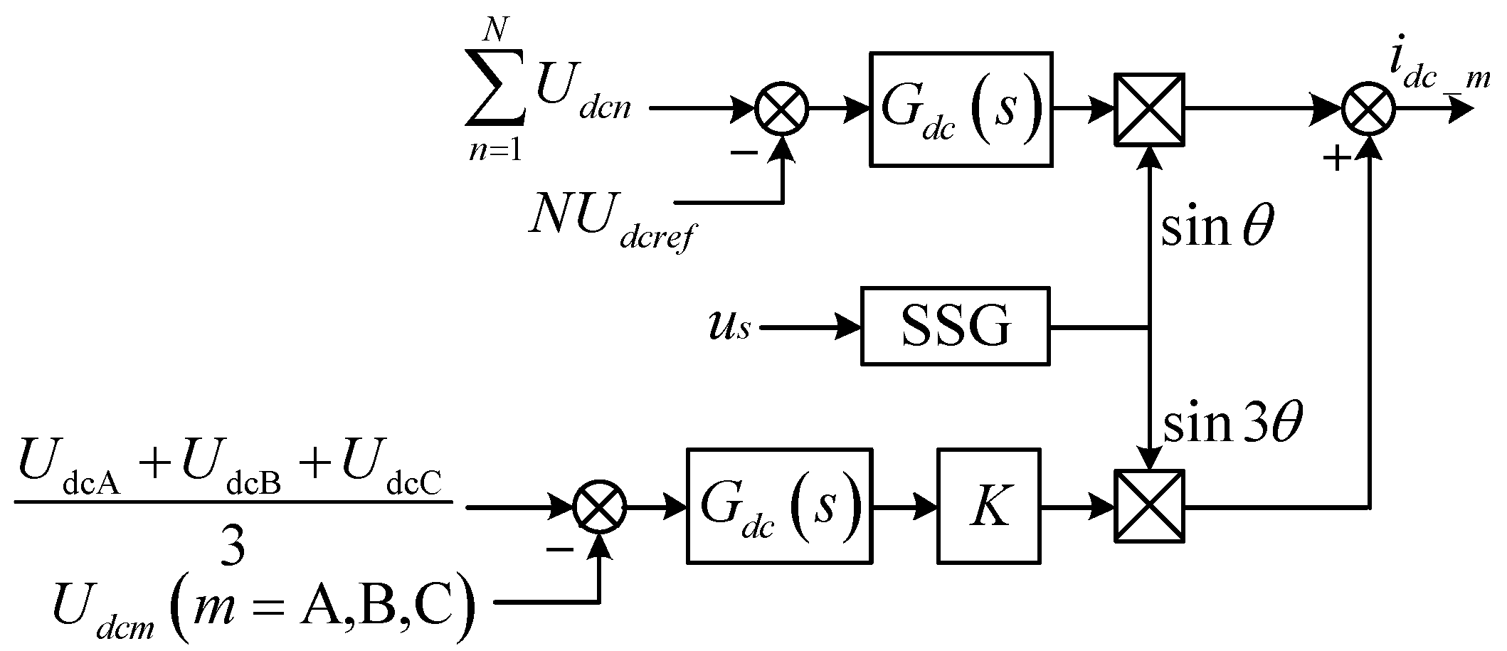
With the sampling delay and inertia characteristics of the PWM control, Figure 3 shows the traditional control block with an outer active/reactive power loop and inner inductor current loop [15]. The inner inductor current loop with controller Gi regulates the current obtained from the controllers of Gp and Gq. For the harmonic suppression, the harmonic component iref_h can be calculated, separated, and added to the referring instruction of the current loop. It is worth noticing that stability of the DC voltages is the basis for the normal operation of the CHBMC. Thus, the modifying component idc_m obtained in Figure 4 is superposed further to form a multi-closed-loop structure, where θ is observed by a Synchronous Sinusoid Generator (SSG).
2.2. Control Strategy for the SA Mode
Figure 5 shows the equivalent circuit of the SA mode. HVSTSs are open so that the microgrid and local loads are fully disconnected from the main grid as an insular scenario. The desired terminal voltage and frequency for the load Z1 are offered by the CHBMC as a controlled voltage source (CVS) to ensure the immunity of the critical loads to power interruptions and grid faults. The injection current ig2 is expressed as Equation (2), which is also the load current iz.
The traditional dual-loop control structure for the converter to operate as a voltage source is shown in Figure 6, where the outer voltage loop supplies reference for the inner inductor current loop [35]. The load current iZ(ig) is usually sensed and added to the reference with coefficient Kz of the current control loop to improve the quality of the PCC voltage [36].
2.3. Instability of the Transition Modes
2.3.1. From SA Mode to UC Mode
When the microgrid system is about to reconnect to the utility from SA mode, it experiences a current surge and backflow if deviations exist in the amplitude, phase, or frequency between the PCC voltage and the utility voltage before turning on the HVSTS. The so-called pre-synchronization [17,30] has been well studied to synchronously adjust the output voltage of the converter, because of its controllable property as a voltage source. After reconnecting to the utility, the operation mode of the converter changes to inject the desired current. However, the referring instruction of the inner current loop undergoes a certain degree of step changes during the utility reconnection.
2.3.2. From the UC Mode to SA Mode
Likewise, before disconnecting from the utility, whether planned or not, the equivalent load of the converter can be observed as a parallel combination of local loads and the utility with a small impedance in total. When the microgrid system is transferring from the UC mode to SA mode, the equivalent load impedance is changing into the ones of local loads. If the control structure switches from CCS to CVS in the instant of mode transition, the output of the current loop inevitably reaches the limit as the input instructions of the two structures are different, which also leads to a surging current, a worsening of the PCC voltage, and affects the normal operation of the load [37].
3. Unified Inner Loop Based on the 2-DOF Theory
3.1. The 2-DOF Theory
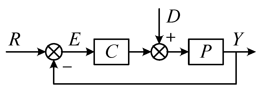
Regarding the conventional feedback structure shown in Figure 7, the performance of instruction tracking and disturbance rejecting cannot be optimal at the same time, which is the so-called single degree of freedom. On the contrary, the above-mentioned control targets can be achieved through the 2-DOF control by setting an extra feedforward or feedback path to decouple the input, output, and interference signals [24].
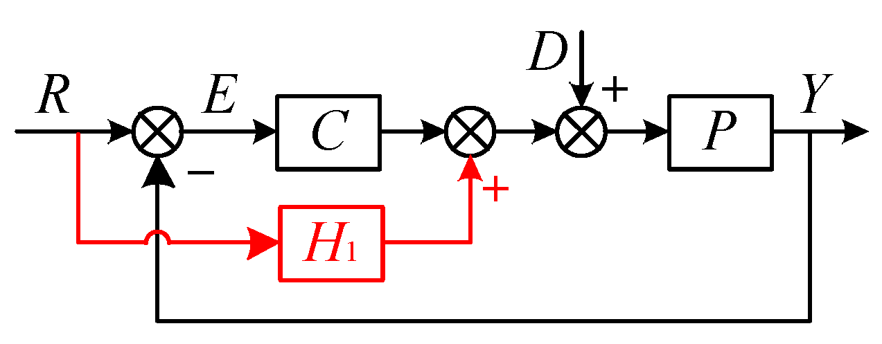
Figure 8 shows the block diagram of the 2-DOF control with reference to feedforward instructions, rather than introducing a high frequency or abnormal distortion of the feedback signal, which accommodates the closed-loop control system that contains unintentional noises.
The transfer function can be expressed as:
where R(s), D(s), and Y(s) represent the command, disturbance, and output variables, respectively. H1(s) is the feedforward compensator of input signal R(s), while C(s) is the function of the feedback regulator and P(s) is the controlled plant. If there is no error in the plant model, the immunity of the output Y(s) to disturbance D(s) simply relies on the parameters of C(s). The tracking performance can be further enhanced through the feedforward compensator after the parameters of C(s) are optimized according to the performance of anti-disturbance. In this way, Y(s) is regulated by the 2-DOF algorithm. The expression of H1(s) can be produced on the principle that the error E(s) in Equation (4) is a constant of zero (tracking the command perfectly) if the model of the plant P(s) is invertible, as in Equation (5).
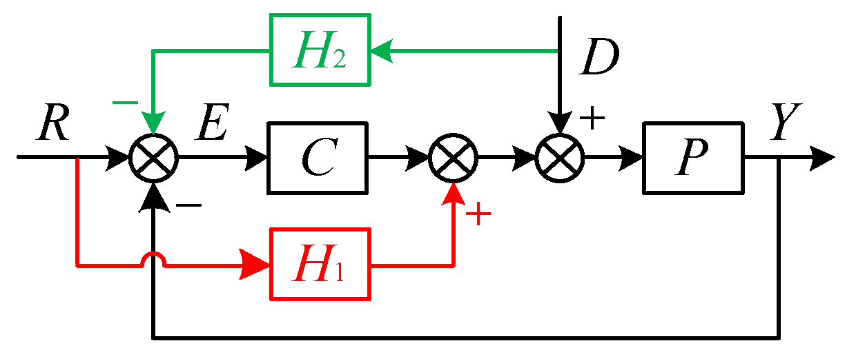
However, the anti-disturbance performance of the system, as shown in Equation (3) can be enhanced by increasing the proportional gain of C(s), which causes the poles of the closed-loop transfer function to approach the virtual axis and influence the stability. In the present study, to respect the generalized design concept of the 2-DOF control structure, a feedforward compensator H2(s) for disturbance rejection is also employed, as shown in Figure 9.
Equation (3) can be adjusted into:
If H2(s) ≡ [C(s)]−1, then the influence of D(s) on Y(s) can be ignored. The performance goals are for all the frequencies and can completely suppress the effects of disturbance on the output and make the output perfectly track the command.
3.2. Construction of the Proposed Strategy
As discussed in the above sections, the output variables cannot precisely follow mutating instructions for the inner loop, and current mutations and power oscillations may occur, accompanying the alteration of the control structures. Therefore, it can be deduced that the inner current loop becomes the nucleus for the operation of different modes, while the PCC voltage can be set as a disturbance of the forward path that fluctuates with ambient conditions.
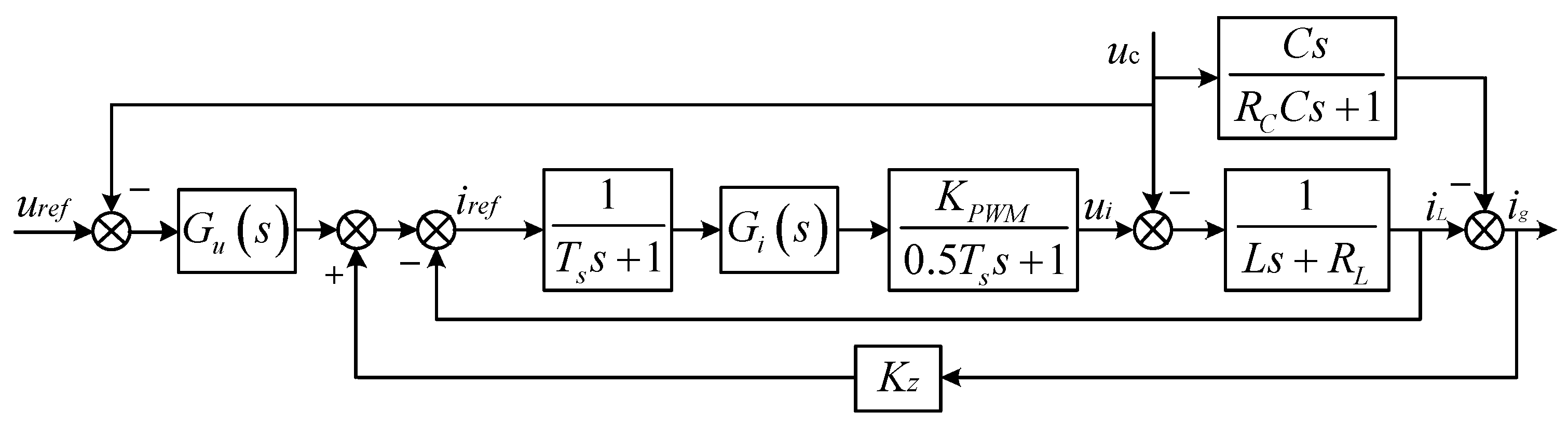
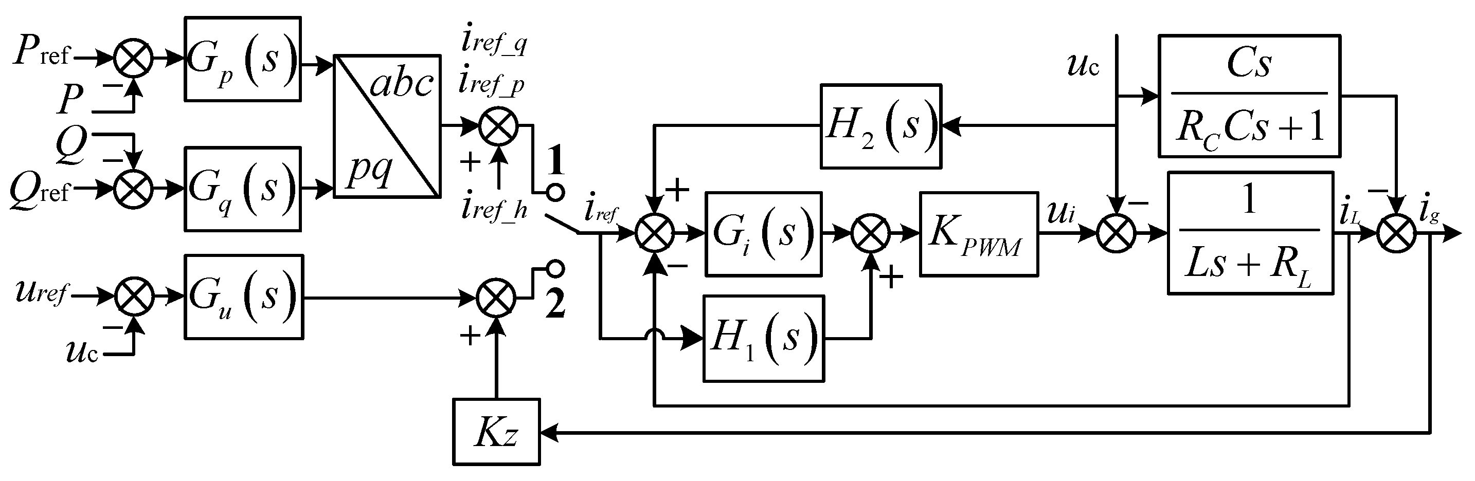
The inner current loops shown in Figure 3 and Figure 6 are exactly the same, while the input instructions from the outer loops are different. Additionally, the instability of the microgrid system during the transition modes is attributed to the mutation of the inner current instructing signal. In light of this, a unified inner loop control strategy based on a generalized 2-DOF theory is designed in this paper, as shown in Figure 10. Hence, the seamless transfer between operating modes can be facilitated more accurately for both a disconnection and reconnection from the utility grid, by maintaining the structure of the inner current loop, and the transfer modes of the microgrid are turned into the infrastructure switching of the outer loop.
Owing to the high switching frequency, the inertia characteristics of the converter can be approximately equivalent to a common proportional component with the gain KPWM, while the injecting current Ig can be reasonably assumed to approximate the inductor current IL because the capacitor current of the LC filter is much smaller, in comparison to the injecting current Ig. The transfer function of the output current IL, with referring instruction IR and disturbance UC, can be expressed as:
where Gi generally takes the proportional-integral (PI) controller. The error function E(s) between IR and IL is:
Theoretically speaking, Equation (8) should remain valid in whatever form of IR and UC if IL(s) ≡ IR(s). Henceforth, the expressions of H1(s) and H2(s) can be formulated as Equation (10).
where KP and KI are the proportional and integral gains of the PI controller.
It is indicated in Equation (10) that H1(s) is exclusively relevant to the plant model, while the structure of H2(s) depends on the parameters of Gi. To solve the improperness of the inverse model transfer function, a first order low-pass filter is contrived to yield a modification for H1(s), so that the problem of interference amplification caused by the differential can be suppressed and the dynamic performance of the inner control section can be improved with λ. H1(s) is adjusted as Equation (11):
where 1/λ represents the cutoff frequency of the filter, and then a perfect reference tracking capability within an expected frequency range [0, 1/λ] will be provided.
3.3. Design of the Proposed Control System
The existence of the equivalent loss resistance RC in the LC filter contributes to reinforce the damping effect on the resonance, as well as the stability of the system. If the system is stable when ignoring the equivalent loss resistance, then it should be stable for any other scenarios. Therefore, in the subsequent discussion, RC is ignored. Table 1 shows the values of the key parameters of the plant model.
It can be observed in Equation (10) that there is no coupling between H’1(s) and H2(s), while H2(s) is merely related to the PI controller. Thus, these two feedforward compensators can be separately and independently designed. Giving priority to the tracking performance and adequate amplitude/phase margin, the unified inner current loop studied in this paper is designed on the basis of a first-order system before subsequent research is conducted.
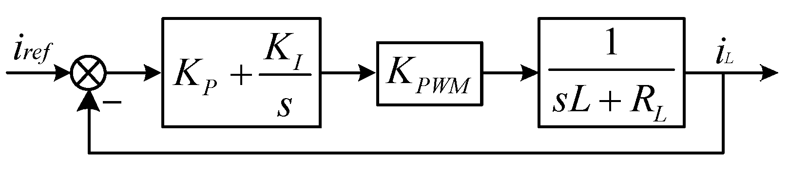
If taking no account of the disturbance signal uc, the inner current loop in Figure 10 can be transformed into a simplified structure with unitary feedback, which is shown in Figure 11.
The equivalent transfer function of the inner current loop is expressed as:
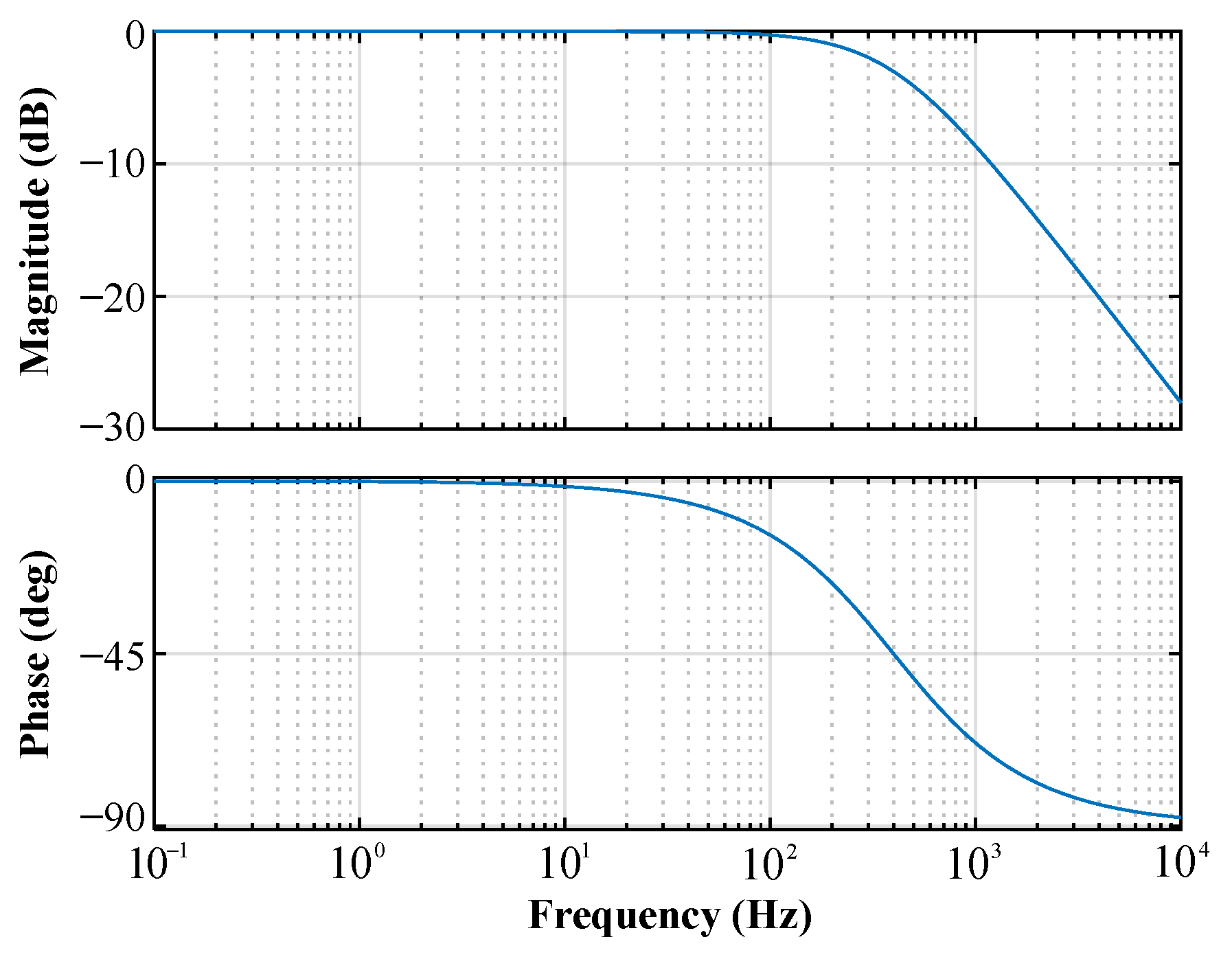
Considering the proportional gain KPWM of the studied CHBMC as 1, then the parameters of the PI controller are designed as KP = 2 and KI = 5, referring to the principle of a typical first-order system. A corresponding bode diagram of the closed-loop transfer function displayed as Equation (12) is shown in Figure 12, where the system is stable in all bands of frequencies.
The feedforward compensator H2(s) of the disturbance signal can be exclusively expressed as:
In Figure 12, it is also indicated that error of tracking exists in the middle-frequency band and the error increases along with the frequency. If the load in the micro-grid is nonlinear, the tracking accuracy of the high-order harmonic signals is not ensured, which explains the necessity of the input feedforward compensation of H’1(s) to eliminate the problem of error.
The closed-loop transfer function from iL to iR with Equation (12) is modified as:
According to the Routh Criterion, the system derived from Equation (14) is constantly stable with λ > 0, and the greater the value of λ, the more stable the system. The transfer function from the error to IR can be expressed as:
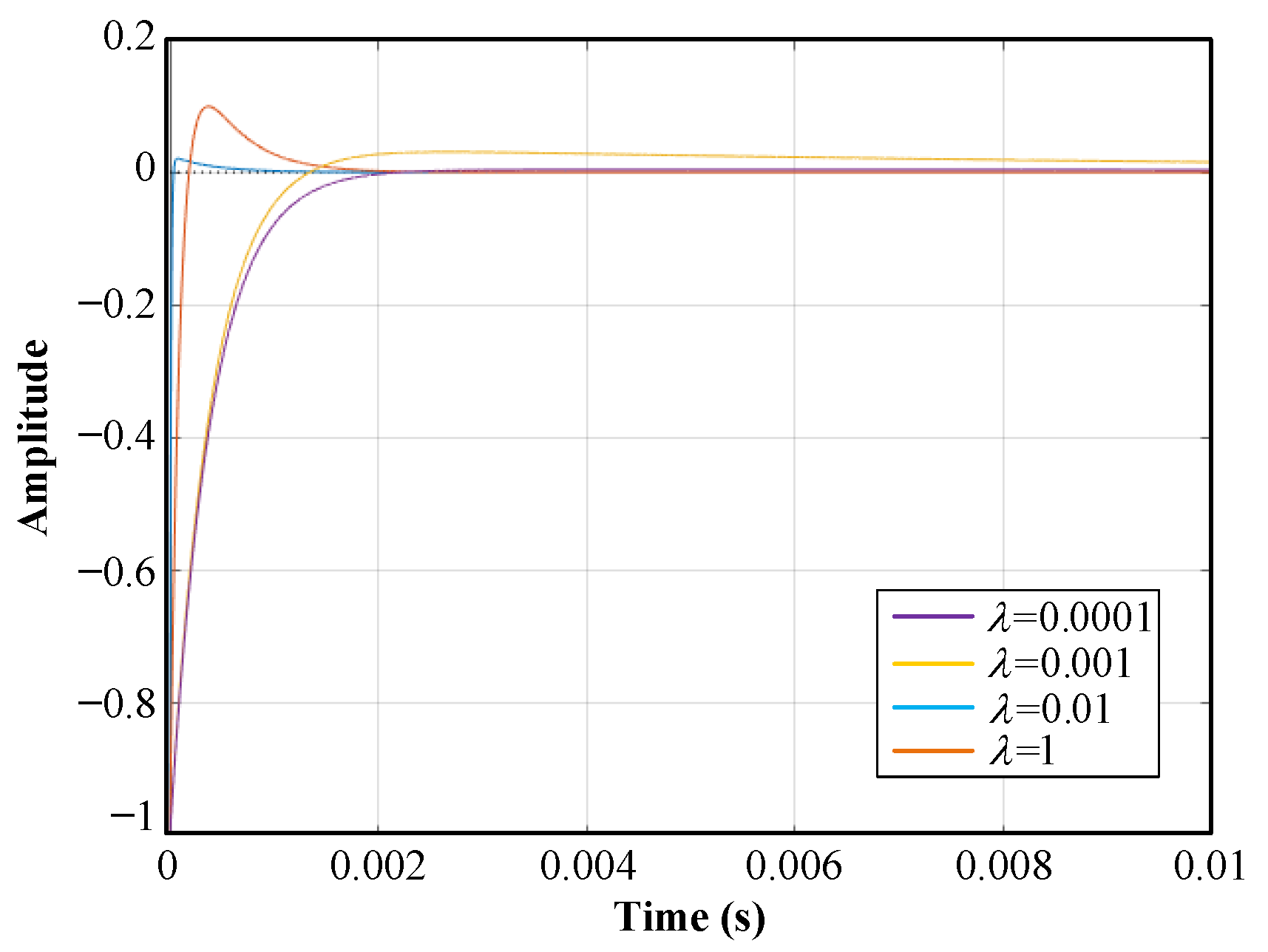
In order to simulate the sudden change of input instructions in the inner loop during the transfer mode of the microgrid, the curves of the unit-step responses with λ set at 0.0001, 0.001, 0.01, and 1, respectively, are shown in Figure 13.
When λ = 1, the overshoot is eliminated, but the increasing time is longer than 10 ms, which is almost half of the fundamental cycle and far beyond the time tolerated by the vast majority of the sensitive load. Although it experiences a slow overshoot and fast dynamic adjustment time of approximately 0.5 ms when λ is 0.0001, a small value of λ reduces the decline of stability. Thus, the value of λ in this paper is selected to be 0.001 as a tradeoff and the whole regulating time is less than 1 ms.
The input feedforward compensation H’1(s) is expressed as:
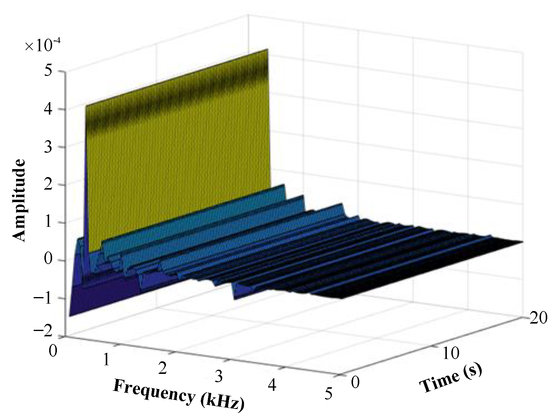
In order to verify the tracking accuracy of the sinusoidal signal in a steady state, a sinusoidal signal with an angular frequency ω is assumed to be equal to IR, and the error function in the frequency domain can be expressed as:
The error function in the time domain through the inverse Laplace transformation can be expressed as:
The relationship between the error and angular frequency and time is shown in Figure 14. It can be observed that the error peak value is restricted within the range of −0.02~0.04% (maximum at the frequency of 350 Hz), which is totally acceptable in practical applications. Moreover, the error gradually decreases as the frequency increases, while the error basically remains unchanged for the same frequency as time progresses.
Likewise, the same results can be obtained for the cosine signals. Thus, it can be concluded that the unified control structure of the inductor current feedback proposed in this paper can ensure good tracking accuracy of the AC instructions in a steady state.
3.4. The Influence of the Changing Plant Parameters
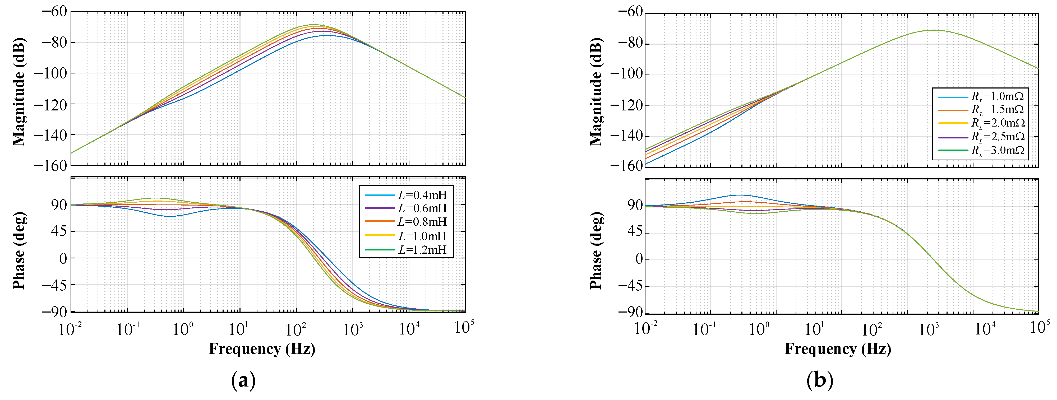
Due to the influence of the external working environment, such as temperature, electromagnetic radiation, and operation aging, the parameters of the converter components have a certain positive or negative deviation, which affects the control precision or stability even more. For the studied strategy in this paper, the input feedforward compensator H’1(s) is vulnerable to the change of plant parameters, which influences the tracking performance. The error function can be expressed with ΔL and ΔRL as:
where ΔL and ΔRL are the parameter offsets of the filtering inductor and its equivalent loss resistance. Figure 15 shows the bode diagram of Equation (19) with different ΔL and ΔRL, when the variation of both offsets are considered as −50%, −25%, 0, +25%, and +50% of the initial values. It can be observed that the characteristic of the amplitude/phase frequency has no obvious change with the change of L and RL in the frequency range of the AC signals, while the speed of attenuation decreases minimally with the increase in L in the frequency range under 1 kHz. Ultimately, the stability and robustness of the proposed strategy against the model uncertainties of the converter are proved.
4. Simulation Results and Experimental Verification
This section verifies the feasibility and correctness of the proposed strategy through simulation and a low-voltage prototype experiment with the same control structure, but less H-bridges in each phase. The parameters of the studied system are listed in Table 2, respectively as supplementary to Table 1.
4.1. Simulation Results
For comparison and substantiation, two traditional approaches, i.e., direct transition and zero-current (current of loads) transition, are adopted with three common kinds of load, i.e., resistance (R) representing the heating devices, resistance and inductance (R-L) representing the induction machines, and nonlinear load representing the rectifiers. In addition, harmonic suppression and reactive power compensation are implemented, once CHBMC is operating in the UC/CCS mode. The simulation model is studied through the MATLAB/SIMULINK toolbox. Without a loss of generality, the mode switches at the simulated time of 0.325 s, when the voltage of the utility meets its peak value. All the following waveforms are displayed and analyzed with the ones of phase A as representatives.
4.1.1. From the UC Mode to SA Mode
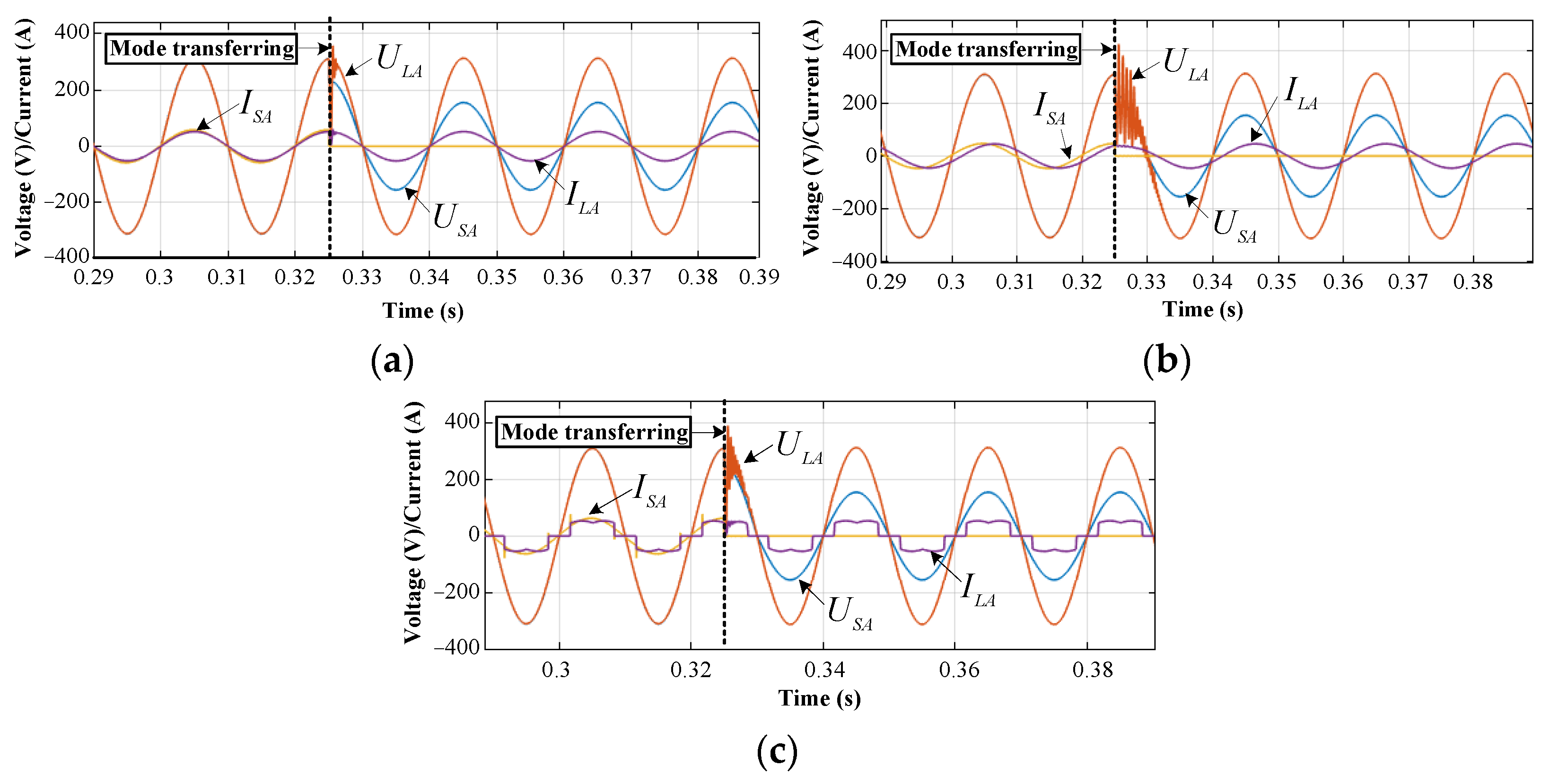
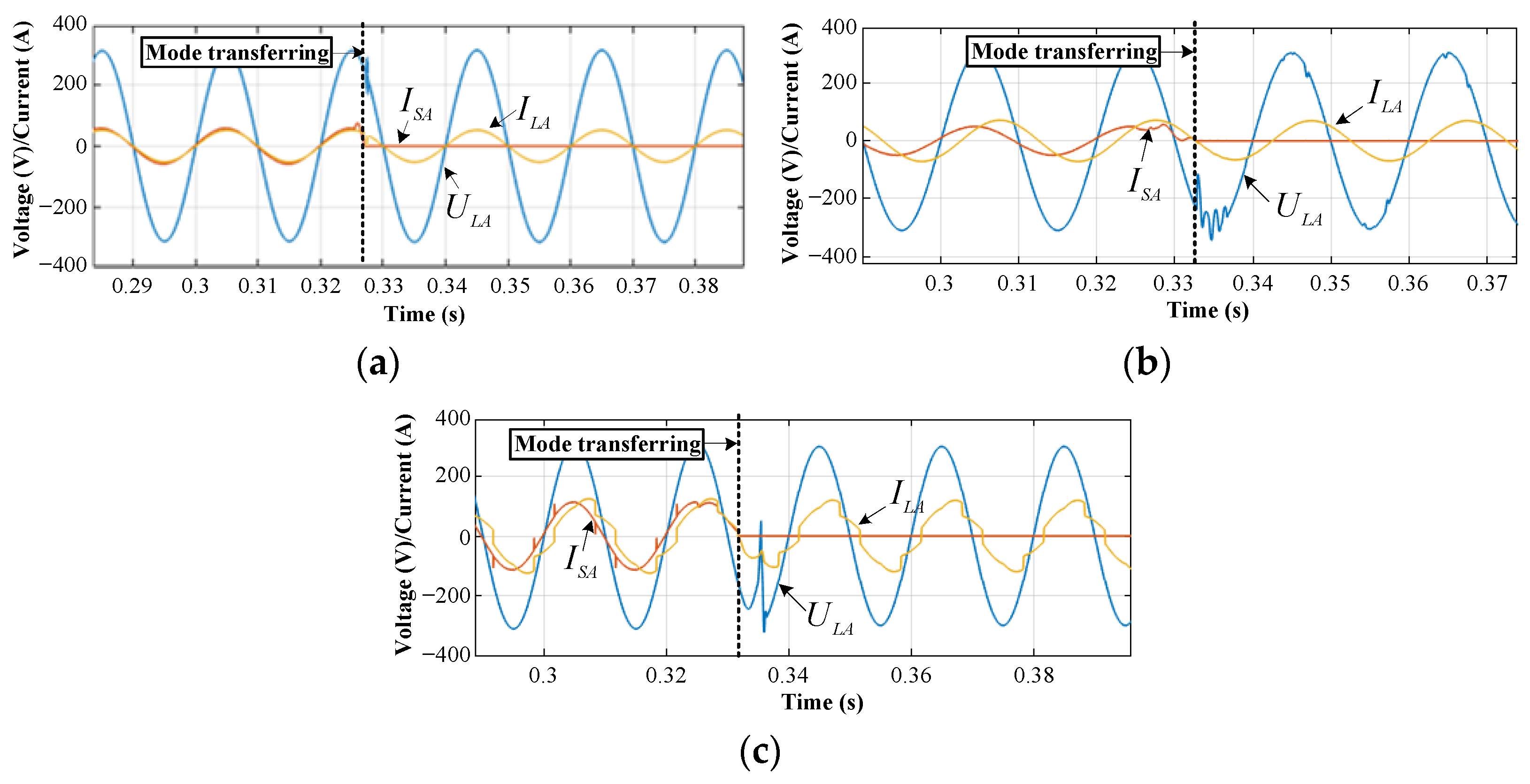
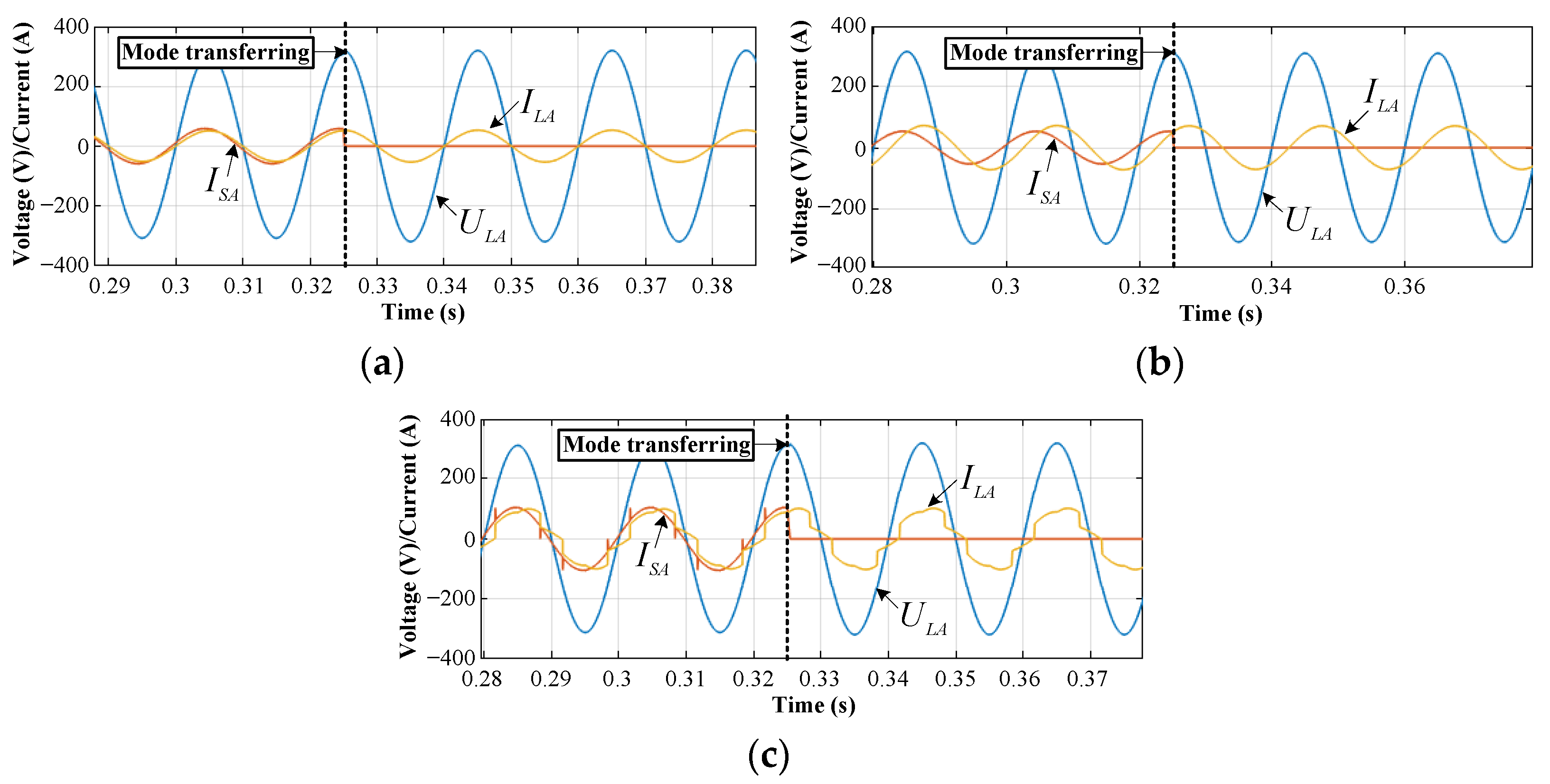
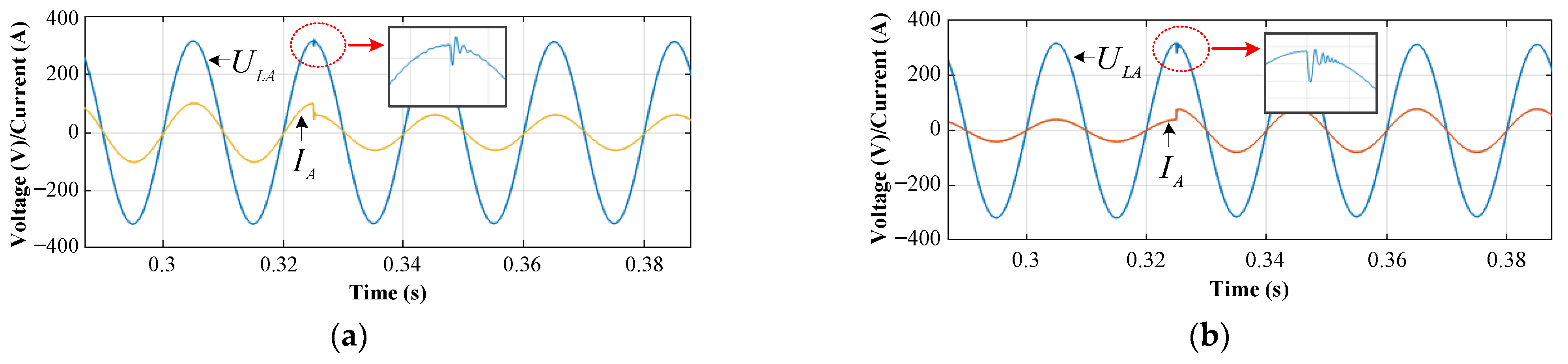
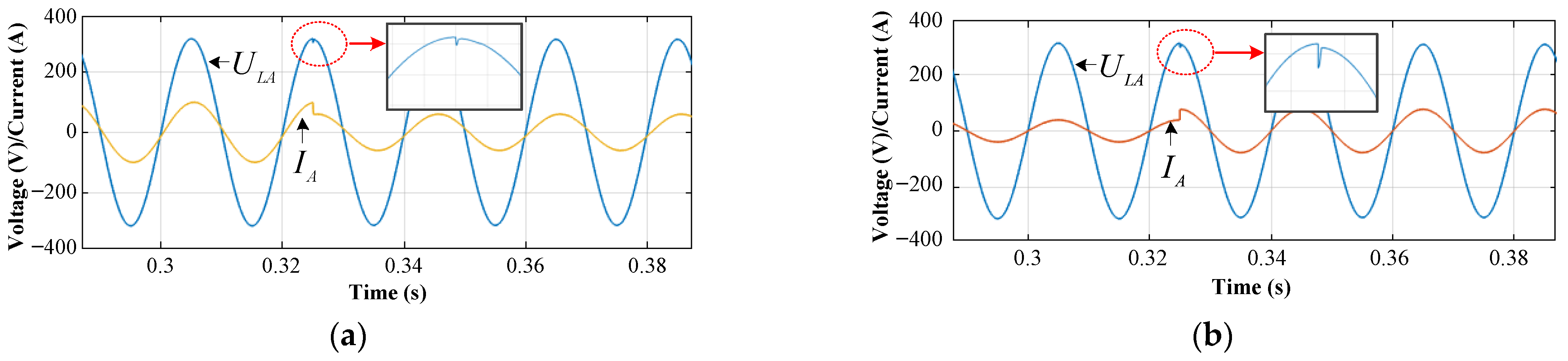
Figure 16 shows the simulation waveform of CHBMC when switching directly after receiving the mode transfer command from the central controller with three different types of load. Due to the different control structures of the CHBMC controller in different working modes, the direct transition from the UC/CCS mode to SA/CVS mode leads to variances in the input of the inner current loop, causing a short, but unneglectable, oscillation of the PCC voltage ULA. Similarly, it fails to solve the above-mentioned problems if the control structure transfers after the load current ILA exceeds zero. Although there is no short oscillation, the zero-current transition still distorts the output voltage waveform in varying degrees, which is presented in Figure 17.
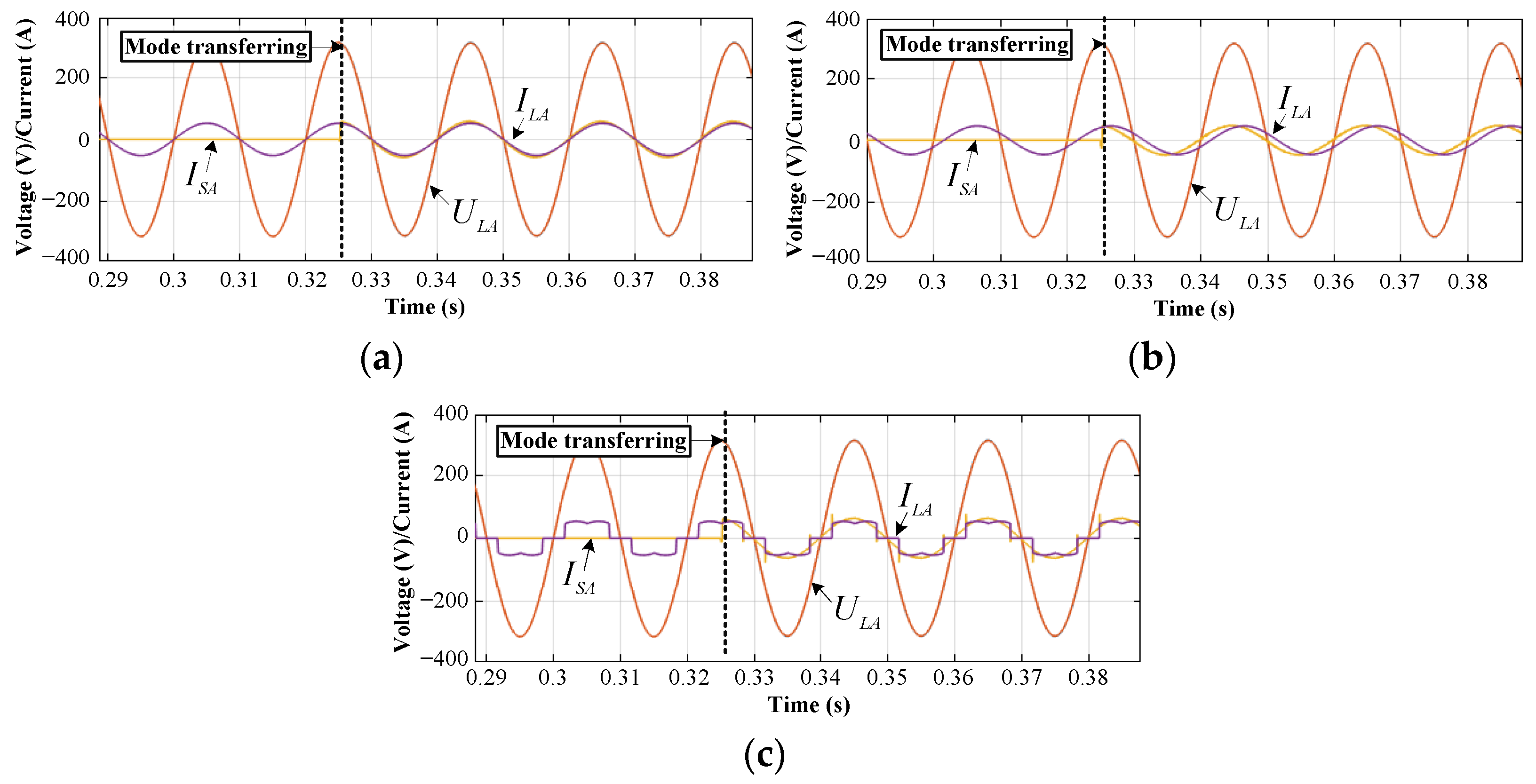
It can be deduced that the essential reason for the above-mentioned problem is that the current output of the converter cannot rapidly track the reference variation, because of the inherent inertia of the plant model. Then, undoubtedly, the output voltage cannot meet the actual control requirements. However, Figure 18 shows that mode of transition has a significant influence to modify the instant using the strategy proposed in the present paper. After receiving the mode switching instruction from the central controller, the CHBMC immediately alters its working mode. The PCC voltage ULA is continuous, with no interruptions or oscillations. The utility current ISA experiences no surge before decreasing to zero, and the load current ILA retains its normal state without distortions.
4.1.2. From the SA Mode to UC Mode
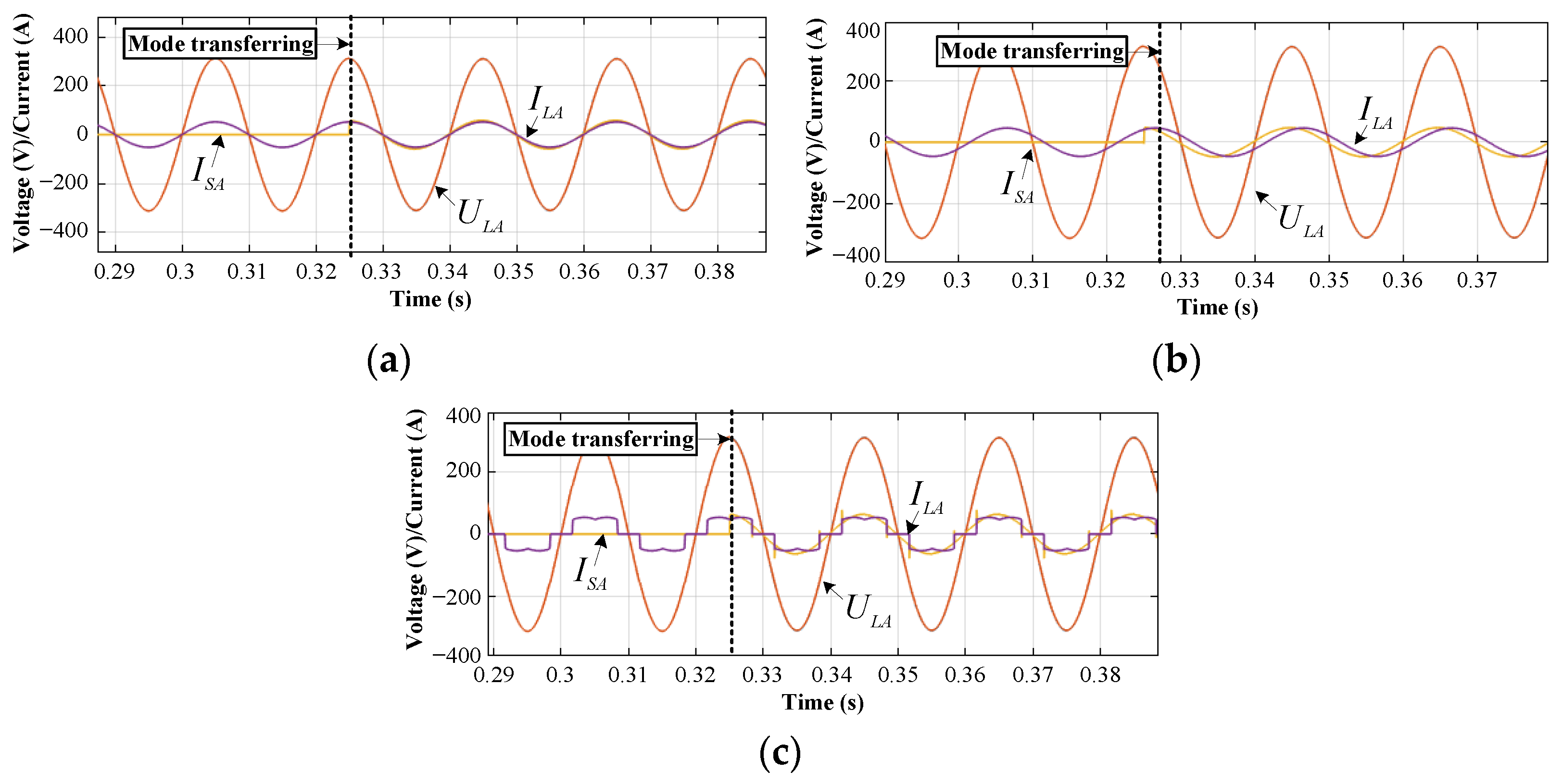
To ensure a constant supply of high-quality power, the CHBMC should compensate the reactive power or suppress the harmonics of the grid current, once it reconnects to the utility in the SA mode. Under the circumstances, the problem of reference saltation is still inevitable. For the convenience of the current analysis, it is assumed that the output voltage of the CHBMC in the SA mode was synchronized with the utility, and the interconnection switch was turned off before the mode transition occurred at the simulated time of 0.325 s.
The simulation results of direct switching from the SA/CVS to UC/CCS mode is shown in Figure 19. Despite there being no disharmony for the PCC voltage ULA and load current ILA, there is an obvious fluctuation in the grid current ISA, which indicates that the output current of CHBMC also contains this component, and the fluctuation is positively correlated with the amplitude of the current instruction. On the contrary, the simulation results of the proposed strategy are presented in Figure 20. It can be observed that the grid current ISA barely has any fluctuations at the switching point, and the reactive power and harmonic component can immediately be compensated, which theoretically proves the feasibility of the control strategy proposed in the current paper.
4.1.3. Saltation of the Input for the Inner Current Loop in the Steady Operation Mode
On the other hand, the mode transfer is infrequent in the entire operation cycle of the microgrid system, of which the process simply lasts for several milliseconds. Contrastingly, the steady operating state in the UC or SA mode is much longer and it is of a greater possibility that a sudden change in the reference or supplied load will be experienced. The simulation results are compared in Figure 21 and Figure 22 by means of a traditional dual closed-loop with PI controllers and a proposed unified strategy, respectively, when the input signals of the inner current loops saltate. To be more similar to the practical application and for the ease of analysis, two typical situations are simulated in this subsection: where the injecting current reference decreasing in the UC mode, and the resistance load increasing in the SA mode.
As shown in Figure 21, when the input signal of the inner current loop changes, the PCC voltage ULA appears to oscillate, whether in the UC/CCS or SA/CVS mode. Meanwhile, the voltage oscillation also creates an unstable state, for a short period of time, for the injecting current IA. In Figure 22, the oscillation or instability of the PCC voltage and the injecting current are noticeably alleviated in both the UC/CCS and SA/CVS modes. In addition, the transient processes in both modes are restricted to 50 μs and exert no influence on the power supply of the load.
4.2. Experimental Verification
To further verify the theoretical analysis and simulated results, an experimental prototype was built in a laboratory, while the parameters were the same as those in the simulation model. The converter was built with dual-IGBT modules (FF300R06KT4 from Infineon) and the control strategy was realized by DSP (TMS320F28335 from Texas Instruments) and FPGA (EP3C25E144C8 from Altera). The DC energy storing devices were created with super-capacitors and the load consisted of resistance and inductance as the simulations in the previous section.
4.2.1. Operation Mode Transition
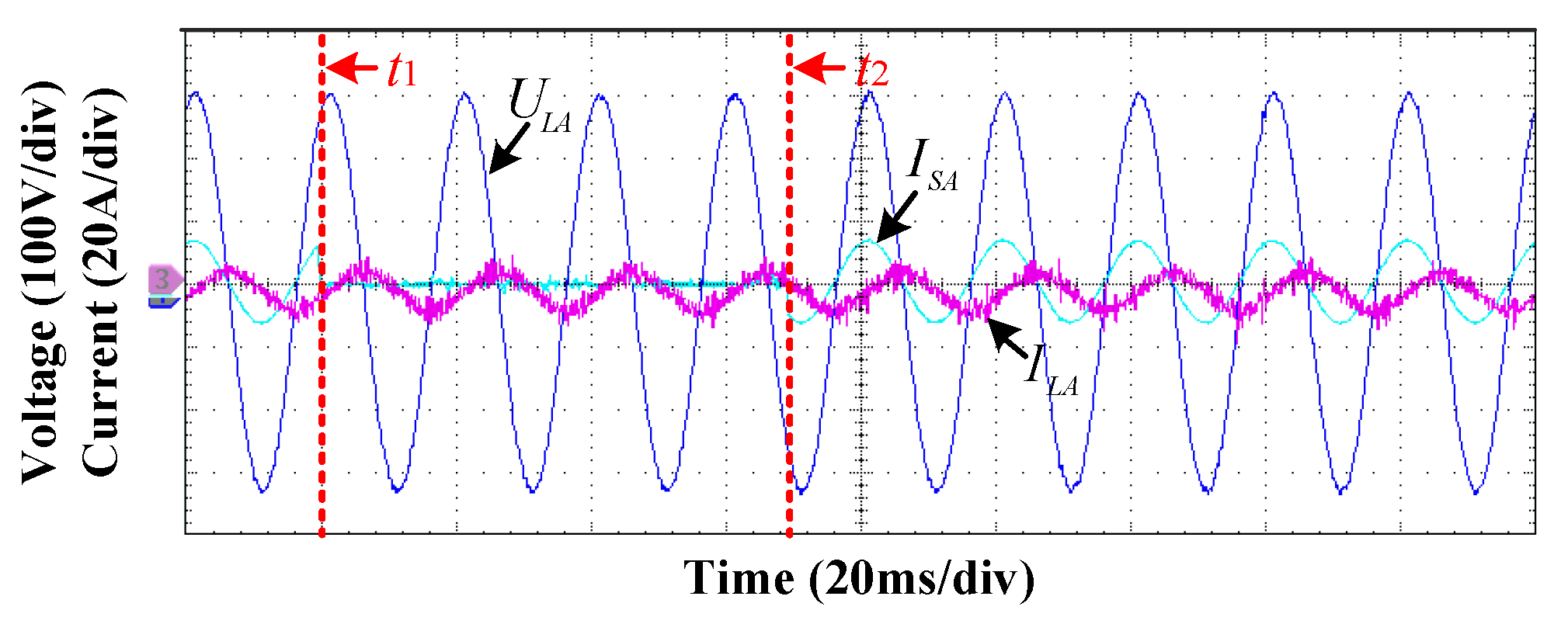
Figure 23 shows the experimental results of the modes transfer between one another. Initially, the microgrid system was in the UC/CCS mode. At the time of t1, it converted to the SA/CVS mode, and back to the UC/CCS mode at the time of t2. Noticeably, the load reactive power was compensated to ensure that the power grid current was a unit power factor, while the super-capacitors on the DC side were charged to a set value when the system was in the UC/CCS mode.
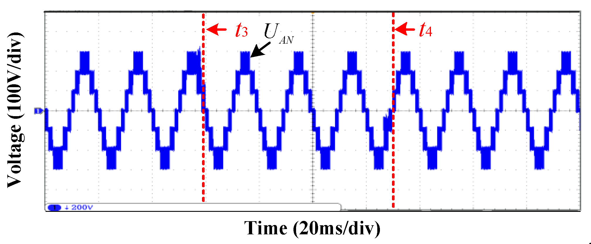
Accordingly, the AC output voltage between the H-bridges of phase A and the neutral point N is depicted in Figure 24, where the system transfers from the UC/CCS to SA/CVS modes at time of t3 and returns to the UC/CCS mode at the time of t4. Therefore, it can be observed that the continuity and quality of PCC voltage ULA are well guaranteed, while the grid current ISA experiences no surge or oscillation, and the load current ILA is basically not affected by the mode switching. The performances can be assessed by the fact that the mode transitions are seamless and the proposed strategy keeps the load protected from any disturbances.
4.2.2. Saltation of the Inner Current Loop Input in a Steady Operation
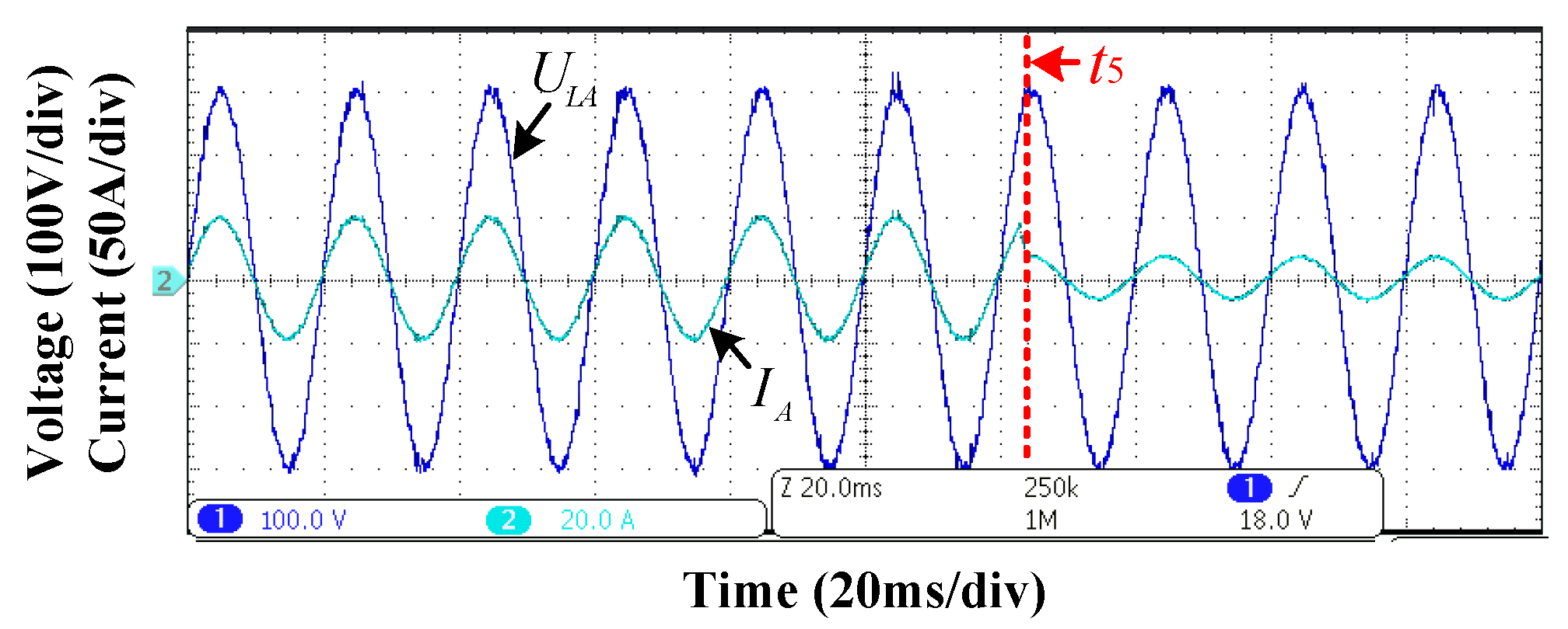
Figure 25 shows the experimental result that the current instruction for injecting active power from the DC energy storing devices to the AC bus instantaneously decreases at time of t5 in the UC/CCS mode.
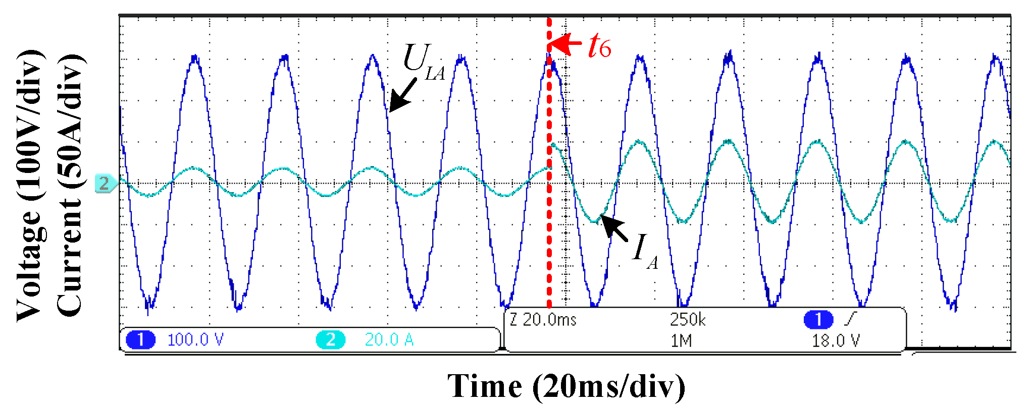
Figure 26 shows that the local loads increases at the time of t6 in the SA/CVS mode. By observing the experimental waveforms, it is evident that PCC voltage ULA and the injecting current IA remain unaffected and the transient processes are milder and negligible when the instruction of the current inner loop varies in the two steady operation modes.
4.3. Limitations
Due to the inadequacy of the experimental conditions, the theoretical correctness and practical feasibility of the proposed strategy were simply simulated and verified in the low-voltage system of 220 V, while it was originally designed for a high-voltage system. Thus, the experiments with a 10 kV prototype can be carried out in the next stage, after the necessary re-configuration of the high-voltage system, which exhibits differences, such as component selection, insulation distance, and a protection mechanism, when compared to the low-voltage system.
In addition, the test conditions in this study were relatively ideal, and some special situations may occur in practical applications and are worth studying, for instance:
- (1)
- Mechanism for handling the faults of the load side during modes of transition and for restoring the voltage in the shortest time;
- (2)
- Redundancy configuration of H-bridges in a cascaded multilevel topology;
- (3)
- Measures to improve the inherent effects of sampling and control delay in digital control systems.
In general, there are still problems and a more sophisticated strategy shall be researched further in future studies.
5. Conclusions
For the multi-functional converter in a microgrid system, the transition between the control structures for different operating modes was a hindrance, which stemmed from the contradiction of input, output, and disturbance in the control diagram.
In this paper, the diversity and connection between the control structures in different operating modes were studied and a unified inner loop based on the 2-DOF theory was introduced. With the proposed method, all the operating modes of the converter in the microgrid can share the same inner loop, so that the switching of the operation modes can be altered to reflect the change of the inner referring instructions, rather than a reconfiguration of the whole control structure. Proper tracking and interference rejection performances were fulfilled. Thus, coordinated functions, such as an uninterrupted voltage supply, active power regulation, reactive power compensation, harmonic suppression, and seamless transition, can be employed to ensure a satisfactory power quality for local loads. The simulation and experimental results through a low-voltage prototype model were also presented to validate the effectiveness of the proposed strategy, which provided a theoretical and practical basis for the experiment in high-voltage applications.
Author Contributions
Conceptualization, J.W., W.H. and B.W.; methodology, J.W. and W.H.; data collection and analysis, J.W.; writing—original draft, J.W.; writing—review and editing, W.H. and B.W. All authors have read and agreed to the published version of the manuscript.
Funding
This research was funded by part of the Fundamental Research Funds of the Central Universities of China, grant number 8516008300.
Institutional Review Board Statement
Not applicable.
Informed Consent Statement
Not applicable.
Data Availability Statement
Not applicable.
Conflicts of Interest
The authors declare no conflict of interest.
References
- Zhang, Q.; Zhuang, X.; Liu, Y.; Wang, C.; Guo, H. A novel control strategy for mode seamless switching of PV converter in DC microgrid based on double integral sliding mode control. ISA Trans. 2020, 100, 469–480. [Google Scholar] [CrossRef] [PubMed]
- Sahoo, B.; Routray, S.K.; Rout, P.K. AC DC and hybrid control strategies for smart microgrid application: A review. Int. Trans. Electr. Energy Syst. 2021, 31, e12683. [Google Scholar] [CrossRef]
- Cagnano, A.; De Tuglie, E.; Mancarella, P. Microgrids: Overview and guidelines for practical implementations and operation. Appl. Energy 2020, 258, 114039. [Google Scholar] [CrossRef]
- Delghavi, M.B.; Yazdani, A. A Unified Control Strategy for Electronically Interfaced Distributed Energy Resources. IEEE Trans. Power Deliv. 2012, 27, 803–812. [Google Scholar] [CrossRef]
- D’Silva, S.; Shadmand, M.; Bayhan, S.; Abu-Rub, H. Towards Grid of Microgrids: Seamless Transition between Grid-Connected and Islanded Modes of Operation. IEEE Open J. Ind. Electron. Soc. 2020, 1, 66–81. [Google Scholar] [CrossRef]
- Lo, K.; Chen, Y. Design of a Seamless Grid-Connected Inverter for Microgrid Applications. IEEE Trans. Smart Grid 2020, 11, 194–202. [Google Scholar] [CrossRef]
- Tran, T.; Chun, T.; Lee, H.; Kim, H.; Nho, E. PLL-Based Seamless Transfer Control Between Grid-Connected and Islanding Modes in Grid-Connected Inverters. IEEE Trans. Power Electron. 2014, 29, 5218–5228. [Google Scholar] [CrossRef]
- Gao, F.; Iravani, M.R. A Control Strategy for a Distributed Generation Unit in Grid-Connected and Autonomous Modes of Operation. IEEE Trans. Power Electron. 2008, 23, 850–859. [Google Scholar]
- Zhang, L.; Hou, M.; Zhu, G.; Lu, Z.; Geng, Y.; Liu, Y. Seamless transfer strategy of operation mode for microgrid based on collaborative control of voltage and current. AEPS 2019, 43, 129–135. [Google Scholar]
- Yuan, Z.; Wei, Y.; Liu, W.; Ma, H.; Yu, X.; Guo, P. Connecting and islanding universal control strategy for VSC of AC distribution grids. EPAE 2020, 40, 1–7, 304–305. [Google Scholar]
- Abadi, M.; Sadeghzadeh, S.M. A control approach with seamless transition capability for a single-phase inverter operating in a microgrid. Int. J. Electr. Power Energy Syst. 2019, 111, 475–485. [Google Scholar] [CrossRef]
- Trinh, Q.N.; Wang, P.; Choo, F.H.; Jin, C.; Pan, X.; Lee, H.H. A novel control strategy for smooth transition between stand-alone and grid-connected operations of distributed generation. In Proceedings of the 9th International Conference on Power Electronics, Korean Institute of Power Electronics, Seoul, Korea, 1–5 June 2015; pp. 1276–1281. [Google Scholar]
- Jha, S.K.; Kumar, D.; Lehtonen, M. Modified V-I droop based adaptive vector control scheme for demand side management in a stand-alone microgrid. Int. J. Electr. Power Energy Syst. 2021, 130, 106950. [Google Scholar] [CrossRef]
- Liu, H.; Zhang, W.; Sun, B.; Loh, P.C.; Wang, W.; Xu, D.; Blaabjerg, F. Seamless Transfer Scheme with Unified Control Core for Paralleled Systems. IEEE Trans. Power Electron. 2019, 34, 6286–6298. [Google Scholar] [CrossRef]
- Ganjian-Aboukheili, M.; Shahabi, M.; Shafiee, Q.; Guerrero, J.M. Seamless Transition of Microgrids Operation from Grid-Connected to Islanded Mode. IEEE Trans. Smart Grid 2020, 11, 2106–2114. [Google Scholar] [CrossRef]
- Hou, X.; Sun, Y.; Lu, J.; Zhang, X.; Koh, L.H.; Su, M.; Guerrero, J.M. Distributed Hierarchical Control of AC Microgrid Operating in Grid-Connected, Islanded and Their Transition Modes. IEEE Access 2018, 6, 77388–77401. [Google Scholar] [CrossRef]
- Lou, G.; Gu, W.; Zhu, J.; Li, P.; Zhang, X. A novel control strategy for the seamless transfer of microgrids based on disturbance observer. Int. J. Electr. Power Energy Syst. 2020, 118, 105804. [Google Scholar] [CrossRef]
- El-Sharawy, K.M.; Diab, H.Y.; Abdelsalam, M.O.; Marei, M.I. A Unified Control Strategy of Distributed Generation for Grid-Connected and Islanded Operation Conditions Using an Artificial Neural Network. Sustainability 2021, 13, 6388. [Google Scholar] [CrossRef]
- Hmad, J.; Houari, A.; Trabelsi, H.; Machmoum, M. Fuzzy logic approach for smooth transition between grid-connected and stand-alone modes of three-phase DG-inverter. Electr. Power Syst. Res. 2019, 175, 105892. [Google Scholar] [CrossRef]
- He, J.; Li, Y.W.; Munir, M.S. A Flexible Harmonic Control Approach Through Voltage-Controlled DG–Grid Interfacing Converters. IEEE Trans. Ind. Electron. 2012, 59, 444–455. [Google Scholar] [CrossRef]
- Liu, Z.; Liu, J.; Zhao, Y. A Unified Control Strategy for Three-Phase Inverter in Distributed Generation. IEEE Trans. Power Electron. 2014, 29, 1176–1191. [Google Scholar] [CrossRef]
- Lee, W.C. Cost-effective APF/UPS system with seamless mode transfer. J. Electr. Eng. Technol. 2015, 10, 195–204. [Google Scholar] [CrossRef] [Green Version]
- Shan, S.; Umanand, L. A Unified Controller for Utility-Interactive Uninterruptible Power Converters for Grid Connected and Autonomous Operations. IEEE Trans. Power Electron. 2019, 34, 3871–3887. [Google Scholar]
- Araki, M.; Taguchi, H. Two-Degree-of-Freedom PID Controllers. Int. J. Control. Autom. Syst. 2003, 1, 18–25. [Google Scholar]
- Herong, G.; Deyu, W.; Xiaoqiang, G.; Guocheng, S.; Wei, Z.; Ying, Z.; Weiyang, W. Two-degree-of-freedom current regulation of grid-connected inverters in microgrid. In Proceedings of the 2nd IEEE International Symposium on Power Electronics for Distributed Generation Systems, Hefei, China, 16–18 June 2010; pp. 512–515. [Google Scholar]
- Lin, R.; Wang, D.; Xu, L.; Ding, L.; Yang, H. Using STATCOM based on two-degree-of-freedom internal model control to improve the voltage stability of islanded micro-grid. In Proceedings of the 2017 IEEE 2nd Information Technology, Networking, Electronic and Automation Control Conference, Chengdu, China, 15–17 December 2017; pp. 1192–1196. [Google Scholar]
- Kahrobaeian, A.; Mohamed, Y.A.I. Interactive Distributed Generation Interface for Flexible Micro-Grid Operation in Smart Distribution Systems. IEEE Trans. Sustain. Energy 2012, 3, 295–305. [Google Scholar] [CrossRef]
- Kim, J.; Lee, J.; Nam, K. Inverter-Based Local AC Bus Voltage Control Utilizing Two DOF Control. IEEE Trans. Power Electron. 2008, 23, 1288–1298. [Google Scholar]
- Babazadeh, M.; Karimi, H. A Robust Two-Degree-of-Freedom Control Strategy for an Islanded Microgrid. IEEE Trans. Power Deliv. 2013, 28, 1339–1347. [Google Scholar] [CrossRef]
- Zheng, F.; Lin, X.; Lin, Y.; Zhang, Y.; Zhang, Y. Design of a Novel Hybrid Control Strategy for ES Grid-Connected Inverter for Smooth Microgrid Transition Operation. IEEE Access 2019, 7, 171950–171965. [Google Scholar] [CrossRef]
- Shehu, G.S.; Kunya, A.B.; Shanono, I.H.; Yalcinoz, T. A Review of Multilevel Inverter Topology and Control Techniques. J. Autom. Control. Eng. 2016, 4, 233–241. [Google Scholar] [CrossRef] [Green Version]
- Villanueva, E.; Correa, P.; Rodriguez, J.; Pacas, M. Control of a Single-Phase Cascaded H-Bridge Multilevel Inverter for Grid-Connected Photovoltaic Systems. IEEE Trans. Ind. Electron. 2009, 56, 4399–4406. [Google Scholar] [CrossRef]
- Samadhiya, A.; Namrata, K. Modeling and Control of a Cascaded H-bridge Multilevel Inverter for Hybrid Generation Sources based Islanded Microgrid. In Proceedings of the International Conference on Computing, Power and Communication Technologies, New Delhi, India, 27–28 September 2019; pp. 634–639. [Google Scholar]
- Wan, J.; Hua, W.; Wang, B. Compulsory Islanding Transition Strategy Based on Fuzzy Logic Control for a Renewable Microgrid System. Math. Probl. Eng. 2021, 2021, 9959222. [Google Scholar] [CrossRef]
- Mortezaei, A.; Simoes, M.G.; Bubshait, A.S.; Busarello, T.D.C.; Marafao, F.P.; Al-Durra, A. Multifunctional Control Strategy for Asymmetrical Cascaded H-Bridge Inverter in Microgrid Applications. IEEE Trans. Ind. Appl. 2017, 53, 1538–1551. [Google Scholar] [CrossRef] [Green Version]
- Delghavi, M.B.; Yazdani, A. Islanded-Mode Control of Electronically Coupled Distributed-Resource Units Under Unbalanced and Nonlinear Load Conditions. IEEE Trans. Power Deliv. 2011, 26, 661–673. [Google Scholar] [CrossRef]
- Wu, S.; Xu, G. Analysis and damping of transient oscillation in is-landing switching-over process for microgrid under master-slave control. PST 2017, 41, 1989–1997. [Google Scholar]
Figure 1.
Architecture and connection of an integrated microgrid system with CHBMC.

Figure 2.
Equivalent circuit of the microgrid system in UC mode.

Figure 3.
Block diagram of the converter in CCS mode.

Figure 4.
Block diagram of the auxiliary control for the DC voltage of the H-bridge.

Figure 5.
Equivalent circuit of a microgrid system in SA mode.

Figure 6.
Block diagram of the converter in SA mode.

Figure 7.
Block diagram of a conventional feedback plant.

Figure 8.
Block diagram of the reference feedforward instructions.

Figure 9.
Block diagram of the feedforward disturbance instructions.

Figure 10.
Block diagram of the proposed unified control strategy based on the 2-DOF theory.

Figure 11.
Unitary feedback of the inner current loop with the PI controller.

Figure 12.
Bode diagram of the closed loop with the PI controller.

Figure 13.
Step response with the different values of λ.

Figure 14.
Relationship between the error, frequency, and time.

Figure 15.
Bode diagram when the parameters of the plant model change. (a) Different values of L. (b) Different values of RL.
Figure 15.
Bode diagram when the parameters of the plant model change. (a) Different values of L. (b) Different values of RL.

Figure 16.
Direct transfer. (a) Load of R. (b) Load of R-L. (c) Load of the three-phase diode rectifier.
Figure 16.
Direct transfer. (a) Load of R. (b) Load of R-L. (c) Load of the three-phase diode rectifier.

Figure 17.
Transfer after ILA decreases to zero. (a) Load of R. (b) Load of R-L. (c) Load of the three-phase diode rectifier.
Figure 17.
Transfer after ILA decreases to zero. (a) Load of R. (b) Load of R-L. (c) Load of the three-phase diode rectifier.

Figure 18.
Transfer through the proposed unified control strategy. (a) Load of R. (b) Load of R-L. (c) Load of the three-phase diode rectifier.
Figure 18.
Transfer through the proposed unified control strategy. (a) Load of R. (b) Load of R-L. (c) Load of the three-phase diode rectifier.

Figure 19.
Direct transfer when the voltage is synchronized. (a) Load of R. (b) Load of R-L. (c) Load of the three-phase diode rectifier.
Figure 19.
Direct transfer when the voltage is synchronized. (a) Load of R. (b) Load of R-L. (c) Load of the three-phase diode rectifier.

Figure 20.
Transfer through the proposed unified control strategy. (a) Load of R. (b) Load of R-L. (c) Load of the three-phase diode rectifier.
Figure 20.
Transfer through the proposed unified control strategy. (a) Load of R. (b) Load of R-L. (c) Load of the three-phase diode rectifier.

Figure 21.
Simulation results of saltation with the traditional dual close-loop PI controller. (a) UC/CCS mode. (b) SA/CVS mode.
Figure 21.
Simulation results of saltation with the traditional dual close-loop PI controller. (a) UC/CCS mode. (b) SA/CVS mode.

Figure 22.
Simulation results of saltation with the proposed strategy. (a) UC/CCS mode. (b) SA/CVS mode.
Figure 22.
Simulation results of saltation with the proposed strategy. (a) UC/CCS mode. (b) SA/CVS mode.

Figure 23.
Experimental result of the transition between the UC/CCS mode and SA/CVS mode.

Figure 24.
Experimental result of the output voltage of the H-bridges when the modes are being transferred.
Figure 24.
Experimental result of the output voltage of the H-bridges when the modes are being transferred.

Figure 25.
Experimental result of the current instruction decreasing when in the GC/CCS mode.

Figure 26.
Experimental result of the local loads increasing when in SA/CVS mode.


Table 1.
Key parameters of the studied control strategy.
| Features | Implication | Values | Unit |
|---|---|---|---|
| L | Inductance of the LC filter | 0.8 | mH |
| RL | Resistance of L in the LC filter | 2 | mΩ |
| C | Capacitance of the LC filter | 20 | μF |
Table 2.
The key parameters of the studied system.
| Features | Implication | Values | Unit |
|---|---|---|---|
| US | Rated AC voltage of the utility | 220 | V |
| f0 | Rated frequency of the utility | 50 | Hz |
| NH | Number of H-bridges in each phase | 3 | — |
| UDC | DC voltage of each H-bridge | 200 | V |
| Csup | Value of series DC super-capacitors | 6.5 | F |
| fs | Switching frequency | 5 | kHz |
| td | Dead time of switching | 3 | μs |
Publisher’s Note: MDPI stays neutral with regard to jurisdictional claims in published maps and institutional affiliations. |
© 2022 by the authors. Licensee MDPI, Basel, Switzerland. This article is an open access article distributed under the terms and conditions of the Creative Commons Attribution (CC BY) license (https://creativecommons.org/licenses/by/4.0/).
Share and Cite
MDPI and ACS Style
Wan, J.; Hua, W.; Wang, B. A Unified Inner Current Control Strategy Based on the 2-DOF Theory for a Multifunctional Cascade Converter in an Integrated Microgrid System. Sustainability 2022, 14, 5074. https://doi.org/10.3390/su14095074
AMA Style
Wan J, Hua W, Wang B. A Unified Inner Current Control Strategy Based on the 2-DOF Theory for a Multifunctional Cascade Converter in an Integrated Microgrid System. Sustainability. 2022; 14(9):5074. https://doi.org/10.3390/su14095074
Chicago/Turabian StyleWan, Jiexing, Wei Hua, and Baoan Wang. 2022. "A Unified Inner Current Control Strategy Based on the 2-DOF Theory for a Multifunctional Cascade Converter in an Integrated Microgrid System" Sustainability 14, no. 9: 5074. https://doi.org/10.3390/su14095074
Note that from the first issue of 2016, this journal uses article numbers instead of page numbers. See further details here.