1 V Electronically Tunable Differential Difference Current Conveyors Using Multiple-Input Operational Transconductance Amplifiers


1
Department of Telecommunications Engineering, School of Engineering, King Mongkut’s Institute of Technology Ladkrabang, Bangkok 10520, Thailand
2
Department of Microelectronics, Brno University of Technology, Technická 10, 601 90 Brno, Czech Republic
3
Faculty of Biomedical Engineering, Czech Technical University in Prague, nám. Sítná 3105, 272 01 Kladno, Czech Republic
4
Department of Electrical Engineering, Brno University of Defence, Kounicova 65, 662 10 Brno, Czech Republic
5
Department of Electrical Engineering, Czestochowa University of Technology, 42-201 Czestochowa, Poland
*
Author to whom correspondence should be addressed.
Sensors 2024, 24(5), 1558; https://doi.org/10.3390/s24051558
Submission received: 25 January 2024
/
Revised: 21 February 2024
/
Accepted: 26 February 2024
/
Published: 28 February 2024
(This article belongs to the Section Electronic Sensors)
Abstract
:This paper presents electronically tunable current conveyors using low-voltage, low-power, multiple-input operational transconductance amplifiers (MI-OTAs). The MI-OTA is realized using the multiple-input bulk-driven Metal Oxide Semiconductor transistor (MIBD-MOST) technique to achieve minimum power consumption. The MI-OTA also features high linearity, a wide input range, and a simple Complementary Metal Oxide Semiconductor (CMOS). Thus, high-performance electronically tunable current conveyors are obtained. With the MI-OTA-based current conveyor, both an electronically tunable differential difference current conveyor (EDDCC) and a second-generation electronically tunable current conveyor (ECCII) are available. Unlike the conventional differential difference current conveyor (DDCC) and second-generation current conveyor (CCII), the current gains of the EDDCC and ECCII can be controlled by adjusting the transconductance ratio of the current conveyors. The proposed EDDCC has been used to realize a voltage-to-current converter and current-mode universal filter to show the advantages of the current gain of the EDDCC. The proposed current conveyors and their applications are designed and simulated in the Cadence environment using 0.18 μm TSMC (Taiwan Semiconductor Manufacturing Company) CMOS technology. The proposed circuit uses ±0.5 V of power supply and consumes 90 μW of power. The simulation results are presented and confirm the functionality of the proposed circuit and the filter application. Furthermore, the experimental measurement of the EDDCC implemented in the form of a breadboard connection using a commercially available LM13700 device is presented.
1. Introduction
In the last decade, more and more attention has been paid to the current-mode technique in electronic circuit design. This technique can offer advantages in certain applications in terms of high-speed operation, bandwidth, accuracy, and simplified signal processing. Arithmetic operations, such as the addition, subtraction, and multiplication of signals in current forms are simpler compared to voltage-mode circuits. In other words, the addition and subtraction of signals in voltage forms based on operational amplifiers (op-amps) suffer from many passive resistors [1]. Moreover, current-mode circuits can be designed almost exclusively using current-mode devices because they do not need high current gain or high-precision passive elements. For example, an op-amp-based inverting amplifier offers a high-precision transfer function when there is high voltage gain (infinite for the ideal case) and high-precision passive elements are available [1].
Second-generation current conveyors (CCII) [2] are well-known active devices for realizing current-mode circuits, such as current-mode filters [3,4,5,6], current-mode oscillators [7,8,9,10], and current-mode rectifiers [11,12,13]. Furthermore, there are several current conveyors available according to the open literature, such as differential difference current conveyors (DDCC) [14], differential voltage current conveyors (DVCC) [15], fully differential current conveyors (FDCCII) [16], and fully balanced second-generation current conveyors (FBCCII) [17]. These current conveyors [14,15,16,17] are designed to enhance performance in terms of holding the input signals and/or output signals in differential forms.
Nowadays, CMOS active devices operating with low supply voltage and power consumption are of interest because they are required for applications in portable electronics, sensors, and biomedical systems. Power consumption is also a key parameter for researchers in the design of conventional electronic circuits. Focusing on current conveyors, low-voltage and low-power current conveyors are available according to the open literature, i.e., CCII in [18,19,20], DDCC in [21,22], FDCCII in [23,24,25], and FBCCII in [26,27,28].
A conventional CCII usually has three terminals (x-, y-, and z-terminals) [2], and its terminal relationships are vy = vx and iz = ix. It should be noted that the voltage and current gains of a conventional CCII are equal to one. To increase the functionality of the CCII by offering electronic tuning of the current gain between the x- and z-terminals, electronically tunable CCIIs (ECCIIs) have been proposed [29,30,31,32,33,34,35,36]. In [29], the ECCII was first designed using an op-amp and an operational transconductance amplifier (OTA). ECCIIs can also be implemented using bipolar technology [30,31] and CMOS technology [32,33,34]. An electronically tunable differential difference current conveyor (EDDCC) was also proposed in [35,36]. The ECCIIs and EDDCCs are used as the basic building blocks of universal filters [37,38,39,40] and oscillators [41,42,43,44,45,46,47]. The current gain of the current conveyors can be used as a design parameter for applications, such as tuning the quality factor of the filters [37,38,39], adjusting the current gain of filter functions [40], selecting a single circuit to operate as either a filter or an oscillator [41], and controlling the condition of oscillation and/or the oscillator’s frequency of oscillation [42,43,44,45,46,47]. It should be noted that the ECCII and EDDCC in [29,30,31,32,33,34,35,36] do not provide low-voltage and low-power operations, i.e., ±1.5 V of supply voltage [33], ±2.5 V of supply voltage [34,35], and ±5 V of supply voltage [31,36]. Although the current conveyors in [18,19,20,21,22,23,24,25,26,27,28] provide low-voltage and low-power operations, the current gain between the x- and z-terminals of these current conveyors is not provided.
Therefore, this paper presents low-voltage low-power current conveyors that offer current gain between the x- and z-terminals. The electronically tunable current conveyors have been designed using low-voltage, low-power, multiple-input OTAs (MI-OTAs). The current gain of the proposed electronically tunable current conveyor can be controlled by adjusting the ratio of transconductances of the current conveyors. The MI-OTA is realized using the multiple-input bulk-driven MOS transistor (MIBD-MOST) technique to obtain minimum voltage supply and power consumption [48]. Recently, multiple-input OTAs have been utilized in many interesting applications that exhibit a minimal number of active elements, power supply, and reduced complexity [48,49]. By using a MI-OTA-based electronically tunable current conveyor, we can obtain an electronically tunable differential difference current conveyor (EDDCC) and an electronically tunable second-generation current conveyor (ECCII). The EDDCC has been used to realize the voltage-to-current (V-to-I) converter and current-mode universal filter. The performances of the proposed current conveyors and their applications were evaluated in the Cadence environment using 0.18 μm CMOS technology from TSMC. The proposed current conveyors use ±0.5 V of power supply and consume 90 μW of power. The EDDCC has also been implemented in the form of a breadboard connection in order to perform experimental measurements. The proposed EDDCC can be used for voltage- and current-mode sensor applications or as a conditioning circuit for processing biological signals that require low supply voltages and reduced power consumption.
The paper is organized as follows: Section 2 describes the structure of the MI-OTA and the proposed EDDCC. The applications of the EDDCC as a V-to-I converter and current-mode universal filter are shown in Section 3. The simulation results of the proposed ECCII, the V-to-I converter, and the universal filter are shown in Section 4. Section 5 describes the experimental measurement results of the EDDCC. Finally, Section 6 concludes the paper.
2. Proposed Electronically Tunable Current Conveyors
2.1. The Multiple-Input Operational Transconductance Amplifier
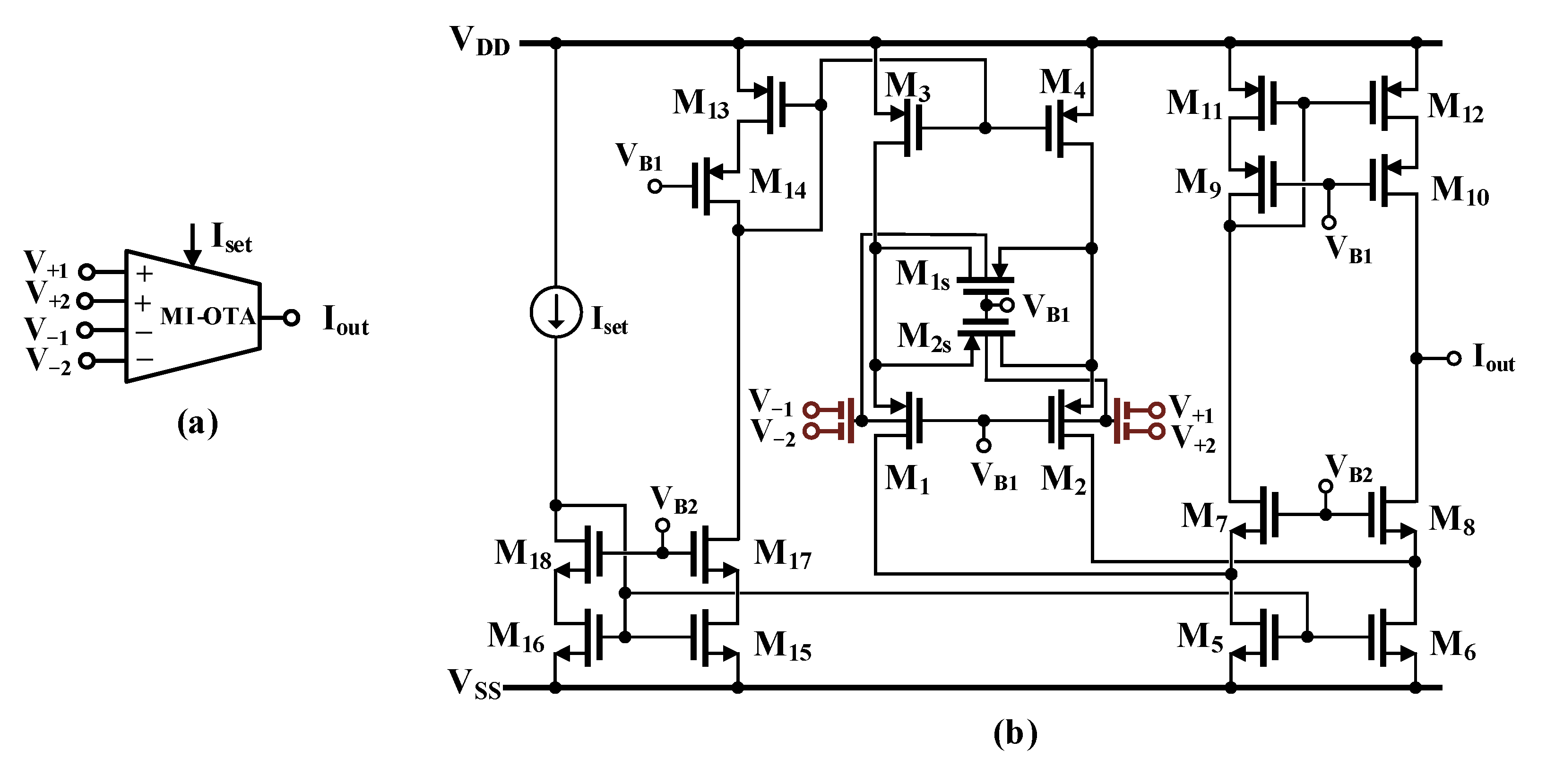
The symbol and the CMOS realization of the multiple-input OTA proposed in this work are shown in Figure 1a and 1b, respectively. The output current Iout can be described by the following equation:
where gm is the small-signal transconductance.
Overall, the circuit can be considered as a folded cascode OTA, with the input bulk-driven differential pair M1, M2 linearized using the triode region transistors M1s and M2s. A similar linearization technique was proposed by Krummenacher and Joehl [50] for a gate-driven transconductor operating in the strong inversion region. Figure 1 presents a BD counterpart of the circuit, operating in weak inversion, and with the input transistors replaced by multiple-input devices. Such a version of the input stage was first proposed and verified experimentally in [49].
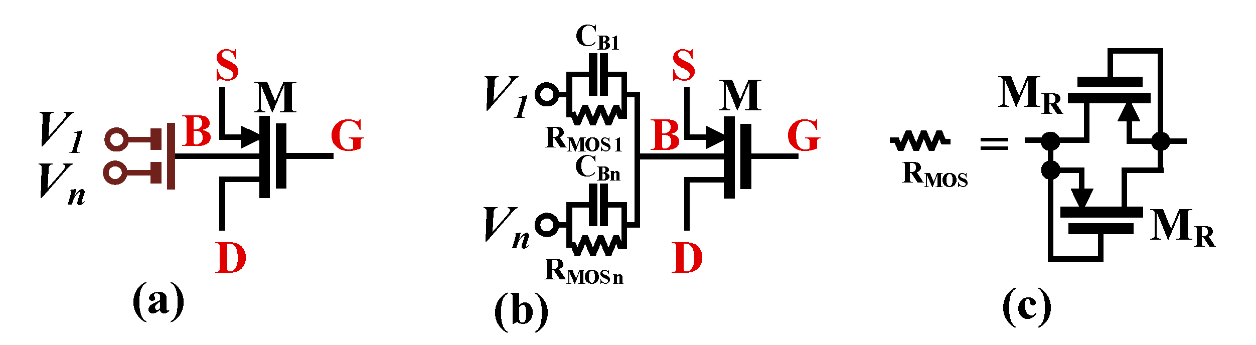
The practical realization of multiple-input devices is shown in Figure 2. Note that multiple inputs were realized using a capacitive voltage divider/analog summer, composed of the capacitors CBi. The large resistors RMOSi, connected in parallel to the capacitors, are used to properly bias the bulk terminal of the transistor for DC. They are realized as an anti-parallel connection of two minimum-size MOS transistors operating in the cut-off region. Due to their high resistances, their impact on the voltage transfer function of the input divider can be neglected for working frequencies of ω > 1/CBiRMOSi. In such a case, the AC voltage at the bulk terminal of the device can be expressed as follows:
where n is the number of inputs and βi is the voltage gain of the input capacitive divider from ith input. Neglecting second-order effects, βi can be expressed as follows:
Note that with identical CBi, βi = 1/n for i = 1, …, n.
Figure 2.
MIBD-MOST technique (a) symbol, (b) realization, and (c) RMOS realization.

The MOS transistor with a capacitive input divider can be seen as a new active device called a bulk-driven multiple-input MOS transistor [48]. The use of such devices enables the realization of input signal summation (see Equation (1)) without the need for a second input stage, thus simplifying the overall structure and saving dissipated power.
Regarding the input stage of the OTA, its linearity depends on the parameter k, which is defined as follows:
The best linearity of the input stage is achieved for k = 0.5 [49], i.e., the same value as for its GD counterpart operating in weak inversion [51]. This result does not depend on the value of the biasing current Iset if the operation in weak inversion is provided.
The rest of the OTA structure is rather conventional, with its cascode output stage M5-M12. The transistors M13-M18 are used for biasing purposes. All the transistors in the OTA circuit, except M1s and M2s, should operate in the penthode region.
The small-signal transconductance of the OTA can be expressed as follows [49]:
where η = gmb1,2/gm1,2 is the bulk-to-gate transconductance ratio of the input pair at the operating point, np is the subthreshold slope factor for p-channel devices, UT is the thermal potential, and the other symbols are explained earlier.
As can be concluded from (5), the resulting transconductance is attenuated by the input capacitive divider and by the application of bulk-driven devices (note that both the capacitive divider gain β and the bulk-to-gate transconductance ratio η are less than unity). The transconductance is proportional to the biasing current Iset, and thus can be linearly regulated by this current.
The relatively low value of the overall transconductance also decreases the voltage gain of the OTA. However, thanks to the high-resistance cascode output stage, the DC voltage gain of the OTA is maintained at a sufficient level as follows:
The input capacitive divider, as well as the bulk-driven technique, extend the linear range of the OTA 1/(βη) times. However, the input-referred noise is increased in the same proportion; thus, the dynamic range of the circuit remains unchanged as compared to its GD counterpart. Nevertheless, application of the bulk-driven technique, combined with an additional capacitive divider, simplifies the design of analog blocks in an ultra-low-voltage environment and avoids hard nonlinearities for a relatively large input voltage swing.
2.2. Proposed Electronically Tunable Current Conveyors
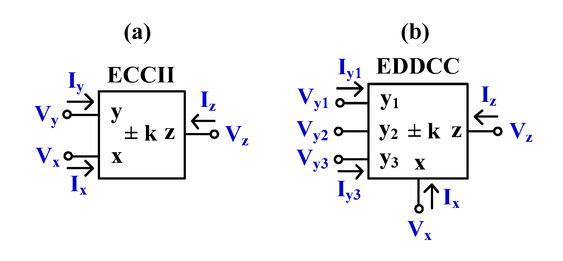
Figure 3a shows the symbol of the electronically tunable second-generation current conveyor (ECCII) and Figure 3b shows the electrical symbol of the electronically tunable differential difference current conveyor (EDDCC). The port characteristics of the ECCII and EDDCC can be expressed, respectively, as follows:
The characteristics of the ECCII and EDDCC are similar to the conventional CCII [2] and DDCC [14], except for the current gain between the x- and z-terminals, which can be given by k.
Figure 3.
The symbol of electronically tunable current conveyors (a) ECCII and (b) EDDCC.

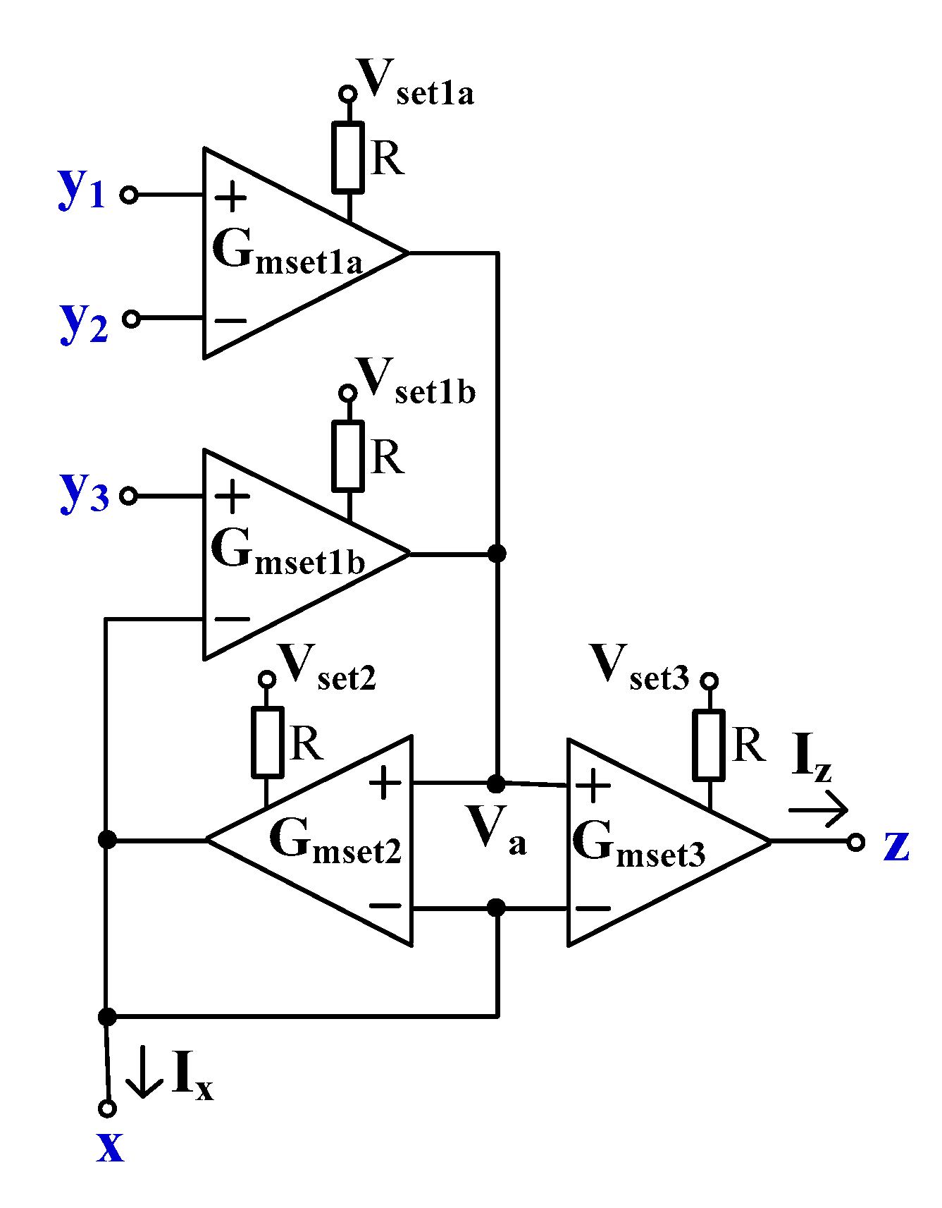
Figure 4 shows the proposed EDDCC using MI-OTAs. This circuit can also work as an ECCII if the y1-terminal is the input and the y2- and y3-terminals are connected to ground. It can further work as an inverting ECCII if the y2-terminal is the input and the y1- and y3-terminals are connected to ground.
To explain the operation of the proposed EDDCC, it is assumed that all OTAs are identical. Using (1), the currents I1, I2, and I3 in Figure 4 can be expressed as follows:
The OTA2 of Gmset2 is connected as a negative-feedback-like voltage follower (VF) circuit. Thus, Va = Vx and this voltage (i.e., Va = Vx) is fed to the inverting input terminal of OTA1 (Gmset1). Therefore, this OTA1 is also operated as a VF. The voltage relationship of the EDDCC in Figure 4 can be given as follows:
The addition and subtraction voltage properties of the EDDCC can be obtained.
By substituting (10) into (11), the relationship of the currents and can be expressed as follows:
Thus, the current gain of EDDCC can be varied by adjusting the ratio of Gmset3/Gmset2 (Gmset3/Gmset2 = k).
3. Applications of the EDDCC
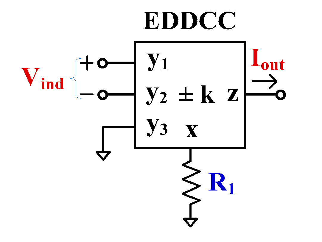
3.1. V-to-I Converter Using EDDCC
Voltage-to-current (V-to-I) converters, the so-called transconductors, are useful basic building blocks for realizing analog filters, oscillators, gyrators, and instrumentation amplifiers; for examples see [52,53,54,55,56]. In this work, the proposed EDDCC has been used to realize the V-to-I converter as shown in Figure 5. The voltage input () is converted to the output current () by R1 and the current gain can also be adjusted by the current gain k of the EDDCC. The circuit can work as a single-ended V-to-I converter (non-inverting or inverting input) and a differential V-to-I converter. Using (8), the output current of the circuit in Figure 5 can be expressed as follows:
where and .
3.2. Current-Mode Universal Filter Using EDDCCs
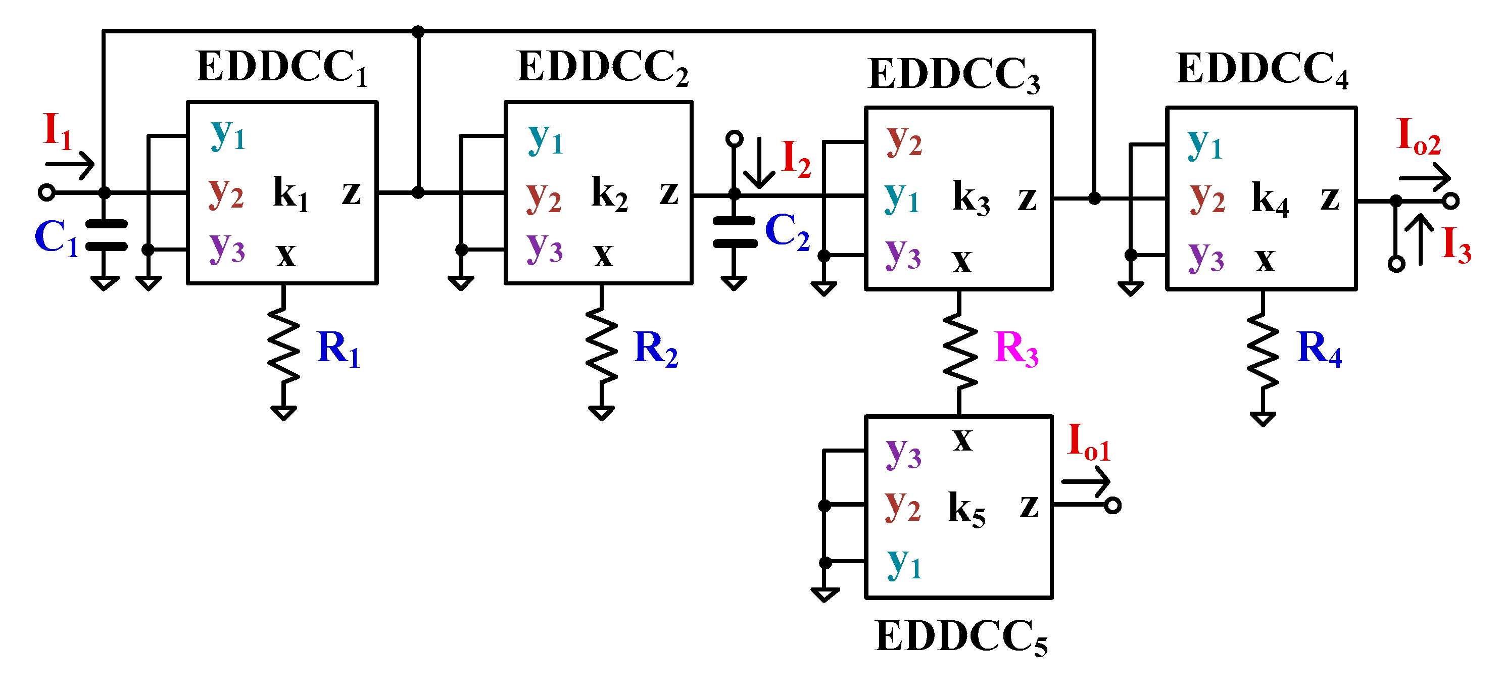
To show the advantages of the current gain of the EDDCC, the EDDCC has been used to realize a current-mode universal filter as shown in Figure 6. The filter employs five EDDCCs, four resistors, and two capacitors. The output terminals possess a high impedance level, and the circuit uses grounded capacitors, which is convenient for the implementation of integrated circuits. The filtering functions can be achieved through the appropriate use of input signals and appropriate selection of output signals.
Using (8) and nodal analysis, the output currents Io1 and Io2 can be expressed as follows:
where .
The variants of the current-mode universal filter’s filtering functions are shown in Table 1. The proposed filter offers five standard filtering functions. Moreover, the current gains of LP and BP filters can be adjusted by k4 and k5 of EDDCC4 and EDDCC5.
The natural frequency () and quality factor () can be expressed as follows:
The natural frequency can be given by RT and R3 (i.e., RT = R3) and the quality factor can be controlled independently and electronically by k1 of EDDCC1. The current gains of LP outputs Io1 and Io2 can be controlled by k5 and k4, respectively. In the case of tuning Q of the BP, the current gain will be equal to 1 if k1 = k4 for output Io2 or k1 = k5 for output Io1. The current gain of BP can be obtained if k4 > k1 (or k5 > k1).
3.3. Non-Ideal Analysis
Taking into account the non-idealities of the EDDCC, the relationship of the terminal voltages and currents can be rewritten as follows:
where αj1 = 1 − εj1v and εj1v (|εk1v| « 1) denotes the voltage-tracking error from Vy1 to Vx of the jth EDDCC, αj2 = 1 − εj2v and εj2v (|εj2v| « 1) denotes the voltage-tracking error from Vy2 to Vx of the jth EDDCC, αj3 = 1 − εj3v and εj3v (|εj3v| « 1) denotes the voltage-tracking error from Vy3 to Vx of the jth EDDCC, and βj = 1 − εi and εi (εi « 1) denotes the output current-tracking error of the jth EDDCC.
Using (20), the denominator of the proposed filter becomes as follows:
The natural frequency and quality factor become as follows:
It follows from (22) and (23) that tracking errors change the natural frequency and the quality factor. However, it should be noted that the natural frequency can be easily compensated by adjusting k2 and k3 and the quality factor can be compensated by adjusting k1.
With respect to the parasitic parameters of the EDDCC on the current-mode universal filter, the parasitic impedances Rz and Cz at the z-terminal [5] are considered. From Figure 6, it can be seen that capacitor C1 is in parallel with parasitic capacitances Cz1, Cz3 and parasitic resistances Rz1, Rz3 while capacitor C2 is in parallel with parasitic capacitance Cz2 and parasitic resistances Rz2. The parasitic effects on the pole frequency of the filter can be avoided by choosing C1 Cz1 + Cz3, C2 Cz2, R1 Rz1//Rz3, and R2 Rz2.
4. Simulation Results
The proposed EDDCC and its applications were simulated in the Cadence Virtuoso System Design Platform using 0.18µm CMOS technology from TSMC (Taiwan Semiconductor Manufacturing Company, Hsinchu Science Park, Taiwan). The aspect ratios of all MOS transistors of the MI-OTA in Figure 1 are listed in Table 2. The initial values of Iset1 = Iset2 = 5 μA, while the values of Iset3 were changed to adjust the current gain k of the EDDCC.
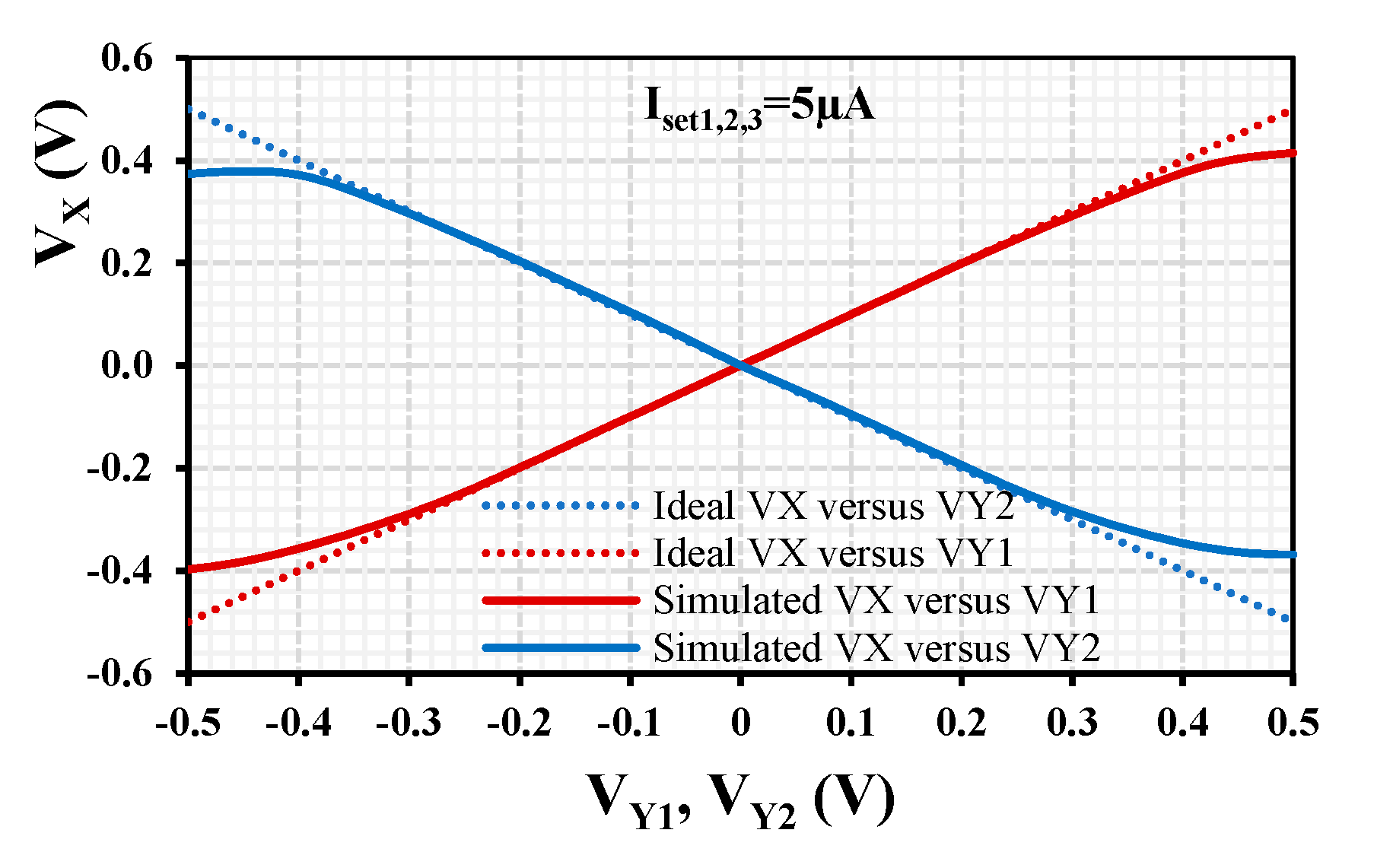
For the EDDCC in Figure 3b, the supply voltage was chosen to be VDD = –VSS = 0.5 V, with the setting currents Iset1 = Iset2 = Iset3 = 5 μA. The power consumption of the EDDCC was 90 μW. Figure 7, Figure 8, Figure 9, Figure 10, Figure 11 and Figure 12 show the simulation results of the EDDCC. Figure 7 shows the ideal and simulated DC voltage characteristics Vx versus Vy1 (Vy2 and Vy3 are grounded) and Vx versus Vy2 (Vy1 and Vy3 are grounded) when Vy1 and Vy2 were swept from −0.5 V to 0.5 V. A good linearity is evident for VX/VY1 and VX/VY2 with the input voltage range ±0.3 V.
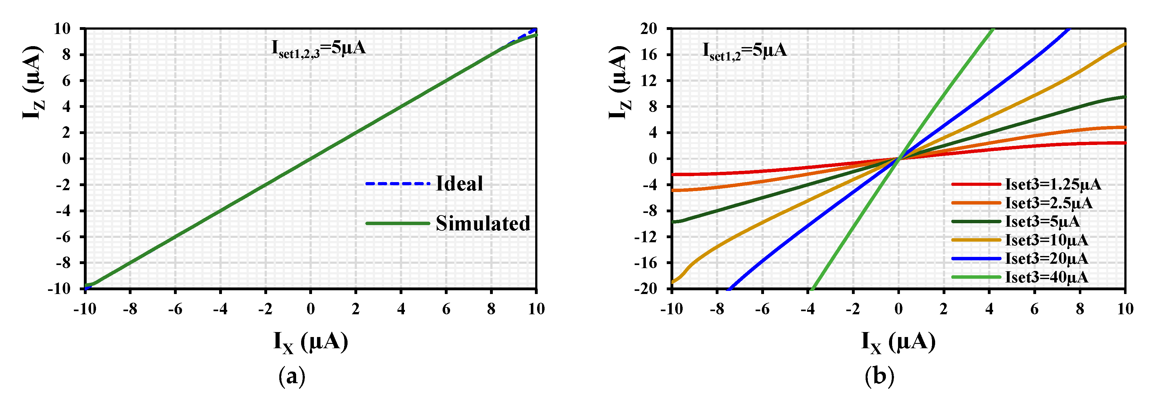
Figure 8a shows the ideal and simulated DC current characteristics Iz versus Ix (with k = 1) when IX was swept from −10 µA to +10 µA. The curves overlap in the range of ±9 µA. Figure 8b shows the Iz versus Ix for different k with a constant Iset1,2= 5 µA and varied Iset3= (1.25, 2.5, 5, 10, 20, 40) µA. The wide turnability of Iz versus Ix is evident.
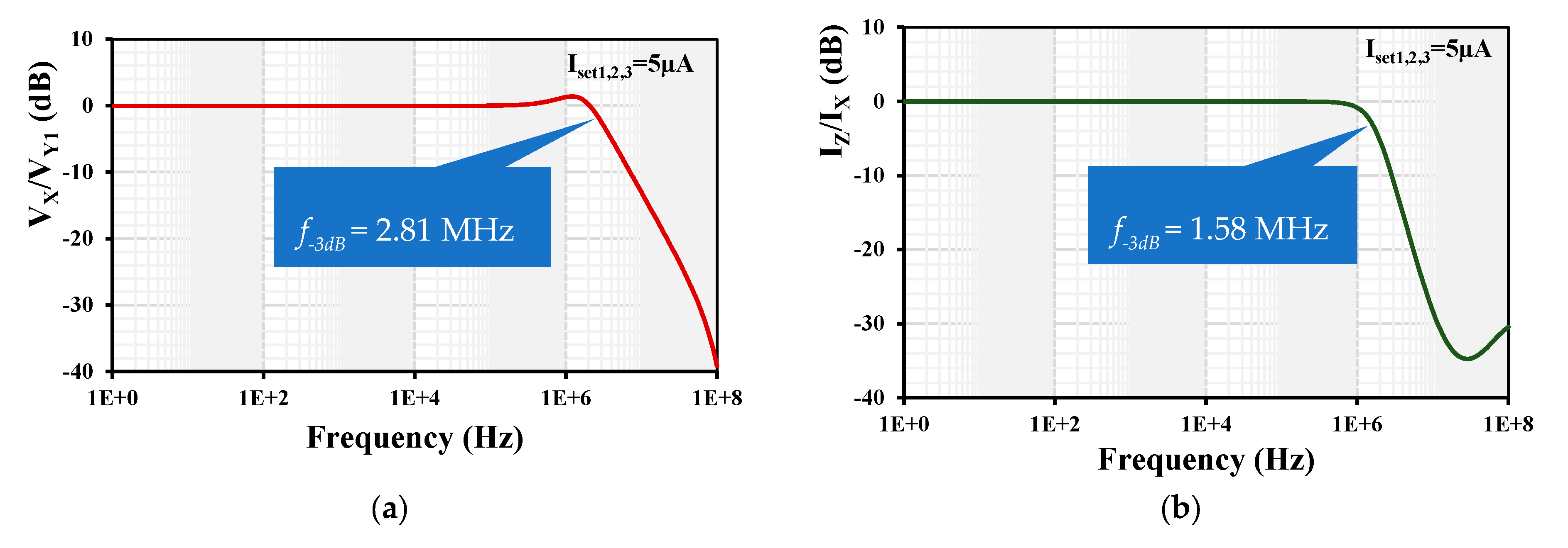
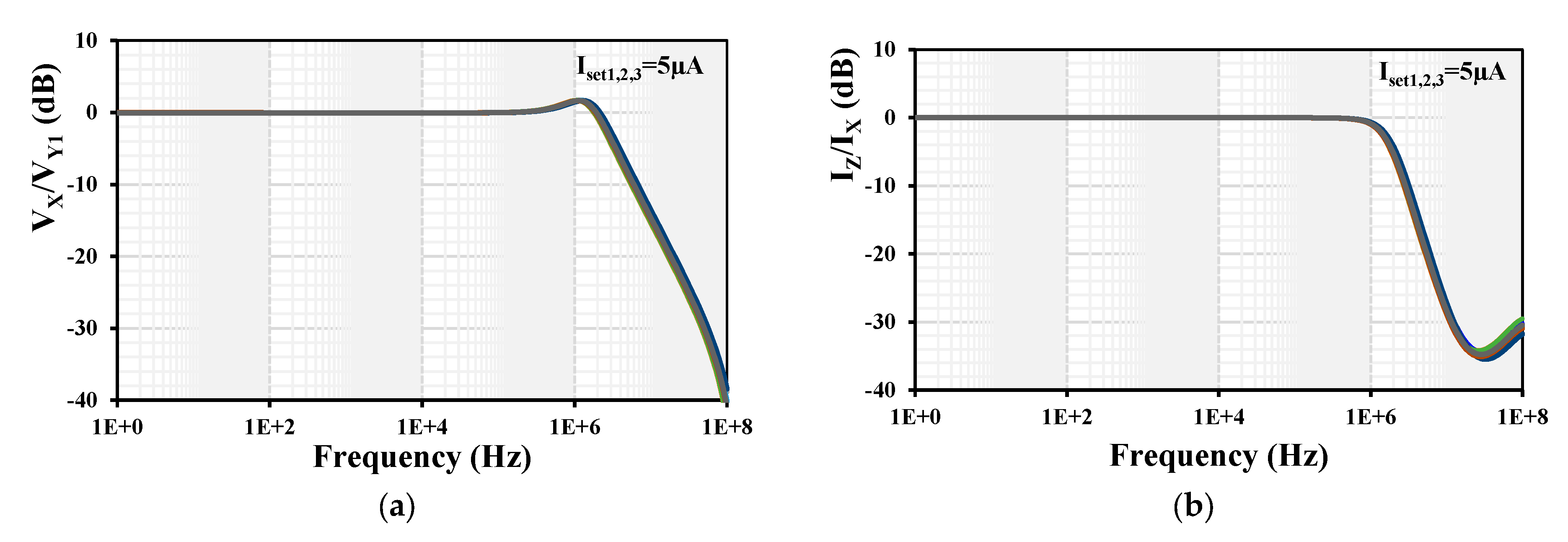
The simulated frequency responses of the voltage gain Vx/Vy1 and the current gain Iz/Ix are shown in Figure 9. The −3 dB bandwidths were 2.81 MHz and 1.58 MHz, and the low-frequency gains were −33.6 mdB and −76 µdB for the voltage Vx/Vy1 and current Iz/Ix gains, respectively. It is worth noting here that a compensation capacitor of 2 pF was connected between the input of Gmset2 to obtain a flat magnitude response of the current gain. Without this compensation capacitor, the peak is around 6 dB.
Process, voltage, temperature (PVT) corners were used to confirm the robustness of the design. The process transistor corners were fast-fast, fast-slow, slow-fast, and slow-slow; the process MIM capacitor corners were fast-fast and slow-slow; the voltage supply corners were = ±10% (VDD-VSS); and the temperature corners were −20 °C and 60 °C. The results for the frequency responses of the voltage gain Vx/Vy1 and current gain Iz/Ix are shown in Figure 10. The −3 dB bandwidths were in range of (2.66 to 3) MHz and (1.49 to 1.72) MHz, and the low-frequency gains were in range of (−62.8 to 21.2) mdB and (−124.6 to 79.9) µdB for the voltage Vx/Vy1 and current Iz/Ix gains, respectively. As is evident, the variations are within the acceptable range.
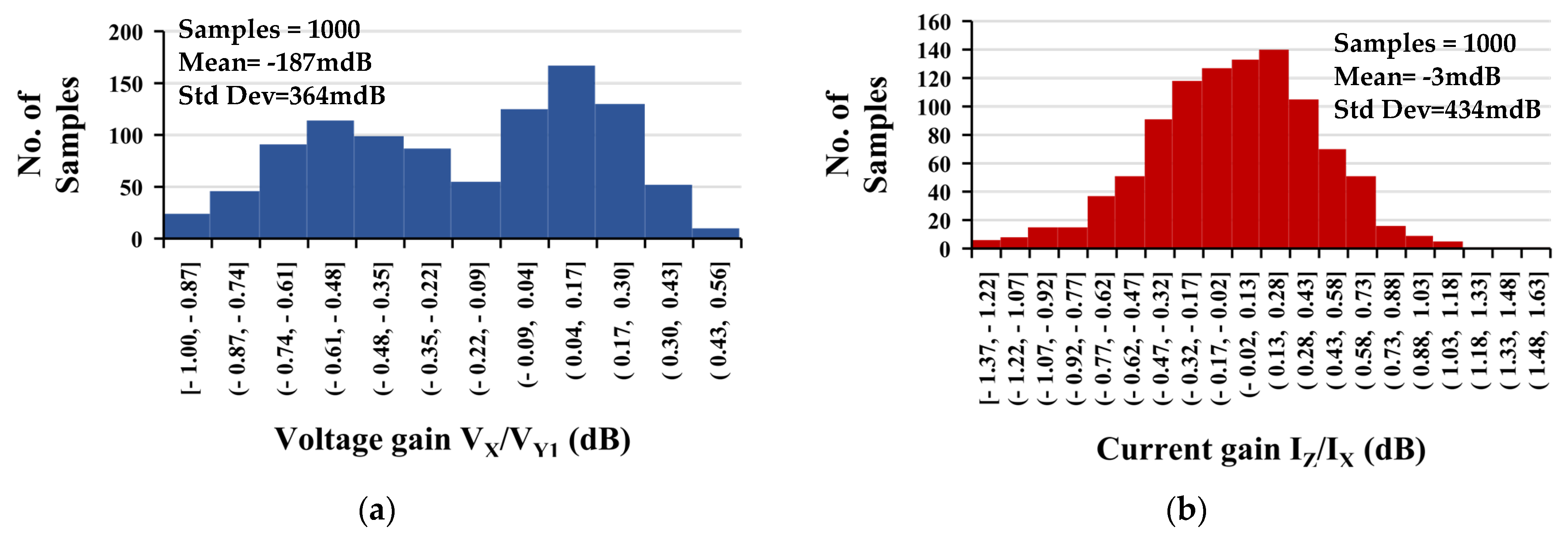
Monte Carlo (MC) analysis was used to perform the statistical analysis to estimate parametric yield and generate information about the performance characteristic of the frequency voltage gain Vx/Vy1 and current gain Iz/Ix of the EDDCC. Figure 11 shows the histogram of a 1000 run MC analysis, showing the mean value to be −187 mdB and −3 mdB, and the standard deviation to be 364 mdB and 434 mdB for the voltage and current gains, respectively.
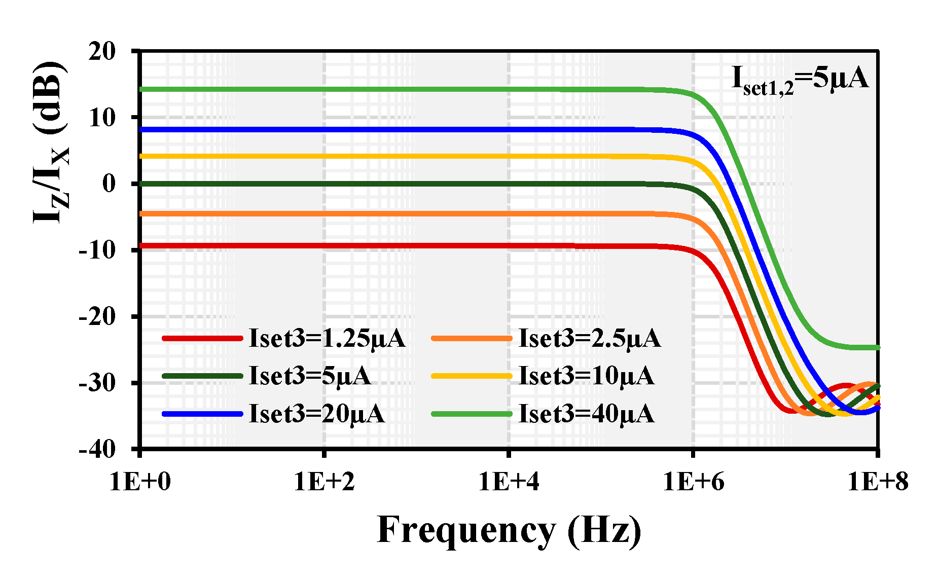
The simulated frequency response of the current gain Iz/Ix with a constant Iset1,2 = 5 µA and varied Iset3= (1.25, 2.5, 5, 10, 20, 40) µA is shown in Figure 12. The simulated current gain k was varied to (−9.3, −4.48, 0, 4.13, 8.1, 14.22) dB, respectively. This result confirms that the proposed EDDCC can provide the current gain Iz/Ix.
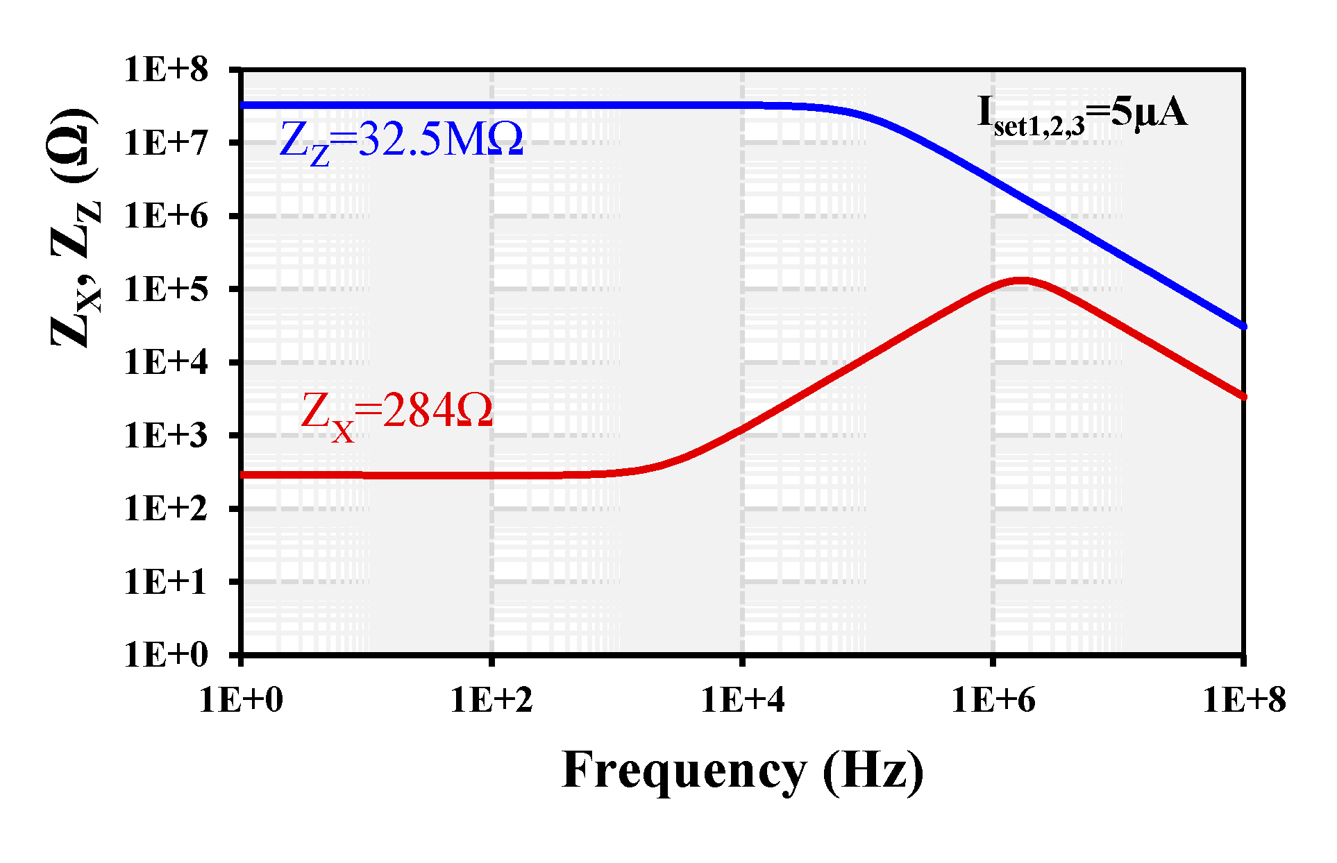
The simulated frequency dependence of the parasitic impedances of the z- and x-terminals is shown in Figure 13. The resistance of the z-terminal is 32.5 MΩ and the resistance of the x-terminal is 284 Ω for Iset1,2,3 = 5 µA.
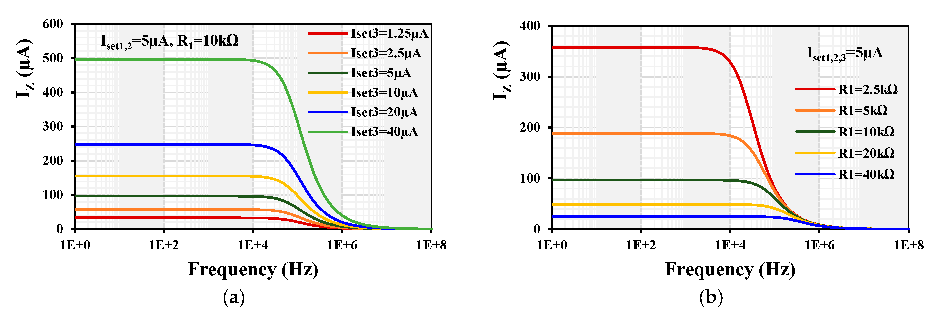
Figure 14a shows the frequency responses of the V-to-I converter shown in Figure 5 against the current gain k for a constant R1 = 10 kΩ, Iset1,2 = 5 µA, and various Iset3= (1.25, 2.5, 5, 10, 20, 40) µA, and Figure 14b for Iset1,2,3 = 5 µA and various R1 = (2.5, 5, 10, 20, 40) kΩ. The wide tunability of the current gain is evident.
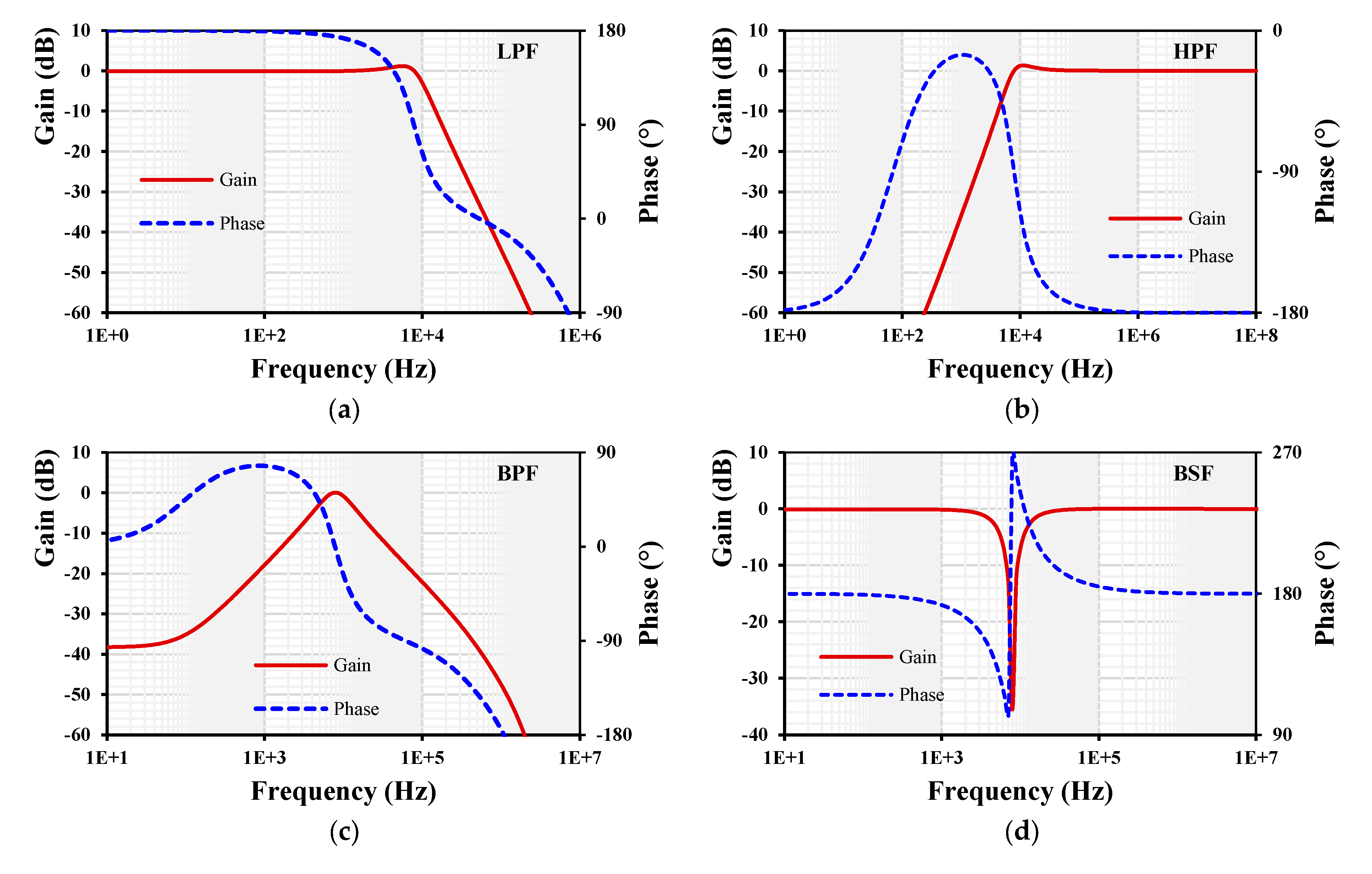
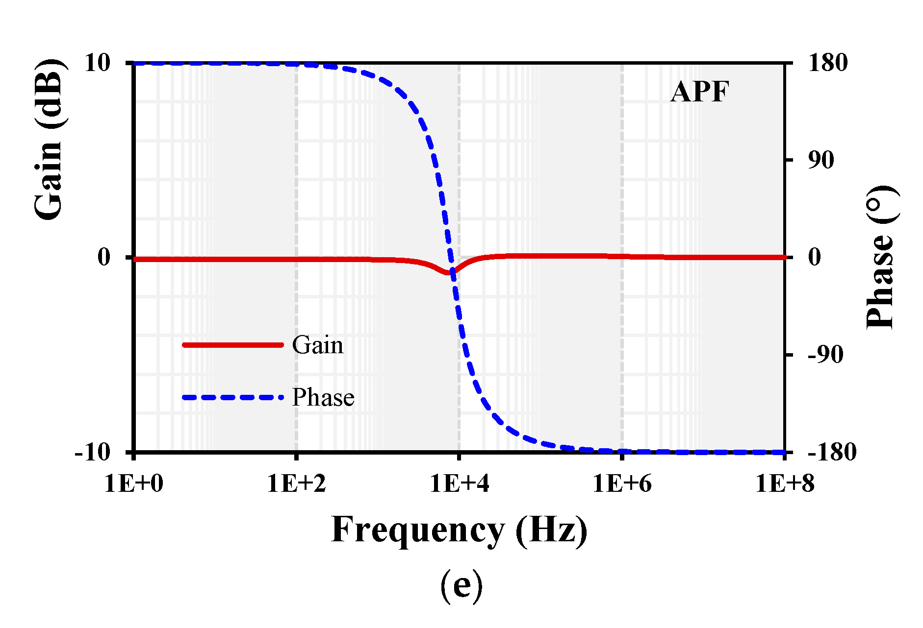
For simulation of the current-mode universal filter shown in Figure 6, the parameters C1 = C2 = 100 pF and R1–4 = 200 kΩ were chosen. The gain k1–5 = 1 was set by choosing the setting current of all EDDCC1–5 to be Iset = 5 µA. However, for the APF, the current of the EDDCC4 was set to Iset3 = 13 µA in order to obtain k = 2. The gain and phase frequency characteristics are shown in Figure 15. The cut-off frequency was 7.9 kHz.
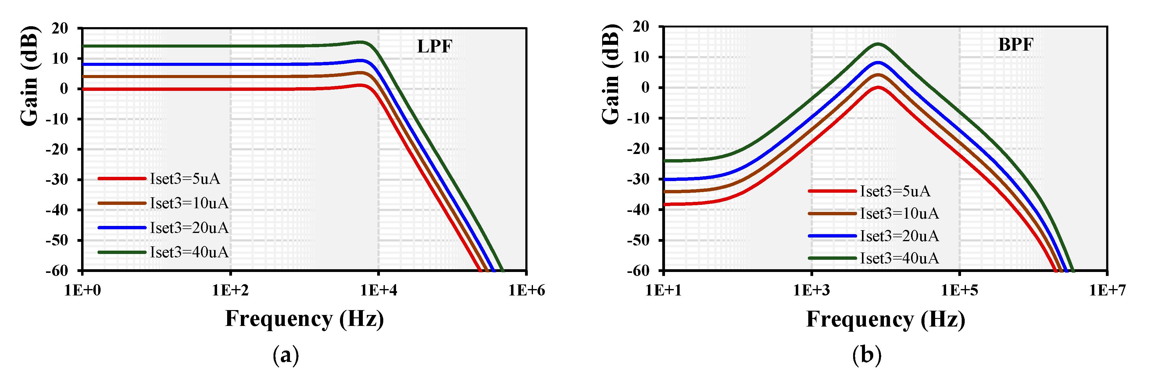
Figure 16 shows the tuning capability of the gain for the LPF and BPF. The setting current of all EDDCC1-4 was set to be Iset = 5 µA while the k of EDDCC5 was changed by its Iset3 = (5, 10, 20, 40) µA. The low-frequency gain of the LPF was around (0.1, 4, 8, 14) dB and for BPF, it was (0.02, 4.1, 8.1, 14.2) dB.
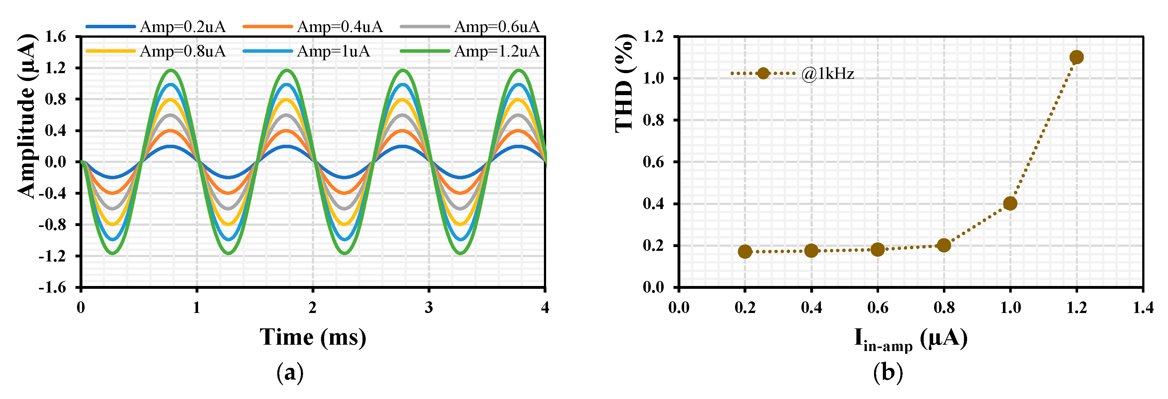
Figure 17 shows the transient response of the LPF’s output (a) and the total harmonic distortion (b) when an input signal at 1 kHz and different amplitudes (0.2, 0.4, 0.6, 0.8, 1, 1.2) µA were applied to the input of the filter. The gain was set to be k = 1. The THD of the output signal was below 1.2% for an input amplitude of 1.2 µA.
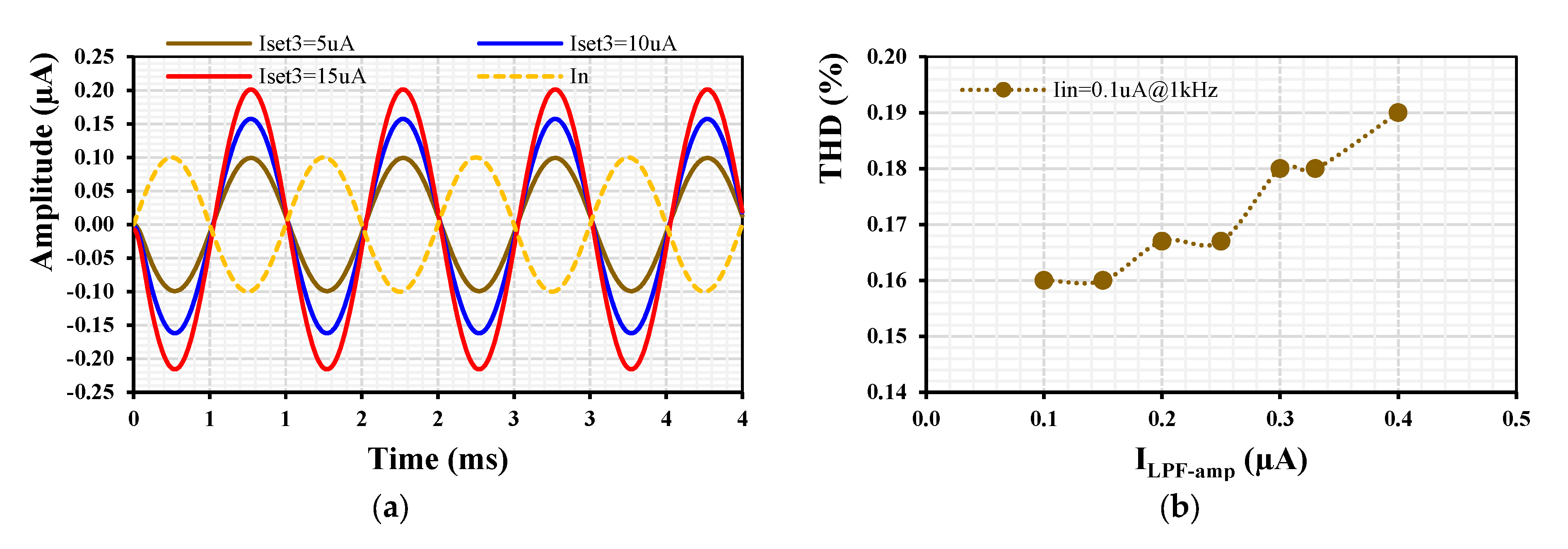
Figure 18a shows the transient response of the LPF when a sine wave Iin = 0.1 µA@1kHz is applied to the input of the filter with k1-4 = 1 (Iset = 5 µA) while the gain k5 of the EDDCC5 is varied by its Iset3 = (0.5, 10, 15) µA. The output signal of the LPF is inverted and amplified as expected. The THD is shown in Figure 18b, where the 0.19% THD is shown for a 0.4 µA amplitude output signal.
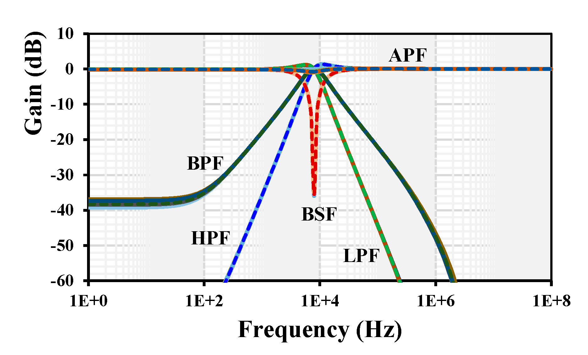
The PVT corners analysis was also used to confirm the robustness of the filter design. The results for the gains frequency responses of the LPF, HPF, BPF, BSF, and APF with PVT are shown in Figure 19. The curves of each filter response overlap, which confirms the robustness of the filter design.
The proposed EDDCC was compared with previous current conveyors in [18,21,23,33,41], as shown in Table 3. Current conveyors using nonconventional techniques, i.e., the bulk-driven CCII [18], bulk-driven DDCC [21], floating-gate FDCCII [23], and current conveyors providing current gain [33,41] have been selected for comparison. Compared with the current conveyors in [18,21,23], the proposed EDDCC offers current gain between z- and x-terminals. Compared with the ECCIIs in [33,41], the proposed EDDCC has much lower power consumption and lower supply voltage. It is worth noting that the bandwidth of the proposed EDDCC is sufficient for many applications like sensors and biomedical systems.
5. Experimental Measurements
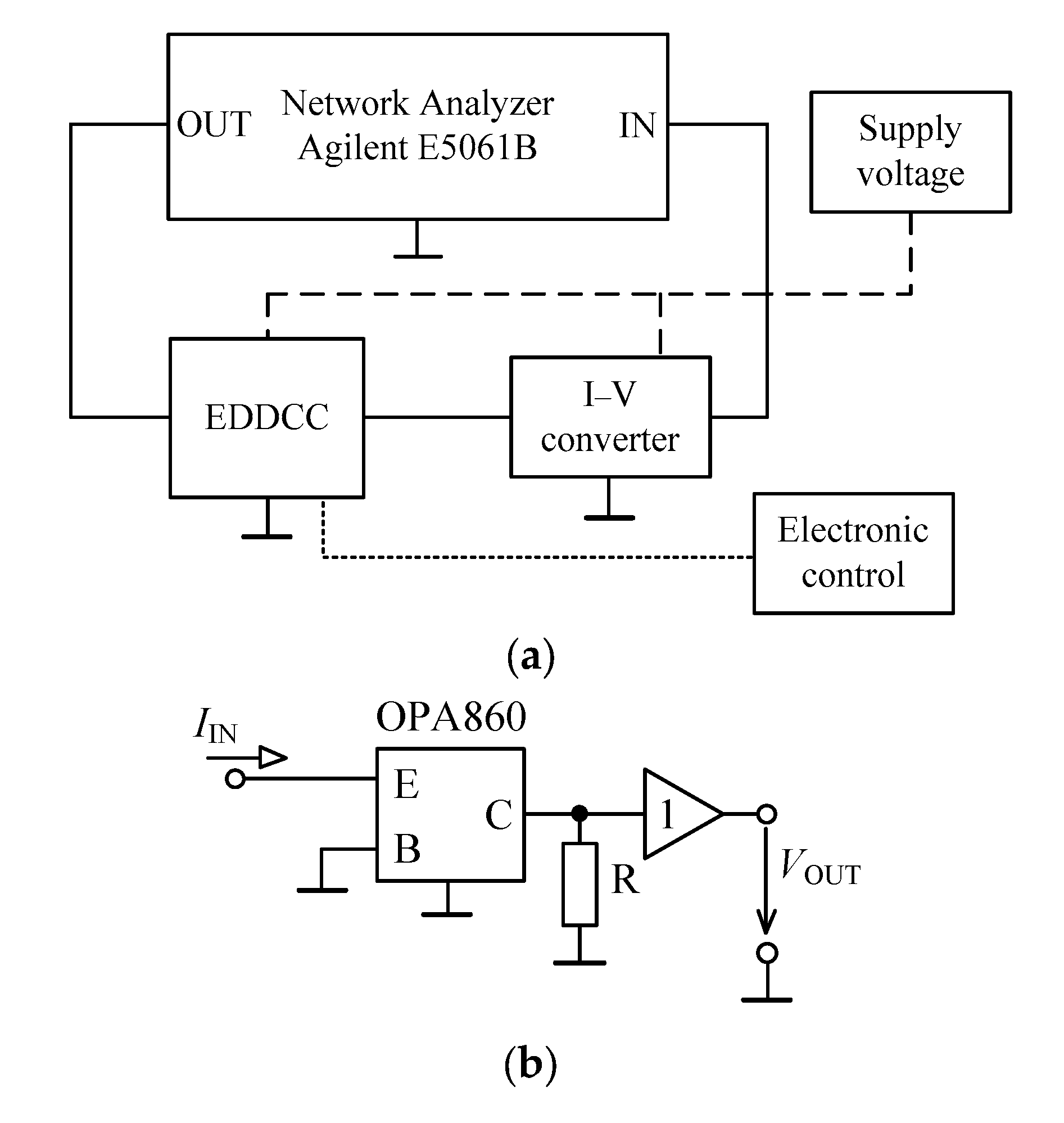
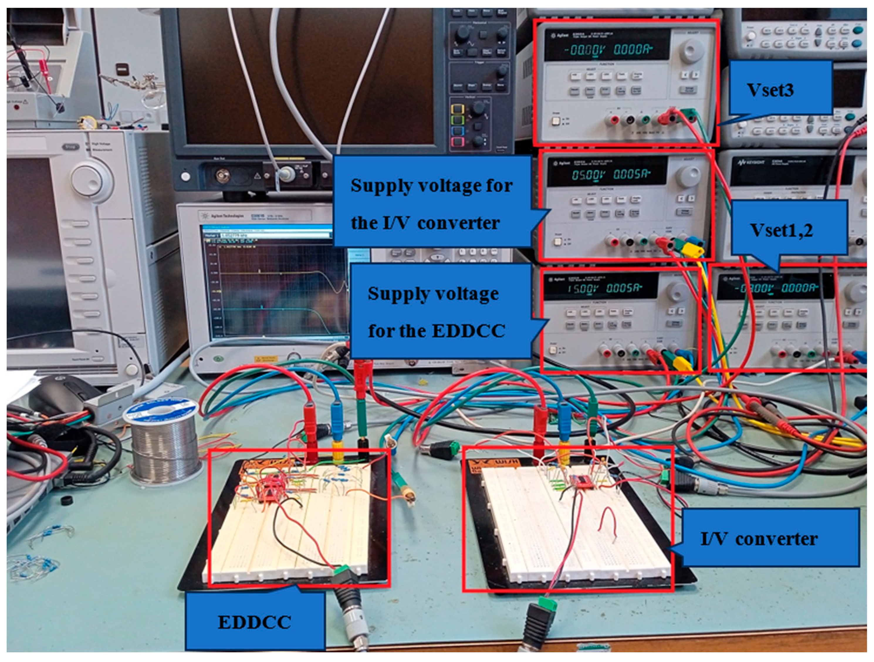
The proposed EDDCC was implemented using a commercially available LM13700 device (Texas Instruments, Dallas, TX, USA) [57]. The LM13700 IC uses a ± 15 V supply voltage and its transconductance is controlled by DC current. Since the EDDCC requires an OTA with four inputs (see Figure 4) and the LM13700 device has two inputs, the EDDCC has been implemented using four LM13700 (see Figure 20), where one provides inputs y1 and y2 and another provides input y3 (the positive input of the LM13700 is y3, while the negative input is connected to node x). Therefore, Gmset1 transfer has been divided into Gmset1a and Gmset1b while these transfers are set to an identical value, thus, Gmset1a = Gmset1b = Gmset1. The output currents of these two OTAs are then summed in node Va. The control of the transconductances of the LM13700 devices, in this particular implementation, is performed by the control DC voltage Vset (the control DC current setting transconductances is controlled by these voltages while the value of the resistor R is kept constant (32 kΩ)). The measurement has been performed using a network analyzer Agilent E5061B, generator Keysight 33500B, and oscilloscope Keysight CX3324A with a current probe CX1101A (Keysight, Santa Rosa, CA, USA). Figure 21a represents a block diagram of the used measurement setup while using the network analyzer. A simple I/V converter (shown in Figure 21b) based on a commercially available OPA860 IC (Texas Instruments) [58] has been used. Its function is as follows: the OPA860 serves as a current follower, the output current is transferred into voltage by the resistor R, and the node with the resistor R is separated from the converter output by a buffer (included in the OPA860 IC) for better impedance properties. The converter uses a supply voltage of ±5 V. A photo of the measuring workplace is depicted in Figure 22.
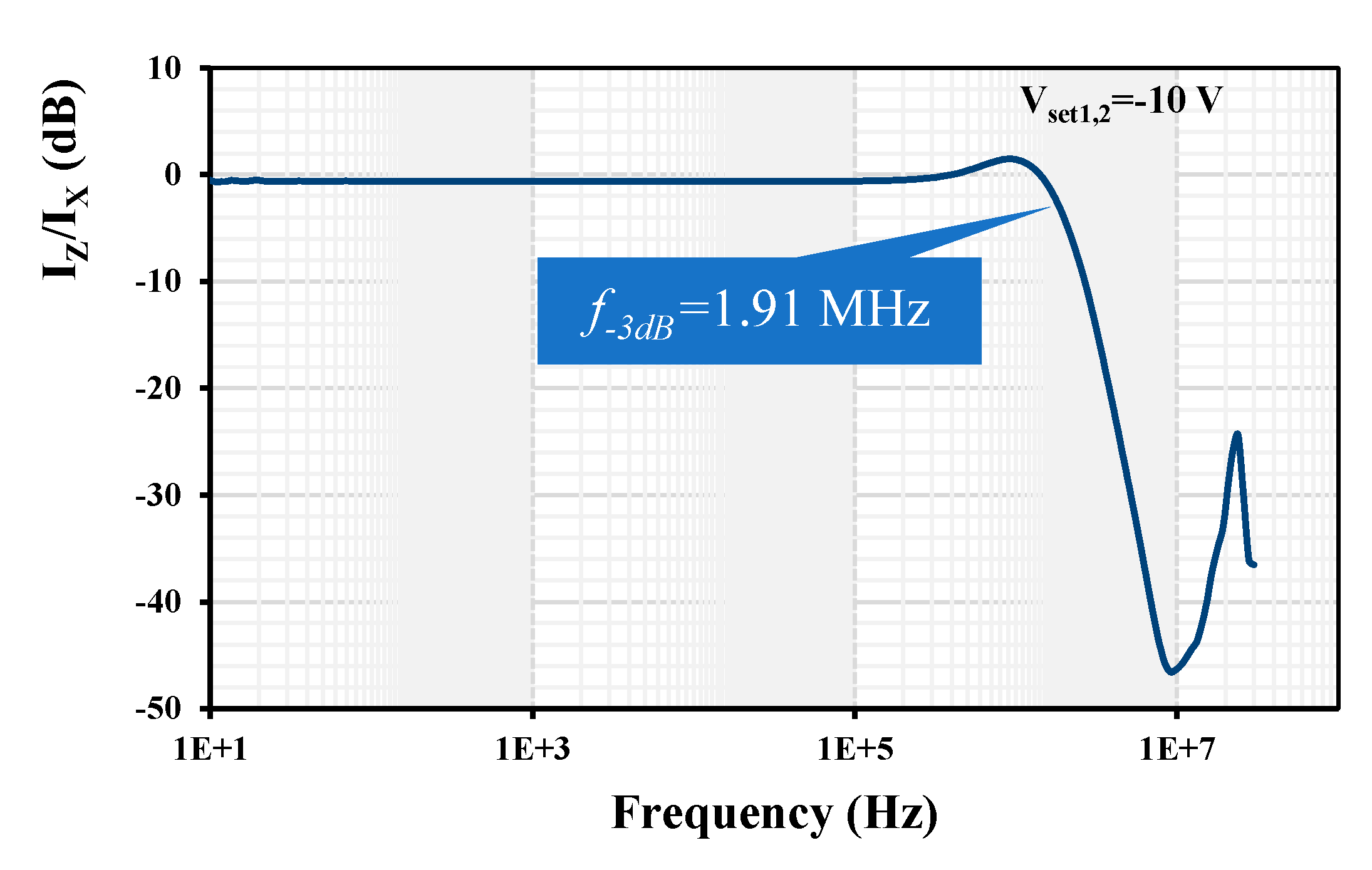
The default values for the measurement were selected as follows: Rx = 1 kΩ, Vset1 = Vset2 = −10 V, and Vset3 = 0 V. This way, the transconductance of the EDDCC is approximately 1 mS, corresponding to the resistor (1 kΩ) used in the I/V converter for the conversion of the current from the EDDCC back to voltage, which is then fed back to the network analyzer. Note that the resulting voltage transfer corresponds to Iz/Ix transfer when taking the transfer of the I/V converter as a constant. Figure 23 shows the measured current gain Iz/Ix for the default setting. The measurement has been performed in band from 10 Hz up to 30 MHz (the analyzer bandwidth range). The −3 dB bandwidth was measured at 1.91 MHz. The gain is −0.53 dB (note that the resulting gain is given by how accurately the transfer of the EDDCC compensates the transfer of the I/V converter).
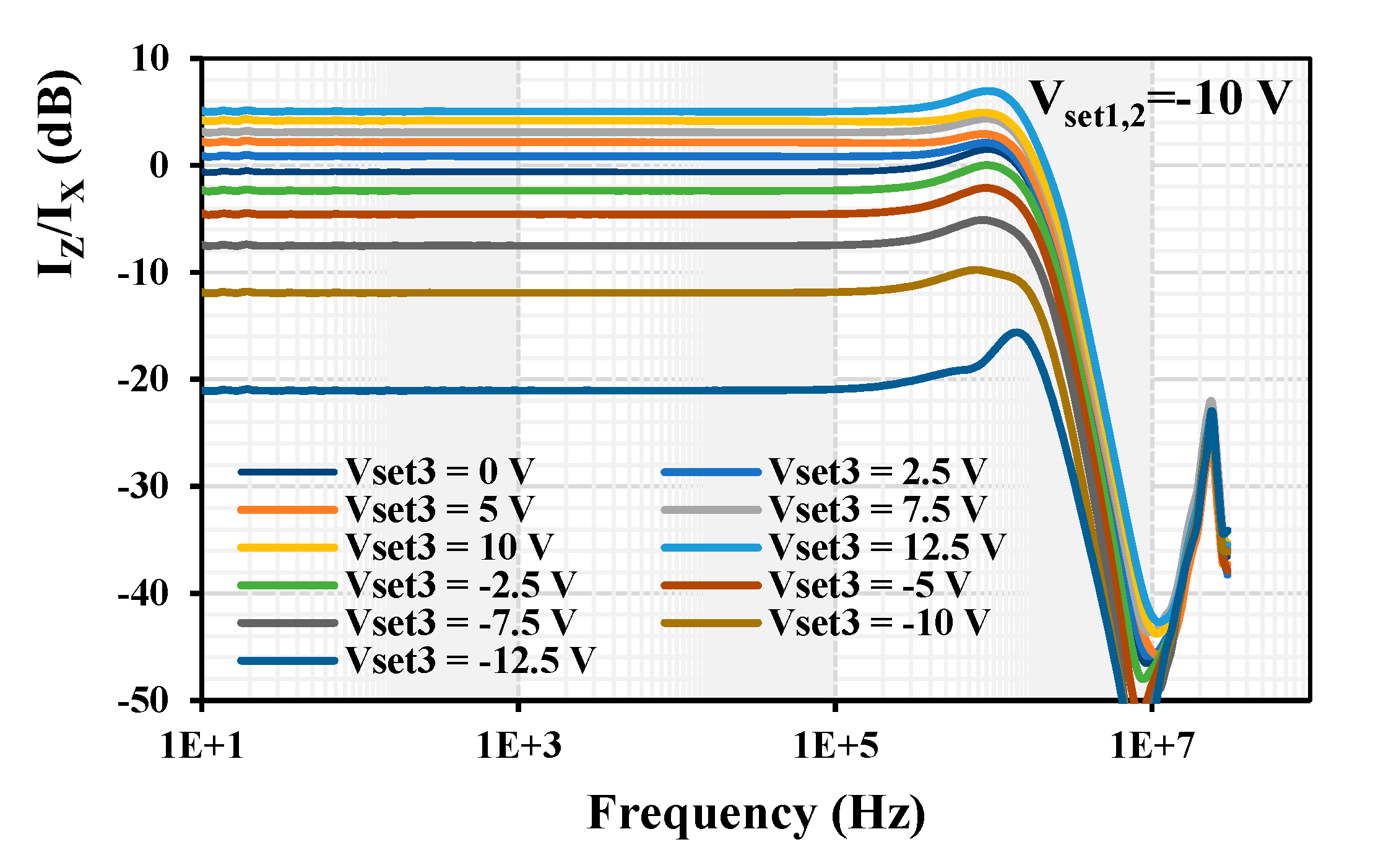
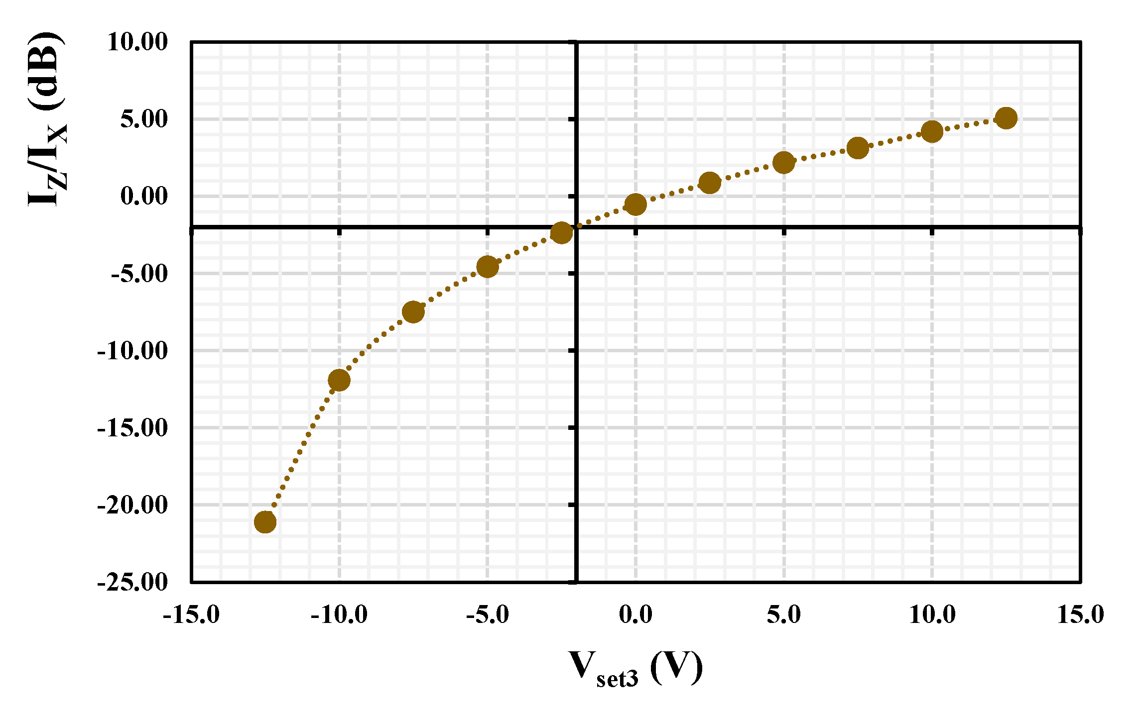
The possibility to change the current gain Iz/Ix by varying Vset3 = (−12.5, −10, −7.5, −5, −2.5, 0, 2.5, 5, 7.5, 10, 12.5) V is shown in Figure 24. The obtained current gain was (−21.11, −11.92, −7.50, −4.57, −2.37, −0.53, 0.86, 2.18, 3.11, 4,18, 5.05) dB, respectively. Figure 25 depicts the dependency of the current gain Iz/Ix on the control voltage Vset3. It shows a logarithmic dependency of the current gain on the control voltage based on this particular implementation.
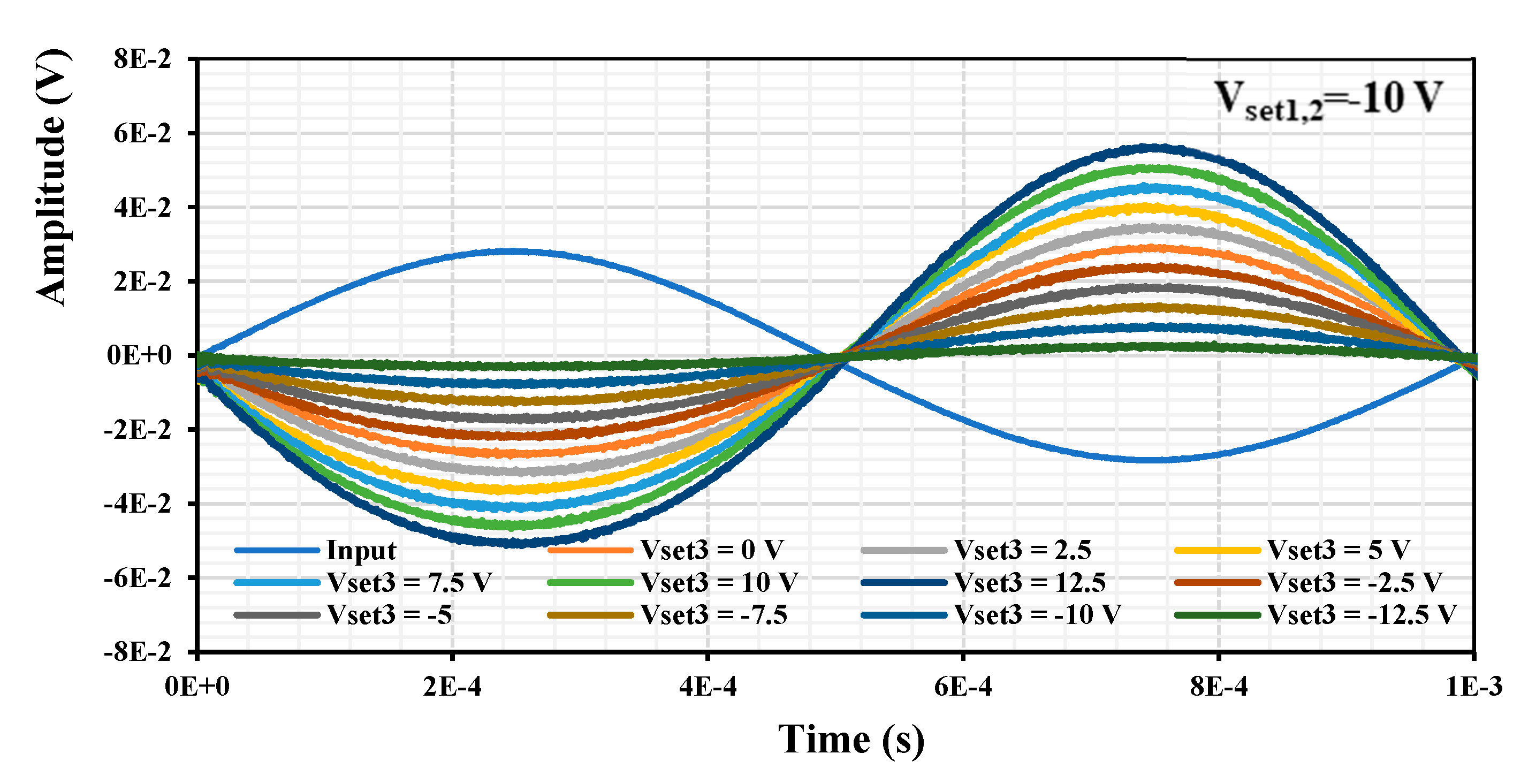
The measured time domain results of voltage-to-voltage transfer (input of the EDDCC and output of the I/V converter) are presented in Figure 26. The input signal measured at the input of the EDDCC had an amplitude of 57 mV and frequency of 1 kHz. The output signal for Vset3 = (−12.5, −10, −7.5, −5, −2.5, 0, 2.5, 5, 7.5, 10, 12.5) V is (6, 15, 26, 35, 44, 55, 66, 76, 85, 97, 107) mV, which provides the gain (−19.55, −11.60, −6.85, −4.24, −2.25, −0.31, 1.27, 2.50, 3.47, 4.62, 5.47) dB. There is a 180° of the output in comparison to the input given by the I/V converter (its transfer is inverting). These values correspond well with the values of the current gain Iz/Ix obtained by the analyzer.
6. Conclusions
In this paper, a new low-voltage low-power electronically tunable current conveyor has been proposed. Unlike previous current conveyors, the current gain of the proposed current conveyor can be controlled electronically. The proposed current conveyor can work as an electronically tunable DDCC (EDDCC) and an electronically tunable CCII (ECCII). To show the advantages of the current gain of the proposed current conveyors, the V-to-I converter and current-mode universal filter were presented, and the simulation results confirm the functionality of the proposed circuits. The proposed EDDCC uses ±0.5 V power supply, consumes 90 μW of power, and has a ±200 mV DC voltage range, ±10 μA DC current range, and 90 μV voltage offset. The proposed circuit can also offer a 2.81 MHz bandwidth of the voltage gain Vx/Vy, a 1.58 MHz bandwidth of the current gain Iz/Ix, and a current gain of −9.3 to 14.22 dB when the bias current is varied from 1.25 μA to 40 μA. In addition, the experimental measurements of the EDDCC further support the concept and its functionality.
Author Contributions
Conceptualization, M.K., F.K. and T.K.; methodology, M.K., F.K. and T.K.; software, M.K. and F.K; validation, M.K., F.K. and L.L.; formal analysis, M.K. and T.K.; investigation, M.K., F.K. and T.K.; resources, M.K.; data curation, M.K and F.K.; writing—original draft preparation, M.K., F.K., T.K. and L.L.; writing—review and editing, M.K., F.K., T.K. and L.L.; visualization, M.K. and F.K.; supervision, M.K. and F.K.; project administration, M.K. and F.K.; funding acquisition, M.K. All authors have read and agreed to the published version of the manuscript.
Funding
This work was supported in part by the School of Engineering, King Mongkut’s Institute of Technology Ladkrabang, under Grant KREF046505, and by the University of Defence within the Organization Development Project VAROPS.
Institutional Review Board Statement
Not applicable.
Informed Consent Statement
Not applicable.
Data Availability Statement
Data are contained within the manuscript.
Conflicts of Interest
The authors declare no conflicts of interest.
References
- Kennedy, E.J. Operational Amplifier Circuits: Theory and Applications; Holt, Rinehart, and Winston: Austin, TX, USA, 1988. [Google Scholar]
- Sedra, A.; Smith, K.C. A second-generation current conveyor and its applications. IEEE Trans. Circuit Theory 1970, 17, 132–134. [Google Scholar] [CrossRef]
- Soliman, A.M. Current-mode universal filters using current conveyors: Classification and review. Circuits Syst. Signal Process. 2008, 27, 405–427. [Google Scholar] [CrossRef]
- Yucel, F.; Yuce, E. Grounded capacitor based fully cascadable electronically tunable current-mode universal filter. AEU-Int. J. Electron. Commun. 2017, 79, 116–123. [Google Scholar] [CrossRef]
- Yucehan, T.; Yuce, E. CCII-based voltage-mode and current-mode high-order filters with gains and grounded passive elements only. AEU-Int. J. Electron. Commun. 2022, 155, 154346. [Google Scholar] [CrossRef]
- Signh, D.; Paul, S.K. Improved current mode biquadratic shadow universal filter. Inf. MIDEM 2022, 52, 51–66. [Google Scholar] [CrossRef]
- Soliman, A.M. New grounded-capacitor current-mode oscillators using single-output CCIIs. J. Circuits Syst. Comput. 1998, 8, 363–378. [Google Scholar] [CrossRef]
- Horng, J.-W. A sinusoidal oscillator using current-controlled conveyors. Int. J. Electron. 2001, 88, 659–664. [Google Scholar] [CrossRef]
- Soliman, A.M. Current mode CCII oscillators using grounded capacitors and resistors. Int. J. Circuit Theory Appl. 1998, 26, 431–438. [Google Scholar] [CrossRef]
- Bajer, J.; Lahiri, A.; Biolek, D. Current-mode CCII+ based oscillator circuits using a conventional and a modified Wien-bridge with all capacitors grounded. Radioengineering 2011, 20, 245–250. [Google Scholar]
- Koton, J.; Herencsar, N.; Vrba, K. Current and voltage conveyors in current- and voltage-mode precision full-wave rectifiers. Radioengineering 2011, 20, 19–24. [Google Scholar]
- Monpapassorn, A. Low output impedance dual CCII full-wave rectifier. Int. J. Electron. 2013, 100, 648–654. [Google Scholar] [CrossRef]
- Petrovic, P.B. Current/voltage mode full-wave rectifier based on a single CCCII. Int. J. Circuit Theory Appl. 2020, 48, 1140–1153. [Google Scholar] [CrossRef]
- Chiu, W.; Liu, S.-I.; Tsao, H.-W.; Chen, J.-J. CMOS differential difference current conveyors and their applications. IEE Proceeding Circuits Devices Syst. 1996, 143, 91–96. [Google Scholar] [CrossRef]
- Elwan, H.O.; Soliman, A.M. Novel CMOS differential voltage current conveyor and its application. IEE Proc.-Circuits Devices Syst. 1997, 144, 195–200. [Google Scholar] [CrossRef]
- El-Adawy, A.A.; Soliman, A.M.; Elwan, H.O. A novel fully differential current conveyor and applications for analog VLSI. IEEE Trans. Circuits Syst.-II 2000, 47, 306–313. [Google Scholar] [CrossRef]
- Alzaher, H.A.; Elwan, H.; Ismail, M. A CMOS fully balanced second-generation current conveyor. IEEE Trans. Circuits Syst. II Analog Digit. Signal Process. 2003, 50, 278–287. [Google Scholar] [CrossRef]
- Reda, A.; Ibrahim, M.F.; Farag, F. Input–output Rail-to-Rail CMOS CCII for low voltage–low power applications. Microelectron. J. 2016, 48, 60–75. [Google Scholar] [CrossRef]
- Stornelli, V.; Pantoli, L.; Ferri, G.; Liberati, L.; Centurelli, F.; Monsurrò, P. Trifiletti. The AB-CCII, a novel adaptive biasing LV-LP current conveyor architecture. AEU-Int. J. Electron. Commun. 2017, 79, 301–306. [Google Scholar] [CrossRef]
- El Beqal, A.; Benhala, B.; Zorkani, I. Design of low-voltage low-power CMOS second generation current conveyor by using the genetic algorithm. In Proceedings of the 2022 2nd International Conference on Innovative Research in Applied Science, Engineering and Technology (IRASET), Meknes, Morocco, 3–4 March 2022; pp. 1–5. [Google Scholar] [CrossRef]
- Khateb, F.; Kumngern, M.; Spyridon, V.; Psychalinos, C. Differential difference current conveyor using bulk-driven technique for ultra-low-voltage applications. Circuits Syst. Signal Process. 2014, 33, 159–176. [Google Scholar] [CrossRef]
- Kumngern, M.; Khateb, F.; Kulej, T. 0.3 V differential difference current conveyor using multiple-input bulk-driven technique. Circuits Syst. Signal Process. 2020, 39, 3189–3205. [Google Scholar] [CrossRef]
- Fani, R.; Farshidi, E. A FG-MOS based fully differential current controlled conveyor and its applications. Circuits Syst. Signal Process. 2013, 32, 993–1011. [Google Scholar] [CrossRef]
- Suwansawang, S.; Thongleam, T. A 1-V bulk-driven CMOS fully differential second-generation current conveyor. In Proceedings of the 2013 International Symposium on Intelligent Signal Processing and Communication Systems, Naha, Japan, 12–15 November 2013; pp. 662–665. [Google Scholar] [CrossRef]
- Veerendranath, P.S.; Singh, S. 0.5 V, 10.94 μW, 36.89 μVrms IRN, 3rd order bulk-driven quadrature filter using fully differential current conveyor for bluetooth applications. Analog Integr. Circuits Signal Process. 2021, 109, 57–67. [Google Scholar] [CrossRef]
- Chunhua, W.; Qiujing, Z.; Haiguang, L. CMOS current controlled fully balanced current conveyor. J. Semicond. 2009, 30, 075009. [Google Scholar] [CrossRef]
- Kumngern, M.; Khateb, F.; Kulej, T. Bulk-driven fully balanced second-generation current conveyor in 0.18 µm CMOS. AEU-Int. J. Electron. Commun. 2019, 104, 66–75. [Google Scholar] [CrossRef]
- Veerendranath, P.S.; Sharma, V.; Vasantha, M.H.; Kumar, Y.B.N. ±0.5 V, 254 μW second-order tunable biquad low-pass filter with 7.3 fJ FOM using a novel low-voltage fully balanced current-mode circuit. Circuits Syst. Signal Process. 2021, 40, 2114–2134. [Google Scholar] [CrossRef]
- Senani, R. Novel circuit implementation of current conveyors using an OA and an OTA. Electron. Lett. 1980, 16, 2–3. [Google Scholar] [CrossRef]
- Surakampontorn, W.; Thitimajshima, P. Integrable electronically tunable current conveyors. IEE Proc. G (Electron. Circuits Syst.) 1988, 135, 71–77. [Google Scholar] [CrossRef]
- Fabre, A.; Mimeche, N. Class A/AB second generation current conveyor with controlled current gain. Electron. Lett. 1996, 43, 82–91. [Google Scholar] [CrossRef]
- Surakampontorn, W.; Kumwachara, K. CMOS-based electronically tunable current conveyor. Electron. Lett. 1992, 28, 1316–1317. [Google Scholar] [CrossRef]
- Mimaei, S.; Sayin, O.K.; Kuntman, H. A New CMOS electronically tunable current conveyor and its application to current-mode filters. IEEE Trans. Circuits Syst.–I Regul. Pap. 2006, 53, 1448–1458. [Google Scholar] [CrossRef]
- Song, S.-X.; Xie, H.-G.; Huang, S.-L. A new CMOS electronically tunable current conveyor based on programmable current amplifier. In Proceedings of the 2011 International Conference on Electric Information and Control Engineering, Wuhan, China, 23–25 September 2011; pp. 1043–1046. [Google Scholar] [CrossRef]
- Yamacli, S.; Ozcan, S.; Kuntman, H. A novel active circuit building block: Electronically tunable differential difference current conveyor (EDDCC) and its application to KEN filter design. In Proceedings of the 2006 International Conference on Applied Electronics, Pilsen, Czech Republic, 6–7 September 2006; pp. 237–240. [Google Scholar] [CrossRef]
- Knobnob, B. Electronically tunable differential difference current conveyor using commercially available OTAS. J. Circuits Syst. Comput. 2023, 32, 2350295. [Google Scholar] [CrossRef]
- Altun, M.; Kuntman, H.; Minaei, S.; Sayin, O.K. Realisation of nth-order current transfer function employing ECCIIs and application examples. Int. J. Electron. 2009, 96, 1115–1126. [Google Scholar] [CrossRef]
- Jaroslav, K.; Norbert, H.; Oguzhan, C.; Kamil, V. Current-mode KHN equivalent frequency filter using ECCIIs. In Proceedings of the 33rd International Conference on Telecommunications and Signal Processing (TSP), Vienna, Austria, 17–20 August 2010; pp. 27–30. [Google Scholar]
- Hassan, T.M.; Mahmoud, S.A. Fully programmable universal filter with independent gain-ωo-Q control based on new digitally programmable CMOS CCII. J. Circuits Syst. Comput. 2009, 18, 875–897. [Google Scholar] [CrossRef]
- Sayin, O.K.; Kuntman, H.H. Design of high-order active filters employing CMOS ECCIIs. In Proceedings of the IEEE 12th Signal Processing and Communications Applications Conference, Kusadasi, Turkey, 30 April 2004; pp. 375–378. [Google Scholar] [CrossRef]
- Kumngern, M.; Wareechol, E.; Phasukkit, P. Quadrature oscillator and universal filter based on translinear current conveyors. AEU-Int. J. Electron. Commun. 2018, 94, 69–78. [Google Scholar] [CrossRef]
- Sotner, R.; Lahiri, A.; Kartci, A.; Herencsar, N.; Jerabek, J.; Vrba, K. Design of novel precise quadrature oscillators employing ECCIIs with electronic control. Adv. Electr. Comput. Eng. 2013, 13, 65–72. [Google Scholar] [CrossRef]
- Sotner, R.; Jerabek, J.; Herencsar, N.; Horng, J.-W.; Vrba, K.; Dostal, T. Simple oscillator with enlarged tunability range based on ECCII and VGA utilizing commercially available analog multiplier. Meas. Sci. Rev. 2016, 16, 35–41. [Google Scholar] [CrossRef]
- Sotner, R.; Jerabek, J.; Herencsar, N.; Dostal, T.; Vrba, K. Design of Z-copy controlled-gain voltage differencing current conveyor based adjustable functional generator. Microelectron. J. 2015, 46, 143–152. [Google Scholar] [CrossRef]
- Sotner, R.; Jerabek, J.; Langhammer, L.; Polak, J.; Herencsar, N.; Prokop, R.; Petrzela, J.; Jaikla, W. Comparison of two solutions of quadrature oscillators with linear control of frequency of oscillation employing modern commercially available devices. Circuits Syst. Signal Process. 2015, 34, 3449–3469. [Google Scholar] [CrossRef]
- Sotner, R.; Herencsar, N.; Jerabek, J.; Langhammer, L.; Polak, J. On practical construction of electronically controllable compact current amplifier based on commercially available elements and its application. AEU-Int. J. Electron. Commun. 2017, 81, 56–66. [Google Scholar] [CrossRef]
- Sotner, R.; Jerabek, J.; Langhammer, L.; Dvorak, J. Design and analysis of CCII-based oscillator with amplitude stabilization employing optocouplers for linear voltage control of the output frequency. Electronics 2018, 7, 157. [Google Scholar] [CrossRef]
- Khateb, F.; Kulej, T.; Kumngern, M.; Psychalinos, C. Multiple-input bulk-driven MOS transistor for low-voltage low-frequency applications. Circuits Syst. Signal Process. 2019, 38, 2829–2845. [Google Scholar] [CrossRef]
- Khateb, F.; Kulej, T.; Akbari, M.; Tang, K.-T. A 0.5-V multiple-input bulk-driven OTA in 0.18-μm CMOS. IEEE Trans. Very Large Scale Integr. (VLSI) Syst. 2022, 30, 1739–1747. [Google Scholar] [CrossRef]
- Krummenacher, F.; Joehl, N. A 4-MHz CMOS continuous-time filter with on-chip automatic tuning. IEEE J. Solid-State Circuits 1988, 23, 750–758. [Google Scholar] [CrossRef]
- Furth, P.M.; Andreou, A.G. Linearised differential transconductors in subthreshold CMOS. Electron. Lett. 1995, 31, 545–547. [Google Scholar] [CrossRef]
- Lopez-Martin, A.J.; Baswa, S.; Ramirez-Angulo, J.; Carvajal, R.G. Low-voltage super class AB CMOS OTA cells with very high slew rate and power efficiency. IEEE J. Solid-State Circuits 2005, 40, 1068–1077. [Google Scholar] [CrossRef]
- Surakampontorn, W.; Riewruja, V.; Kumwachara, K.; Surawatpunya, C.; Anuntahirunrat, K. Temperature-insensitive voltage-to-current converter and its applications. IEEE Trans. Instrum. Meas. 1999, 48, 1270–1277. [Google Scholar] [CrossRef]
- Rai, M.; Senani, R.; Singh, A.K. New CMOS linear transconductors and their applications. J. Circuits Syst. Comput. 2023, 32, 2350211. [Google Scholar] [CrossRef]
- Ghasemi, A.R.; Aminzadeh, H.; Ballo, A. Ladder-type Gm-C filters with improved linearity. IEEE Access 2023, 11, 41503–41513. [Google Scholar] [CrossRef]
- Corbacho, I.; Carrillo, J.M.; Ausín, J.L.; Domínguez, M.Á.; Pérez-Aloe, R.; Duque-Carrillo, J.F. Compact CMOS Wideband Instrumentation Amplifiers for Multi-Frequency Bioimpedance Measurement: A Design Procedure. Electronics 2022, 11, 1668. [Google Scholar] [CrossRef]
- Texas Instruments—LM13700—Dual Operational Transconductance Amplifiers with Linearizing Diodes and Buffers (Datasheet). Available online: https://www.ti.com/lit/ds/symlink/lm13700.pdf (accessed on 1 January 2023).
- Texas Instruments—OPA860—Wide Bandwidth Operational Transconductance Amplifier (Datasheet). Available online: http://www.ti.com/lit/ds/symlink/opa860.pdf (accessed on 1 January 2023).
Figure 1.
MI-OTA (a) symbol and (b) realization using the MIBD-MOST technique.

Figure 4.
Proposed EDDCC using MI-OTAs.

Figure 5.
Applications of the EDDCC to V-to-I converter.

Figure 6.
The proposed current-mode universal filter.

Figure 7.
DC curves Vx versus Vy1 (Vy2 and Vy3 are grounded) and Vx versus Vy2 (Vy1 and Vy3 are grounded) showing the ideal and simulated input voltage range.
Figure 7.
DC curves Vx versus Vy1 (Vy2 and Vy3 are grounded) and Vx versus Vy2 (Vy1 and Vy3 are grounded) showing the ideal and simulated input voltage range.

Figure 8.
DC curves Iz versus Ix (a) with k = 1 and (b) with different values of k.

Figure 9.
Frequency responses of (a) voltage gain Vx/Vy1 and (b) current gain Iz/Ix.

Figure 10.
Frequency responses of (a) voltage gain Vx/Vy1 and (b) current gain Iz/Ix with PVT analysis.
Figure 10.
Frequency responses of (a) voltage gain Vx/Vy1 and (b) current gain Iz/Ix with PVT analysis.

Figure 11.
The histogram of the low-frequency (a) voltage gain Vx/Vy1 and (b) current gain Iz/Ix with 1000 runs MC analysis.
Figure 11.
The histogram of the low-frequency (a) voltage gain Vx/Vy1 and (b) current gain Iz/Ix with 1000 runs MC analysis.

Figure 12.
Frequency response of the current gain Iz/Ix with different gain k.

Figure 13.
Frequency dependence of the parasitic impedances of x- and z-terminals.

Figure 14.
Frequency responses of the V-to-I converter against the current gain k for (a) R1 = 10 kΩ, Iset1,2 = 5 µA, and various Iset3= (1.25, 2.5, 5, 10, 20, 40) µA and (b) for Iset1,2,3 = 5 µA and various R1 = (2.5, 5, 10, 20, 40) kΩ.
Figure 14.
Frequency responses of the V-to-I converter against the current gain k for (a) R1 = 10 kΩ, Iset1,2 = 5 µA, and various Iset3= (1.25, 2.5, 5, 10, 20, 40) µA and (b) for Iset1,2,3 = 5 µA and various R1 = (2.5, 5, 10, 20, 40) kΩ.

Figure 15.
Gain and phase frequency responses of the current-mode filter: (a) LPF, (b) HPF, (c) BPF, (d) BSF, and (e) APF.
Figure 15.
Gain and phase frequency responses of the current-mode filter: (a) LPF, (b) HPF, (c) BPF, (d) BSF, and (e) APF.


Figure 16.
Gain and phase frequency responses of the current-mode filter: (a) LPF and (b) BPF.

Figure 17.
Transient response (a) and THD (b) of the LPF with different input signals and k = 1.

Figure 18.
Transient response (a) and THD (b) of the LPF with a 0.1 µA @1 kHz input signal and various k5.
Figure 18.
Transient response (a) and THD (b) of the LPF with a 0.1 µA @1 kHz input signal and various k5.

Figure 19.
Gain frequency responses of the current-mode filter with PVT corners.

Figure 20.
EDDCC using LM13700 devices.

Figure 21.
Block diagram of the measurement setup (a) and the used I/V converter (b).

Figure 22.
Experimental setup.

Figure 23.
Measured frequency response of the current gain Iz/Ix.

Figure 24.
Measured frequency response of the current gain Iz/Ix for different values of Vset3.

Figure 25.
Dependency of current gain Iz/Ix on the control voltage Vset3.

Figure 26.
Measured time domain responses for different values of Vset3.


Table 1.
Obtaining variant filtering functions of the current-mode universal filter.
| Filtering Function | Input | Output | Condition | Gain | |
|---|---|---|---|---|---|
| LP | Inverting | - | |||
| Non-Inverting | - | ||||
| HP | Inverting | 1 | |||
| BP | Non-inverting | - | |||
| Non-inverting | - | ||||
| BS | Inverting | 1 | |||
| AP | Inverting | 1 | |||
Table 2.
Parameters of the components of the MI-OTA.
| Transistor | W/L (µm/µm) |
|---|---|
| M1–M4, M13–M18 | 10/0.5 |
| M1s, M2s | 5/0.5 |
| M5–M12 | 20/0.5 |
| MR | 4/5 |
| CB = 0.5 pF | |
| VB1 = −300 mV, VB2 = 200 mV | |
Table 3.
Properties comparison of this work with those of previously published ECCIIs.
| Parameters | Unit | This Work | [18] | [21] | [23] | [33] | [41] |
|---|---|---|---|---|---|---|---|
| EDDCC | CCII | DDCC | FDCCII | CCII | CCCII | ||
| Technique | - | BD | BD | BD | FG | GD | - |
| Technology | - | 0.18 μm CMOS | 0.18 μm CMOS | 0.18 μm CMOS | 0.18 μm CMOS | 0.35 μm CMOS | BJT ALA400-CBIC-R |
| Power supply | V | ±0.5 | ±0.4 | ±0.3 | ±0.8 | ±1.5 | ±1.5 |
| Power consumption | mW | 0.09 (90 µW) | 0.064 | 0.0186 | <3 | 6.6 | 2.2 |
| Voltage gains: | |||||||
| Vx/Vy1, | - | 0.996 | 1 | 1 | 0.94 | 1 | 0.99 |
| Vx/Vy2, | - | 0.995 | - | 1 | - | - | - |
| Vx/Vy3 | - | 0.996 | - | 1 | - | - | - |
| Current gain | - | k | 1 | 1 | 1 | k | k |
| DC voltage range | mV | −200 to 200 | −380 to 380 | −150 to 150 | −1000 to 1000 | −500 to 600 | −700 to 700 |
| Voltage offset | μV | ~90 | −0.4 to 0.5 | <93 | - | - | 1.29 to −1.72 |
| DC current range | μA | −10 to 10 | −7 to 7 | −8 to 8 | −300 to 300 | −50 to 50 | −200 to 200 |
| Current offset | nA | ~−2.3 | −0.9 to 0.4 | <3 | - | - | 0.0596 to −0.0497 |
| −3 dB bandwidth: | [CL = 0.1 pF] | ||||||
| Vx/Vy1, | MHz | 3.16 | 14 | 27 | - | 107 | 70 |
| Iz/Ix | MHz | 1.58 | 13 | 27 | >1000 | 77 | 19 |
| Parasitic parameters: | |||||||
| Rx/Lx | Ω/mH | 284/18.5 | 27/860 | 2.6 k/270 | 300 | 46/240 | 275/0.119 |
| Ry1/Cy1 | GΩ/fF | 42/252 | 272/117 | 119/5 | - | ∞/2.7 | 748 × 10−3/491 |
| Rz/Cz | MΩ/fF | 32.5/52 | 0.89/40 | 10.38/0.13 | - | 73/0.35 | 814 × 10−3/916 |
Note: Vx/Vy1 = Vx/Vy3 of CCII, GD = gate driven, BD = bulk driven, FG = floating gate.
Disclaimer/Publisher’s Note: The statements, opinions and data contained in all publications are solely those of the individual author(s) and contributor(s) and not of MDPI and/or the editor(s). MDPI and/or the editor(s) disclaim responsibility for any injury to people or property resulting from any ideas, methods, instructions or products referred to in the content. |
© 2024 by the authors. Licensee MDPI, Basel, Switzerland. This article is an open access article distributed under the terms and conditions of the Creative Commons Attribution (CC BY) license (https://creativecommons.org/licenses/by/4.0/).
Share and Cite
MDPI and ACS Style
Kumngern, M.; Khateb, F.; Kulej, T.; Langhammer, L. 1 V Electronically Tunable Differential Difference Current Conveyors Using Multiple-Input Operational Transconductance Amplifiers. Sensors 2024, 24, 1558. https://doi.org/10.3390/s24051558
AMA Style
Kumngern M, Khateb F, Kulej T, Langhammer L. 1 V Electronically Tunable Differential Difference Current Conveyors Using Multiple-Input Operational Transconductance Amplifiers. Sensors. 2024; 24(5):1558. https://doi.org/10.3390/s24051558
Chicago/Turabian StyleKumngern, Montree, Fabian Khateb, Tomasz Kulej, and Lukas Langhammer. 2024. "1 V Electronically Tunable Differential Difference Current Conveyors Using Multiple-Input Operational Transconductance Amplifiers" Sensors 24, no. 5: 1558. https://doi.org/10.3390/s24051558
Note that from the first issue of 2016, this journal uses article numbers instead of page numbers. See further details here.