

Simulation-Based Approach to the Matching of a Dielectric-Filled Circular Waveguide Aperture


1
School of Electric and Computer Engineering, Chungbuk National University, Cheongju 28644, Republic of Korea
2
School of Autonomous Vehicle System Engineering, Chungnam National University, Yuseong-gu, Daejeon 34134, Republic of Korea
*
Authors to whom correspondence should be addressed.
Sensors 2024, 24(3), 841; https://doi.org/10.3390/s24030841
Submission received: 12 January 2024
/
Revised: 24 January 2024
/
Accepted: 26 January 2024
/
Published: 28 January 2024
(This article belongs to the Special Issue Advances in Microwave Communications and Radar Technologies)
Abstract
:The circular waveguide aperture or open-end radiator, one of the canonical antenna elements, can be filled with a dielectric material for miniaturization. With dielectric filling, the aperture reflection increases and impedance matching is necessary. This paper presents a simple but innovative simulation-based approach to the aperture matching of a dielectric-filled circular waveguide aperture. By properly loading the aperture with two- or three-section dielectric rings, the impedance matching is possible over a wide frequency range starting slightly above the TE11-mode cutoff and continuing upward. The material for the aperture matching is the same as that filling the waveguide. The proposed matching structure is analyzed and optimized using a simulation tool for the dielectric constant εr of the filling material ranging from 1.8 to 10. For εr ≥ 5, the unmatched reflection coefficient ranges from −6.0 dB to −0.9 dB while the matched reflection coefficient is from −20.4 dB to −10.0 dB. The impedance matching has been achieved over more than an octave bandwidth.
1. Introduction
The circular waveguide aperture or open-end radiator is useful as an element in phased arrays [1,2] and as a reflector antenna feed [3,4]. Waveguides can be filled with a low-loss dielectric material for miniaturization [5,6], for protection from the environment [7,8], for feeding a dielectric rod antenna [9] and for some other purposes. Dielectric-filled waveguides can be used in the realization of antennas for radar sensors. For example, in [8], Xu and co-workers presented a dielectric-filled waveguide antenna element for a 3D imaging radar operating in high-temperature and excessive dust conditions.
In filling a waveguide with a dielectric material, it is often advantageous to use materials of different dielectric constants (εr) for different applications. The operating frequency can be lowered for a given waveguide size, or the waveguide size can be reduced for a given frequency by a factor of 1/√εr.
Traditionally, the Rexolite 1422TM, a cross-linked polystyrene plastic (with dielectric constant εr = 2.54 and loss tangent tanδ = 0.00066 at 10 GHz [10]), and the TeflonTM (εr = 2.02 and tanδ = 0.0006 [11]) have been employed in dielectric-filled waveguides and in dielectric rod antennas. For εr < 2, Eccostock LoKTM, a low-loss and low-weight thermosetting plastic by Laird Technologies (εr = 1.7 and tanδ = 0.004) can be employed [12]. For εr from 3 up to 30, Eccostock® HIK500F, a series of low-loss, high-temperature, adjusted-dielectric-constant materials, can be used [13]. Table 1 shows the physical properties of the Eccostock® LoK and Eccostock® HIK500F. In the Eccostock® HIK500F series, dielectric rods with εr of 3, 4, 5, 6, 7, 8, 9, 10, 11, 12, 16, 20, 25 and 30 are available with tanδ < 0.002. On special orders, Laird Technologies supplies materials of other dielectric constants, e.g., 7.5. Table 2 lists a sampling of commercial dielectric materials with dielectric constants ranging from 1.7 to 250.0 and loss tangents from 0.0002 to 0.005.
The aperture reflection coefficient of a dielectric-filled waveguide aperture increases rapidly with increasing dielectric constant of the filling material, making the aperture matching necessary. A simple approach to the aperture matching of a dielectric-filled waveguide aperture is to extend the dielectric material a little distance beyond the aperture [4,6,21]. The shaping of the extended dielectric material reduces the reflection to some degree [6,8]. Other existing methods include a groove in the dielectric [21], an inductive iris [22], an airgap or low-k insert [22] and high-k low-k insert [23,24]. In previous works, the design goal has been the aperture matching for a specific frequency range and thus those works do not show broadband performance.
For some applications, it is necessary to make a dielectric-filled circular waveguide aperture work over a broad frequency range. Examples include broadband phased arrays and wideband reflector antennas. For bandwidth extension, it is to necessary to make a circular waveguide aperture operate from slightly above the first or fundamental TE11-mode cutoff (fcTE11) to slightly below the third TM11-mode cutoff (fcTM11). The second TM01 mode with cutoff at 1.66fcTE11 can be suppressed by using symmetrical structures in the circular waveguide. Since fcTM11/fcTE11 is 2.08, a bandwidth close to 2:1 is possible with a circular waveguide aperture.
In this paper, we present a simple but innovative technique for the broadband matching of a dielectric-filled circular waveguide aperture. A special emphasis is placed on making the lower operating frequency limit or the start frequency of the aperture as close to the TE11-mode cutoff as possible. The smaller the start frequency, the larger the size reduction ratio and the wider the bandwidth.
The proposed method is validated with simulation by CST Studio SuiteTM V2023, a widely used simulation tool in the antenna and RF community. We believe that the accuracy of this simulation tool is good enough to prove the proposed technique. All the dimensions of the proposed designs are given, and anyone can verify the results presented in this paper. To present experimental data, we need to design a high-performance coaxial-to-circular waveguide transition with a ratio bandwidth in excess of 2:1. The transition should work in a dielectric-filled circular waveguide. This is clearly another topic for research.
We acknowledge that there are certain design problems where the simulation-based design alone is not enough and an experimental verification is necessary. Examples may include structures that require new and critical fabrication methods and devices for which the dimensional accuracy is critical to the performance. We can find many papers where the design method is validated with simulation alone [24,25,26,27,28,29,30,31,32,33,34]. In our opinion, the aperture matching structure proposed in this paper is not about such a problem. In the next section, we will show the proposed technique with simulation-based design examples.
2. New Innovative Aperture-Matching Method
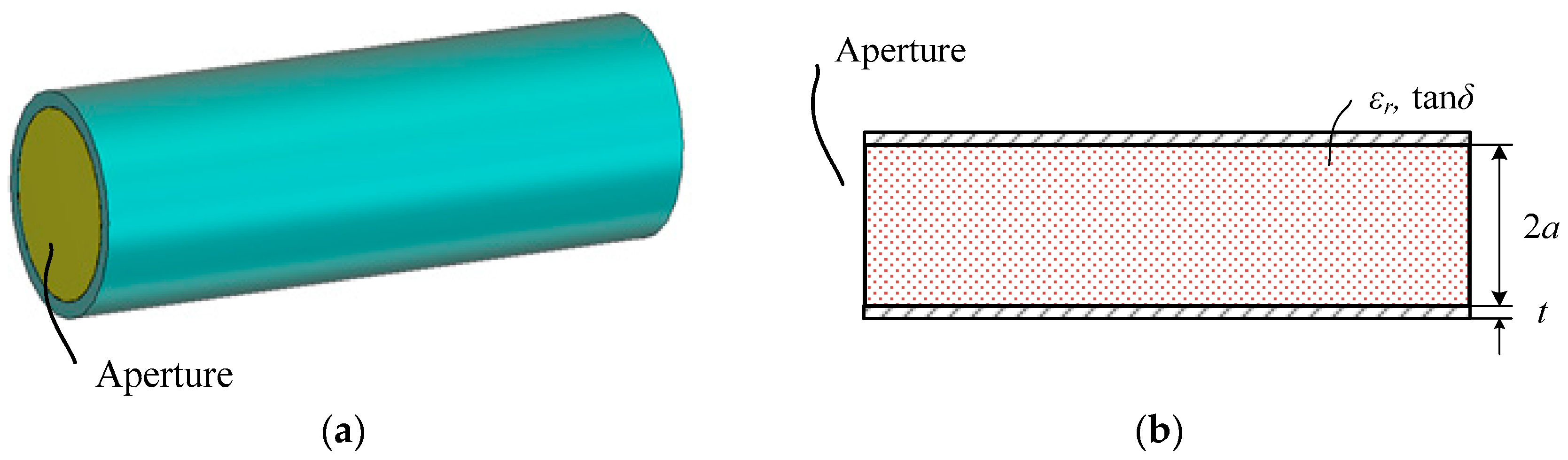
Figure 1 shows an unmatched circular waveguide aperture. The waveguide inner wall diameter is 2a and the wall thickness is t. The waveguide is filled with a low-loss material with dielectric constant εr and loss tangent tanδ. The dielectric filling lowers the operating frequency or reduces the waveguide diameter for a given operating frequency. For high size-reduction ratios, the dielectric constant of the filling material needs to be high, and this will greatly increase the reflection at the aperture.
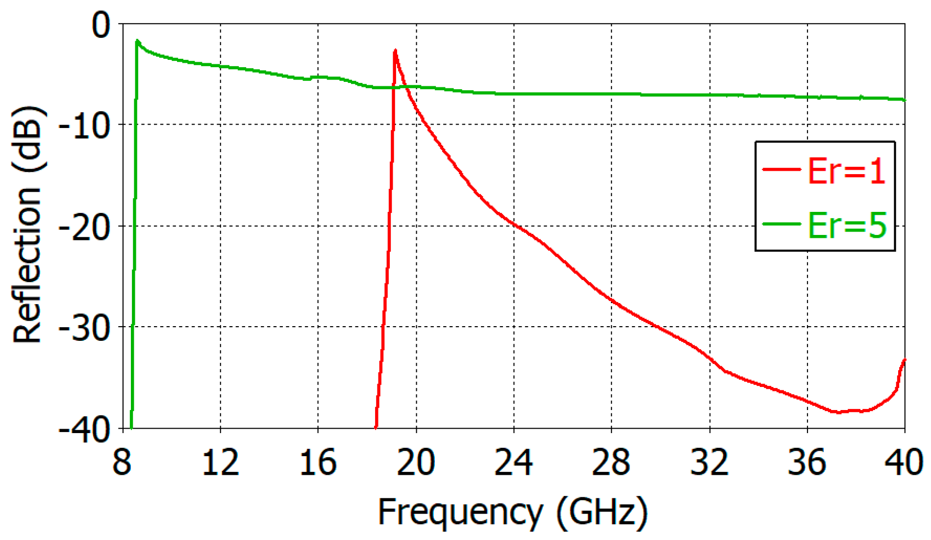
Figure 2 shows the reflection coefficient of the apertures of an unfilled circular waveguide and of a circular waveguide filled with a material of εr = 5.0. The waveguide diameter 2a is 9.20 mm and the wall thickness t is 0.80 mm. In Figure 2, one can observe a dramatic increase in the reflection coefficient when the waveguide is filled with a material of εr = 5.0. In an unfilled circular waveguide, the dominant TE11-mode cutoff frequency (fcTE11) is 19.10 GHz, and the reflection coefficient reaches −10 dB at 20.43 GHz (1.070fcTE11) and a minimum value of −38.4 dB at 37.36 GHz. With εr = 5.0, the dominant TE11-mode cutoff frequency (fcTE11) is 8.54 GHz and the reflection coefficient reaches −2.11 dB at 8.67 GHz (1.015fcTE11) and a plateau value of −6.9 dB at 22.48 GHz.
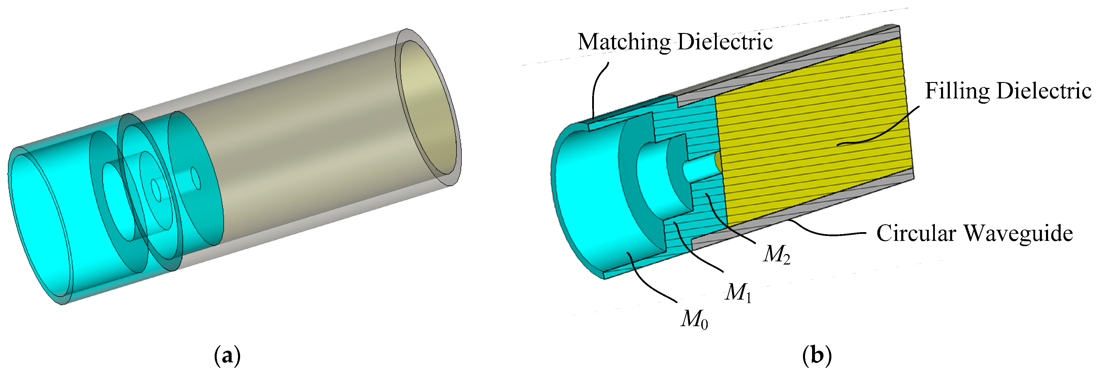
A simple and innovative method of the aperture matching proposed in this paper is depicted in Figure 3. A circular waveguide is filled with a dielectric material of dielectric constant εr and loss tangent tanδ in the same way as in Figure 1. The same dielectric material as the filling material is placed in the waveguide open end for aperture matching. Broadband impedance matching is obtained by forming the matching material in a shape of two or three stacked rings which can be created by carving out concentric cylindrical volumes in the center and filling the carved-out space with air. Carving out the edge portion of a dielectric cylinder, i.e., solid coaxial dielectric cylinders of varying diameter, does not give a broadband aperture matching. More than three stacked rings can yield a wider bandwidth, but two or three rings give a bandwidth large enough for practical applications.
The matching structure can be thought of as a three-section (M0, M1 and M2) impedance transformer that converts the circular waveguide TE11-mode wave impedance into the free-space planewave impedance. The function of the matching rings is to gradually transform the effective dielectric constant of the medium from εr of the dielectric-filled waveguide to 1 of the free space. The amount of the removed portion in the dielectric ring is increased as the wave propagates from the waveguide to the air, transforming the effective dielectric constant from εr to 1. In this way, the guided TE11-mode wave in the circular waveguide is smoothly transformed to the TEM-mode planewave in the air. A broadband impedance matching is possible by proper dimensioning of the two or three concentric rings.
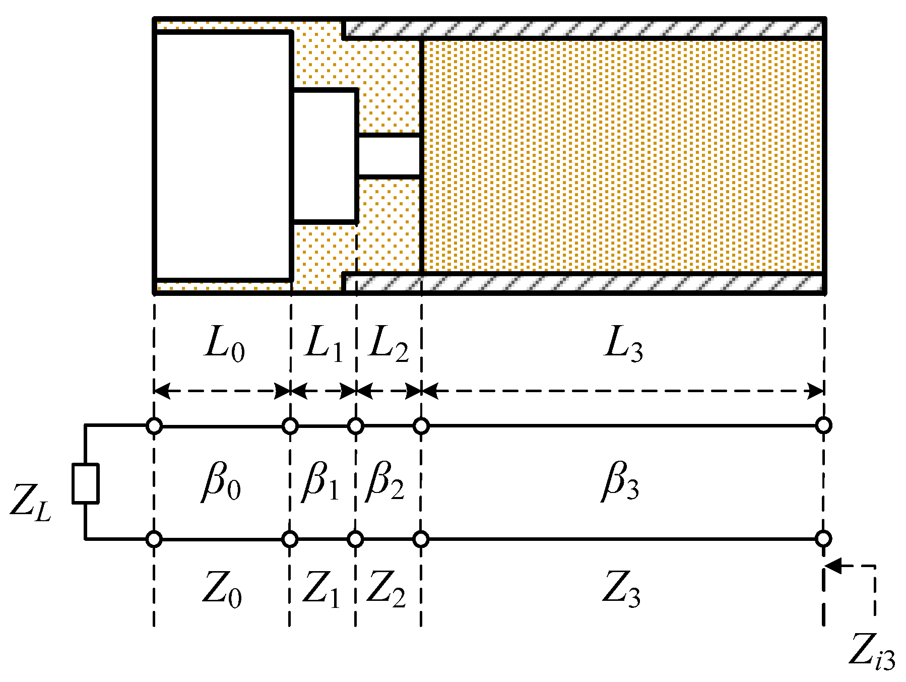
Figure 4 shows a simplified equivalent circuit model of the proposed aperture matching structure. The parameter ZL is the characteristic impedance of the free space in front of the first matching element M0. The parameters Z0, Z1, Z2 and β0, β1, β2 and L0, L1, L2 are the characteristic impedance, propagation constant and length in the equivalent transmission line representation of the matching sections M0, M1 and M2, respectively. The parameters Z3, β3 and L3 are the characteristic impedance, propagation constant and length of the dielectric-filled circular waveguide, respectively. The parameter Zi3 is the input impedance at the circular waveguide port.
From the equivalent circuit model, the input reflection coefficient Γ at the circular waveguide port is obtained using
Γ = (Zi3 − Z3)/(Zi3 + Z3)
The reflection coefficient Γ0 after the matching section M0 is given by
where ΓL is the reflection coefficient at the input of M0 given by
Γ0 = ΓLexp(−j2β0L0)
ΓL = (ZL − Z0)/(ZL + Z0)
The impedance Zi0 at the input of the second matching element M1 is obtained from Γ0 using
Zi0 = Z0 (1 + Γ0)/(1 − Γ0)
By repeatedly applying Equations (2)–(4), we calculate Zi1, Zi2, and Zi3, from which we obtain the input reflection coefficient Γ given by (1).
The equivalent circuit model of Figure 4 will give accurate results if true values of the model parameters are used and the dielectric junction effect is included. A rigorous evaluation of the model parameters and the junction effect is very complicated if not impossible. Firstly, for a non-TEM transmission line, the characteristic impedance can be defined using the VI-definition, or the PV-definition or the PI-definition [35]. One has to determine on a theoretical basis which definition to use. Secondly, a simple transmission line model is not good enough for the proposed matching structure due to the fringing field in the aperture. The field near the aperture does not conform to that of a uniform transmission line where the transverse distribution of the electric and magnetic fields is invariant along the direction of wave propagation. Thirdly, the discontinuity effect of the dielectric step junction is difficult to model due to the complicated field structure of the aperture. Therefore, it is better to use an equivalent circuit model for the elucidation of the operating principles and to employ the numerical simulation and optimization for the actual design of the proposed matching structure.
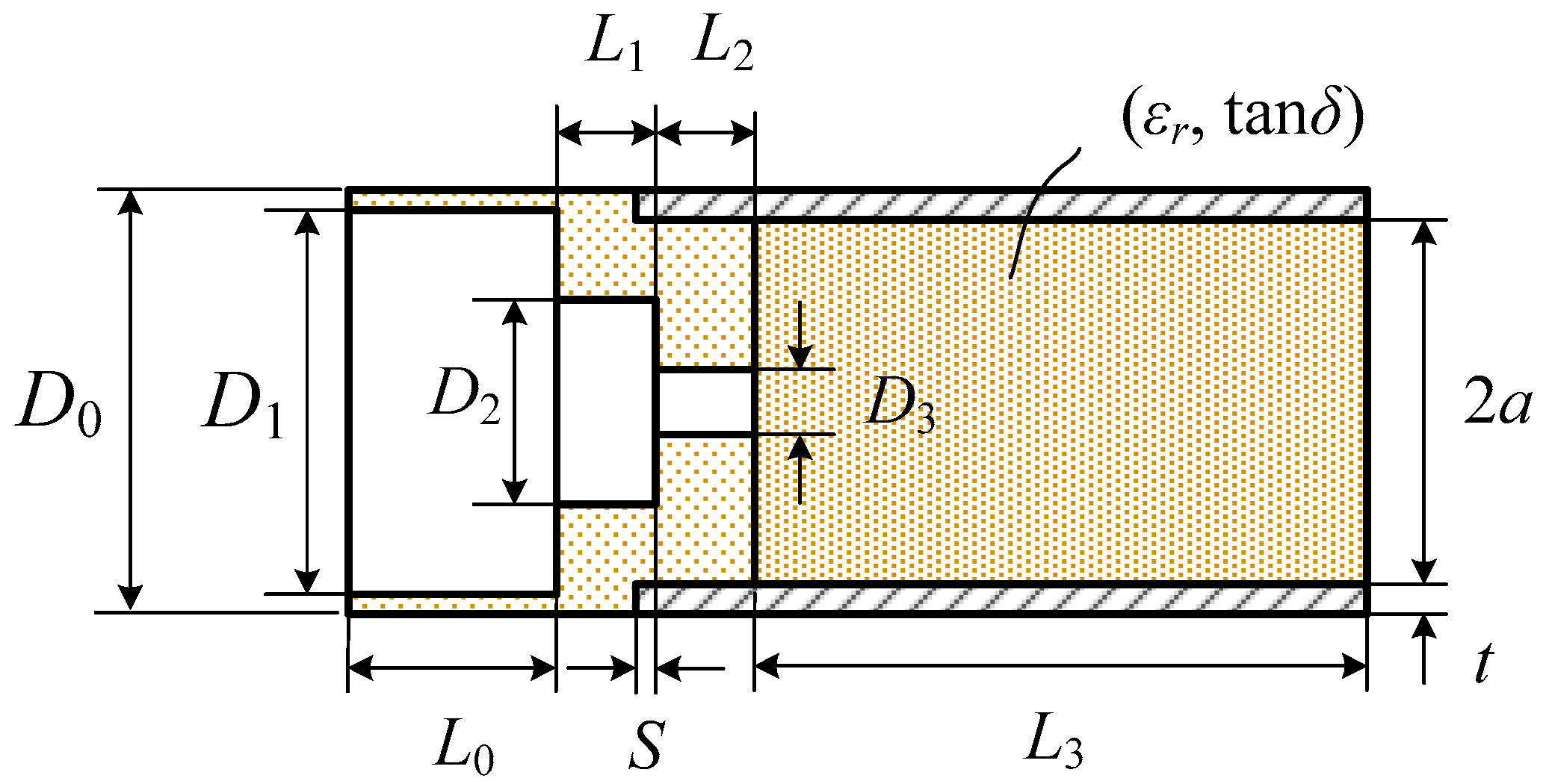
Figure 5 shows the dimensional parameters of the proposed matching structure. Fixed values of 9.20, 20.00 and 0.90 mm have been used for the inner wall diameter 2a, length L3 and wall thickness t of the circular waveguide. The parameter S is the position of the interface between the second (M1) and third (M2) matching sections relative to the end of the waveguide wall. It is positive if the M1-M2 interface is into the circular waveguide and negative otherwise. D0 is the diameter of the matching dielectric’s portion that is outside the waveguide. D0 is fixed at 2a + 2t. The remaining parameters are the hole diameters D1, D2, D3 and the lengths L0, L1 and L2 of the matching sections M0, M1 and M2, respectively.
The loss tangent (tanδ) of the filling and matching dielectric materials is fixed at 0.0008. A higher value of the loss tangent will not affect the aperture matching as far as it is small enough, for example, less than 0.008. It will, however, increase the attenuation of the waveguide. Power loss in a uniform transmission line is given by
where z is the propagation distance and β is the propagation constant of the waveguide TE11 mode. The power loss factor P/P0 of a one-wavelength long waveguide is 0.975 and 0.997 for tanδ of 0.008 and 0.0008, respectively. The impedance matching is controlled by the effective dielectric constant of the matching rings, which is in turn determined by the carved-out volume. Since the length of the impedance matching structure is not large—less than 1.35 times the waveguide diameter, as shown below in the design examples—the impedance matching performance is virtually the same for a loss tangent of 0.008 and 0.0008. This can easily be checked by simulation.
P = P0 exp(−βztanδ)
Starting from initial values D1 = 0.75(2a), D2 = 0.5(2a), D3 = 0.25(2a), L0 = L1 = L2 = 0.5(2a), S = 0, these parameters are optimized for εr = 1.8, 2.5, 5.0, 7.5 and 10.0 using CST Studio SuiteTM V2023 for low reflection over as broad a frequency range as possible with the start frequency (reflection < −10 dB) as close as possible to the TE11-mode cutoff frequency of the dielectric-filled circular waveguide. For the two-section matching structure, the first matching section length L0 is set to zero.
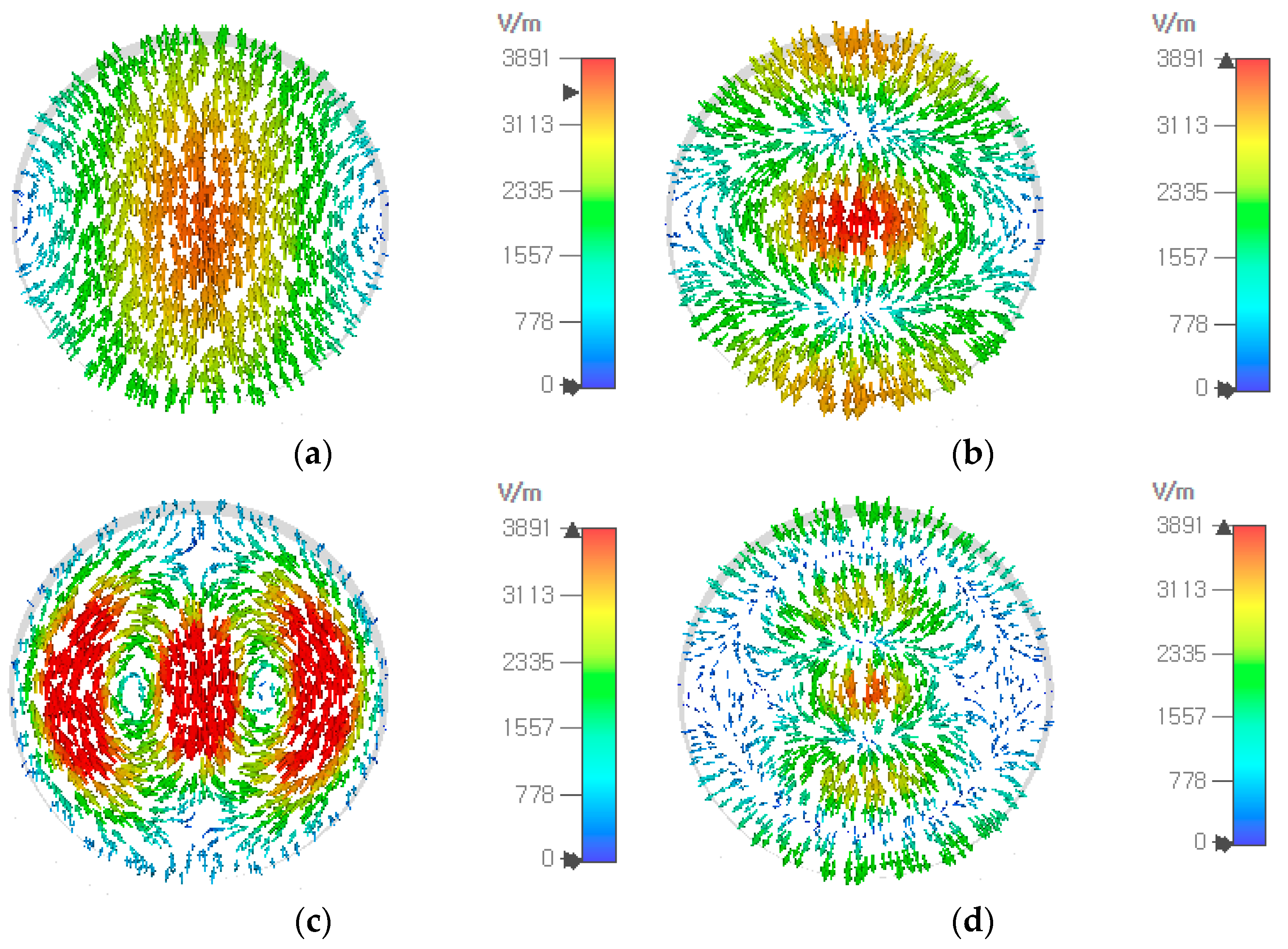
In designing an aperture-matched circular waveguide radiator, it is necessary to analyze the higher-order modes generated along with the fundamental TE11 mode. In a circular waveguide, the first 15 higher-order modes in the order of increasing cutoff frequencies are TE11, TM01, TE21, TE01/TM11, TE31, TM21, TE41, TE12, TM02, TM31, TE51, TE22 and TE02/TM12. The modes with the electric field being symmetric in the E and H planes, nonzero at the waveguide center and irrotational in the waveguide transverse plane, are easily excited when the fundamental TE11 mode is launched by a probe, a slot or other methods. They include TM11, TE12 and TM12 modes whose electric fields at 73 GHz have been obtained using CST Studio SuiteTM V2023 and are shown in Figure 6. The cutoff frequency of these modes in a 9.20-mm diameter waveguide is given in Table 3, including the εr = 1 case.
By employing symmetric structures, it is possible to operate a circular-waveguide-based device from the TE11-mode cutoff to the TM11-mode cutoff. The cutoff frequency fc,TM11 of the TM11 mode is 2.08 times the fundamental TE11-mode cutoff frequency fc,TE11. Allowing for a guard band of 5% at fc,TE11 and fc,TM11, the frequency range will be from 1.05 fc,TE11 to 0.95 fc,TM11 (=1.98 fc,TE11) or a ratio bandwidth of 1.98/1.05 = 1.89. Since the level of the TM11-mode generation is dependent on a specific geometry of structures to be used in the waveguide, it is possible to operate a circular waveguide device above the TM11 mode cutoff. For example, Bang and Ahn have proposed a coaxial-to-circular waveguide transition operating with a ratio bandwidth of 2.18 [36].
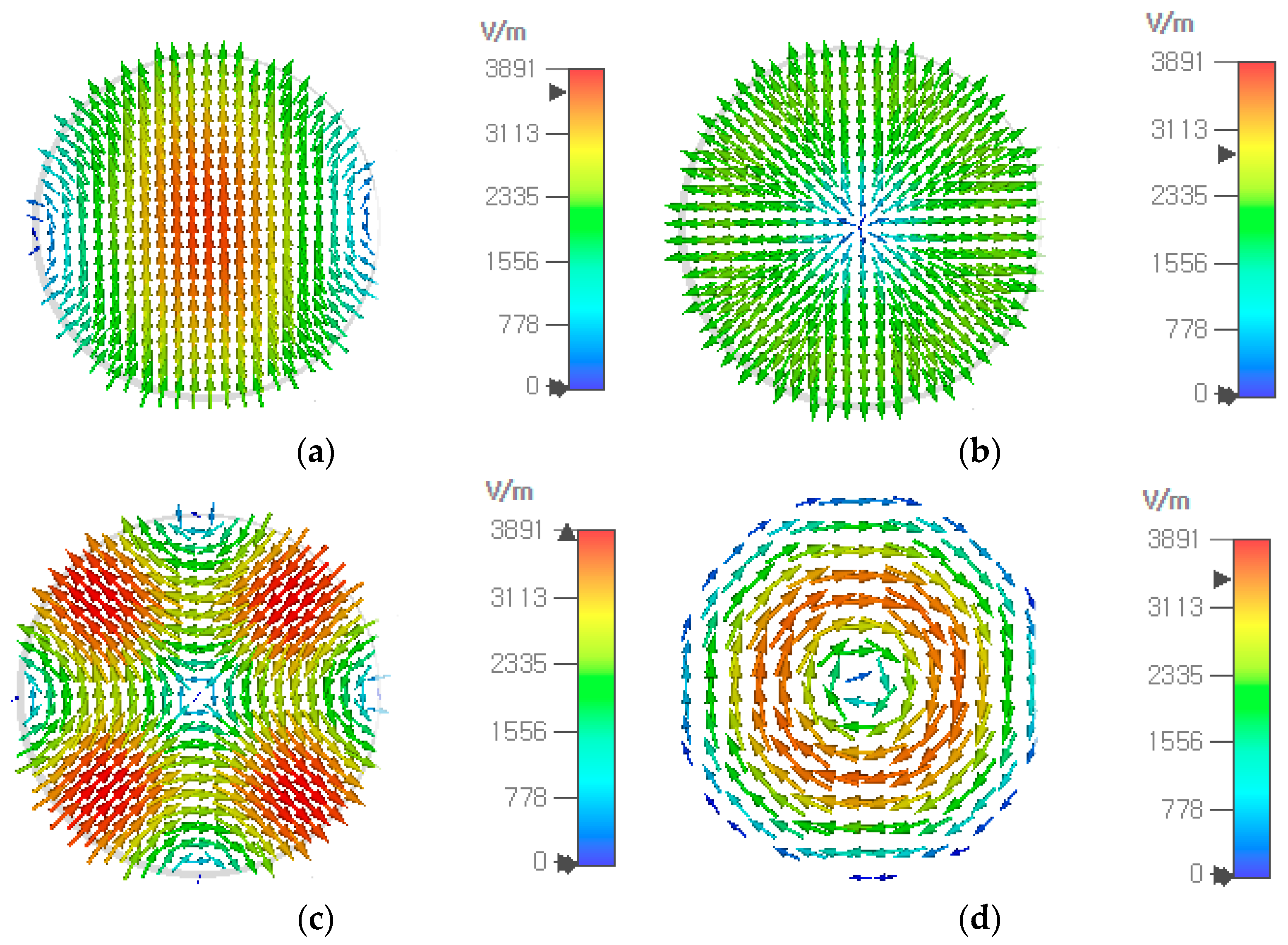
The modes with the electric field being antisymmetric in the E and H planes, or zero at the waveguide center, or rotational in the waveguide transverse plane, are not easily excited when the fundamental TE11 mode is launched, the first three of which are TM01, TE21 and TE01, whose cutoff frequencies are 1.31, 1.66 and 2.08 times the fundamental TE11-mode cutoff frequency, respectively. With εr = 1 and 2a = 9.20 mm, they are 24.94, 31.68 and 39.74 GHz. Figure 7 shows the electric field of these three modes along with the TE11 mode at 44 GHz.
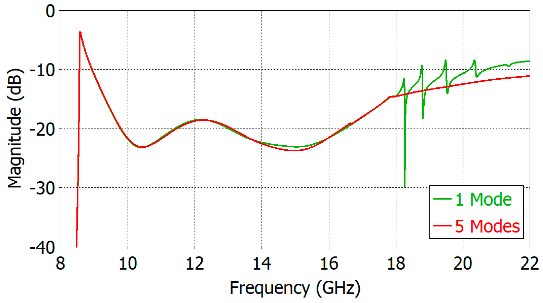
In simulating a circular waveguide over a broad frequency range, the inclusion of the higher-order modes whose cutoff is in the frequency range of analysis has an effect on the reflection coefficient of the fundamental TE11 mode. Figure 8 shows the effect on the reflection coefficient of the higher-order modes in the frequency-domain analysis of a two-section matching structure with a filling material of εr = 5.0. When only the TE11 fundamental mode is terminated properly (i.e., no reflection) but all higher-order modes are not included (i.e., total reflection), many resonance spikes appear due to multiple reflections of the higher-order modes between the aperture and the port plane. If we include five modes (TE11 mode + the first four higher-order modes TM01, TE21 and TE01/TM11), the spikes in the reflection coefficient will disappear. In the actual implementation of the proposed aperture matching structure, the termination condition of the higher-order modes depends on a device connected to the circular waveguide port.
In Figure 8, the resonance spikes occur at four frequencies; 18.27, 18.77, 19.48 and 20.36 GHz. The cutoff frequencies of the TM01, TE21, TE01/TM11, TE31 and TM21 modes in this waveguide are 11.16, 14.17, 17.77/17.77, 19.49 and 23.82 GHz, respectively. It is important to note that the resonance spikes occur at frequencies larger than the TM11 cutoff. In the design of the proposed matching structure, the frequency upper limit is set to the onset of the first resonance spike. The proposed matching structure can be used beyond the first resonance spike frequency if the generation of the TM11 mode is properly suppressed.
The optimization of the matching structure dimensions is performed in the following steps. The target frequency range for impedance matching optimization is set from the start frequency f1 = 1.01fc,TE11 to the end frequency f2 = 2fc,TE11, where fc,TE11 is the dominant TE11-mode cutoff frequency in the dielectric-filled circular waveguide given by
fc,TE11 = 299.792/(1.70629(2a)√εr)
In the first step of the design, a parametric analysis is carried out for the reflection coefficient versus dimensional parameters to find out the range of parameter values to be set in the optimization. The dimensions of the designed matching structure have been obtained using the ‘Trust Region Framework’ optimization algorithm provided by CST Studio SuiteTM V2023. The optimized design is typically obtained after 200 to 300 hundred iterations, which takes several hours on a desk-top computer.
Next, a first round of optimization is carried out for a target reflection coefficient of −10 dB, and optimum dimensions are obtained. With the dimensions obtained in the first round of optimization and the target reflection coefficient set at −15 dB, a second-round optimization is completed. Using the dimensions obtained in the second optimization round and with the reflection coefficient set at −20 dB, a third round of optimization is carried out. After the third round of optimization, good results are usually obtained.
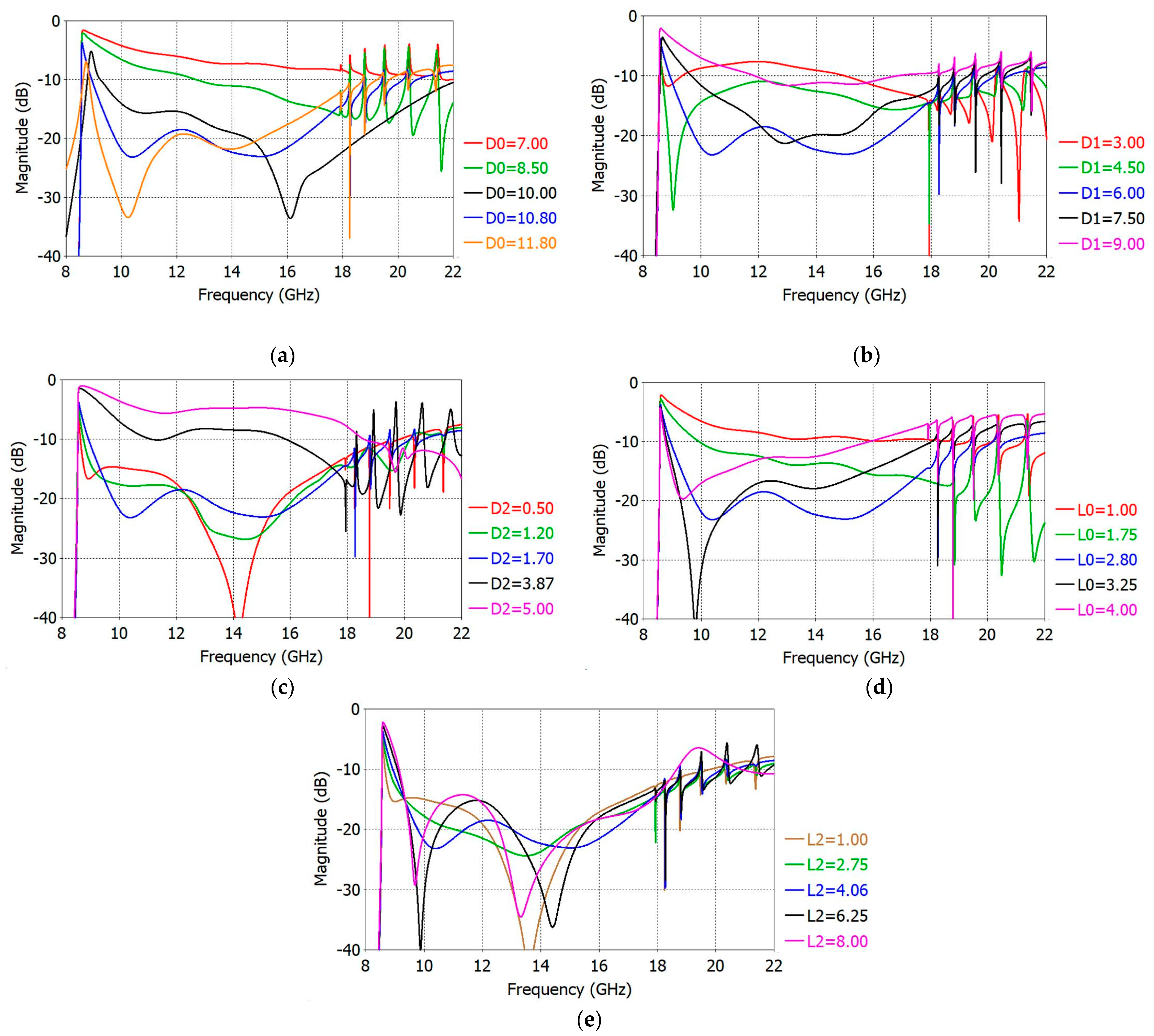
Following the aforementioned procedures, we were successful in obtaining good aperture matching for εr from 1.8 to 10. Figure 9 shows the reflection coefficient versus dimensional parameters of a two-section aperture matching design for εr = 5.0. The curve in blue is for the reflection coefficient after optimization. In Figure 9, the spikes in the reflection coefficient at f > 18 GHz are caused by the exclusion of the higher-order modes in the waveguide port. As stated in the above, the resonance spikes are not generated if higher-order modes are included in the simulation. One design may require the lowest operating frequency with reflection < −10 dB and another design the lowest reflection at a specified frequency range. In Figure 9, one can see that this design flexibility is possible with a proper choice of dimensional parameters.
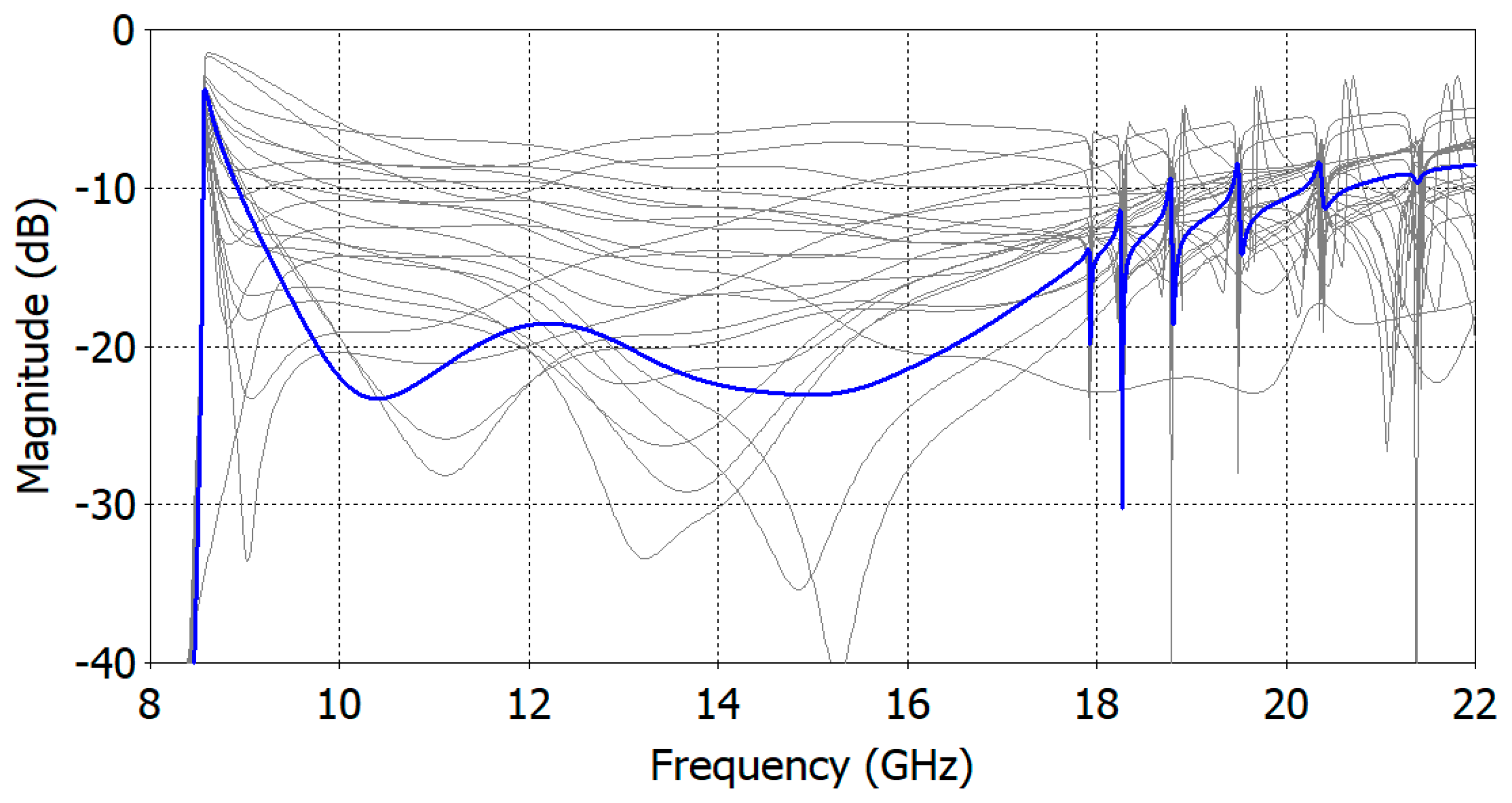
Figure 10 shows the change in the reflection coefficient during an optimization by CST Studio SuiteTM V2023. Starting from a high reflection coefficient, an optimization process finds the dimensions of the matching structure for a target reflection coefficient over a specified frequency range.
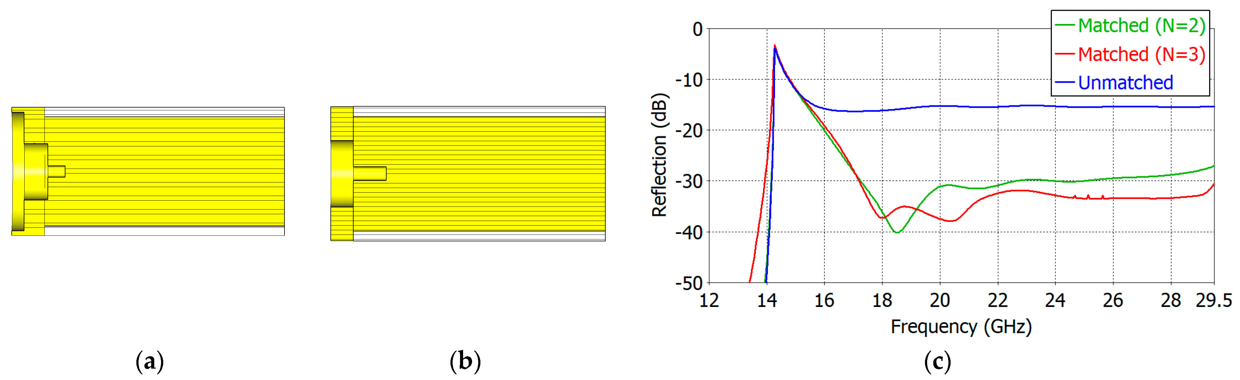
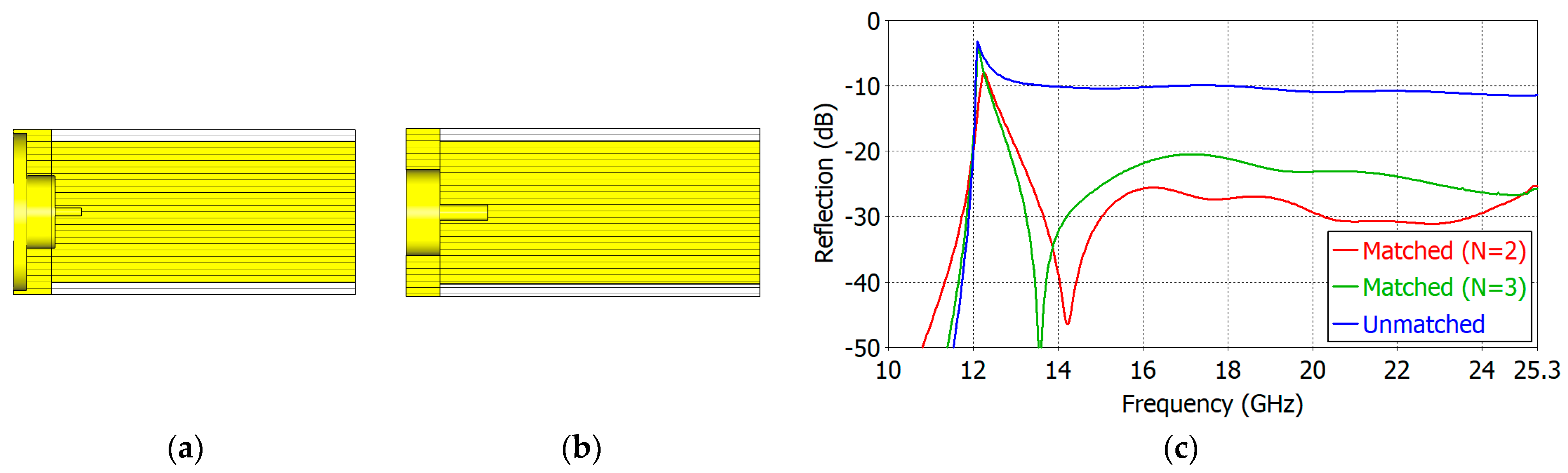
We have carried out aperture matching designs for εr = 1.8, 2.5, 5.0, 7.5 and 10.0. We have made the lower limit of the operating frequency as close to the TE11-mode cutoff frequency as possible while maintaining a low reflection coefficient over a broad frequency range. Table 4 and Table 5 show the dimensions of the designed two- and three-section matching structures, respectively. The cross-section of the respective matching structure is also shown in Figure 11, Figure 12, Figure 13, Figure 14 and Figure 15.
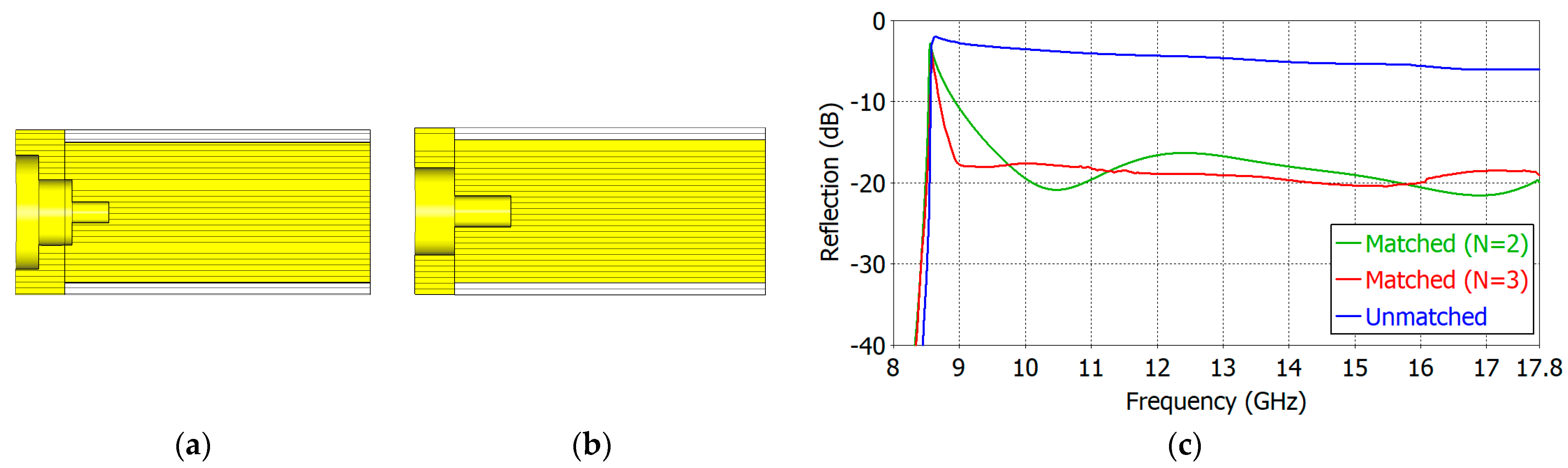
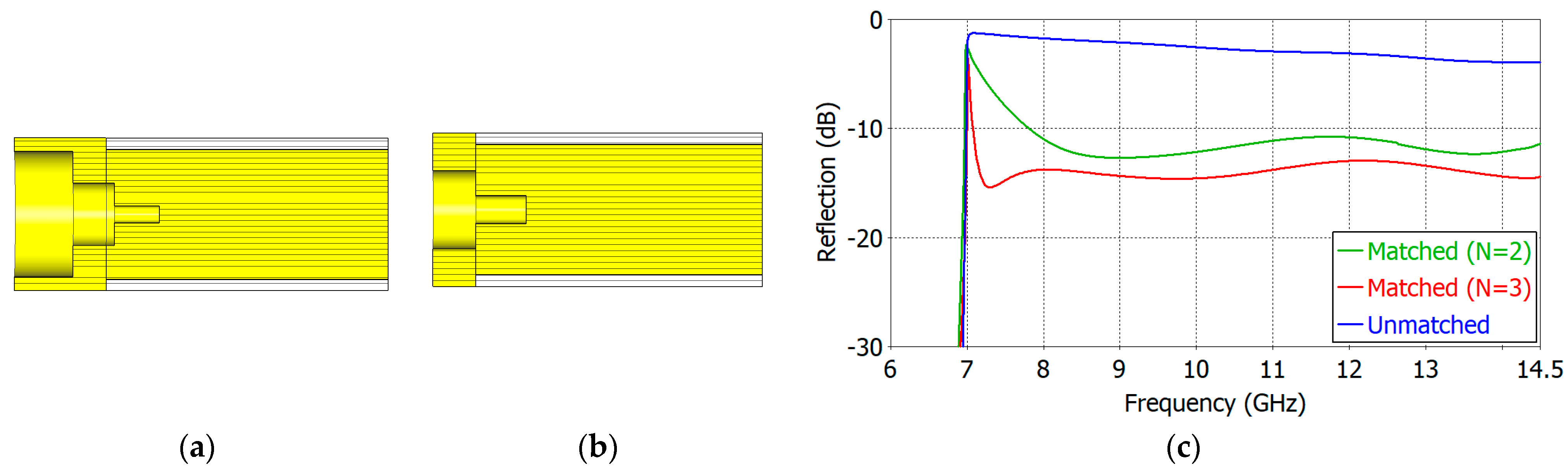
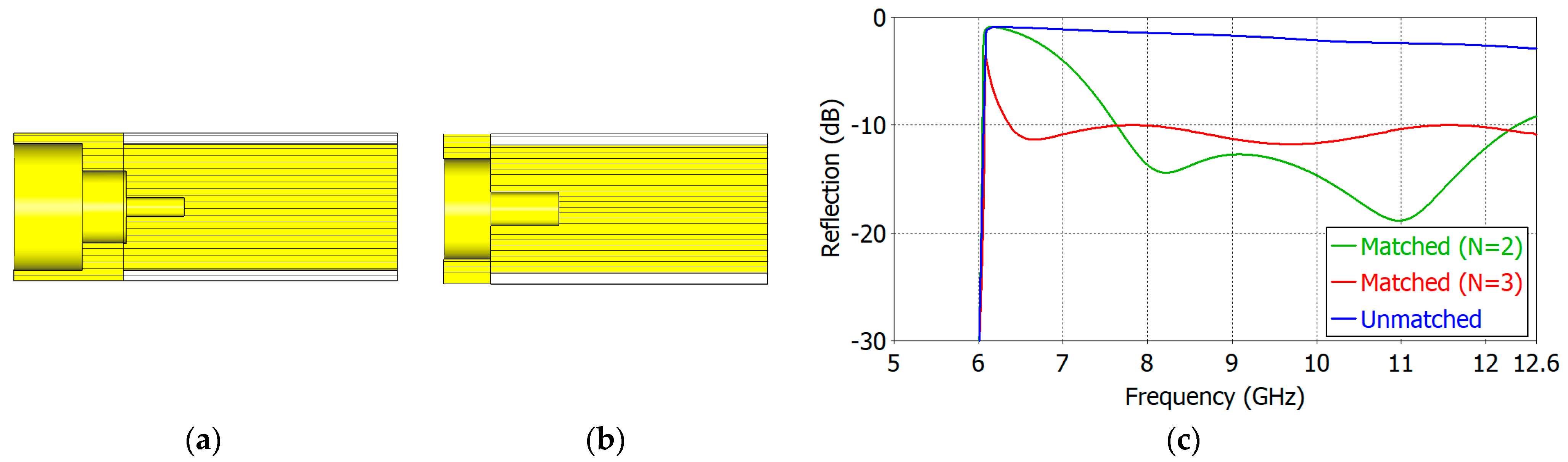
Figure 11, Figure 12, Figure 13, Figure 14 and Figure 15 show the cross-section and the reflection coefficient of the aperture-matching structure with εr = 1.8, 2.5, 5.0, 7.5 and 10.0, respectively. The frequency range in the figures is from a little below the TE11-mode cutoff to the onset of the spikes in the reflection coefficient. In all the cases, the reflection coefficient is dramatically reduced with the three-section (N = 3) matching as well as with the two-section (N = 2) matching. The three-section matching makes a starting frequency closer to the TE11-mode cutoff than the two-section matching and thus offers a wider bandwidth. The aperture matching can also be designed for a smaller reflection coefficient over a narrower frequency range.
Table 6 and Table 7 summarize the performance of the proposed aperture matching design with two- and three-section structures for εr = 1.8, 2.5, 5.0, 7.5 and 10.0. The unmatched circular waveguide aperture has a reflection coefficient of less than −10 dB for εr = 1.8 and 2.5. With dielectric constants of 5.0, 7.5 and 10.0, the unmatched reflection coefficient ranges from −6.0 to −0.9 dB, while with the proposed aperture matching the reflection coefficient is reduced to the −20 to −10 dB level.
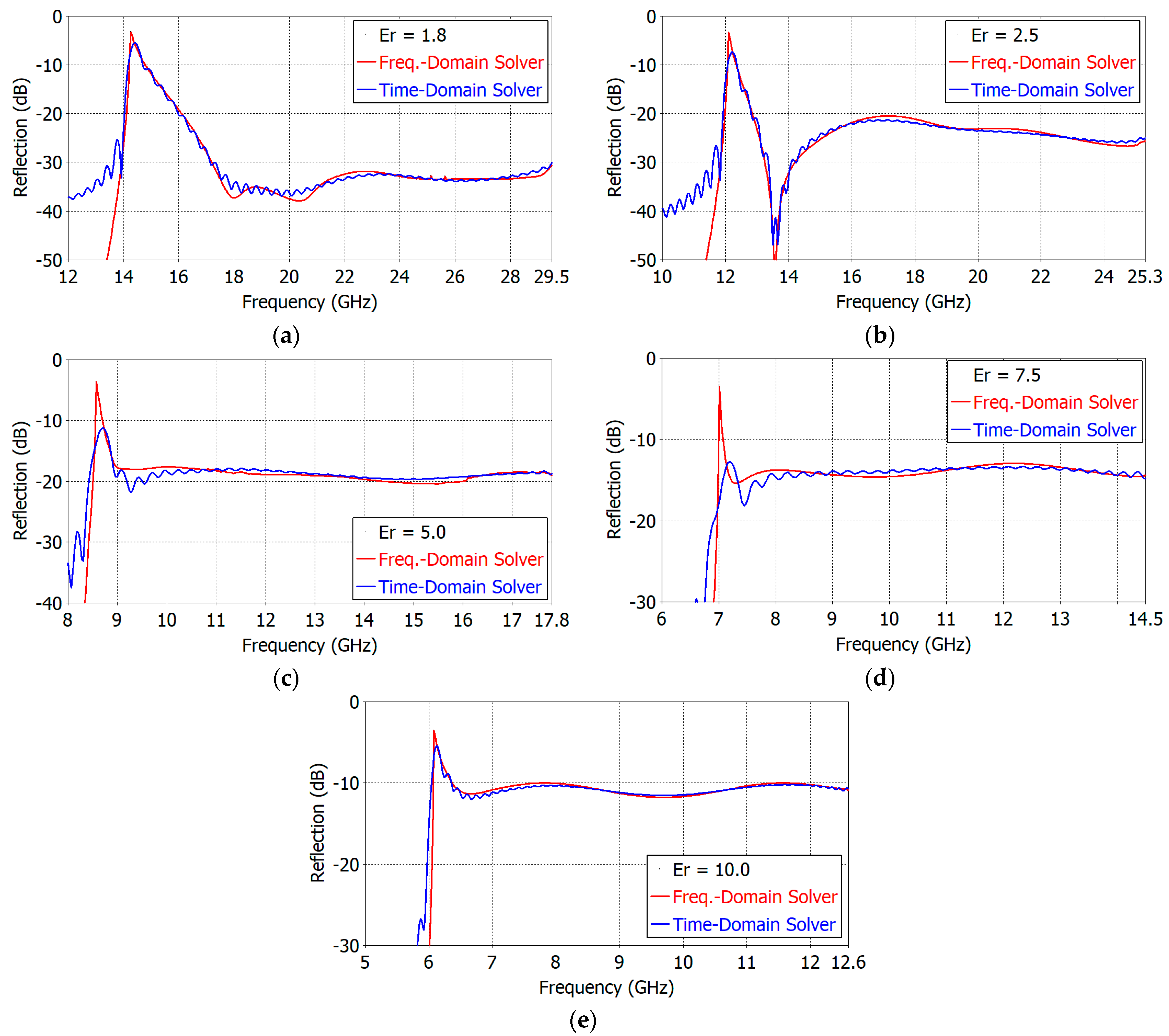
In order to ascertain the simulation accuracy, we compared, in Figure 16, the reflection coefficients of the three-section matching structure computed using the frequency- and time-domain solvers for εr from 1.8 to 10.0. The agreement between two simulation methods is excellent.
In Figure 11, Figure 12, Figure 13, Figure 14 and Figure 15, one can observe that the length of the matching structure is not large compared with the waveguide diameter. Table 8 and Table 9 summarize the matching structure lengths outside and inside the waveguide for the two- and three-section cases, respectively. The length of the outside portion ranges from 0.20 to 0.37 times the waveguide diameter (2a) in the two-section matching (N = 2) and from 0.30 to 0.87 times 2a in the three-section matching (N = 3), while the length of the inside portion ranges from 0.28 to 0.54 times 2a for N = 2 and from 0.19 to 0.48 times 2a for N = 3. The total length of the matching structure ranges from 0.48 to 0.91 times 2a for N = 2 and from 0.49 to 1.35 times 2a for N = 3. The compactness is one of the merits of the proposed matching structure.
Table 10 summarizes the impedance matching performance of the proposed three-section matching structures. As the dielectric constant εr varies from 1.8 to 10.0, the reflection coefficient (|S11|) plateau increases from −31.7 dB to −10.0 dB. The ratio bandwidth for the reflection coefficient of less than the plateau reflection coefficient ranges from 1.68 to 2.01. A special merit of the proposed matching technique is that the start frequency (fS) for |S11| < −10 dB is very close to the TE11-mode cutoff, ranging from 1.015–1.051.
The reflection coefficient of the unmatched circular waveguide aperture at fS ranges from −10.7 dB to −0.93 dB for εr from 1.8 to 10. If the aperture matching is carried out inside the waveguide to match an aperture with a reflection coefficient in the order of −3 dB to −1 dB, it will inevitably result in a very narrow bandwidth. In the proposed technique, however, the aperture matching starts outside the waveguide and ends inside the waveguide. The outside portion significantly reduces the aperture reflection, and a further reduction in reflection is carried out by the inside portion.
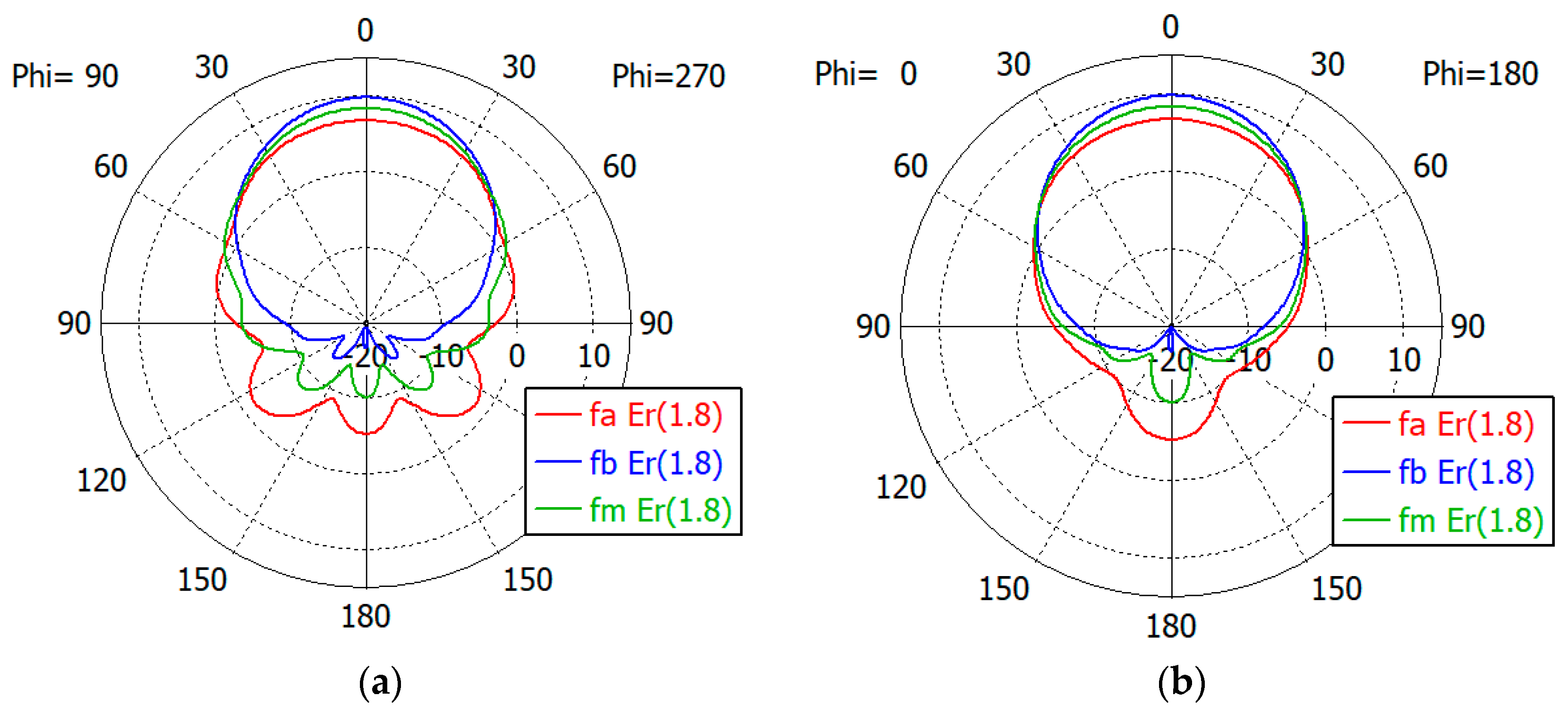
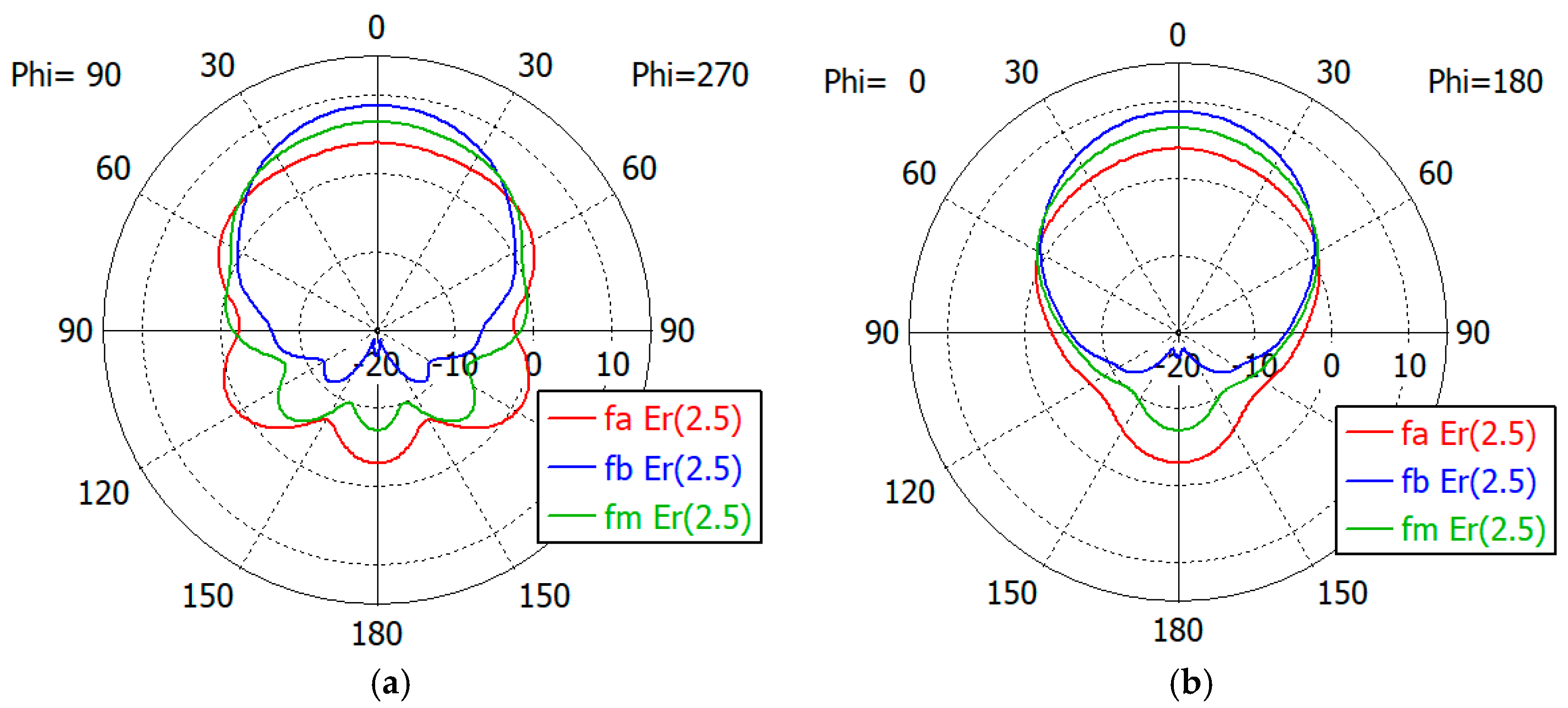
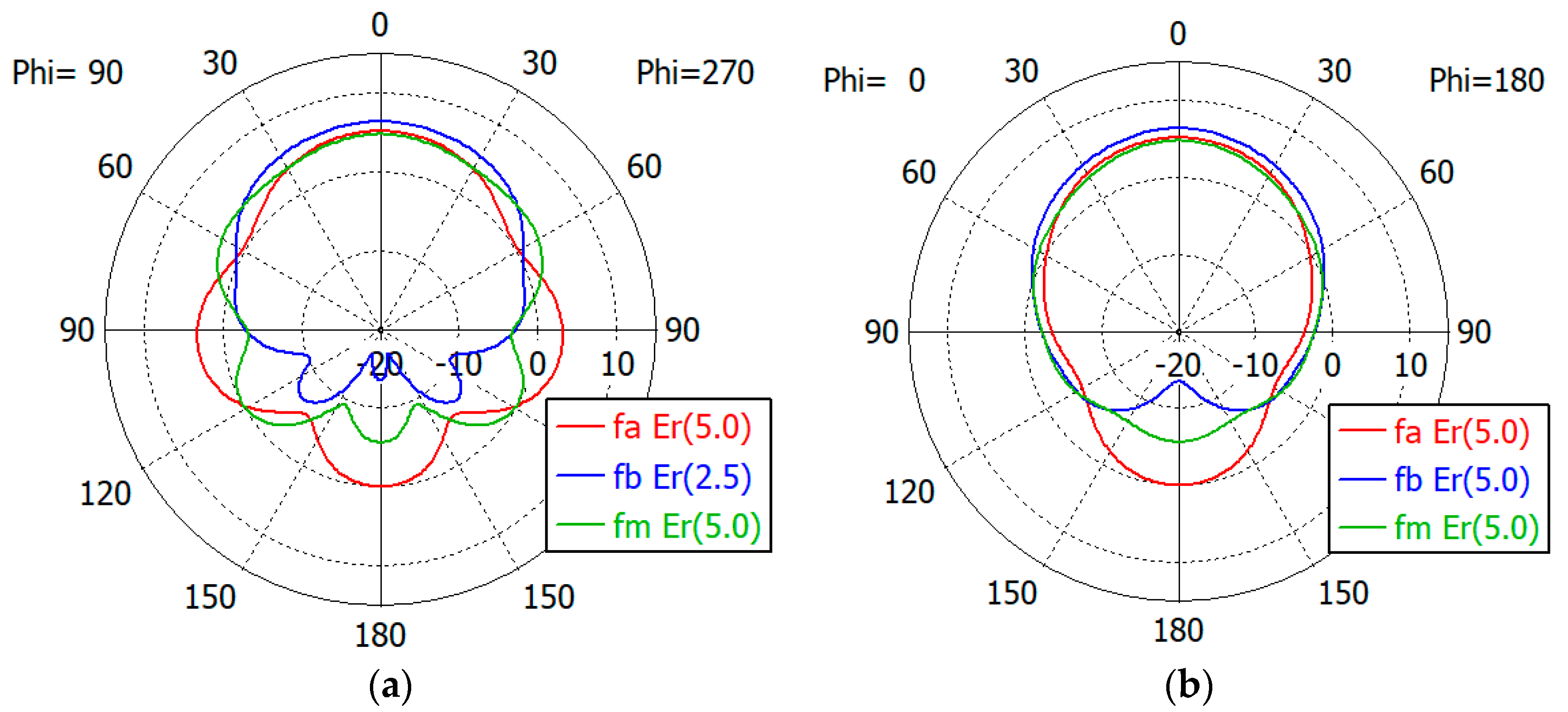
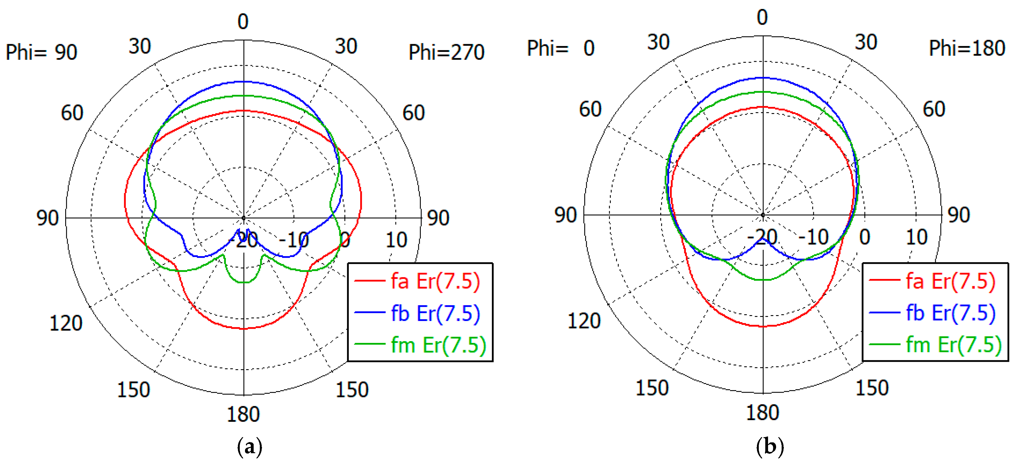
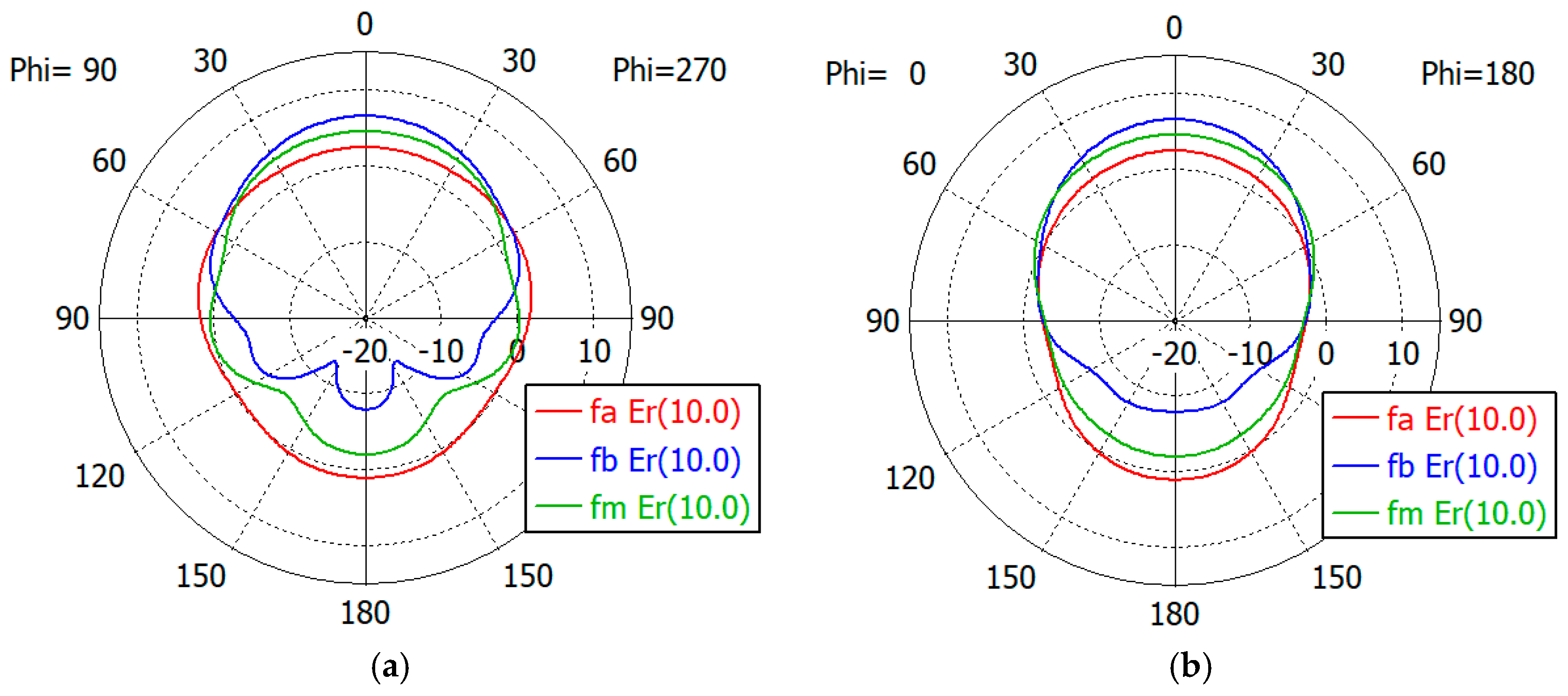
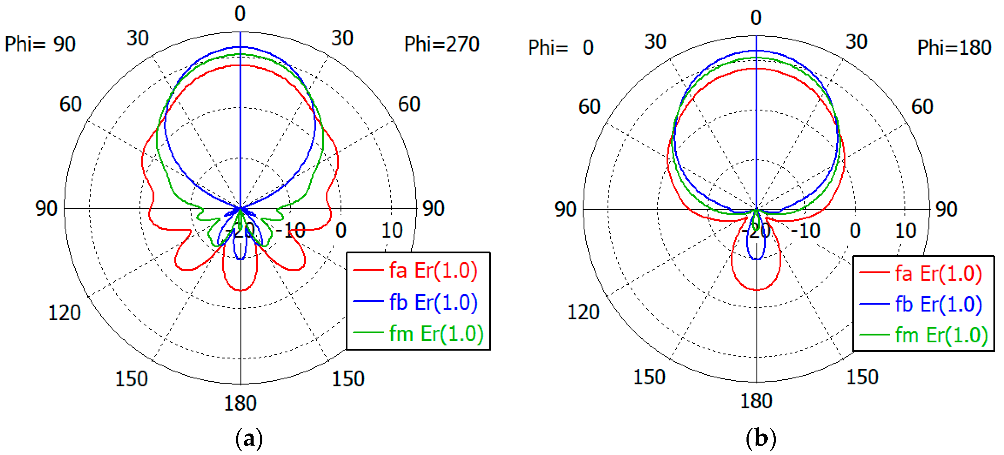
Figure 17, Figure 18, Figure 19, Figure 20 and Figure 21 show the E- and H-plane gain patterns of the designed matching structures with three-section matching, where fa is the start frequency for the reflection coefficient plateau and fm and fb are the middle and end frequencies of the plateau. For comparison, we present Figure 22 for an unfilled circular waveguide open end of the same diameter, where fa is the start frequency for the reflection coefficient < −10 dB, fm is the frequency for 2a = λ and fb is 40 GHz, an arbitrary upper frequency.
The aperture-matched dielectric-filled waveguide radiator shows gain patterns similar to those of an unfilled case. The maximum gain decreases as the dielectric constant increases, since the aperture dimension decreases compared to the wavelength in the air. For a given dielectric constant, the aperture’s gain increases as the frequency increases, except in the cases with εr = 5.0, where the gain at fa is slightly larger than the gain at fm. At the start frequency, the gain in the backward direction (θ = 180°) is relatively large; −3.3 dBi with εr = 1.0, and −5.0 dBi to 1.7 dBi with εr from 1.8 to 10.0.
Table 11 summarizes the waveguide diameter 2a normalized by the wavelength in vacuum at the start frequency fa for the plateau reflection coefficient. Table 11 also shows the gain of the waveguide aperture at the start (fa), middle (fm) and end (fb) frequencies for the plateau reflection coefficient. The frequencies fa and fb are listed in Table 10. The aperture’s gain ranges from 6.7 dBi to 1.0 dBi at fa, from 10.1 dBi to 4.0 dBi at fm and from 12.1 dBi to 6.5 dBi at fb for εr from 1.8 to 10. Table 11 also lists the gain of an air-filled waveguide aperture of the same diameter for comparison. The gain in this case is greater than that of the dielectric-filled aperture, since the operating frequency is higher. In Table 11, we note that with εr = 10, the waveguide diameter is only 0.19 times the wavelength at fa, where the matched reflection coefficient is −10 dB, while the unmatched reflection coefficient is only −0.19 dB. We think that this is a remarkable result, which has not been achieved until now.
Table 12 compares the bandwidth performance of the proposed matching structures with previous works. First, we should mention that we could not compare the bandwidth under an equal condition since sufficient data have not been provided in previous works. In the proposed matching structures, the plateau reflection coefficient ranges from −31.7 dB to −13.1 dB for εr from 1.8 to 7.5. If we use the condition |S11| < −10 dB in these cases, the bandwidth will be increased a little further. In [4], the frequency range for |S11| < −10 dB is not fully drawn. Therefore, bandwidth for |S11| < −20 dB is used in Table 12.
Even with the limited data provided in previous works, we can say that the level of bandwidth achievable with the proposed matching structure has not been heard of. In addition to the broadband aperture matching, the proposed method achieves |S11| < −10 dB very close to the cutoff frequency, maximizing the size reduction ratio. The proposed aperture matching structure is so simple that it can easily be machined or formed. For mechanical strength, the void air space in the matching rings can be filled with a material of low dielectric constant (1.03 ≤ εr ≤ 1.30) with a subsequent adjustment of dimensional parameters.
3. Conclusions
A simple and innovative method has been presented for the broadband matching of a dielectric-filled circular waveguide aperture. By loading the aperture with two- or three-section dielectric rings, broadband impedance matching has been possible for the dielectric constant of the filling material ranging from 1.8 to 10.0. The dimensions of the matching structure have been obtained by computer-based optimization. The proposed matching structure is compact as well as geometrically simple so that it can easily machined or formed. With three-section matching rings, we have achieved a ratio bandwidth from 1.68 to 2.01 for a reflection coefficient ranging from –31.7 dB to –10.0 dB with a circular waveguide filled with a material with dielectric constants of 1.8, 2.5, 5.0, 7.5 and 10.0. With a dielectric constant greater than 5.0, the unmatched reflection coefficient ranging from −6.0 dB to −0.9 dB has been reduced to −20.4 dB to −10 dB. Start frequency for the reflection coefficient <–10 dB is very close to the TE11-mode cutoff, ranging from 1.015 to 1.051 times the TE11-mode cutoff frequency, which maximizes the size reduction ratio of the waveguide aperture. Existing methods of aperture matching of the dielectric-filled waveguide aperture do not provide a ratio bandwidth greater than 1.15. We expect that the proposed method would significantly contribute to the related art.
Author Contributions
Conceptualization, S.X.; methodology, S.X., J.H. and B.-K.A.; validation, S.X., B.-C.A. and C.-S.L.; formal analysis, B.-K.A. and B.-C.A.; invest, S.X., J.H. and C.-S.L.; writing—original draft, S.X.; writing—review and editing, B.-K.A. and B.-C.A.; supervision, B.-C.A. All authors have read and agreed to the published version of the manuscript.
Funding
This research was supported by Chungbuk National University Korea National University Development Project (2021) funded by the National Research Foundation of South Korea.
Institutional Review Board Statement
Not applicable.
Informed Consent Statement
Not applicable.
Data Availability Statement
The data presented in this study are available in this article.
Conflicts of Interest
The authors declare no conflict of interest.
References
- Amitay, N.; Galindo, V. The analysis of circular waveguide phased arrays. Bell Sys. Tech. J. 1968, 47, 1903–1932. [Google Scholar] [CrossRef]
- Li, Z.; Li, X.; Wan, C. Design of a Ka-band slant polarized circular waveguide phased array antenna. In Proceedings of the 9th Asia-Pacific Conference on Antennas and Propagation (APCAP), Xiamen, China, 4–7 August 2020. [Google Scholar]
- Gu, C.; Cheng, F.; Zhang, Z. Design of a compact D-band all-metal antenna fed by a circular waveguide. In Proceedings of the IEEE MTT-S International Microwave Workshop Series on Advanced Materials and Processes for RF and THz Applications (IMWS-AMP), Chongqing, China, 15–17 November 2021. [Google Scholar]
- Qudrat-E-Maula, M.; Shafai, L.; Pour, Z.A. Dielectric loaded circular waveguide feeds. In Proceedings of the 16th International Symposium on Antenna Technology and Applied Electromagnetics (ANTEM), Victoria, BC, Canada, 13–16 July 2014. [Google Scholar]
- Kehn, M.N.M.; Kildal, P.S.; Skobelev, S.P. Miniaturized dielectric-loaded rectangular waveguides for use in multi-frequency arrays. In Proceedings of the IEEE Antennas and Propagation Society International Symposium, Monterey, CA, USA, 20–25 June 2004. [Google Scholar]
- Liang, X.; Zhang, Z.; Zeng, J.; Guan, F.; Liu, X.; Zi, J. Scan blindness free design of wideband wide-scanning open-ended waveguide phased array. IEEE Access 2021, 9, 68127–68138. [Google Scholar] [CrossRef]
- Sporer, M.; Weigel, R.; Koelpin, A. Open-ended dielectric-filled waveguide antenna for underwater usage. In Proceedings of the 44th European Microwave Conference, Rome, Italy, 6–9 October 2014. [Google Scholar]
- Xu, D.; Li, Z.; Chen, X.; Wang, Z.; Wu, J. A dielectric-filled waveguide antenna element for 3D imaging radar in high temperature and excessive dust conditions. Sensors 2016, 16, 1339. [Google Scholar] [CrossRef] [PubMed]
- Chaudhury, D.N. An Investigation on the Possibility for Bandwidth Improvement of Dielectric Antennas via Modification of Their Geometry. Master’s Thesis, KTH Royal Institute of Technology, Stokholm, Sweden, 2020. [Google Scholar]
- C-Lec Plastics Inc. Available online: https://rexolite.com/rexolite/ (accessed on 7 October 2023).
- Riddle, B.; Baker-Jarvis, J.; Krupka, J. Complex permittivity measurements of common plastics over variable temperatures. IEEE Trans. Microw. Theory Tech. 2003, 51, 727–733. [Google Scholar] [CrossRef]
- Laird Technologies Inc. Eccostock® LoK. Available online: https://www.laird.com/products/microwave-absorbers/low-loss-dielectrics/eccostock-lok (accessed on 7 October 2023).
- Laird Technologies Inc. Eccostock® HIK500F. Available online: https://www.laird.com/sites/default/files/2021-01/RFP-DS-HIK500F.pdf (accessed on 7 October 2023).
- Laird Technologies Inc. Eccostock®.0005. Available online: https://www.laird.com/sites/default/files/2021-01/RFP-DS-0005%20112515.pdf (accessed on 1 November 2023).
- Cuming Microwave Corp. C-STOCK®.0005. Available online: https://www.cumingmicrowave.com/pdf/210-Dielectrics/210-3%20C-STOCK%20.0005.pdf (accessed on 1 November 2023).
- Laird Technologies Inc. Eccostock® HIK. Available online: https://www.laird.com/sites/default/files/2021-01/DS%20ECCOSTOCK%20HiK.pdf (accessed on 1 November 2023).
- Cuming Microwave Corp. C-STOCK® AK. Available online: https://www.cumingmicrowave.com/pdf/210-Dielectrics/210-1%20C-STOCK%20AK%20&%20AK-500.pdf (accessed on 1 November 2023).
- National Magnetics Group Inc. Microwave Dielectric Materials. Available online: https://www.magneticsgroup.com/material/k/ (accessed on 1 November 2023).
- Avient Corp. PREPERM® Series. Available online: https://www.avient.com/sites/default/files/2021-12/PREPERM%20_%20Edgetek%20Low-loss%20Dielectric%20Thermoplastics%20Technical%20Bulletin.pdf (accessed on 1 November 2023).
- Avient Corp. EDGETEK® 7500 Series. Available online: https://www.avient.com/sites/default/files/2021-12/Edgetek%20High%20Impact%20PKE%20Technical%20Bulletin.pdf (accessed on 1 November 2023).
- Wheeler, H.A. A systematic approach to the design of a radiator element for a phased-array antenna. Proc. IEEE 1968, 56, 1940–1951. [Google Scholar] [CrossRef]
- Lee, J.J.; Chu, R.-S. Aperture matching of a dielectric loaded circular waveguide element array. IEEE Trans. Antennas Propag. 1989, 37, 395–399. [Google Scholar] [CrossRef]
- Boyd, C.R. Impedance matching of open-ended waveguide radiating elements. In Proceedings of the SBMO International Microwave Symposium, Rio de Janeiro, Brazil, 27–30 July 1987. [Google Scholar]
- Lewis, L.; Kaplan, L.; Hanfling, J. Synthesis of a waveguide phased array element. IEEE Trans. Antennas Propag. 1974, 22, 536–540. [Google Scholar] [CrossRef]
- Chan, K.K.; Martin, R.; Chadwick, K. A broadband end launched coaxial-to-waveguide transition for waveguide phased arrays. In Proceedings of the IEEE AP-S International Symposium, Atlanta, GA, USA, 21−26 June 1998. [Google Scholar]
- Durga, M.; Tomar, S.; Singh, S.; Suthar, L. Millimeter wave in-line coaxial-to-rectangular waveguide transition. In Proceedings of the IEEE Applied Electromagnetics Conference, Kolkata, India, 18−22 December 2011. [Google Scholar]
- Simone, M.; Fanti, A.; Lodi, M.-B.; Pisanu, T.; Mazzarella, G. An in-line coaxial-to-waveguide transition for Q-band single-feed-per-beam antenna systems. Appl. Sci. 2021, 11, 2524. [Google Scholar] [CrossRef]
- Mohamadzade, B.; Dunning, A.; Hayman, D.B.; Smart, K. Broadband coaxial-to-rectangular waveguide transition. In Proceedings of the International Conference on Electromagnetics in Advanced Applications (ICEAA), Venice, Italy, 9−13 October 2023. [Google Scholar]
- Kehn, M.N.M.; Kildal, P.S. Miniaturized rectangular hard waveguides for use in multifrequency phased arrays. IEEE Trans. Antennas Propag. 2005, 53, 100–109. [Google Scholar] [CrossRef]
- Bai, Y.; Wang, L.; Zhang, L.; Wang, P.; Peng, B. 16-channel wavelength division multiplexers based on subwavelength grating. Appl. Sci. 2023, 13, 1833. [Google Scholar] [CrossRef]
- Simoncini, G.; Rossi, R.; Alimenti, F.; Vincenti Gatti, R. Single-ridge waveguide compact and wideband hybrid couplers for X/Ku-band applications. Electronics 2022, 11, 1538. [Google Scholar] [CrossRef]
- Bermúdez-Martín, D.; Gillard, R.; Molero, C.; Legay, H.; García-Vigueras, M. Methodology for improving scanning performance loading an array element with a 3D all-metal WAIM. Electronics 2022, 11, 2848. [Google Scholar] [CrossRef]
- Ahmed, F.; Hayat, T.; Afzal, M.U.; Zhang, S.; Esselle, K.P.; Whittow, W. 3D printable synthetic metasurface to realize 2D beam-steering antenna. IEEE Open J. Antennas Propag. 2023, 4, 506–519. [Google Scholar] [CrossRef]
- Heo, J.-W.; Xu, S.; Atlanzaya, E.; Zhang, Q.; Lee, C.-S.; Ahn, B.-C.; Ahn, J.-H.; Choi, S.-G. A new technique for broadband matching of open-ended rectangular waveguide radiator. Sensors 2023, 23, 9176. [Google Scholar] [CrossRef] [PubMed]
- Herhil, Y.; Piltyay, S.; Blashenko, A. Characteristic impedance of rectangular and circular waveguides for fundamental modes. In Proceedings of the 2021 IEEE 3rd Ukraine Conference on Electrical and Computer Engineering (UKRCON), Lviv, Ukraine, 26–28 August 2021. [Google Scholar]
- Bang, J.-H.; Ahn, B.-C. Coaxial-to-circular waveguide transition with broadband mode-free operation. Electron. Lett. 2014, 50, 1453–1454. [Google Scholar] [CrossRef]
Figure 1.
Dielectric-filled circular waveguide aperture (a) and its dimensional parameters (b).

Figure 2.
Reflection coefficient increase in the open end of a circular waveguide due to dielectric filling (εr = 1 and 5.0, 2a = 9.20 mm, t = 0.80 mm).
Figure 2.
Reflection coefficient increase in the open end of a circular waveguide due to dielectric filling (εr = 1 and 5.0, 2a = 9.20 mm, t = 0.80 mm).

Figure 3.
Aperture matching structure proposed in this paper: (a) transparent view and (b) cutaway view.
Figure 3.
Aperture matching structure proposed in this paper: (a) transparent view and (b) cutaway view.

Figure 4.
Equivalent circuit model of the proposed aperture matching structure.

Figure 5.
Dimensional parameters of the proposed aperture matching structure.

Figure 6.
Electric field at 73 GHz in a circular waveguide (εr = 1, diameter = 9.20 mm) of the fundamental TE11 (a), TM11 (b), TE12 (c) and TM12 (d) modes which are excitable along with the TE11 mode.
Figure 6.
Electric field at 73 GHz in a circular waveguide (εr = 1, diameter = 9.20 mm) of the fundamental TE11 (a), TM11 (b), TE12 (c) and TM12 (d) modes which are excitable along with the TE11 mode.

Figure 7.
Electric field at 44 GHz in a circular waveguide (εr = 1, diameter = 9.20 mm) of the fundamental TE11 (a), TM01 (b), TE21 (c) and TE01 (d) modes.
Figure 7.
Electric field at 44 GHz in a circular waveguide (εr = 1, diameter = 9.20 mm) of the fundamental TE11 (a), TM01 (b), TE21 (c) and TE01 (d) modes.

Figure 8.
Effect of the higher-order mode inclusion on the reflection coefficient of a dielectric-filled circular waveguide aperture with εr = 5.0.
Figure 8.
Effect of the higher-order mode inclusion on the reflection coefficient of a dielectric-filled circular waveguide aperture with εr = 5.0.

Figure 9.
Reflection coefficient versus dimensional parameters at the aperture of a circular waveguide filled with material of εr = 5.0 with (a) D0, (b) D1, (c) D2, (d) L0 and (e) L2 in mm.
Figure 9.
Reflection coefficient versus dimensional parameters at the aperture of a circular waveguide filled with material of εr = 5.0 with (a) D0, (b) D1, (c) D2, (d) L0 and (e) L2 in mm.

Figure 10.
Changes in the reflection coefficient during an optimization of an aperture-matched dielectric-filled circular waveguide aperture with εr = 5.0. The intermediate reflection coefficient curves are drawn in gray and the final one is in blue.
Figure 10.
Changes in the reflection coefficient during an optimization of an aperture-matched dielectric-filled circular waveguide aperture with εr = 5.0. The intermediate reflection coefficient curves are drawn in gray and the final one is in blue.

Figure 11.
Three-section (N = 3) (a) and two-section (N = 2) (b) matching structures and the reflection coefficient (c) of the matched aperture with εr = 1.8.
Figure 11.
Three-section (N = 3) (a) and two-section (N = 2) (b) matching structures and the reflection coefficient (c) of the matched aperture with εr = 1.8.

Figure 12.
Three-section (N = 3) (a) and two-section (N = 3) (b) matching structures and the reflection coefficient (c) of the matched aperture with εr = 2.5.
Figure 12.
Three-section (N = 3) (a) and two-section (N = 3) (b) matching structures and the reflection coefficient (c) of the matched aperture with εr = 2.5.

Figure 13.
Three-section (N = 3) (a) and two-section (N = 2) (b) matching structures and the reflection coefficient (c) of the matched aperture with εr = 5.0.
Figure 13.
Three-section (N = 3) (a) and two-section (N = 2) (b) matching structures and the reflection coefficient (c) of the matched aperture with εr = 5.0.

Figure 14.
Three-section (N = 3) (a) and two-section (N = 2) (b) matching structures and the reflection coefficient (c) of the matched aperture with εr = 7.5.
Figure 14.
Three-section (N = 3) (a) and two-section (N = 2) (b) matching structures and the reflection coefficient (c) of the matched aperture with εr = 7.5.

Figure 15.
Three-section (N = 3) (a) and two-section (N = 2) (b) matching structures and the reflection coefficients (c) of the matched aperture with εr = 10.0.
Figure 15.
Three-section (N = 3) (a) and two-section (N = 2) (b) matching structures and the reflection coefficients (c) of the matched aperture with εr = 10.0.

Figure 16.
Reflection coefficients of the three-section aperture matching structure computed using the frequency- and time-domain solvers: (a) εr = 1.8, (b) εr = 2.5, (c) εr = 5.0, (d) εr = 7.5 and (e) εr = 10.0.
Figure 16.
Reflection coefficients of the three-section aperture matching structure computed using the frequency- and time-domain solvers: (a) εr = 1.8, (b) εr = 2.5, (c) εr = 5.0, (d) εr = 7.5 and (e) εr = 10.0.

Figure 17.
Gain patterns of a waveguide aperture with three-section matching (εr = 1.8; fa, fm, fb = 17.5, 23.4, 29.4 GHz): (a) E-plane pattern and (b) H-plane pattern.
Figure 17.
Gain patterns of a waveguide aperture with three-section matching (εr = 1.8; fa, fm, fb = 17.5, 23.4, 29.4 GHz): (a) E-plane pattern and (b) H-plane pattern.

Figure 18.
Gain patterns of a waveguide aperture with three-section matching (εr = 2.5; fa, fm, fb = 12.9, 19.1, 25.3 GHz): (a) E-plane pattern and (b) H-plane pattern.
Figure 18.
Gain patterns of a waveguide aperture with three-section matching (εr = 2.5; fa, fm, fb = 12.9, 19.1, 25.3 GHz): (a) E-plane pattern and (b) H-plane pattern.

Figure 19.
Gain patterns of a waveguide aperture with three-section matching (εr = 5.0; fa, fm, fb = 8.9, 13.4, 17.8 GHz): (a) E-plane pattern and (b) H-plane pattern.
Figure 19.
Gain patterns of a waveguide aperture with three-section matching (εr = 5.0; fa, fm, fb = 8.9, 13.4, 17.8 GHz): (a) E-plane pattern and (b) H-plane pattern.

Figure 20.
Gain patterns of a waveguide aperture with three-section matching (εr = 7.5; fa, fm, fb = 7.2, 10.9, 14.5 GHz): (a) E-plane pattern and (b) H-plane pattern.
Figure 20.
Gain patterns of a waveguide aperture with three-section matching (εr = 7.5; fa, fm, fb = 7.2, 10.9, 14.5 GHz): (a) E-plane pattern and (b) H-plane pattern.

Figure 21.
Gain patterns of a waveguide aperture with three-section matching (εr = 10.0; fa, fm, fb = 6.4, 9.5, 12.6 GHz): (a) E-plane pattern and (b) H-plane pattern.
Figure 21.
Gain patterns of a waveguide aperture with three-section matching (εr = 10.0; fa, fm, fb = 6.4, 9.5, 12.6 GHz): (a) E-plane pattern and (b) H-plane pattern.

Figure 22.
Gain patterns of a waveguide aperture with three-section matching (εr = 1; fa, fm, fb = 20.4, 32.6, 40.0 GHz): (a) E-plane pattern and (b) H-plane pattern.
Figure 22.
Gain patterns of a waveguide aperture with three-section matching (εr = 1; fa, fm, fb = 20.4, 32.6, 40.0 GHz): (a) E-plane pattern and (b) H-plane pattern.


Table 1.
Physical properties of the Eccostock® LoK and Eccostock® HIK500F by Laird Technologies [12,13].
| Typical Properties | Eccostock® LoK | Typical Properties | Eccostock® HIK500F | |
|---|---|---|---|---|
| Temperature Range, °C (°F) | −70 to 150 (−94 to 302) | Temperature Range, °C (°F) | −56 to 204 (−69 to 400) | |
| Frequency | 60 Hz to 10 GHz | Density, g/cc | 2.2 | |
| Density, g/cc | 0.54 | Dielectric Strength, Volts/mil | >300 | |
| Dielectric Constant | 1.7 | Dielec, Const. Accuracy, K < 16 (K > 16) | ±3% (±10%) | |
| Dielectric Strength, Volts/mil (kV/mm) | 300 (11.8) | Dissipation Factor, 1 to 10 GHz | <0.002 | |
| Dissipation Factor | <0.004 | Volume Resistivity, ohm-cm | >1014 | |
| Volume Resistivity, ohm-cm | 1014 | Flexural Strength, kg/cm2 (psi) | 703 (10000) | |
| Flexural Strength, kg/cm2 (psi) | 420 (6000) | Coefficient of Linear Expansion, /°C | 36 × 10−6 | |
| Coeff. of Linear Expansion, per °C (°F) | 50 × 10−6 (28 × 10−6) | Izod Imp., kg-cm/cm (ft-lb/in) | 1.65 (0.3) | |
| Thermal Conductivity, W/mK | 0.4 | Outgassing, %TML (%CVCM) | 0.47 (0.041) | |
| Water absorption, %gain in 24 h at 25 °C | 0.1 |
Table 2.
Commercial dielectric materials of varying dielectric constants.
| Manufacturer | Product Name | Frequency (GHz) | Dielectric Constant | Loss Tangent Range |
|---|---|---|---|---|
| C-Lec Plastics [10] | Rexolite® 1422 | 10 | 2.53 | 0.00066 |
| Laird Technologies [12] | Eccostock® LoK | 10 | 1.7 | <0.004 |
| Laird Technologies [13] | Eccostock® HIK500F | 10 | 3, 4, 5, 6, 7, 8, 9, 10, 11, 12, 16, 20, 25, 30 | <0.002 |
| Laird Technologies [14] | Eccostock® 0005 | 500 | 2.53 | 0.0005 |
| Cuming Microwave [15] | C-STOCK® 0005 | - | 2.54 | 0.0005 |
| Laird Technologies [16] | Eccostock® HIK | 10 | 3, 3.5, 3.8, 4, 4.5, 5, 6, 7, 8, 9, 10, 11, 12, 13, 14, 15 | <0.002 |
| Cuming Microwave [17] | C-STOCK® AK | - | 3, 4, 5, 6, 7, 8, 9, 10, 12, 15, 20 | <0.002 |
| National Magnetics Group [18] | Microwave Dielectric Materials | 9.4 | 4.3, 6.3, 9, 9.5, 12, 15, 16, 18, 20, 20, 25, 30, 50, 80, 100, 140, 160, 250 | 0.0002–0.005 |
| Avient [19] | PREPERM® Series | 2.4 | 2.6, 2.7, 3.0, 3.2, 3.5, 4.0, 4.4, 5.0, 6.5, 8.0, 9.5, 10.0, 11.0, 12.0, 15.0, 23.0 | 0.0009–0.0045 |
| Avient [20] | EDGETEK® 7500 Series | 1 | 3.0, 3.3, 3.4, 3.6, 3.8, 4.4, 4.8, 5.3, 5.9, 6.0, 7.0, 7.3, 9.0 | 0.0002–0.0012 |
Table 3.
Cutoff frequencies of the modes excitable along with the TE11 mode in a dielectric-filled circular waveguide.
Table 3.
Cutoff frequencies of the modes excitable along with the TE11 mode in a dielectric-filled circular waveguide.
| Matching Structure | Waveguide Diameter (mm) | εr | fcTE11 (GHz) | fcTM11 (GHz) | fcTE12 (GHz) | fcTM12 (GHz) |
|---|---|---|---|---|---|---|
| 0 | 9.20 | 1.0 | 19.10 | 39.74 | 55.30 | 72.77 |
| 1 | 9.20 | 1.8 | 14.23 | 29.62 | 41.22 | 54.24 |
| 2 | 9.20 | 2.5 | 12.08 | 25.14 | 34.98 | 46.02 |
| 3 | 9.20 | 5.0 | 8.54 | 17.77 | 24.73 | 32.54 |
| 4 | 9.20 | 7.5 | 6.97 | 14.51 | 20.19 | 26.57 |
| 5 | 9.20 | 10.0 | 6.04 | 12.56 | 17.49 | 23.01 |
Table 4.
Dimensions of the two-section aperture matching structures (mm).
| Matching Structure | εr | D0 | D1 | D2 | D3 | L0 | L1 | L2 | L3 | S | 2a | t |
|---|---|---|---|---|---|---|---|---|---|---|---|---|
| 1 | 1.8 | 10.80 | 0 | 5.35 | 1.10 | 0 | 1.80 | 2.60 | 20.00 | 0 | 9.20 | 0.80 |
| 2 | 2.5 | 10.80 | 0 | 5.50 | 1.00 | 0 | 2.10 | 3.00 | 20.00 | 0 | 9.20 | 0.80 |
| 3 | 5.0 | 10.80 | 0 | 6.00 | 1.70 | 0 | 2.80 | 4.06 | 20.00 | 0 | 9.20 | 0.80 |
| 4 | 7.5 | 10.80 | 0 | 5.50 | 2.00 | 0 | 3.00 | 3.50 | 20.00 | 0 | 9.20 | 0.80 |
| 5 | 10.0 | 10.80 | 0 | 7.19 | 2.46 | 0 | 3.37 | 4.94 | 20.00 | 0 | 9.20 | 0.80 |
Table 5.
Dimensions of the three-section aperture matching structures (mm).
| Matching Structure | εr | D0 | D1 | D2 | D3 | L0 | L1 | L2 | L3 | S | 2a | t |
|---|---|---|---|---|---|---|---|---|---|---|---|---|
| 1 | 1.8 | 9.80 | 9.97 | 4.73 | 0.94 | 1.05 | 1.97 | 1.70 | 20.00 | 0.27 | 9.20 | 0.80 |
| 2 | 2.5 | 9.80 | 10.28 | 4.74 | 0.52 | 0.89 | 1.88 | 1.73 | 20.00 | 0.24 | 9.20 | 0.80 |
| 3 | 5.0 | 9.80 | 7.48 | 4.31 | 1.38 | 1.51 | 2.19 | 2.89 | 20.00 | 0.49 | 9.20 | 0.80 |
| 4 | 7.5 | 9.80 | 8.90 | 4.47 | 1.20 | 0.79 | 3.36 | 2.93 | 20.00 | 0.58 | 9.20 | 0.80 |
| 5 | 10.0 | 9.80 | 9.29 | 5.26 | 1.39 | 5.01 | 3.21 | 4.22 | 20.00 | 0.21 | 9.20 | 0.80 |
Table 6.
Reflection coefficient of the two-section matching structure (N = 2).
| Matching Structure | εr | Frequency Range (GHz) | Matched Reflection Coefficient (dB) | Unmatched Reflection Coefficient (dB) |
|---|---|---|---|---|
| 1 | 1.8 | 16.8–29.5 | −40.1 to −27.0 | −16.3 to −15.4 |
| 2 | 2.5 | 13.1–25.3 | −46.3 to −25.3 | −11.4 to −9.5 |
| 3 | 5.0 | 9.6–17.8 | −20.86 to −16.3 | −6.0 to −3.3 |
| 4 | 7.5 | 7.9–14.5 | −12.7 to −10.8 | −4.0 to −1.7 |
| 5 | 10.0 | 7.6–12.4 | −18.8 to −10.0 | −2.8 to −1.4 |
Table 7.
Length of the three-section matching structure (N = 3).
| Matching Structure | εr | Frequency Range (GHz) | Matched Reflection Coefficient (dB) | Unmatched Reflection Coefficient (dB) |
|---|---|---|---|---|
| 1 | 1.8 | 17.2–29.5 | −37.9 to −30.6 | −16.3 to −15.4 |
| 2 | 2.5 | 12.9–25.3 | −50.0 to −20.5 | −11.4 to −9.2 |
| 3 | 5.0 | 9.0–17.8 | −20.4 to −17.6 | −6.0 to −2.8 |
| 4 | 7.5 | 7.1–14.5 | −15.4 to −12.9 | −1.3 to −4.0 |
| 5 | 10.0 | 6.4–12.6 | −11.8 to −10.0 | −2.9 to −0.9 |
Table 8.
Length of the two-section matching structure (N = 2) normalized by the waveguide diameter.
| Matching Structure | εr | Length LA Outside the Waveguide (mm) | LA/(2a) | Length LB Inside the Waveguide (mm) | LB/(2a) | (LA + LB)/(2a) |
|---|---|---|---|---|---|---|
| 1 | 1.8 | 1.80 | 0.20 | 2.60 | 0.28 | 0.48 |
| 2 | 2.5 | 2.10 | 0.23 | 3.00 | 0.33 | 0.56 |
| 3 | 5.0 | 2.56 | 0.28 | 3.60 | 0.39 | 0.67 |
| 4 | 7.5 | 3.00 | 0.33 | 3.50 | 0.38 | 0.71 |
| 5 | 10.0 | 3.37 | 0.37 | 4.94 | 0.54 | 0.91 |
Table 9.
Length of the three-section matching structure (N = 3) normalized by the waveguide diameter.
Table 9.
Length of the three-section matching structure (N = 3) normalized by the waveguide diameter.
| Matching Structure | εr | Length LA Outside the Waveguide (mm) | LA/(2a) | Length LB Inside the Waveguide (mm) | LB/(2a) | (LA + LB)/(2a) |
|---|---|---|---|---|---|---|
| 1 | 1.8 | 2.76 | 0.30 | 1.71 | 0.19 | 0.49 |
| 2 | 2.5 | 2.60 | 0.28 | 3.03 | 0.33 | 0.61 |
| 3 | 5.0 | 3.21 | 0.35 | 2.89 | 0.31 | 0.66 |
| 4 | 7.5 | 6.50 | 0.71 | 3.79 | 0.41 | 1.12 |
| 5 | 10.0 | 8.01 | 0.87 | 4.43 | 0.48 | 1.35 |
Table 10.
Impedance matching performance of the proposed three-step aperture-matching structure.
| Matching Structure | εr | TE11−Mode Cutoff (fcTE11) (GHz) | Start Frequency (fS) for |S11| < −10 dB (GHz) | fS/fcTE11 | |S11| at fS in Unmatched Case (dB) | Plateau Value of |S11| (dB) | Frequency Range (fa−fb) for Plateau |S11| (GHz) |
|---|---|---|---|---|---|---|---|
| 1 | 1.8 | 14.23 | 14.83 | 1.042 | −10.7 | −31.7 | 17.5–29.4 |
| 2 | 2.5 | 12.08 | 12.32 | 1.020 | −6.44 | −20.5 | 12.9–25.3 |
| 3 | 5.0 | 8.54 | 8.67 | 1.015 | −2.11 | −18.8 | 8.9–17.8 |
| 4 | 7.5 | 6.97 | 7.09 | 1.017 | −1.27 | −13.1 | 7.2–14.5 |
| 5 | 10.0 | 6.04 | 6.35 | 1.051 | −0.93 | −10.0 | 6.4–12.6 |
Table 11.
Gain of the aperture-matched dielectric-filled waveguide open end.
| Matching Structure | εr | Wavelength in Vacuum λ0 (mm) at fa | Waveguide Dia. In Wavelength (2a/λ0) | Gain (dBi) at fa | Gain (dBi) at Middle Freq. fm | Gain (dBi) at End Freq. fb |
|---|---|---|---|---|---|---|
| 0 | 1.0 | 14.71 | 0.63 | 8.4 | 10.1 | 12.1 |
| 1 | 1.8 | 20.23 | 0.45 | 6.7 | 8.4 | 9.8 |
| 2 | 2.5 | 24.35 | 0.38 | 3.9 | 6.6 | 8.7 |
| 3 | 5.0 | 34.60 | 0.27 | 5.2 | 4.0 | 6.7 |
| 4 | 7.5 | 42.31 | 0.22 | 1.0 | 4.0 | 6.7 |
| 5 | 10.0 | 47.24 | 0.19 | 2.4 | 4.5 | 6.5 |
Table 12.
Comparison with previous works.
| Work | Matching Scheme | Dielectric Constant (εr) | Frequency (GHz) | Reflection (dB) | Ratio Bandwidth | Complexity |
|---|---|---|---|---|---|---|
| [4] | Protruding Dielectric Cylinder | 2.5 | 8.1–9.3 | −20 | 1.15 | Low |
| [22] | Groove | 4.1 | 9.0–9.5 | −10 | 1.06 | Low |
| [23] | High-k-Low-k Insert | 2.2/6.3 | Not specified | −17 | 1.10 | High |
| This Work | Three Dielectric Rings | 1.8 | 17.5–29.4 | −31.7 | 1.68 | Medium |
| 2.5 | 12.9–25.3 | –20.5 | 1.96 | |||
| 5.0 | 8.9–17.8 | –18.8 | 2.00 | |||
| 7.5 | 7.2–14.5 | –13.1 | 2.01 | |||
| 10.0 | 6.4–12.6 | –10.0 | 1.97 |
Disclaimer/Publisher’s Note: The statements, opinions and data contained in all publications are solely those of the individual author(s) and contributor(s) and not of MDPI and/or the editor(s). MDPI and/or the editor(s) disclaim responsibility for any injury to people or property resulting from any ideas, methods, instructions or products referred to in the content. |
© 2024 by the authors. Licensee MDPI, Basel, Switzerland. This article is an open access article distributed under the terms and conditions of the Creative Commons Attribution (CC BY) license (https://creativecommons.org/licenses/by/4.0/).
Share and Cite
MDPI and ACS Style
Xu, S.; Heo, J.; Ahn, B.-K.; Lee, C.-S.; Ahn, B.-C. Simulation-Based Approach to the Matching of a Dielectric-Filled Circular Waveguide Aperture. Sensors 2024, 24, 841. https://doi.org/10.3390/s24030841
AMA Style
Xu S, Heo J, Ahn B-K, Lee C-S, Ahn B-C. Simulation-Based Approach to the Matching of a Dielectric-Filled Circular Waveguide Aperture. Sensors. 2024; 24(3):841. https://doi.org/10.3390/s24030841
Chicago/Turabian StyleXu, Songyuan, Jiwon Heo, Byoung-Kwon Ahn, Chan-Soo Lee, and Bierng-Chearl Ahn. 2024. "Simulation-Based Approach to the Matching of a Dielectric-Filled Circular Waveguide Aperture" Sensors 24, no. 3: 841. https://doi.org/10.3390/s24030841
Note that from the first issue of 2016, this journal uses article numbers instead of page numbers. See further details here.