
Sol-Gel Synthesized Amorphous (InxGa1−x)2O3 for UV Photodetection with High Responsivity
by
 ,
,
Yupeng Zhang
1,† ,
,
Ruiheng Zhou
1,†,
Xinyan Liu
1,
Zhengyu Bi
1,
Shengping Ruan
1,*,
Yan Ma
1,
Xin Li
1,
Caixia Liu
1,
Yu Chen
2 and
Jingran Zhou
1 1
College of Electronic Science & Engineering, Jilin University, Changchun 130012, China
2
Institute of Semiconductors, Chinese Academy of Sciences, Beijing 100083, China
*
Author to whom correspondence should be addressed.
†
These authors contributed equally to this work.
Sensors 2024, 24(3), 787; https://doi.org/10.3390/s24030787
Submission received: 22 December 2023
/
Revised: 13 January 2024
/
Accepted: 23 January 2024
/
Published: 25 January 2024
(This article belongs to the Special Issue Photoelectric Device and Sensing Technologies)
Abstract
:β-Ga2O3 photodetectors have the advantages of low dark current and strong radiation resistance in UV detection. However, the limited photocurrent has restricted their applications. Herein, MSM UV photodetectors based on (InxGa1−x)2O3 (x = 0, 0.1, 0.2, 0.3) by a sol-gel method were fabricated and studied. The doping of indium ions in Ga2O3 leads to lattice distortion and promotes the formation of oxygen vacancies. The oxygen vacancies in (InxGa1−x)2O3 can be modulated by various proportions of indium, and the increased oxygen vacancies contribute to the enhancement of electron concentration. The results show that the amorphous In0.4Ga1.6O3 photodetector exhibited improved performances, including a high light-to-dark current ratio (2.8 × 10³) and high responsivity (739.2 A/W). This work provides a promising semiconductor material In0.4Ga1.6O3 for high-performance MSM UV photodetectors.
1. Introduction
Ultraviolet (UV) photodetectors have attracted widespread attention due to their potential applications in solar spectrum detection, UV warning, flame detection, ozone monitoring and so on [1,2,3,4]. Metal oxide semiconductors have attracted considerable attention in the field of ultraviolet photodetectors due to their outstanding electronic and photoelectric properties. β-Ga2O3 is a semiconductor with a direct wide bandgap of 4.9 eV, excellent chemical and thermal stability, and a high breakdown field strength of 8 MV/cm, second only to diamond, making it suitable for the fabrication of solar-blind ultraviolet photodetectors [1]. Xu et al. fabricated a solar-blind ultraviolet photodetector based on MSM structure using β-Ga2O3 thin film, which exhibits a low dark current of <10 pA at 10 V [5]. The solar-blind ultraviolet photodetector based on β-Ga2O3, fabricated by Shen et al., demonstrates a rapid response with a response time and decay time of 0.10 s [6]. However, existing UV photodetectors still have limitations in terms of photocurrent and responsivity. Therefore, enhancing the performance of UV photodetectors has become a focal point of current research [7,8,9,10,11].
Doping is an effective method for improving the performance of UV photodetectors [12,13,14,15]. Doping can increase the carrier concentration in materials, thereby enhancing their conductivity and optoelectronic performance [16,17,18,19,20]. In studies, the photocurrent of Ga2O3 devices can be improved by doping with In2O3, which increases the device’s responsivity [21,22]. By altering the In content in (InxGa1−x)2O3 (abbreviated as IGO) thin films, the optical bandgap can be adjusted from 2.9 eV to 4.9 eV, making it useful for the fabrication of ultraviolet and visible-blind photodetectors with different cutoff wavelengths [23]. Simultaneously, the content of In plays a crucial role in regulating the phase transition process of thin films. There is a dearth of literature on IGO-based UV photodetectors. Yoshihiro Kokubun et al. used a sol-gel method to tune the indium (In) content in polycrystalline indium gallium oxide (InxGa1−x)2O3 and found that increasing the In content led to an increase in lattice constant and a decrease in bandgap [24]. Metal-semiconductor-metal (MSM) UV photodetectors were fabricated using radio frequency (RF) sputtered (In0.9Ga0.1)2O3 thin films, and it was observed that the device switched from photoconductive to Schottky contact mode with increasing oxygen pressure, with a peak responsivity of 0.31 A/W [23]. Kuan-Yu Chen et al. prepared amorphous indium gallium oxide (InGaO) MSM photodetectors using magnetron sputtering and demonstrated a peak responsivity of 3.83 A/W at 5 V bias and 280 nm illumination [25]. Isa Hatipoglu et al. grew polycrystalline monoclinic indium gallium oxide using metal organic chemical vapor deposition (MOCVD) and tuned the peak responsivity of MSM photodetectors by increasing the indium content incorporated into the Ga2O3 lattice, from 0.79 A/W (pure Ga2O3) to 319.1 A/W, 66.1 A/W, and 27.7 A/W for (In0.203Ga0.797)2O3, (In0.177Ga0.823)2O3, and (In0.106Ga0.894)2O3, respectively [26]. However, there is no research yet on effectively controlling the film’s crystal phase by increasing the In content to make the film transition from β-Ga2O3 phase to an amorphous structure and then to In2O3 phase. By leveraging the dual effects of crystal phase transition and increased In content, the photodetector’s performance can be improved.
In this study, we prepared IGO UV photodetectors based on a metal-semiconductor-metal (MSM) structure using a sol-gel method. By changing the indium content in the film, the crystal phase of the film can be effectively controlled. Taking advantage of the high oxygen vacancy density of amorphous materials, the lifetime of carriers was significantly extended, and the light-to-dark current suppression ratio as well as the responsivity of the device were improved. Among them, devices prepared with In0.4Ga1.6O3 thin film showed a high light-to-dark current ratio (2.8 × 10³) and high responsivity (739.2 A/W). Additionally, this research explores the working mechanisms and performance-influencing factors of the detectors, providing a theoretical basis for further enhancing the performance of UV photodetectors.
2. Materials and Methods
In this work, IGO thin films were prepared on quartz substrate using a sol-gel method. The specific experimental steps are as follows:
A certain amount of gallium nitrate ninahydrate Ga(NO3)3·xH2O (A.R. from Aladdin (Shanghai, China, CAS No. 69365-72-6) and indium nitrate tetrahydrate In(NO3)·xH2O (A.R. from Aladdin, CAS No. 207398-97-8) were dissolved in 30 mL of deionized water. The metal ions in the solution were controlled at 0.1 M, and the molar ratios of In and Ga were 0:10, 1:9, 2:8 and 3:7, respectively. The corresponding amounts of Ga(NO3)3·xH2O are 3.835 g, 3.452 g, 3.068 g and 2.685 g, and the corresponding amounts of In(NO3)3·xH2O are 0 g, 0.451 g, 0.903 g and 1.654 g. Then, while maintaining a constant temperature of 75 °C, 30 μL of polyoxyethylene lauryl ether (HO(CH2CH2O)n(CH2)11CH3, Brij®35, from Aladdin, CAS No. 9002-92-0) was added, and the mixture was stirred for 30 min to obtain the IGO precursor solution. The IGO precursor solution was spin-coated on a pre-cleaned quartz substrate at a rotation speed of 3000 rpm for 30 s, followed by heating at 110 °C for 10 min to complete the gelation process, which was repeated 10 times. After the spin coating was completed, the samples were annealed in a furnace at 700 °C for 30 min. By adjusting the In content in the precursor solution to 0%, 10%, 20%, and 30%, four types of thin films were obtained, namely β-Ga2O3, In0.2Ga1.8O3, In0.4Ga1.6O3, and In0.6Ga1.4O3. Au interdigital electrodes were fabricated on the thin films using photolithography and radio frequency magnetron sputtering techniques (Vacuum degree was 7 × 10⁻³ Pa, sputter pressure was 2.4 × 100 Pa, sputtering power was 60 W, sputtering time was 6 min, and turntable speed was 10 rpm). From top of view, the finger width and the spacing of the interdigital electrodes were both 20 μm, and the effective detection area of the device was 0.38 mm2. The schematic diagram of the IGO MSM photodetector is shown in Figure 1.
The X-ray diffraction patterns of the thin films were observed using Cu Kα radiation on a Shimadzu XRD-6000 diffractometer(Shimadzu, Columbia, MD, USA). X-ray photoelectron spectroscopy (XPS) measurements were carried out using an ESCALAB 250 photoelectron spectrometer (Thermo Fischer, Waltham, MA, USA). Absorption coefficient spectra were measured using a Shimadzu UV-3600 Pharma Spec UV-Vis spectrophotometer. Current-voltage characteristics were measured using a Keithley 2450 source meter (Keithley Instruments, Cleveland, OH, USA). The photodetector’s light response was measured using a monochromator equipped with a 30 W xenon lamp.
3. Results and Discussion
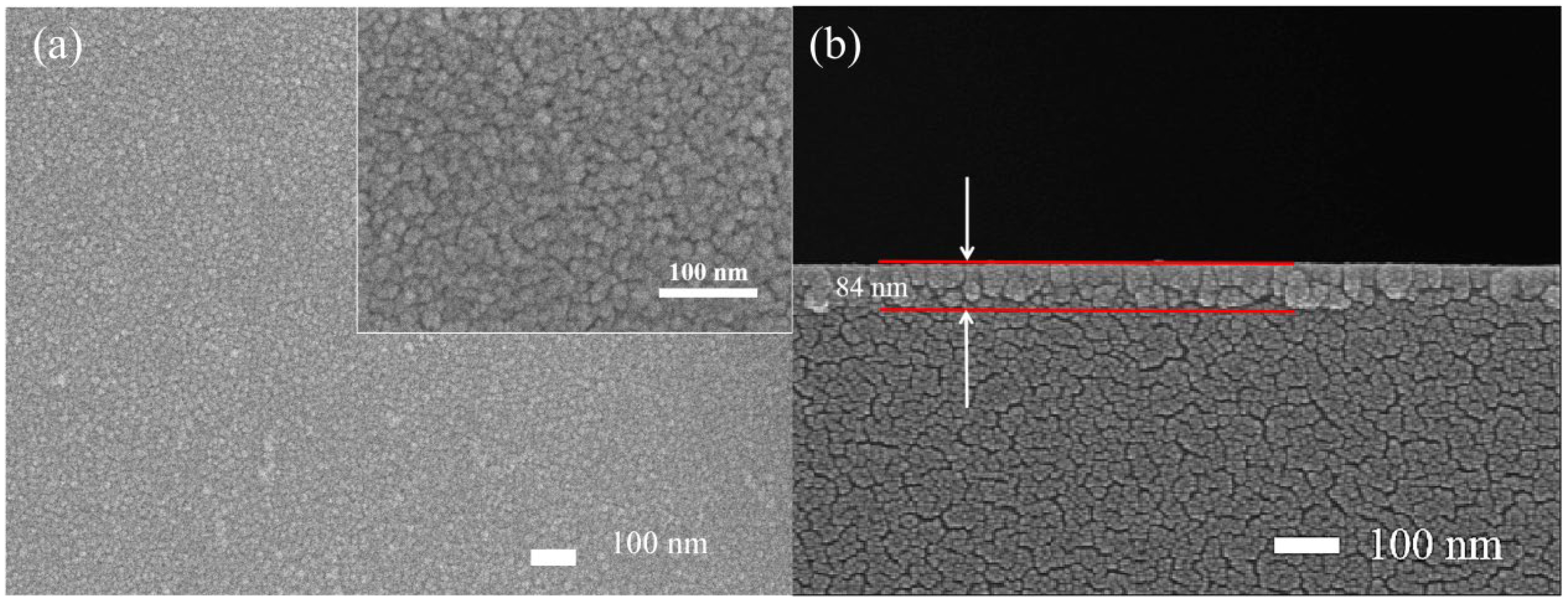
After testing the performance of the prepared UV detectors based on β-Ga2O3, In0.2Ga1.8O3, In0.4Ga1.6O3 and In0.6Ga1.4O3, it was found that the In0.4Ga1.6O3 detector had the best performance. The SEM images of the In0.4Ga1.6O3 film are presented here, and there is no obvious difference among the SEM images of all films. Figure 2a illustrates the top-view scanning electron microscopy (SEM) images of the In0.4Ga1.6O3 film at different magnification scales. Nanoparticles of In0.4Ga1.6O3, with an average diameter of approximately 15 nm, are densely packed on a quartz substrate, forming a compact film. Figure 2b is the cross-view SEM image of the In0.4Ga1.6O3 film. The thickness is about 84 nm. These results indicate the successful preparation of a flat In0.4Ga1.6O3 film.
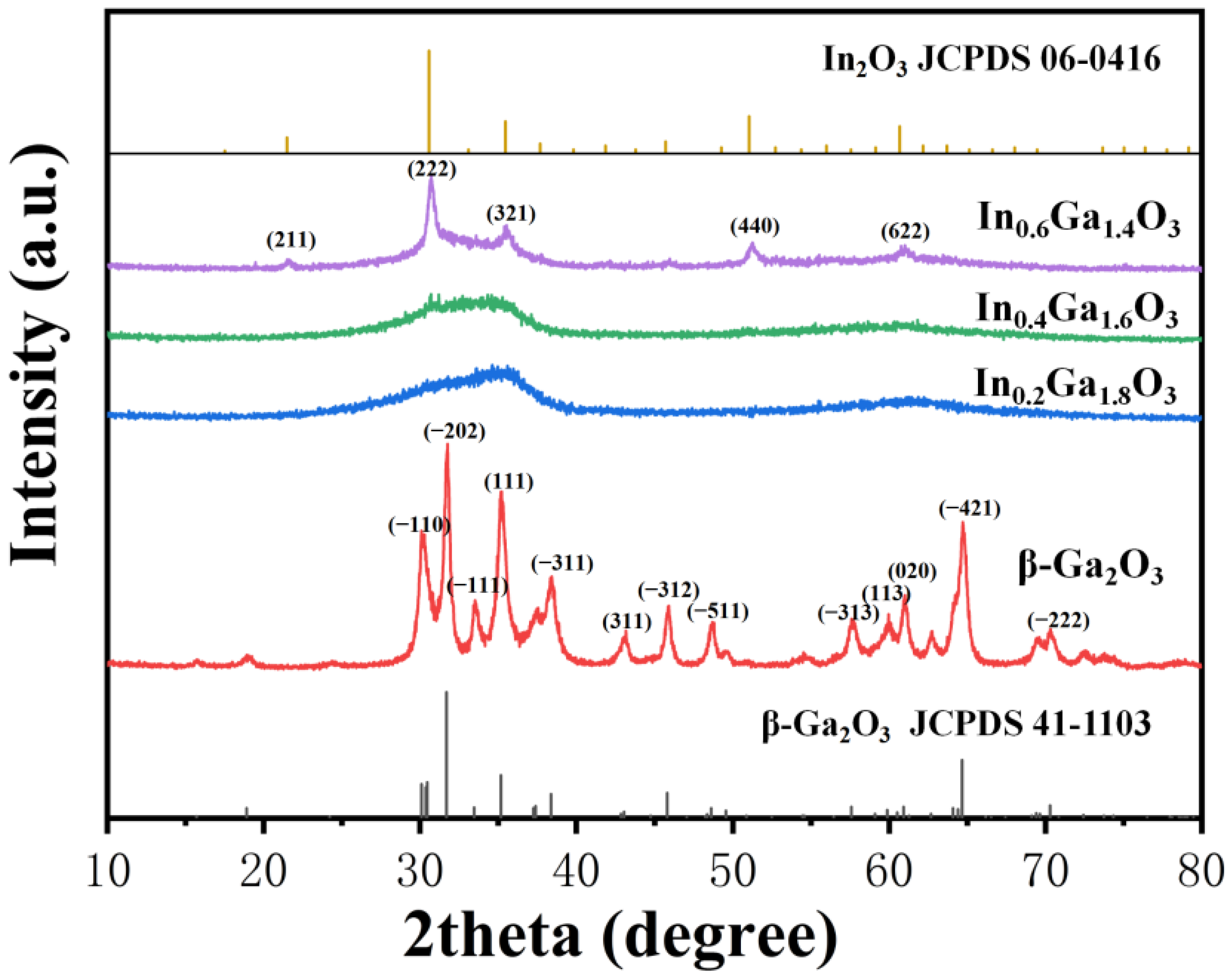
Figure 3 displays the X-ray diffraction patterns of the IGO thin films. The β-Ga2O3 film with an In doping concentration of 0% is crystalline, and the observed (−110), (−202), (111), (−311), (−312) and (−421) main peaks are consistent with the β-Ga2O3 phase, which match well with the JCPDS card number 41-1103 [27]. As the In doping concentration increases, the peak intensities decrease, the full width at half maximum (FWHM) broadens, and the surface crystal quality deteriorates. In the In0.6Ga1.4O3 films, the observed (222), (321), (440), and (622) main peaks are consistent with the In2O3 phase with the JCPDS card number 06-0416 [28]. As the In doping concentration increases from 0% to 30%, a phase transition occurs from the β-Ga2O3 phase to the In2O3 phase [21,29].
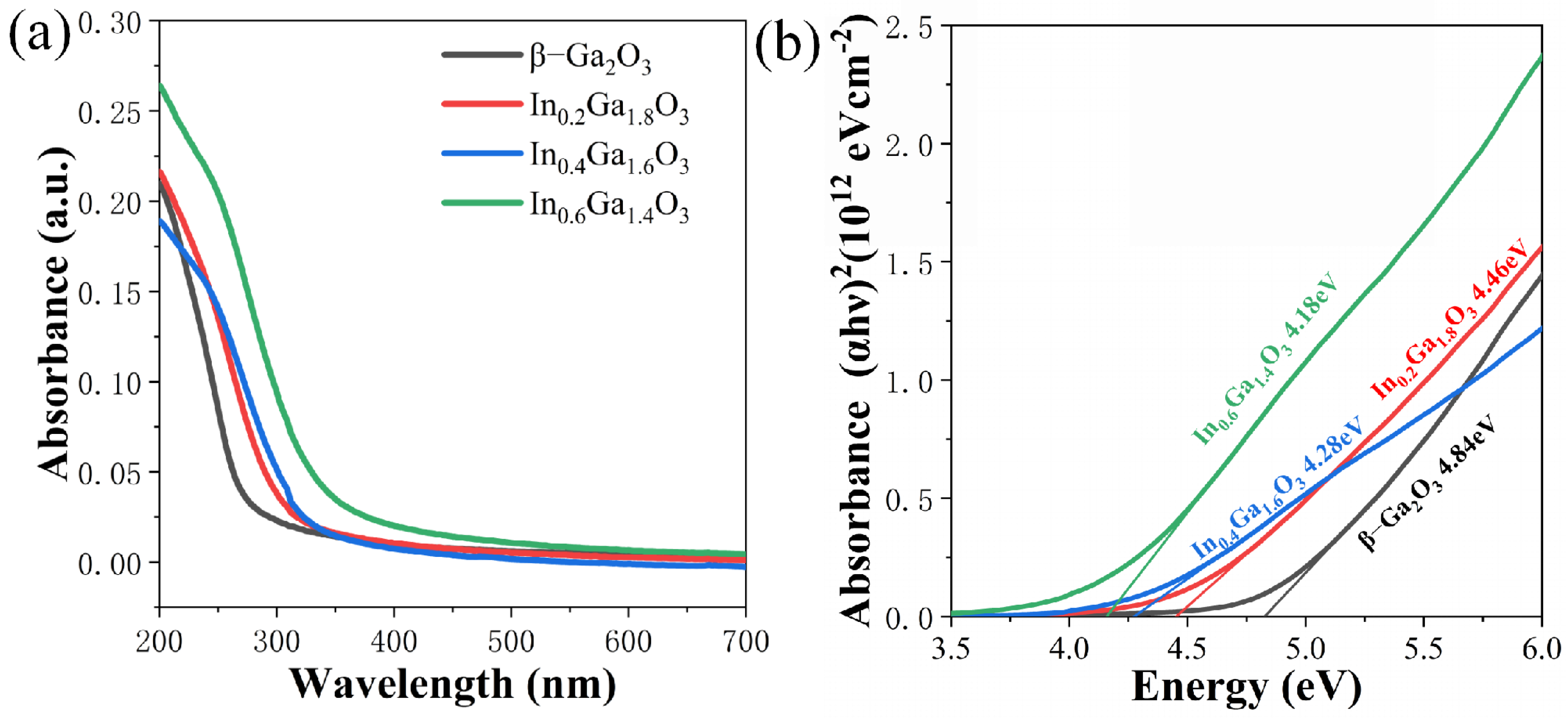
Figure 4a presents the optical absorption spectra of the β-Ga2O3 and IGO films. All films exhibit significant light absorption in the ultraviolet region. As the In content increases, the absorbance of the films increases, indicating enhanced ultraviolet light absorption by the films. Additionally, it can be roughly observed that as the In content increases, the absorption edge of the curve experiences a redshift. The following formula, Tauc equation, is used to calculate the material’s bandgap width based on the absorption spectra, providing a detailed comparison of how the increase in In content affects the material’s bandgap width [30]:
where α is absorption coefficient, A is a constant, h is Planck’s constant, ν is the frequency of the light, Eg is the bandgap energy and the exponent n is denoted as the nature of transitions.
As can be seen from Figure 4b, the approximate bandgap width of the thin film materials continuously decreases with increasing In doping concentration. The energy value of the films decreases progressively, with the β-Ga2O3 film having 4.84 eV, the In0.2Ga1.8O3 film possessing 4.46 eV, the In0.4Ga1.6O3 film exhibiting 4.28 eV, and finally, the In0.6Ga1.4O3 film featuring 4.18 eV, the trend is the same in other researchers’ work [21,26,31].
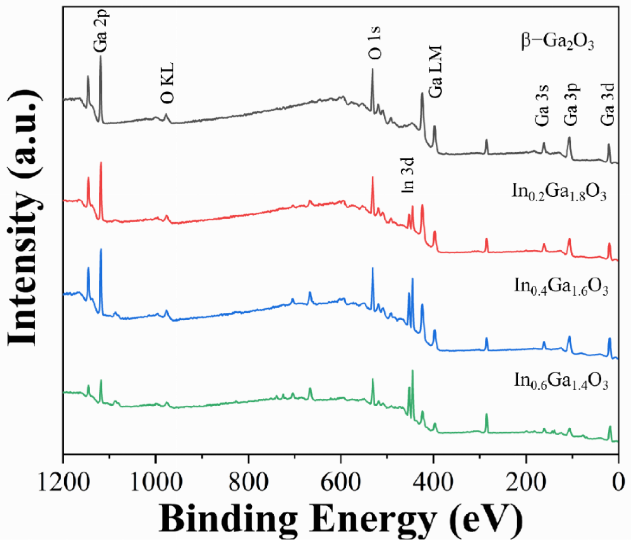
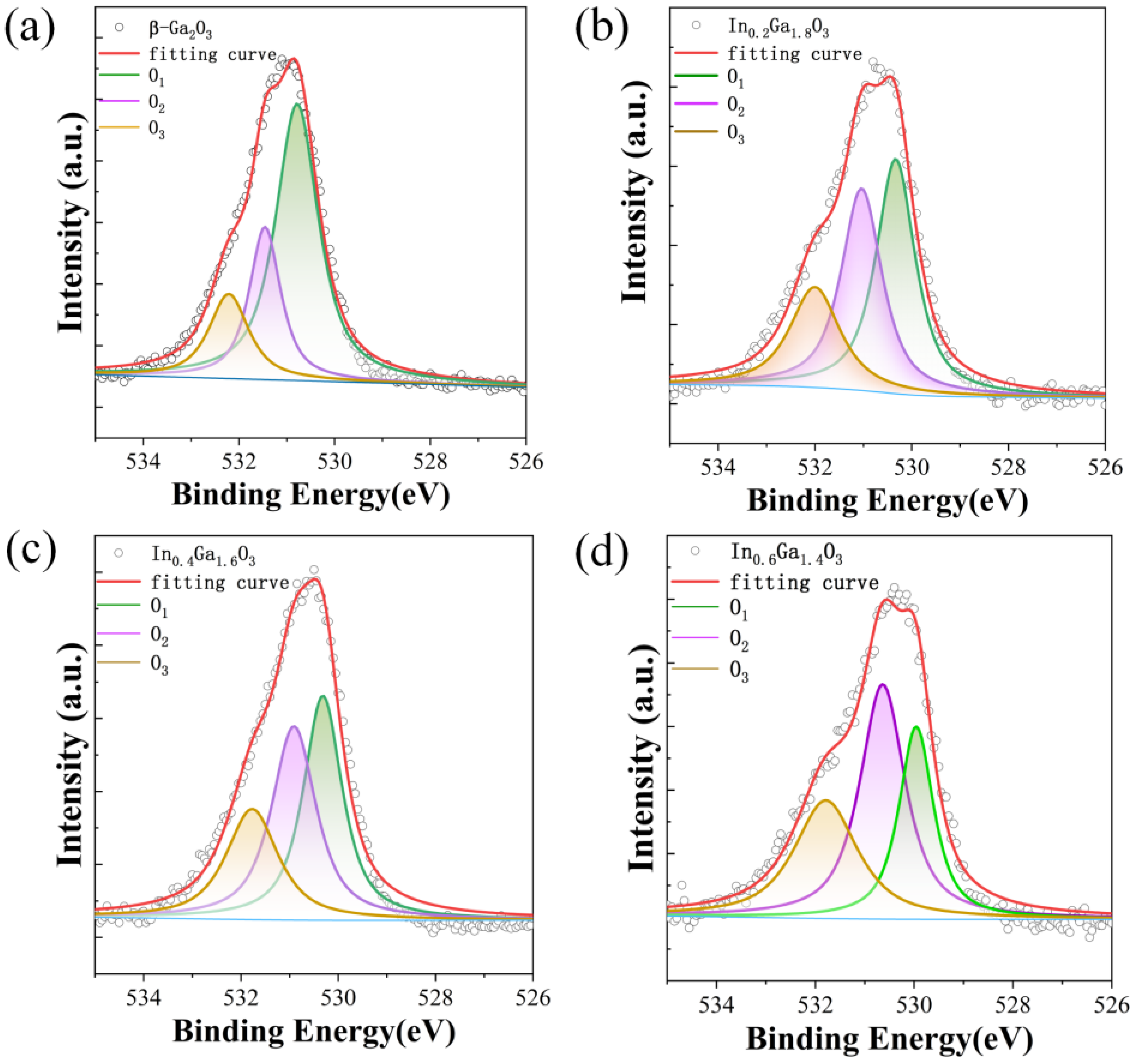
The chemical composition of IGO films was investigated using X-ray photoelectron spectroscopy (XPS). Figure 5 shows the full XPS spectrum, and Figure 6 presents the O1s spectra for the four types of thin films. The actual chemical compositions of the β-Ga2O3, In0.2Ga1.8O3, In0.4Ga1.6O3 and In0.6Ga1.4O3 films are Ga0.2938O0.7062, In0.0747Ga0.2796O0.6457, In0.1256Ga0.2624O0.6124 and In0.2092Ga0.1761O0.6147 from XPS analysis. With In doping, the amount of In increases from 0.0747, 0.1256 to 0.2093, which is approximately equal to 1:2:3. The amount of Ga decreases from 0.2938, 0.2796, 0.2624 to 0.1761, which is approximately equal to 1:0.9:0.8:0.7. To distinguish the XPS measurements, Gaussian fitting was used to divide the typical O1s peak into three peaks. The deconvoluted peak near 530 eV corresponds to lattice oxygen, while the deconvoluted peak near 531 eV corresponds to defect oxygen [21]. The deconvoluted peak near 532 eV corresponds to adsorbed oxygen [32]. By comparing the four thin film devices, it was found that as the In doping concentration increases, the proportion of lattice oxygen decreases, and the proportion of defect oxygen increases. In the O1s spectrum of In0.6Ga1.4O3, the proportion of lattice oxygen is smaller than that of defect oxygen. Combined with the XRD characterization of In0.6Ga1.4O3, it indicates that as the In content increases to a certain extent, In aggregation occurs on the surface of In0.6Ga1.4O3, altering the chemical environment of the material surface.
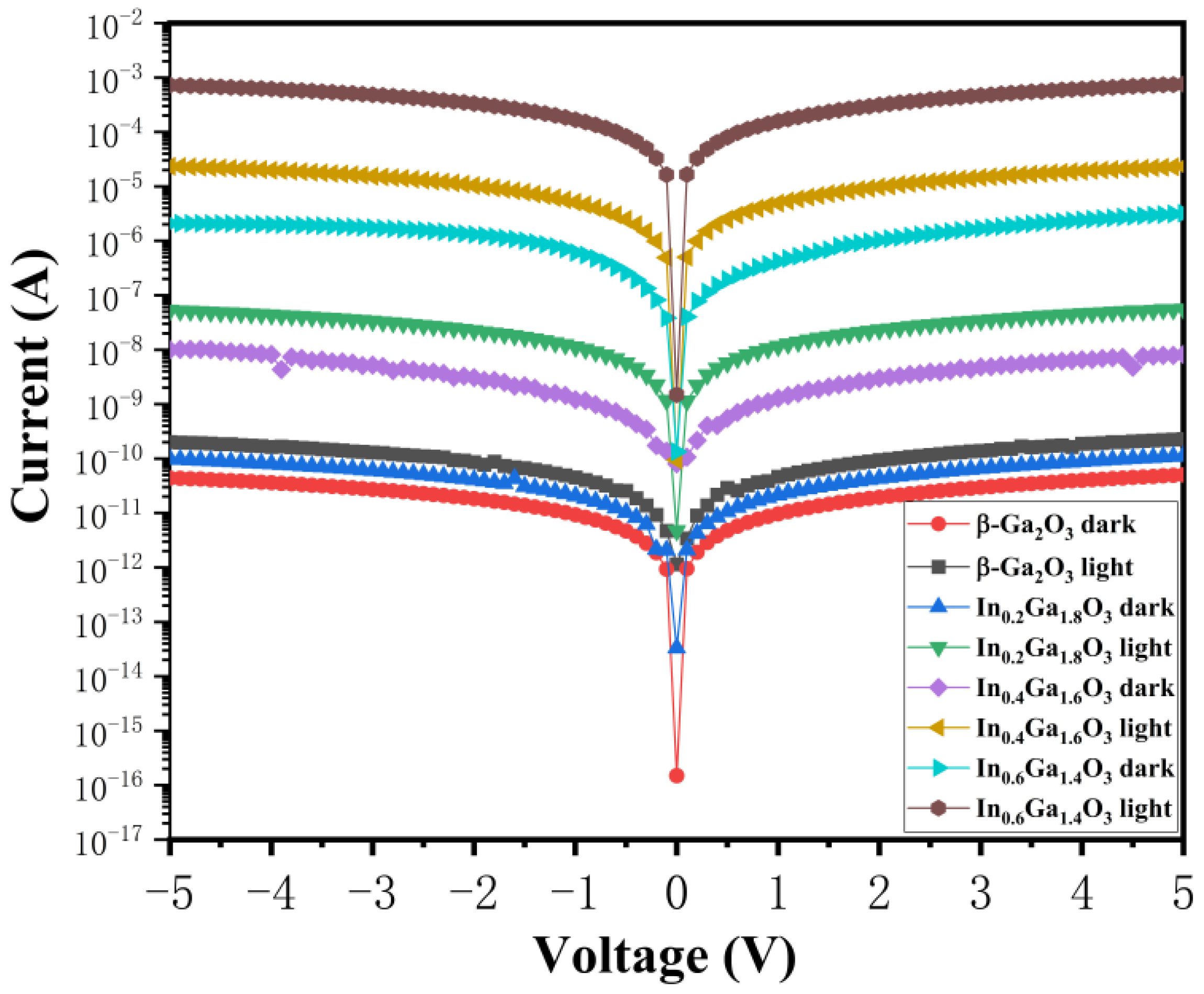
Figure 7 displays the I-V curves of β-Ga2O3 and IGO devices under dark and UV illumination (β-Ga2O3 @260 nm, 4.8 μW/cm2, and IGO @260 and 270 nm, 6.8 and 9.7 μW/cm2) at biases ranging from −5 to 5 V. By comparing the photocurrents of the β-Ga2O3, In0.2Ga1.8O3, In0.4Ga1.6O3, and In0.6Ga1.4O3 devices, it reveals that as the In doping increases, the photocurrent gradually increases, and the increase is quite substantial. At a 5V bias, the photocurrents of the devices with In doping concentrations of 0%, 10%, 20%, and 30% are 0.2 nA, 53.2 nA, 23.4 μA, and 758.5 μA, respectively. It can be observed that as the In doping concentration increases, the rate of increase in the photocurrent of the device slows down. At a 5V bias, the dark currents of the β-Ga2O3, In0.2Ga1.8O3, In0.4Ga1.6O3, and In0.6Ga1.4O3 devices are 0.05 nA, 0.1 nA, 8.2 nA, and 3.0 μA, respectively. It can be seen that as In doping concentration increases, the rate of increase in the dark current of the device accelerates.
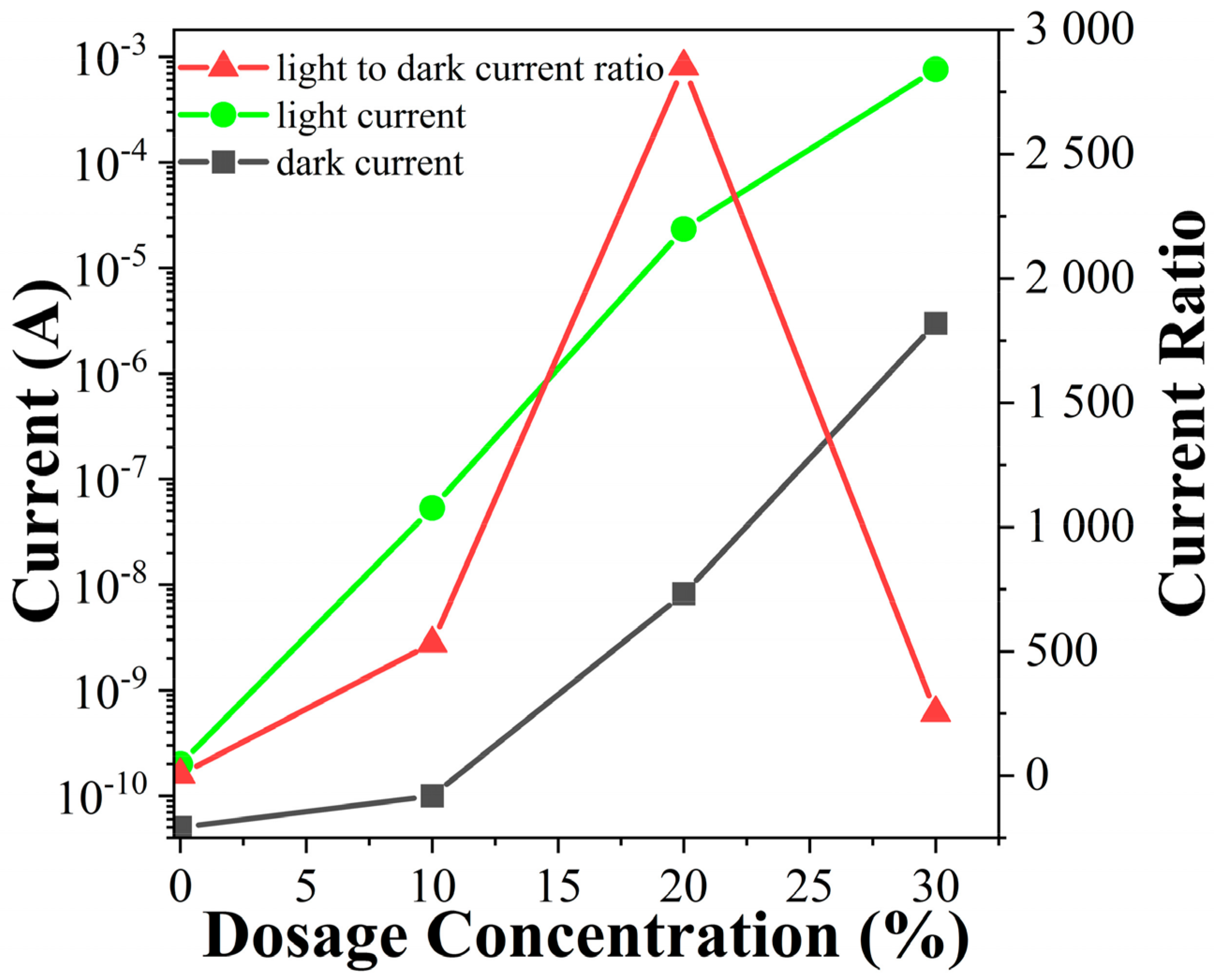
Based on the I-V curves, it was found that as the In doping concentration increases, the photocurrent and dark current of the devices exhibit different rates of increase. To illustrate this trend, Figure 8 shows the light current, dark current, and light-to-dark current ratio of the four devices at a 5V bias. Among them, the In0.4Ga1.6O3 thin film device demonstrates the highest ratio, at 2.8 × 10³, which is an order of magnitude higher than the other two devices.
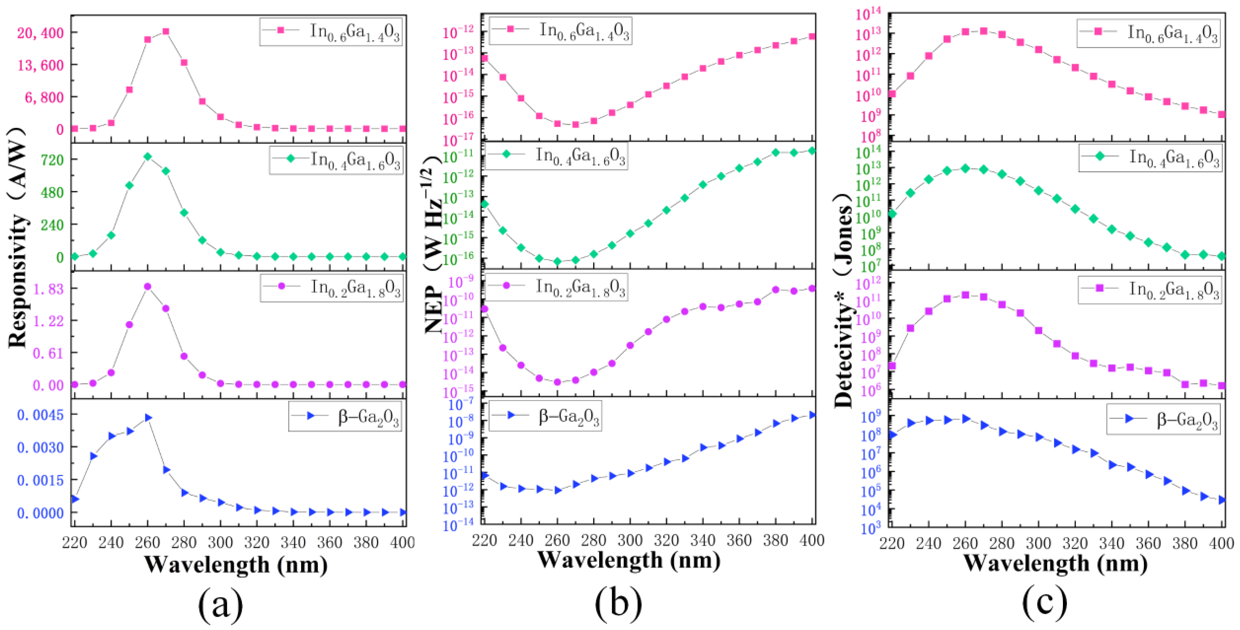
Figure 9a shows the characteristic photoresponse spectra of the photodetector at 5 V bias. The responsivity can be expressed as [33]:
where Iph(λ) and Id(λ) are photocurrent and current in dark, λ is wavelength of light, A and P(λ) are effective area of the devices and luminous power, respectively. Under 260 nm UV light irradiation, the β-Ga2O3, In0.2Ga1.8O3 and In0.4Ga1.6O3 devices achieve their maximum responsivity, at 0.00433 A/W, 1.86 A/W and 739.2 A/W, respectively. Under 270 nm UV light irradiation, the In0.6Ga1.4O3 device reaches its maximum responsivity, at 20,579 A/W. Noise equivalent power (NEP) is defined as the minimum incident radiation power demanded to realize an SNR (signal to noise ratio) of 1 in a 1 Hz bandwidth. NEP can be expressed as [33]:
The main noise of MSM photodetectors is shot noise, so the mean-square noise current can be shot noise, as in Formula (3). NEP is relevant to a low noise signal and a large responsivity. In Figure 9b the NEP of β-Ga2O3, In0.2Ga1.8O3 and In0.4Ga1.6O3 devices are 9.23 × 10⁻¹³ W Hz−1/2, 3.04 × 10⁻¹⁵ W Hz−1/2 and 6.93 × 10⁻¹⁷ W Hz−1/2 at 260 nm, and the NEP of In0.6Ga1.4O3 device is 4.76 × 10⁻¹⁷ W Hz−1/2 at 270 nm. The smaller the NEP is, the better the device’s performance. The detectivity* D* represents the ability to detect weak signals from a noise environment, and is calculated by [33]:
The D* of β-Ga2O3, In0.2Ga1.8O3 and In0.4Ga1.6O3 devices in Figure 9c are 6.68 × 10⁸ Jones, 2.03 × 10¹¹ Jones and 8.89 × 10¹² Jones under 260 nm UV irradiation. The D* of In0.6Ga1.4O3 device is 1.29 × 10¹³ Jones under 270 nm UV irradiation.
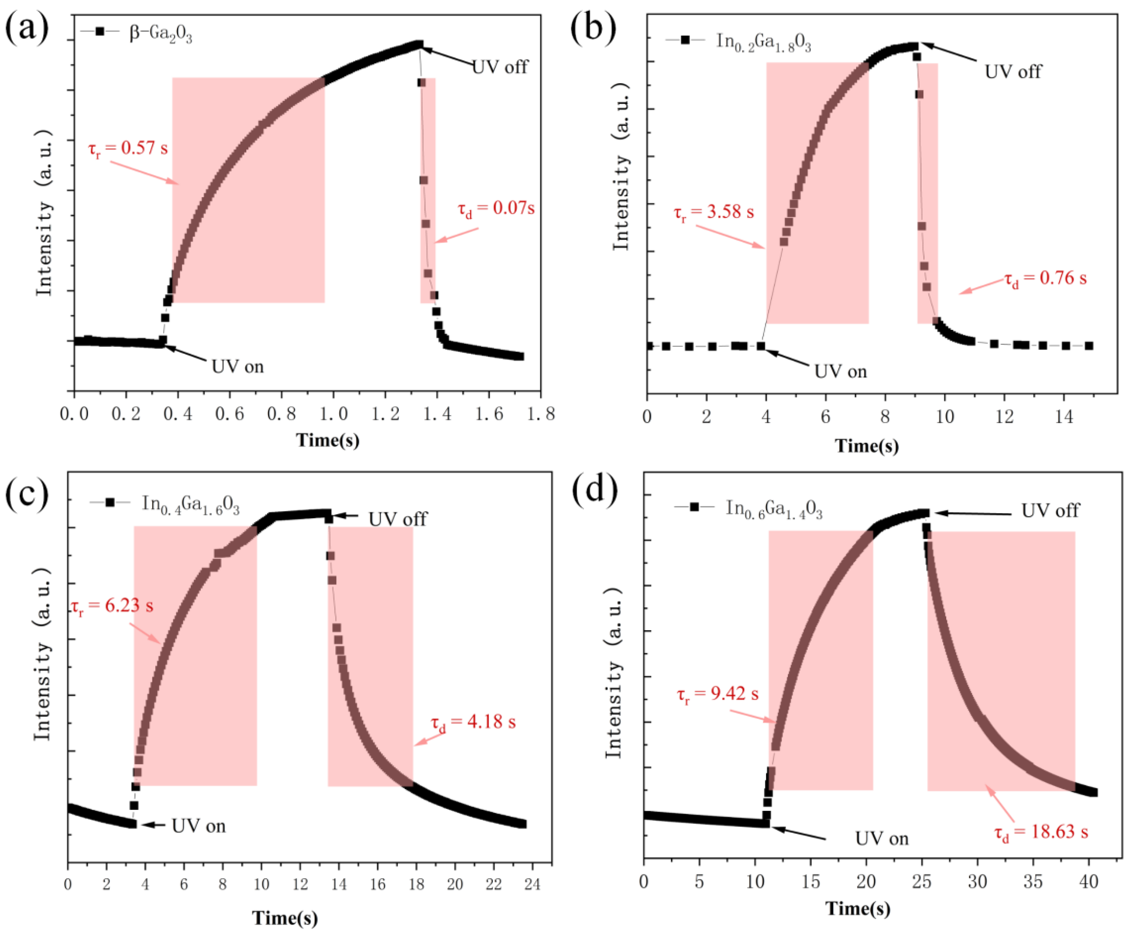
For IGO photodetectors with a 5V bias applied, Figure 10 shows the rise time (τr) and decay time (τd) of the photocurrent. The response times (from 10% to 90% of the total value) for β-Ga2O3, In0.2Ga1.8O3, In0.4Ga1.6O3, and In0.6Ga1.4O3 are 0.57 s, 3.58 s, 6.23 s, and 9.42 s, respectively. The recovery times (from 90% to 10% of the total value) are 0.07 s, 0.76 s, 4.18 s, and 18.63 s. The devices exhibit such time response characteristics mainly due to the conduction mechanism of oxygen vacancies. The undoped β-Ga2O3 thin film device has high crystalline quality and fewer oxygen vacancies, allowing electron-hole pairs to recombine rapidly. In the In-doped thin film devices, the presence of an additional electron layer of the In element compared to the Ga element results in a larger ionic radius, which hinders the crystal growth process of β-Ga2O3, leading to an amorphous appearance and the generation of more oxygen vacancy defects [34,35]. Therefore, the response and recovery times of the devices increase significantly in thin film devices with different In doping concentrations. The higher the In doping concentration, the more oxygen vacancies are generated, and the longer the response and recovery times of the thin film devices are.
Table 1 is a summary of the parameters of β-Ga2O3, In0.2Ga1.8O3, In0.4Ga1.6O3, and In0.6Ga1.4O3 MSM UV photodetectors.
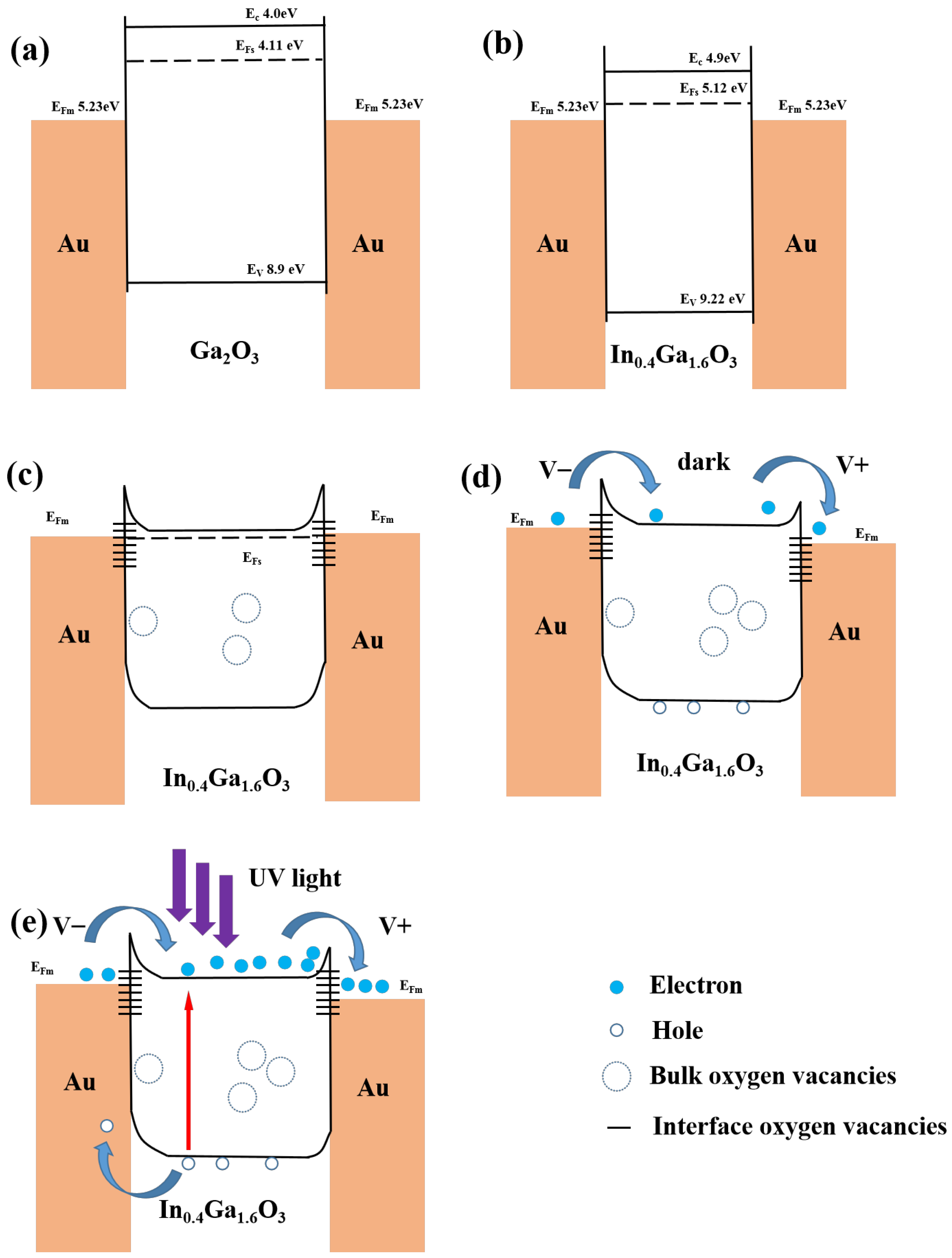
Figure 11 shows the energy band diagram to explain the overall mechanism. Now we discuss the main cases of the In0.4Ga1.6O3 MSM structure. Before contact in Figure 11a,b, the work function of Au is 5.23 eV, and the work functions of β-Ga2O3 and In0.4Ga1.6O3 are 4.11 eV and 5.12 eV, respectively, which are both higher than those of Au, and thus forming Schottky contacts. The electron affinities of β-Ga2O3 and In0.4Ga1.6O3 are 4.11 eV and 4.9 eV, and the two bandgaps are 4.9 eV and 4.3 eV. Both β-Ga2O3 and In2O3 are n-type semiconductors, and the bandgap of In2O3 is 3.67 eV. With In doping into β-Ga2O3, the bandgap becomes small and the Fermi level changes from 4.11 eV to 5.12 eV [36,37]. Furthermore, with increasingly higher In doping concentrations, a larger number of oxygen vacancies capture holes, leading to an augmentation of electron transition density [38]. These interface oxygen vacancies contribute to the interface state, which leads to a decrease in the Schottky barrier. After contact with no bias in Figure 11c, there are bulk oxygen vacancies and interface oxygen vacancies in Au/In0.4Ga1.6O3/Au, and the spikes form when both Fermi levels are unified. When a certain bias is applied on the MSM structure, there is always a reverse Schottky diode. Electrons will cross the barrier under bias, in the way of hot electron emission and tunneling, which forms the dark current, as is shown in Figure 11d. The Fermi level of Au in two reverse Schottky junctions will differ with electrons flowing under bias. Under UV light and a certain bias in Figure 11e, photogenerated electron-hole pairs will be separated by the built-in electrical field of Au and In0.4Ga1.6O3, which contributes to the accumulation of carries and thus improves the photocurrent [39]. As the In doping concentration increases from 10% to 20%, the amorphous state of the film increases. The significant increase in photocurrent is mainly attributed to the increase in the density of electron transitions within the film, while the enhancement of the light-to-dark current ratio is attributed to the pronounced increase in photocurrent [40,41]. With the In doping content rising from 20% to 30%, the film transforms from an amorphous state to the In2O3 phase. The significant increase in dark current of the device is mainly attributed to the increase in electron mobility (bulk oxygen vacancies by In doping) and the narrowing of the Schottky barrier (interface state by interface oxygen vacancies) due to the formation of the In2O3 phase [42]. The decrease in the light-to-dark current ratio of the device is attributed to the significant increase in dark current. Since the growth rates of photocurrent and dark current are inconsistent, the device with an In doping concentration of 20% has the highest photocurrent-to-dark current suppression ratio.
Table 2 is the performances compared with other GaO-alloy MSM UV photodetectors, which differ among various element compositions and proportions. The In0.4Ga1.6O3 MSM UV photodetector in this work has a relatively high light current, photo to dark current ratio and responsivity, which indicates the In0.4Ga1.6O3 material having a promising future in UV detection.
4. Conclusions
In summary, the effects of indium (In) content on IGO thin-film photodetectors were investigated. As the In doping concentration increased, the thin film transitioned from the β-Ga2O3 phase to amorphous phase, and then to the In2O3 phase. A device that exhibits high responsivity (739.2 A/W) and a high photocurrent-to-dark-current suppression ratio (2.8 × 10³) was prepared by utilizing the In0.4Ga1.6O3 thin film, which is in the intermediate phase transition process. Furthermore, the influence of Schottky barriers and oxygen vacancies on photocurrent and dark current was explored. Devices with superior performance and greater application potential can be developed by improving traditional single-layer devices through elemental doping.
Author Contributions
All authors contributed to the design and development of the experiments, the implementation and the writing of the paper. Specifically, conceptualization, R.Z. and Z.B.; methodology, Z.B.; software, C.L.; validation, X.L. (Xin Li); formal analysis, X.L. (Xin Li); investigation, Y.Z. and R.Z.; resources, X.L. (Xinyan Liu) and Y.C.; data curation, X.L. (Xinyan Liu) and Y.M.; writing—original draft preparation, Y.Z.; writing—review and editing, S.R. and J.Z.; visualization, Y.M.; supervision, Y.C.; project administration, R.Z.; funding acquisition, S.R. All authors have read and agreed to the published version of the manuscript.
Funding
This research was funded by National Natural Science Foundation of China (Grant No. 12073009, 61974055, U21B2061, 12374397), Project of Science and Technology Plan of Jilin Province (Grant No. 20210301010GX) for the support to this work.
Institutional Review Board Statement
Not applicable.
Informed Consent Statement
Not applicable.
Data Availability Statement
The data presented in this study are available on request from the corresponding author.
Conflicts of Interest
The authors declare no conflict of interest.
References
- Pearton, S.J.; Yang, J.; Cary, P.H.; Ren, F.; Kim, J.; Tadjer, M.J.; Mastro, M.A. A review of Ga2O3 materials, processing, and devices. Appl. Phys. Rev. 2018, 5, 011301. [Google Scholar] [CrossRef]
- Wu, C.; Wu, F.; Ma, C.; Li, S.; Liu, A.; Yang, X.; Chen, Y.; Wang, J.; Guo, D. A general strategy to ultrasensitive Ga2O3 based self-powered solar-blind photodetectors. Mater. Today Phys. 2022, 23, 100643. [Google Scholar] [CrossRef]
- Yu, J.; Tian, N.; Deng, Y.F.; Zhang, H.H. Ultraviolet photodetector based on sol-gel synthesized MgZnO nanoparticle with photoconductive gain. J. Alloys Compd. 2016, 667, 359–362. [Google Scholar] [CrossRef]
- Yu, R.X.; Liu, G.X.; Wang, G.D.; Chen, C.M.; Xu, M.S.; Zhou, H.; Wang, T.L.; Yu, J.X.; Zhao, G.; Zhang, L. Ultrawide-bandgap semiconductor AlN crystals: Growth and applications. J. Mater. Chem. C 2021, 9, 1852–1873. [Google Scholar] [CrossRef]
- Xu, Y.; Chen, X.; Zhou, D.; Ren, F.; Zhou, J.; Bai, S.; Lu, H.; Gu, S.; Zhang, R.; Zheng, Y.; et al. Carrier Transport and Gain Mechanisms in beta-Ga2O3-Based Metal-Semiconductor-Metal Solar-Blind Schottky Photodetectors. IEEE Trans. Electron Devices 2019, 66, 2276–2281. [Google Scholar] [CrossRef]
- Shen, H.; Yin, Y.; Tian, K.; Baskaran, K.; Duan, L.; Zhao, X.; Tiwari, A. Growth and characterization of β-Ga2O3 thin films by sol-gel method for fast-response solar-blind ultraviolet photodetectors. J. Alloys Compd. 2018, 766, 601–608. [Google Scholar] [CrossRef]
- Guo, D.Y.; Qin, X.Y.; Lv, M.; Shi, H.Z.; Su, Y.L.; Yao, G.S.; Wang, S.L.; Li, C.R.; Li, P.G.; Tang, W.H. Decrease of oxygen vacancy by Zn-doped for improving solar-blind photoelectric performance in beta-Ga2O3 thin films. Electron. Mater. Lett. 2017, 13, 483–488. [Google Scholar] [CrossRef]
- Liang, H.L.; Cui, S.J.; Su, R.; Guan, P.F.; He, Y.H.; Yang, L.H.; Chen, L.M.; Zhang, Y.H.; Mei, Z.X.; Du, X.L. Flexible X-ray Detectors Based on Amorphous Ga2O3 Thin Films. ACS Photonics 2019, 6, 351–359. [Google Scholar] [CrossRef]
- Ouyang, W.X.; Teng, F.; Jiang, M.M.; Fang, X.S. ZnO Film UV Photodetector with Enhanced Performance: Heterojunction with CdMoO4 Microplates and the Hot Electron Injection Effect of Au Nanoparticles. Small 2017, 13, 1702177. [Google Scholar] [CrossRef]
- Teng, F.; Ouyang, W.X.; Li, Y.M.; Zheng, L.X.; Fang, X.S. Novel Structure for High Performance UV Photodetector Based on BiOCl/ZnO Hybrid Film. Small 2017, 13, 1700156. [Google Scholar] [CrossRef]
- Wang, F.X.; Wang, Z.; Fan, S.Y.; Li, M. The effect of structural parameters on AlGaN solar-blind metal-semiconductor-metal (MSM) photodetectors. Opt. Quantum Electron. 2021, 53, 671. [Google Scholar] [CrossRef]
- Kim, K.P.; Chang, D.; Lim, S.K.; Lee, S.K.; Lyu, H.K.; Hwang, D.K. Thermal annealing effects on the dynamic photoresponse properties of Al-doped ZnO nanowires network. Curr. Appl. Phys. 2011, 11, 1311–1314. [Google Scholar] [CrossRef]
- Shabannia, R. High-sensitivity UV photodetector based on oblique and vertical Co-doped ZnO nanorods. Mater. Lett. 2018, 214, 254–256. [Google Scholar] [CrossRef]
- Shabannia, R.; Naderi, N. High UV-to-Visible Rejection Ratio and Low Cost UV Photodetector Based on Co-Doped ZnO Nanorods Grown on Polyethylene Terephthalate Substrate. J. Nanoelectron. Optoelectron. 2019, 14, 1368–1373. [Google Scholar] [CrossRef]
- Young, S.J.; Liu, Y.H. Low-frequency noise properties of MgZnO nanorod ultraviolet photodetectors with and without UV illumination. Sens. Actuators A Phys. 2018, 269, 363–368. [Google Scholar] [CrossRef]
- Dai, W.; Pan, X.H.; Chen, S.S.; Chen, C.; Chen, W.; Zhang, H.H.; Ye, Z.Z. ZnO homojunction UV photodetector based on solution-grown Sb-doped p-type ZnO nanorods and pure n-type ZnO nanorods. RSC Adv. 2014, 5, 6311–6314. [Google Scholar] [CrossRef]
- Raj, I.L.P.; Valanarasu, S.; Vinoth, S.; Chidhambaram, N.; Isaac, R.S.R.; Ubaidullah, M.; Shaikh, S.F.; Pandit, B. Highly sensitive ultraviolet photodetectors fabricated from rare earth metal ions doped NiO thin films via nebulizer spray pyrolysis method. Sens. Actuators A Phys. 2021, 333, 113242. [Google Scholar] [CrossRef]
- Rajamanickam, S.; Mohammad, S.M.; Razak, I.A.; Muhammad, A.; Abed, S.M. Enhanced sensitivity from Ag micro-flakes encapsulated Ag-doped ZnO nanorods-based UV photodetector. Mater. Res. Bull. 2023, 161, 112148. [Google Scholar] [CrossRef]
- Yadav, P.V.K.; Ajitha, B.; Ahmed, C.M.A.; Reddy, Y.A.K.; Reddy, V.R.M. Superior UV photodetector performance of TiO2 films using Nb doping. J. Phys. Chem. Solids 2021, 160, 110350. [Google Scholar] [CrossRef]
- Zhang, Y.F.; Liu, X.Y.; Yan, L.M.; Xu, R.L.; Chen, Y.; Zhou, J.R.; Ruan, S.P. Ytterbium doping reduces the dark current of UV photoelectric detector based on TiO2. Mater. Chem. Phys. 2023, 293, 126966. [Google Scholar] [CrossRef]
- Swallow, J.E.N.; Palgrave, R.G.; Murgatroyd, P.A.E.; Regoutz, A.; Lorenz, M.; Hassa, A.; Grundmann, M.; von Wenckstern, H.; Varley, J.B.; Veal, T.D. Indium Gallium Oxide Alloys: Electronic Structure, Optical Gap, Surface Space Charge, and Chemical Trends within Common-Cation Semiconductors. ACS Appl. Mater. Interfaces 2021, 13, 2807–2819. [Google Scholar] [CrossRef] [PubMed]
- Zhang, J.Y.; Shi, J.L.; Qi, D.C.; Chen, L.; Zhang, K.H.L. Recent progress on the electronic structure, defect, and doping properties of Ga2O3. APL Mater. 2020, 8, 020906. [Google Scholar] [CrossRef]
- Chang, S.-P.; Chang, L.-Y.; Li, J.-Y. The Influence of Different Partial Pressure on the Fabrication of InGaO Ultraviolet Photodetectors. Sensors 2016, 16, 2145. [Google Scholar] [CrossRef] [PubMed]
- Kokubun, Y.; Abe, T.; Nakagomi, S. Sol-gel prepared (Ga1−xInx)2O3 thin films for solar-blind ultraviolet photodetectors. Phys. Status Solidi A-Appl. Mater. Sci. 2010, 207, 1741–1745. [Google Scholar] [CrossRef]
- Chen, K.-Y.; Hsu, C.-C.; Yu, H.-C.; Peng, Y.-M.; Yang, C.-C.; Su, Y.-K. The Effect of Oxygen Vacancy Concentration on Indium Gallium Oxide Solar Blind Photodetector. IEEE Trans. Electron Devices 2018, 65, 1817–1822. [Google Scholar] [CrossRef]
- Hatipoglu, I.; Mukhopadhyay, P.; Alema, F.; Sakthivel, T.S.; Seal, S.; Osinsky, A.; Schoenfeld, W.V. Tuning the responsivity of monoclinic (InxGa1−x)2O3 solar-blind photodetectors grown by metal organic chemical vapor deposition. J. Phys. D Appl. Phys. 2020, 53, 454001. [Google Scholar] [CrossRef]
- Nakagomi, S.; Kokubun, Y. Crystal orientation of beta-Ga2O3 thin films formed on c-plane and a-plane sapphire substrate. J. Cryst. Growth 2012, 349, 12–18. [Google Scholar] [CrossRef]
- Zhang, M.X.; Yu, H.; Li, H.; Jiang, Y.; Qu, L.H.; Wang, Y.X.; Gao, F.; Feng, W. Ultrathin In2O3 Nanosheets toward High Responsivity and Rejection Ratio Visible-Blind UV Photodetection. Small 2023, 19, 2205623. [Google Scholar] [CrossRef]
- Wouters, C.; Sutton, C.; Ghiringhelli, L.M.; Markurt, T.; Schewski, R.; Hassa, A.; von Wenckstern, H.; Grundmann, M.; Scheffler, M.; Albrecht, M. Investigating the ranges of (meta)stable phase formation in (InxGa1−x)2O3: Impact of the cation coordination. Phys. Rev. Mater. 2020, 4, 125001. [Google Scholar] [CrossRef]
- Lee, C.T.; Liu, Y.H.; Lee, H.Y. Stacked Triple Ultraviolet-Band Metal-Semiconductor-Metal Photodetectors. IEEE Photonics Technol. Lett. 2019, 31, 15–18. [Google Scholar] [CrossRef]
- Peelaers, H.; Steiauf, D.; Varley, J.B.; Janotti, A.; Van de Walle, C.G. (InxGa1−x)2O3 alloys for transparent electronics. Phys. Rev. B 2015, 92, 085206. [Google Scholar] [CrossRef]
- Remashan, K.; Hwang, D.K.; Park, S.D.; Bae, J.W.; Yeom, G.Y.; Park, S.J.; Jang, J.H. Effect of N2O plasma treatment on the performance of ZnO TFTs. Electrochem. Solid-State Lett. 2008, 11, H55–H59. [Google Scholar] [CrossRef]
- Wang, F.; Wang, Z.X.; Yin, L.; Cheng, R.Q.; Wang, J.J.; Wen, Y.; Shifa, T.A.; Wang, F.M.; Zhang, Y.; Zhan, X.Y.; et al. 2D library beyond graphene and transition metal dichalcogenides: A focus on photodetection. Chem. Soc. Rev. 2018, 47, 6296–6341. [Google Scholar] [CrossRef]
- Kneiss, M.; Hassa, A.; Splith, D.; Sturm, C.; von Wenckstern, H.; Lorenz, M.; Grundmann, M. Epitaxial stabilization of single phase κ-(InxGa1−x)2O3 thin films up to x = 0.28 on c-sapphire and κ-Ga2O3(001) templates by tin-assisted VCCS-PLD. APL Mater. 2019, 7, 101102. [Google Scholar] [CrossRef]
- von Wenckstern, H.; Splith, D.; Werner, A.; Müller, S.; Lorenz, M.; Grundmann, M. Properties of Schottky Barrier Diodes on (InxGa1−x)2O3 for 0.01 ≤ x ≤ 0.85 Determined by a Combinatorial Approach. ACS Comb. Sci. 2015, 17, 710–715. [Google Scholar] [CrossRef] [PubMed]
- Bi, Z.; Zhang, Y.; Zhang, Y.; Liu, X.; Ma, Y.; Li, X.; Liu, C.; Chen, Y.; Zhou, J.; Ruan, S. MSM UV photodetector with low dark current based on GaInO/SrTiO3 heterojunction. Mater. Sci. Semicond. Process. 2024, 170, 107973. [Google Scholar] [CrossRef]
- Mohamed, M.; Irmscher, K.; Janowitz, C.; Galazka, Z.; Manzke, R.; Fornari, R. Schottky barrier height of Au on the transparent semiconducting oxide β-Ga2O3. Appl. Phys. Lett. 2012, 101, 132106. [Google Scholar] [CrossRef]
- Ryu, B.; Noh, H.-K.; Choi, E.-A.; Chang, K.J. O-vacancy as the origin of negative bias illumination stress instability in amorphous In-Ga-Zn-O thin film transistors. Appl. Phys. Lett. 2010, 97, 022108. [Google Scholar] [CrossRef]
- Guo, D.Y.; Wu, Z.P.; An, Y.H.; Guo, X.C.; Chu, X.L.; Sun, C.L.; Li, L.H.; Li, P.G.; Tang, W.H. Oxygen vacancy tuned Ohmic-Schottky conversion for enhanced performance in β-Ga2O3 solar-blind ultraviolet photodetectors. Appl. Phys. Lett. 2014, 105, 023507. [Google Scholar] [CrossRef]
- Feng, P.; Monch, I.; Harazim, S.; Huang, G.S.; Mei, Y.F.; Schmidt, O.G. Giant Persistent Photoconductivity in Rough Silicon Nanomembranes. Nano Lett. 2009, 9, 3453–3459. [Google Scholar] [CrossRef] [PubMed]
- Xing, W.D.; Kung, S.C.; van der Veer, W.E.; Yan, W.B.; Ayvazian, T.; Kim, J.Y.; Penner, R.M. High-Throughput Fabrication of Photoconductors with High Detectivity, Photosensitivity, and Bandwidth. ACS Nano 2012, 6, 5627–5634. [Google Scholar] [CrossRef] [PubMed]
- Li, C.; Bando, Y.; Liao, M.; Koide, Y.; Golberg, D. Visible-blind deep-ultraviolet Schottky photodetector with a photocurrent gain based on individual Zn2GeO4 nanowire. Appl. Phys. Lett. 2010, 97, 161102. [Google Scholar] [CrossRef]
- Chang, T.H.; Chang, S.J.; Weng, W.Y.; Chiu, C.J.; Wei, C.Y. Amorphous Indium-Gallium-Oxide UV Photodetectors. IEEE Photonics Technol. Lett. 2015, 27, 2083–2086. [Google Scholar] [CrossRef]
- Ma, M.; Zhang, D.; Li, Y.; Lin, R.; Zheng, W.; Huang, F. High-Performance Solar Blind Ultraviolet Photodetector Based on Single Crystal Orientation Mg-Alloyed Ga2O3 Film Grown by a Nonequilibrium MOCVD Scheme. ACS Appl. Electron. Mater. 2019, 1, 1653–1659. [Google Scholar] [CrossRef]
- Zhao, X.; Wu, Z.; Guo, D.; Cui, W.; Li, P.; An, Y.; Li, L.; Tang, W. Growth and characterization of alpha-phase Ga2−xSnxO3 thin films for solar-blind ultraviolet applications. Semicond. Sci. Technol. 2016, 31, 065010. [Google Scholar] [CrossRef]
Figure 1.
Schematic structure of a metal-semiconductor-metal (MSM) photodetector.

Figure 2.
(a) Top-view SEM image of the In0.4Ga1.6O3 film, the inset is the high magnification. (b) Cross-view SEM image of the In0.4Ga1.6O3 film.
Figure 2.
(a) Top-view SEM image of the In0.4Ga1.6O3 film, the inset is the high magnification. (b) Cross-view SEM image of the In0.4Ga1.6O3 film.

Figure 3.
XRD pattern of the β-Ga2O3,In0.2Ga1.8O3,In0.4Ga1.6O3 and In0.6Ga1.4O3 films.

Figure 4.
(a) Absorbance spectra of β-Ga2O3, In0.2Ga1.8O3, In0.4Ga1.6O3 and In0.6Ga1.4O3 films. (b) Bandgap widths of β-Ga2O3, In0.2Ga1.8O3, In0.4Ga1.6O3, and In0.6Ga1.4O3 films.
Figure 4.
(a) Absorbance spectra of β-Ga2O3, In0.2Ga1.8O3, In0.4Ga1.6O3 and In0.6Ga1.4O3 films. (b) Bandgap widths of β-Ga2O3, In0.2Ga1.8O3, In0.4Ga1.6O3, and In0.6Ga1.4O3 films.

Figure 5.
Survey spectra of β-Ga2O3, In0.2Ga1.8O3, In0.4Ga1.6O3, and In0.6Ga1.4O3 films.

Figure 6.
X-ray photoelectron spectroscopy (XPS) spectra of O1s of (a) β-Ga2O3, (b) In0.2Ga1.8O3, (c) In0.4Ga1.6O3, and (d) In0.6Ga1.4O3 films.
Figure 6.
X-ray photoelectron spectroscopy (XPS) spectra of O1s of (a) β-Ga2O3, (b) In0.2Ga1.8O3, (c) In0.4Ga1.6O3, and (d) In0.6Ga1.4O3 films.

Figure 7.
I-V characteristics of β-Ga2O3 and IGO devices under dark and UV illumination.

Figure 8.
The Il, Id and Il to Id ratio values of devices with different In dosage concentration under 5 V bias.
Figure 8.
The Il, Id and Il to Id ratio values of devices with different In dosage concentration under 5 V bias.

Figure 9.
(a) Spectral responsivity (b) NEP (c) Spectral Detectivity* of the β-Ga2O3 and IGO devices at 5 V bias.
Figure 9.
(a) Spectral responsivity (b) NEP (c) Spectral Detectivity* of the β-Ga2O3 and IGO devices at 5 V bias.

Figure 10.
Time response characteristics of (a) β-Ga2O3; (b) In0.2Ga1.8O3; (c) In0.4Ga1.6O3 and (d) In0.6Ga1.4O3 devices.
Figure 10.
Time response characteristics of (a) β-Ga2O3; (b) In0.2Ga1.8O3; (c) In0.4Ga1.6O3 and (d) In0.6Ga1.4O3 devices.

Figure 11.
Schematic energy band diagrams of MSM structure. (a) Au/Ga2O3/Au before contact; (b) Au/In0.4Ga1.6O3/Au before contact; (c) Au/In0.4Ga1.6O3/Au after contact without bias; (d) Au/In0.4Ga1.6O3/Au with bias in dark; (e) Au/In0.4Ga1.6O3/Au with bias under UV light.
Figure 11.
Schematic energy band diagrams of MSM structure. (a) Au/Ga2O3/Au before contact; (b) Au/In0.4Ga1.6O3/Au before contact; (c) Au/In0.4Ga1.6O3/Au after contact without bias; (d) Au/In0.4Ga1.6O3/Au with bias in dark; (e) Au/In0.4Ga1.6O3/Au with bias under UV light.


Table 1.
A summary of the parameters of β-Ga2O3, In0.2Ga1.8O3, In0.4Ga1.6O3, and In0.6Ga1.4O3 photodetectors.
Table 1.
A summary of the parameters of β-Ga2O3, In0.2Ga1.8O3, In0.4Ga1.6O3, and In0.6Ga1.4O3 photodetectors.
| β-Ga2O3 | In0.2Ga1.8O3 | In0.4Ga1.6O3 | In0.6Ga1.4O3 | |
|---|---|---|---|---|
| Eg (eV) | 4.84 | 4.46 | 4.28 | 4.18 |
| Ilight (A) | 2.0 × 10⁻¹⁰ | 5.32 × 10⁻⁸ | 2.34 × 10⁻⁵ | 7.59 × 10⁻⁴ |
| Idark (A) | 5.1 × 10⁻¹¹ | 1.0 × 10⁻¹⁰ | 8.2 × 10⁻⁹ | 3.1 × 10⁻⁶ |
| Ilight to Idark ratio | 4 | 532 | 2853 | 253 |
| R (AW−1) | 0.00433@260 nm | 1.86@260 nm | 739.2@260 nm | 20,579@270 nm |
| NEP (W Hz−1/2) | 9.23 × 10⁻¹³@260 nm | 3.04 × 10⁻¹⁵@260 nm | 6.93 × 10⁻¹⁷@260 nm | 4.76 × 10⁻¹⁷@270 nm |
| D* (Jones) | 6.68 × 10⁸@260 nm | 2.03 × 10¹¹@260 nm | 8.89 × 10¹²@260 nm | 1.29 × 10¹³@270 nm |
| τr (s) | 0.57 | 3.58 | 6.23 | 9.42 |
| τd (s) | 0.07 | 0.76 | 4.18 | 18.63 |
Table 2.
Performances compared with different MSM ultraviolet photodetectors.
| Material | Vbias (V) | Il (A) | Il/Id | Responsivity (A/W) | Ref. |
|---|---|---|---|---|---|
| InGaO | 5 | 1.9 × 10⁻⁹ | 82.6 | 6.9 × 10⁻⁵@270 nm | [43] |
| (InxGa1−x)2O3 | 5 | 3.1 × 10⁻⁵ | 1.3 × 10³ | 27.7@255 nm | [25] |
| (MgxGa1−x)2O3 | 5 | 1.4 × 10⁻⁵ | ~105 | 8.9@254 nm | [44] |
| Mg0.18Zn0.82O | 13 | 1.2 × 10⁻⁶ | 2 | 0.2@322 nm | [3] |
| In0.9Ga0.1O | 10 | 5.0 × 10⁻⁶ | ~105 | 0.31@300 nm | [23] |
| Ga2-xSnxO3 | 50 | 8.7 × 10⁻⁷ | 1.4 × 10² | 9.6 × 10⁻²@254 nm | [45] |
| In0.4Ga1.6O3 | 5 | 2.3 × 10⁻⁵ | 2.8 × 10³ | 739.2@260 nm | this work |
Disclaimer/Publisher’s Note: The statements, opinions and data contained in all publications are solely those of the individual author(s) and contributor(s) and not of MDPI and/or the editor(s). MDPI and/or the editor(s) disclaim responsibility for any injury to people or property resulting from any ideas, methods, instructions or products referred to in the content. |
© 2024 by the authors. Licensee MDPI, Basel, Switzerland. This article is an open access article distributed under the terms and conditions of the Creative Commons Attribution (CC BY) license (https://creativecommons.org/licenses/by/4.0/).
Share and Cite
MDPI and ACS Style
Zhang, Y.; Zhou, R.; Liu, X.; Bi, Z.; Ruan, S.; Ma, Y.; Li, X.; Liu, C.; Chen, Y.; Zhou, J. Sol-Gel Synthesized Amorphous (InxGa1−x)2O3 for UV Photodetection with High Responsivity. Sensors 2024, 24, 787. https://doi.org/10.3390/s24030787
AMA Style
Zhang Y, Zhou R, Liu X, Bi Z, Ruan S, Ma Y, Li X, Liu C, Chen Y, Zhou J. Sol-Gel Synthesized Amorphous (InxGa1−x)2O3 for UV Photodetection with High Responsivity. Sensors. 2024; 24(3):787. https://doi.org/10.3390/s24030787
Chicago/Turabian StyleZhang, Yupeng, Ruiheng Zhou, Xinyan Liu, Zhengyu Bi, Shengping Ruan, Yan Ma, Xin Li, Caixia Liu, Yu Chen, and Jingran Zhou. 2024. "Sol-Gel Synthesized Amorphous (InxGa1−x)2O3 for UV Photodetection with High Responsivity" Sensors 24, no. 3: 787. https://doi.org/10.3390/s24030787
Note that from the first issue of 2016, this journal uses article numbers instead of page numbers. See further details here.