
Design of Preamplifier for Ultrasound Transducers

Department of Electronic Engineering, Gachon University, 1342 Seongnam-daero, Sujeong-gu, Seongnam 13120, Republic of Korea
Sensors 2024, 24(3), 786; https://doi.org/10.3390/s24030786
Submission received: 1 December 2023
/
Revised: 31 December 2023
/
Accepted: 12 January 2024
/
Published: 25 January 2024
(This article belongs to the Special Issue Photoacoustic and Ultrasound Imaging and Sensors for Medical Diagnosis)
Abstract
:In diagnostic ultrasound imaging applications, preamplifiers are used as first-stage analog front-end amplifiers for ultrasound transducers because they can amplify weak acoustic signals generated directly by ultrasound transducers. For emerging diagnostic ultrasound imaging applications, different types of preamplifiers with specific design parameters and circuit topologies have been developed, depending on the types of the ultrasound transducer. In particular, the design parameters of the preamplifier, such as the gain, bandwidth, input- or output-referred noise components, and power consumption, have a tradeoff relationship. Guidelines on the detailed design concept, design parameters, and specific circuit design techniques of the preamplifier used for ultrasound transducers are outlined in this paper, aiming to help circuit designers and academic researchers optimize the performance of ultrasound transducers used in the diagnostic ultrasound imaging applications for research directions.
1. Introduction
Ultrasound systems are widely used in medical, nondestructive, photoacoustic, and stimulation applications [1,2,3]. Recently, ultrasound systems have garnered increasing attention owing to new technologies such as capacitive micromachined ultrasonic transducers, asynchronous specific integrated circuit (ASIC) fabrication processes, smartphone-based ultrasound machines, photoacoustic imaging, and magnetic resonance-guided brain stimulation [4,5,6,7].
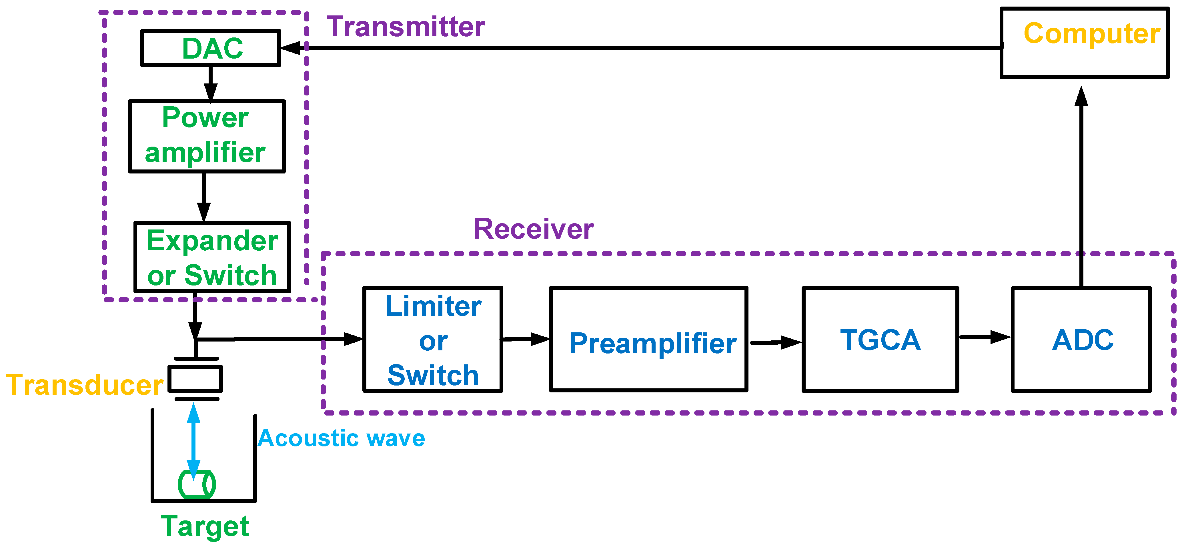
In diagnostic ultrasound imaging applications, the ultrasound systems are categorized into transmitters, receivers, and transducers [8,9,10]. Figure 1 shows the transducer, transmitter, and receiver in the ultrasound system used to describe the locations of the components of the preamplifier and time-gain compensation amplifier [11,12]. The computer-controlled digital-to-analog converter (DAC) produces low-voltage single or multiple-cycle pulse signals [13,14]. High-voltage pulse signals, amplified by the power amplifier in the transmitter, trigger the transducer through an expander or switch [15]. A limiter or switch protects the receiver from high-voltage or high-power signals generated by the power amplifiers because of the shared path between the transmitter and receiver [16].
The preamplifier is one of the first-stage receiver electronic devices after the transducer that amplifies weak acoustic signals with fewer noise effects [17]. Considering a transducer with low sensitivity requires a high input dynamic range of the preamplifier, the preamplifier used for ultrasound applications is a Class-A-type amplifier that continuously conducts voltage and current [18]. This preamplifier operates continuously during pulse transmission and echo reception; therefore, switches are utilized to block unwanted pulse signals and reduce power consumption; switches in the IC are normally implemented using voltage-controlled metal-oxide-semiconductor field-effect transistor (MOSFET) switches to save occupied chip space [19,20]. The low-voltage, current, or power signals received from the transducer are amplified by the preamplifier and time-gain-compensation amplifier (TGCA) in the receiver and then digitized with an analog-to-digital converter (ADC) to obtain the images [21]. The TGCA needs to amplify the weak signals further when the attenuation of the ultrasound signals is exponentially degraded, depending on the target distance [22]. In Figure 1, the transmitting and receiving beamforming components of the ultrasound transducer array are excluded to simplify the description of the entire ultrasound system. In a diagnostic photoacoustic system, the transmitter side is replaced by light-generating sources such as lasers, light-emitting diodes, or radio frequency sources [23,24,25].
The output of the capacitive micromachined ultrasonic transducer (CMUT) device is current; thus, a transimpedance amplifier is used to convert the current generated from the CMUT in the input to voltage in the preamplifier output [26]. Therefore, the preamplifiers were designed as voltage and current (transimpedance) amplifiers for the piezoelectric transducer and CMUT, respectively. The output of the piezoelectric transducer is a voltage; therefore, a low-noise voltage operational amplifier was used [27]. The preamplifier, also known as a low-noise amplifier (LNA), is used in piezoelectric transducers [26].
Section 2 describes the design parameters of the preamplifiers, such as voltage or current gain, bandwidth, direct current (DC) power consumption, and input- or output-referred noises, or noise figures. Section 3 presents the topology, design parameters, and circuit design techniques of previously reported preamplifiers for specific diagnostic ultrasound imaging applications such as CMUT, piezoelectric transducer, and imaging. Section 4 discusses the design topologies and criteria for the currently developed preamplifiers used for diagnostic ultrasound imaging applications and summarizes this review.
2. Design Parameters of the Preamplifiers for Ultrasound Transducer Types
The design parameters of preamplifiers for ultrasound transducer types are described in this section. Figure 2 shows the relationship between the design parameters of the preamplifiers used for diagnostic ultrasound imaging applications because design engineers for ultrasound components or systems need to consider the trade-off relationship at the design level. The design parameters of the preamplifiers were based on information from several textbooks on analog circuits, ICs, amplifiers, and ultrasound systems [28,29,30,31,32,33]. These design parameters are useful for circuit design engineers because some ultrasound systems require specific performance parameters.
The gain of the preamplifier is an important parameter because the weak echo signal generated by the transducer must be amplified. The voltage or current gain parameters are the extent to which the input signals are amplified [34]. Owing to the limited space for intravascular ultrasound (IVUS) applications, most research has focused on developing capacitive micromachined ultrasonic transducer devices with integrated circuits (IC) closely attached between the CMUT and IC [35]. For IVUS areas, the small size ultrasound transducers are required due to limited areas so the received echo signals are very weak so the high gain of the preamplifier is preferable. The bandwidth of the preamplifier is typically at least twice or higher than that of the transducer because the harmonic imaging mode requires the use of second or higher-order harmonic components to improve the image resolution [36]. The bandwidth can be increased while the gain reduces if the preamplifier has an operational amplifier topology [37]. A preamplifier design with a high gain has high power consumption because a high gain requires a high biasing current in the preamplifier [38,39]. While a preamplifier with high linearity is desirable for producing extremely weak acoustic signals from transducers, these signals affect the maximum gain performance of the amplifier.
The input third-order intercept point (IIP3) or the output third-order intercept point (OIP3) is the intercept point at which the component at the fundamental frequency and third-order intermodulation distortion points meet [40]. They are useful parameters to show the linearity of the preamplifiers. The higher the IIP3 or OIP3, the more linear the preamplifier works. Therefore, the circuit designers can increase the voltage gain before the intermodulation distortion is started [40]. In the harmonic imaging mode in the diagnostic ultrasound machine, high linearity is preferable because the unwanted harmonics need to be filtered out [26].
The direct current (DC) power consumption parameter was used because the preamplifier is a power-intensive electronic component when considering ultrasound receiver construction in the wireless ultrasound machine [41,42]. In addition, considering the preamplifier needs to enhance the weak signals, it needs to obtain high gain while sacrificing DC power consumption and occupied area [43,44]. For smartphone-based ultrasound systems with array transducers, area and power consumption are critical issues owing to the limited space and structures because unnecessary heat generation causes performance degradation during stable operation [45].
The input- and output-referred noises are the noise voltage and currents that generate the same output noises as the practical preamplifier generates if the ideal noise source is an input signal of the noise-free preamplifier [28]. The output-referred noise voltage of the preamplifier can be obtained by multiplying the gain and input-referred noise voltage of the preamplifier. The parameters of the input- and output-referred noise currents indicate the noise components of the preamplifier [46,47,48]—useful for demonstrating the noise contribution when amplifying weak echo signals through the preamplifier. Instead of input- or output-referred noise currents, a noise figure was used [49]. The preamplifier design is important because the gain of the first-stage amplifier contributes to the noise current in the receiver of the ultrasound system [50]. The noise figure (NF) equation is widely used in preamplifier design because it describes the noise contribution of the preamplifier [51]. As shown in (1), A1 needs to be as high as possible to reduce NF at the preamplifier [52].
where NF1 and NFn are the noise figures of the first- and n-stage preamplifiers, respectively; A1 and An−1 are the gains of the first- and n − 1-stage preamplifiers, respectively.
The following section presents a detailed schematic of the preamplifiers used in previously published articles on ultrasound applications.
3. Design Analysis of the Preamplifiers for Ultrasound Transducers
This section describes the design and schematic analysis of the design parameters of preamplifiers for specific ultrasound transducers, such as CMUT, piezoelectric transducer, and imaging. The labels and symbols in the articles are sometimes different from those in the selected articles; therefore, all schematic diagrams of the preamplifiers in this review paper were re-labeled and re-sketched, with some of the preamplifier designs also simplified to understand the operating mechanism more clearly for academic ultrasound researchers or design engineers. In the following sections, the same labels are used for input and output. B, N, and P indicate the Bipolar, N-channel metal-oxide semiconductor (NMOS), and P-channel metal-oxide-semiconductor (PMOS) transistors, respectively, while R, C, and I represent the resistor and capacitor, respectively.
3.1. Preamplifiers for CMUT Applications
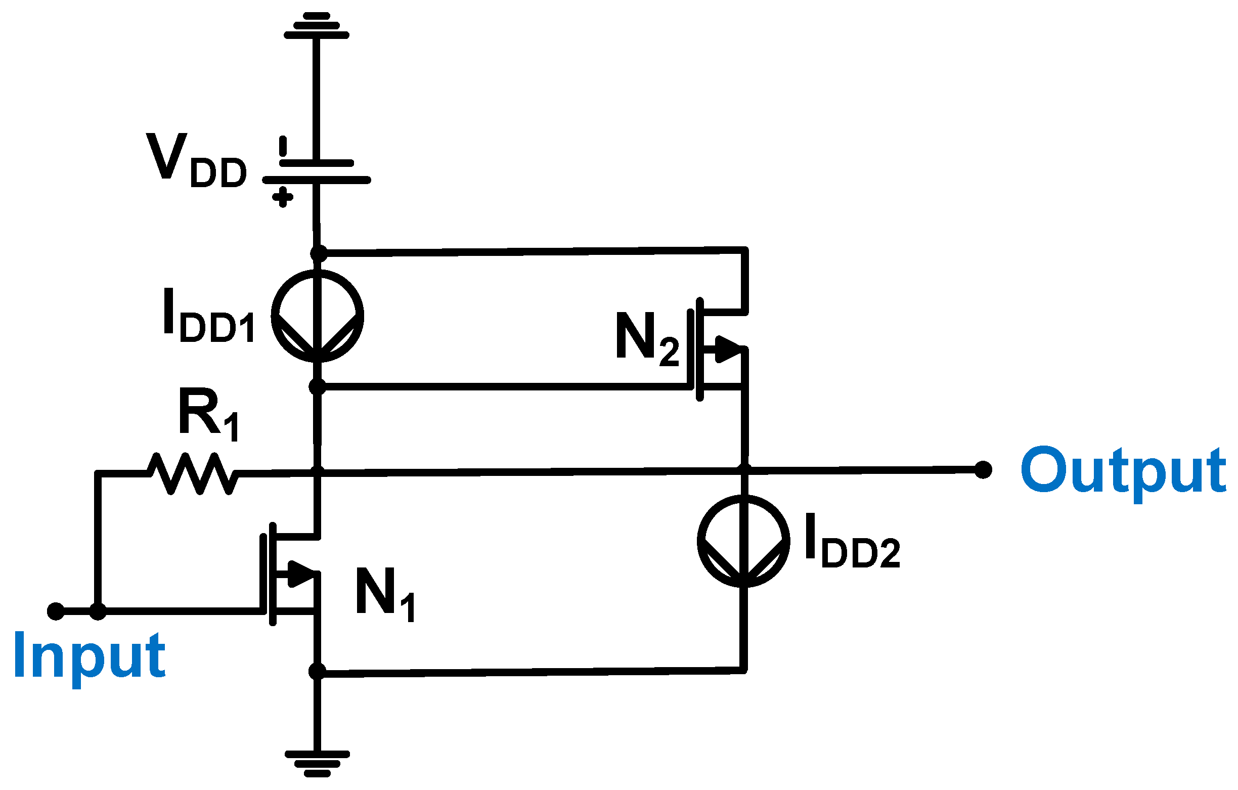
Figure 3 shows a schematic of the CMUT device preamplifier. The preamplifier was constructed using a common-source amplifier (N1 and IDD1), followed by a source follower (N2 and IDD2) with a feedback resistor (R1). The measured gain and bandwidth of the preamplifier were 215 kΩ and 25 MHz, respectively [53].
Figure 4 shows a schematic of the operational amplifier with resistor feedback loops (R2 and R3) of the CMUT device. The 0.8-μm CMOS process was used; thus, the DC supply voltage is 5 V (VDD) [54]. This operational amplifier comprises two stages. In the first stage, a differential cascade amplifier (B1, B2, N1, N2, and P1) is used. In the second stage, a source follower (P2 or N3) was used to reduce the output impedance of the amplifier. A resistor (R1) and a capacitor (C1) were used to reduce the phase shift of the frequency response [55]. The measured bandwidth, DC power consumption, and input noise voltage were 11 MHz, 2 mW, and 6.45 nV/√Hz, respectively [54].
Figure 5 shows the schematic of the common-source amplifier followed by the source follower with resistor feedback for CMUT array transducer applications. The 1.5-μm CMOS process was used; thus, the DC power supply is 5 V [56]. MOSFET switches are used to turn off the power [57]. The amplifier comprises a common-source amplifier (N1 and P3), followed by a source follower (N2 and N4). A source follower was used to reduce the impedance, thus increasing the amplifier bandwidth [57], which can be expressed by Equation (2).
where C1 is the feedback loop capacitance combined with the input parasitic capacitance.
The amplifier gain depends on the feedback resistance. The input-referred noise is inversely proportional to the feedback resistance (R1); therefore, a large R1 value is preferable [56]. However, the bandwidth is reduced. The bandwidth can be increased by decreasing the feedback resistance (R1) and feedback loop capacitance combined with the input parasitic capacitance (C1) [56]. However, the input-referred noise current is proportional to the √4kT/R1; thus, a relatively large feedback resistor is desirable if the input-referred noise current is an important design parameter [58]. The measured gain, input-referred noise current, bandwidth, and DC power consumption were 4.3 kΩ, 1.2 to 2.1 mPa/√Hz, 10 MHz, and 4 mW, respectively [56].
Figure 6 shows a schematic of the common-source amplifier (N1), followed by a source follower (N2 and N3) with a transistor feedback loop (N4 and N5) for the CMUT device. The 0.18-μm CMOS process was used [59]. The source-connected NMOS transistors (N4 and N5) were used for the transistor feedback loop to function as resistances controlled by the DC voltage (Vc). This topology is useful for reducing the chip area because physical resistors require large chip space [60,61,62]. The measured transimpedance gain, bandwidth, and input-referred noise are 951 dBΩ, 12 MHz, and 3.5 pA/√Hz, respectively [59].
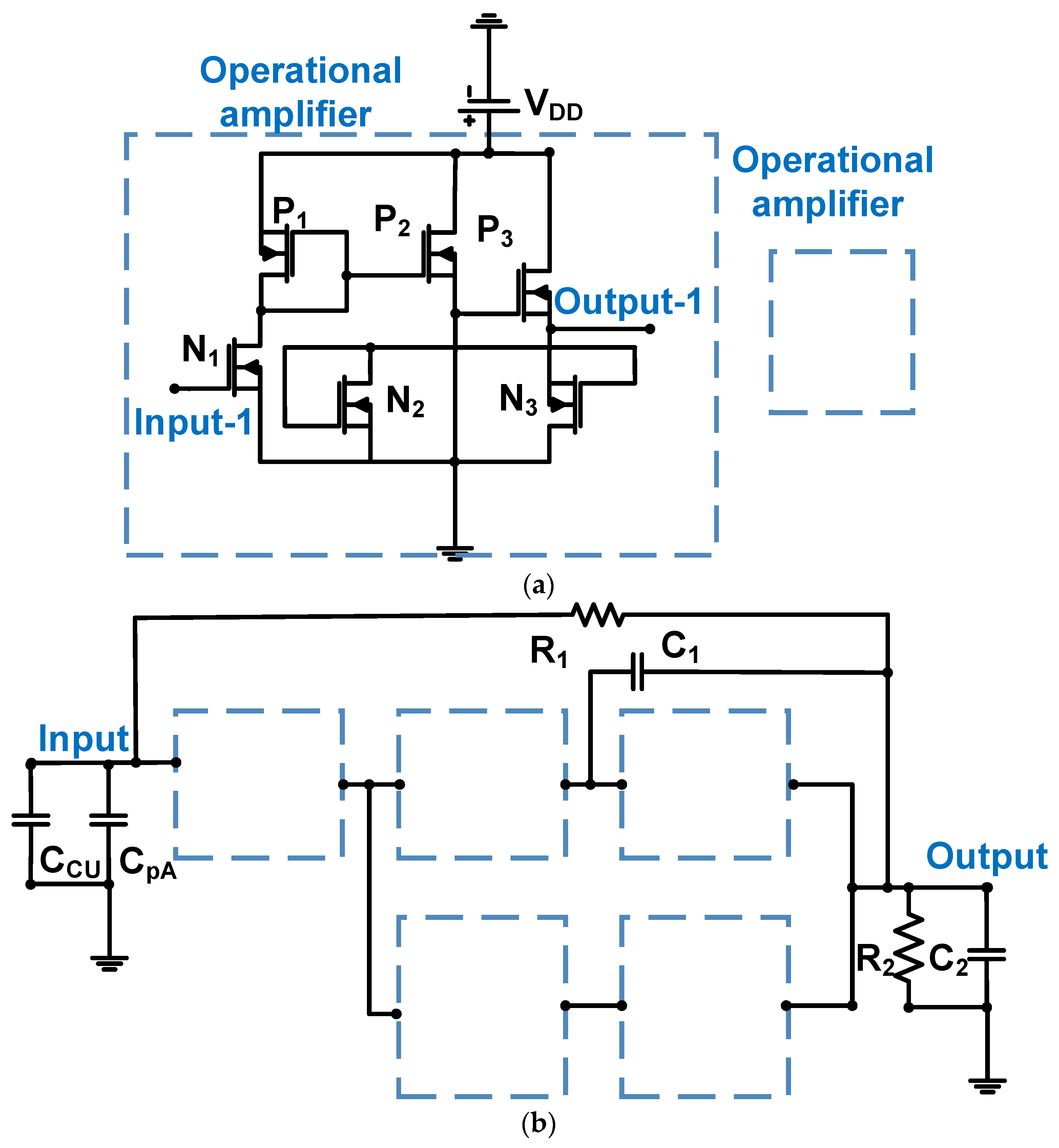
Figure 7a,b show the schematics of the operational amplifier with a resistor feedback loop for CMUT device applications. The 0.18-μm CMOS process was used [63]. The preamplifier was constructed using five operational amplifiers with a feedback resistor (R1) and a Miller capacitor (C1), as shown in Figure 7b. The Miller capacitor compensates for the pole and zero in the frequency response [64,65]. A current mirror (P1, P2, and P3) was used to reduce the power supply noise [66]. The output nodes (R2 and C2) are the input resistance and capacitance of the next stage of the electronics (ADC), respectively [63].
The input-referred current noise of the operational amplifier with resistor and capacitor feedback loop can be expressed in Equation (3) [63].
where RCU is the equivalent resistance of the CMUT and Cinput is the combined equivalent capacitance of the CMUT and the input parasitic capacitance at the input port.
The input-referred current noise is inversely proportional to the feedback resistance (R1) and input capacitance (Cinput). The measured bandwidth, DC power consumption, and input-referred noise current were 4.5 MHz, 370 μW, and 1.5524 pA/√Hz, respectively [63].
Figure 8 shows a schematic of the operational amplifier with a feedback loop (R1 and C1). The 0.18-μm CMOS process was used [67].
Several MOSFET switches were used to reduce DC power consumption if needed. Therefore, the active DC power consumption is 14.3 mW, whereas the inactive DC power consumption is 1.5 mW [67]. The transimpedance gain of the preamplifier (AZ) is expressed by Equation (4) [67].
where Zinput and Zfeedback are the input and feedback loop impedances, respectively; f and A are the operating frequency and open-loop gain of the operational amplifier, respectively.
The width of the NMOS (N1 and N2 = 2.3 mm) was sufficiently large to obtain a high current in the biasing circuit [67]. Different pairs and cascade stages were used to boost the gain and reduce the power supply noise, respectively, to achieve the high transimpedance gain (96.6 dBΩ) [67]. The Miller compensation capacitance (C2 = 5.4 pF) was used to increase the bandwidth; thus, the measured −3 dB bandwidth was 5.2 MHz [67]. The source follower (N6 = 135 μm/0.18 μm and N7 = 50 μm/0.63 μm) was used to reduce the output impedance, thus reducing the signal reflection to the next-stage component [67].
If the open loop gain of the amplifier (A) is large, the gain of the operational amplifier with feedback loop is dependent on the values of the resistance (R1 = 76 kΩ) and capacitance (C1 = 0.45 pF). The NF of the operational amplifier with feedback can be expressed by Equation (5) [67].
where Rinput and R1 are the input and feedback loop resistances, respectively; , , and are the input, output, and input voltage currents, respectively.
In Equation (5), a large feedback loop resistance (R1) is desirable to reduce the NF value. The measured NF of the operational amplifier with a feedback loop was 10.3 dB at 3 MHz [67].
Figure 9 shows a schematic of the operational amplifier with a voltage-controlled resistance (N5) for CMUT device applications.
Voltage-controlled resistance was implemented using the NMOS transistor to save space [69,70]. The resistance can be expressed using Equation (6) [68].
where μN is the carrier mobility, Cox is the unit-area gate capacitance, W and L are the channel width and length of the transistor, respectively, VC is the bias voltage, VOUPUT is the output voltage, and VTH is the threshold voltage of the transistor.
The input-referred current noise of the amplifier can be expressed by Equation (7) [68].
where Cin and CPR are the input and parasitic interconnect capacitances of the amplifier, respectively; CCU and RCU are the CMUT equivalent circuit capacitance and resistance, respectively; gm is the transconductance; T is room temperature; and id and iCU are the spectral densities of the current noise squares of the operational amplifier transistors and CMUT, respectively.
The input-referred current noise of the preamplifier is proportional to the input and parasitic interconnect capacitances of the preamplifier and the CMUT equivalent circuit capacitance but is inversely proportional to the voltage-controlled resistance [68].
The transimpedance gain of the preamplifier (AZ) is expressed in Equation (8) [68].
where ω0 and Q are the radian bandwidth and quality factor of the amplifier.
As shown in Equations (7) and (8), a high resistance (RN5) can lower the input-referred current noise and increase the transimpedance gain of the preamplifier. The measured DC power consumption, transimpedance gain, bandwidth, and input current noise density were 6.6 mW, 3 MΩ, 20 MHz, and 90 fA/√Hz, respectively [68].
Figure 10 shows a schematic of the two-stage operational amplifier with a capacitive feedback loop (C2 and C3) for the CMUT applications. The 0.35-μm CMOS process was used; thus, the DC power supply (VDD) is 3.3 V [71]. In the first stage, an operational amplifier was constructed using NMOS (N1) and PMOS (P1) transistors. In the second stage, the source follower was constructed using NMOS (N2) and PMOS (P3) transistors.
The operational amplifier comprises a capacitor feedback loop (C2 and C3). Therefore, the transfer function of the amplifier with a capacitor feedback loop (IZ) is expressed as Equation (9) [71].
where s is the complex operating frequency, ω0 is the radian bandwidth of the operational amplifier, gN2 is the transconductance of the MOSFET of N2, A is the open-loop voltage gain, and C1 is the combined capacitances of the CMUT and parasitic interconnection.
The gain of the operational amplifier with a capacitor feedback loop can be expressed by Equation (10) [71].
The measured −3 dB bandwidth, transimpedance gain, and DC power consumption were 40 MHz, 200 kΩ, and 0.8 mW, respectively. The input-referred spectral density of the amplifier current noise is expressed as Equation (11) [71].
where k is a process-dependent constant, gm is the MOSFET transconductance, id is the spectral density of the current noise square of the operational amplifier transistors, and idb is the spectral density of the current noise square of the current-bias circuit.
The transconductance (gN2) and load resistance (R1) must be high to reduce the input-referred spectral density of the amplifier current noise. The measured input referred noise at 20 MHz was 0.31 pA/√Hz [71].
3.2. Preamplifiers for Piezoelectric Transducer Applications
Figure 11 shows a schematic of the operational amplifier, followed by a source follower with a capacitor feedback loop for piezoelectric micromachined ultrasonic transducer (PMUT) array applications. The source follower is constructed using NMOS (N3) and PMOS (P3). The 0.13-μm CMOS process was used [72]. In the first stage, an operational amplifier was constructed using NMOS (N1) and PMOS (P1) transistors. In the second stage, a source follower was constructed using NMOS (N3) and PMOS (P3) transistors.
The output of the operational amplifier with a capacitive feedback loop (C1) can be simplified using Equation (12) if the open-loop gain of the amplifier is high [72].
where QE is the electric charge produced by the PMUT device and C1 is the feedback loop capacitance.
The input-referred current noise of the amplifier is proportional to the input capacitance of the operational amplifier (Cin) and feedback capacitance (C1); thus, it can be expressed using Equation (13) [72].
where Cin is the electric charge produced by the PMUT device, gN1, and gP1 are the transconductances of MOSFET N1 and P1, respectively, and inn and inp are the square root mean square current noises of MOSFET N1 and P1, respectively.
The voltage gain, bandwidth, DC power consumption, and input referred noise of the preamplifier were 21.8 dB, 22 MHz, 0.3 mW, and 7.1 nV/√Hz at 3 MHz, respectively [72].
Figure 12 shows a schematic of the low-noise amplifier (LNA) used for high-frequency piezoelectric transducer applications. The 0.18-μm BiCMOS process was used [73]. The LNA was constructed using a cascade amplifier (N1 and N3), followed by a common-source amplifier (N4) with a resonant load (R3, C2, L2, L3, and R4) owing to its high-frequency piezoelectric transducer characteristics [73].
The voltage gain of the amplifier can be expressed as Equation (14) [73]:
where gN1, gN3, and gN4 are the transconductances of MOSFET N1, N3, and N4, respectively, and CESD and CgsN1 are the ESD and gate-source parasitic capacitances of the MOSFET N1.
The voltage gain of the amplifier can be related to the load impedances (R3, R4, L2, L3, and C2), transconductance (gN1, gN3, and gN4), ESD parasitic capacitance, and gate-source parasitic capacitance of MOSFET N1. The measured voltage gain, bandwidth, and DC power consumption of LNA were 24.08, 73, and 43.57 mW, respectively [73].
The noise figure (NF) of the preamplifier can be expressed using Equation (15) [73].
where rN1 gate resistance of the MOSFET N1.
The NF of the LNA can be improved by a large transconductance (gN1) and low input, ESD parasitic capacitance, and gate-source parasitic capacitance of MOSFET N1 (C1, CESD, and CGSN1). The measured NF of the amplifier is 3.51 dB [73].
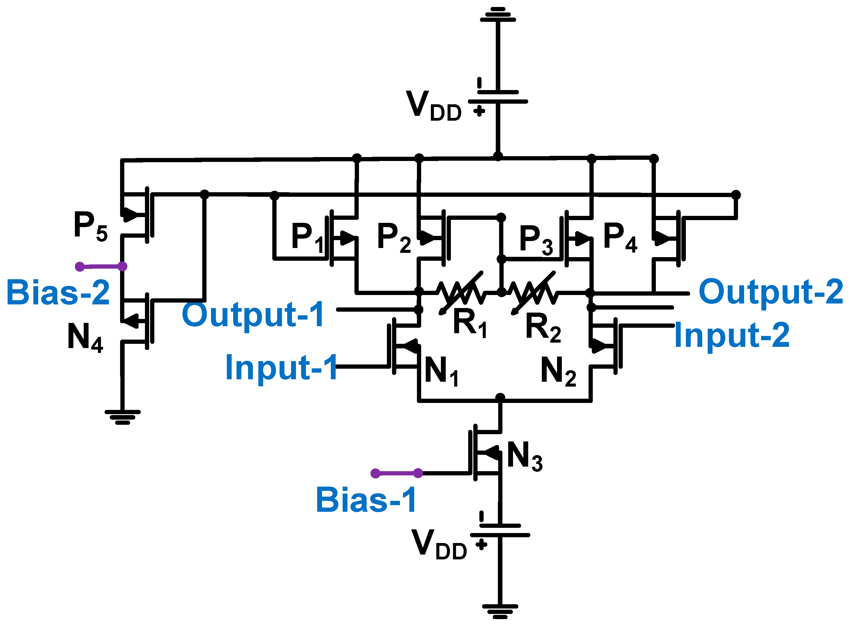
Figure 13 shows a schematic of the preamplifier used in piezoelectric transducer applications. The acoustic signals from the ultrasound transducer were sent to the Input-1 port, with the common ground of the transducer connected to the Input-2 port [74]. The voltage gain depends on the variable resistors (R1 and R2) and the transistor sizes (N1, P2, N2, and P3). The measured gain, bandwidth, and NF of the preamplifier were 20, 75, and 10 dB, respectively [74].
Figure 14 shows a schematic of an LNA. The 0.18-μm CMOS process was used; thus, the DC supply voltage (VDD) is 3 V [75].
The LNA is constructed using a three-stage common-source amplifier. The transistors (N1 and P2) were biased to obtain the 600 μA current (IDD1) and 800 μA current (IDD2), respectively [75]. Resistor (R1) can prevent leakage currents for long-cycle pulse signals and capacitor C1 can be programmed with 6-dB steps [75]. Therefore, the gain of the LNA (AI) can be expressed by Equation (16) [75].
The measured center frequency, bandwidth, and input-referred noise current were 13 MHz, 21 MHz, and 4 nA/√Hz [75].
Figure 15 shows a schematic of the variable LNA with a resistor feedback loop for the piezoelectric transducer because the LNA topology is preferable for low impedance [76]. A variable LNA with a resistor feedback loop was used because of the signal attenuation of echo signals in deep areas [77]. The 0.18-μm CMOS process was used [77]. This two-stage variable LNA structure had a feedback loop composed of two variable resistors (R1 and R4). The first stage of the LNA is a cascade amplifier composed of an NMOS (N1 and N2) and PMOS (P1, P2, and P3), and the second stage is the source follower (N4 and P5). A variable Miller capacitor (C1) is used to increase the bandwidth by improving the phase margins [78]. A MOSFET switch composed of transistors (N5 and P6) was used to reduce the power consumption of the LNA during the period when the driving pulse signals were applied.
The voltage gain of the LNA can be expressed as Equation (17) [77]:
The measured gain, bandwidth, and input-referred noise voltage of the variable LNA with resistor feedback loop were 32 dB, 11 MHz, and 4.1 nV/√Hz, respectively [77].
3.3. Preamplifier for Ultrasound Imaging Applications
Figure 16 shows a schematic of the LNA for ultrasound imaging applications. The 0.18-μm CMOS process was used [79]. The LNA was constructed using a three-stage operational amplifier with feedback resistors (R7 and R8) and variable input resistors (R1 and R2 = 0.2, 0.4, 0.8, and 1.6 kΩ) [79]. The PMOS inputs were used to reduce the noise of the preamplifier. The gain of the LNA was dependent on the variable resistors (R1, R2, R7, and R8). The measured gain, bandwidth, OIP3, and input-referred noise current of the LNA were 15.6 dB, 10 MHz, 2.64 Vp-p, and 6.3 nV/√Hz, respectively [79].
4. Discussion and Conclusions
This review will guide the design characteristics of preamplifiers for ultrasound transducer applications. For ultrasound applications, currently used most IC fabrication processes are 0.13 μm, 0.18 μm, or 0.8 μm because the supply voltage of the 0.13 μm, 0.18 μm, and 0.8 μm IC fabrication processes are 1.8 V, 3.3 V, and 5 V, respectively. Below the 0.13-μm process, the supply voltage is lower than 1.8 V; as a result, the maximum achievable gain of the preamplifier could be limited even though high dynamic ranges of the preamplifier are desirable. Therefore, a new IC fabrication process may not be desirable even if the sizes of the new IC fabrication processes are smaller.
The primary design parameters of the preamplifier are gain, bandwidth, noise figure (or input- or output-referred noise), power consumption, and IIP3 or OIP3 [80,81]. These design parameters of the preamplifiers have a trade-off relationship; therefore, circuit or system designers must consider the parameter specifications for the performance of ultrasound transducers. For example, the bandwidth of a preamplifier should be larger than that of an ultrasound transducer. The input-referred noise of the preamplifier must be similar to or lower than that of the ultrasound transducer. The gain of the preamplifier should be high if the sensitivity of the transducer used in the IVUS applications is low. However, the bandwidth of the preamplifier for the operational amplifier type can be increased if its gain of the preamplifier needs is decreased [82]. While a high biasing current can increase the gain of the preamplifier, it causes unnecessary DC power consumption; therefore, an appropriate current is desirable at the design level [83]. A preamplifier with a wide bandwidth can increase the number of unwanted harmonic components of the acoustic signals generated by the ultrasound transducer. While a high linearity of the preamplifier can be obtained if a current-biasing circuit based on the MOSFET is used, it causes high DC power consumption [84].
For CMUT device applications, a transimpedance amplifier—an operational amplifier with a feedback loop composed of resistors or capacitors—is preferred for high impedances [85,86]. For piezoelectric devices, the LNA is preferable because of the low impedance of the piezoelectric transducer [72].
To increase the gain of the preamplifier, circuit designers use a common-source amplifier with a large width of the first transistor connected to the input port or use a cascade topology to obtain a high current from the biasing circuit [28]. However, this causes relatively high DC power consumption. In the last stage, the source follower is used to reduce the output impedance, thus smoothly passing the amplified signal to the next-stage amplifier or ADC. In an operational amplifier with a resistor feedback loop, the feedback resistor affects the gain and bandwidth of the preamplifier.
For the input-referred noise or NF, the transconductance value of the MOSFET is important because it can affect the noise of the preamplifier [87]. For an operational amplifier with a feedback resistor loop, the feedback resistor can affect the noise parameters [66]. In addition, the open-loop gain of the operational amplifier must be large to reduce the input-referred noise [28]. MOSFET switches can be used to reduce power consumption during the driving pulse period when transmitted signals are applied [88]. Instead of resistors, voltage-controlled MOSFETs for amplifier design could help reduce the chip area [88]. However, this scheme may require an integrated preamplifier design with a more complex and accurate timing period after pulse transmission. In particular, this technique can help reduce power consumption in wireless ultrasound systems. Miller capacitors in the output port are sometimes used to increase the bandwidth by moving the pole and zero locations [30]. An operational amplifier with a capacitive feedback loop was used for the PUMT device, which has a lower impedance than that of the CMUT [72]. An LNA with a resonant load was developed for high-frequency piezoelectric transducers [73]. The LNA constructed using a three-stage common-source amplifier used resistors to prevent leakage currents for a long-cycle transmission period and a capacitor to provide a 6-dB step gain [77].
Table 1 summarizes the design parameters of the previously published preamplifiers used for ultrasound transducers. As shown in Table 1, the gain of the transimpedance amplifier is expressed by dBΩ or kΩ units because the input is current and the output is voltage. The input-referred noise (IRN) can be expressed by current or voltage units, and the NF can be expressed on the dB scale. Topologies can be classified into common source, operational amplifier, or low-noise amplifier types.
While several review papers on IC components for ultrasound systems have been published, they did not provide specific design guidelines for preamplifiers used in ultrasound transducer applications. Therefore, this is the first review paper of preamplifiers to provide design guidelines for ultrasound transducer applications, such as capacitive micromachined ultrasonic transducer (CMUT), piezoelectric transducer, and ultrasound imaging applications.
In ultrasound imaging, preamplifiers are required to amplify weak acoustic signals and obtain images for diagnostic purposes. However, their performance is limited because of transistor requirements. Therefore, the design parameters of the gain, bandwidth, input- or output-referred noise currents, and DC power consumption are described to explain the design concepts of the preamplifiers because they have a trade-off relationship when designing the preamplifier components used for diagnostic ultrasound imaging applications
Recently, with the emergence of new ultrasound applications such as photoacoustic imaging, smartphone touch sensors, wireless ultrasound machines, brain stimulation, and ultrasound-combined positron emission tomography, academic researchers have used commercial components or system IC for these emerging applications. However, further performance optimization is possible if ultrasound transducers with appropriate electronic selection or a design topology that considers a trade-off relationship are developed. As such, the knowledge of preamplifier design in this review paper is expected to be helpful in this regard.
Funding
This work was supported by the National Research Foundation of Korea (NRF) grant funded by the Korea government (MSIT) (No. 2020R1A2C4001606).
Institutional Review Board Statement
Not applicable.
Informed Consent Statement
Not applicable.
Data Availability Statement
Data are contained within the article.
Conflicts of Interest
The author declares no conflicts of interest.
Abbreviations
| AC | Alternating current |
| DC | Direct current |
| ADC | Analog-to-digital converter |
| DAC | Digital-to-analog converter |
| CMUT | Capacitive micromachined ultrasonic transducer |
| DAC | Digital-to-analog converter |
| IIP3 | Third-order input intercept point |
| OIP3 | Third-order output intercept point |
| NMOS | N-channel MOS |
| PMOS | P-channel MOS |
| MOSFET | Metal-oxide-semiconductor field-effect transistor |
| THD | Total harmonic distortion |
| PMUT | Piezoelectric micromachined ultrasonic transducer |
| TIA | Transimpedance amplifier |
| LNA | Low-noise amplifier |
| VGA | Variable gain amplifier |
| PGA | Programmable gain amplifier |
| TGCA | Time gain compensation amplifier |
| CMOS | Complementary Metal-oxide-semiconductor |
| IVUS | Intravascular ultrasound system |
| SNR | Signal-to-noise ratio |
| NF | Noise figure |
| IC | Integrated circuit |
| IRN | Input-referred noise current |
| ASIC | Asynchronous semiconductor integrated circuit |
| ESD | Electrostatic discharge device |
References
- Zhang, T.; Liang, H.; Wang, Z.; Qiu, C.; Peng, Y.; Zhu, X.; Li, J.; Ge, X.; Xu, J.; Huang, X.; et al. Piezoelectric ultrasound energy–harvesting device for deep brain stimulation and analgesia applications. Sci. Adv. 2022, 8, eabk0159. [Google Scholar] [CrossRef]
- Jung, U.; Ryu, J.; Choi, H. Optical Light Sources and Wavelengths within the Visible and Near-Infrared Range Using Photoacoustic Effects for Biomedical Applications. Biosensors 2022, 12, 1154. [Google Scholar] [CrossRef]
- Jung, U.; Choi, H. Active echo signals and image optimization techniques via software filter correction of ultrasound system. Appl. Acoust. 2022, 188, 108519. [Google Scholar] [CrossRef]
- Zhong, S.; Cai, Q.; Zhong, L.; Wang, Y.; Liang, F.; Deng, Z.; Li, S.; Zha, D.; Qiu, W.; Wu, J. Low-Intensity Focused Ultrasound Ameliorates Ischemic Heart Failure Related to the Cholinergic Anti-Inflammatory Pathway. J. Ultrasound Med. 2023, 42, 463–475. [Google Scholar] [CrossRef]
- Lee, J.E.; Jeon, H.-J.; Lee, O.J.; Lim, H.G. Diagnosis of diabetes mellitus using high frequency ultrasound and convolutional neural network. Ultrasonics 2024, 136, 107167. [Google Scholar] [CrossRef]
- Zhang, J.; Long, X.; Zhang, G.; Ma, Z.; Li, W.; Wang, Y.; Yang, F.; Lin, R.; Li, C.; Lam, K.-H. Broadband transparent ultrasound transducer with polymethyl methacrylate as matching layer for in vivo photoacoustic microscopy. Photoacoustics 2023, 33, 100548. [Google Scholar] [CrossRef]
- Lin, R.; Zhang, Q.; Lv, S.; Zhang, J.; Wang, X.; Shi, D.; Gong, X.; Lam, K.-h. Miniature intravascular photoacoustic endoscopy with coaxial excitation and detection. J. Biophotonics 2023, 16, e202200269. [Google Scholar] [CrossRef]
- He, Z.; Chen, G.; Wang, Y.; Zhang, K.; Tian, W. Finite Element Calculation with Experimental Verification for a Free-Flooded Transducer Based on Fluid Cavity Structure. Sensors 2018, 18, 3128. [Google Scholar] [CrossRef]
- Lim, H.G.; Kim, H.; Kim, K.; Park, J.; Kim, Y.; Yoo, J.; Heo, D.; Baik, J.; Park, S.-M.; Kim, H.H. Thermal Ablation and High-Resolution Imaging Using a Back-to-Back (BTB) Dual-Mode Ultrasonic Transducer: In Vivo Results. Sensors 2021, 21, 1580. [Google Scholar] [CrossRef]
- Li, J.; Ma, Y.; Zhang, T.; Shung, K.; Zhu, B. Recent Advancements in Ultrasound Transducer: From Material Strategies to Biomedical Applications. BME Front. 2022, 2022, 9764501. [Google Scholar] [CrossRef] [PubMed]
- Kripfgans, O.D.; Chan, H.-L. Ultrasonic Imaging: Physics and Mechanism; Springer International Publishing: Berlin, Germany, 2021. [Google Scholar] [CrossRef]
- Yoon, C.; Kang, J.; Song, T.k.; Chang, J.H. Elevational Synthetic Aperture Focusing for Three-Dimensional Photoacoustic Imaging Using a Clinical One-Dimensional Array Transducer. IEEE Trans. Biomed. Eng. 2022, 69, 2817–2825. [Google Scholar] [CrossRef]
- Lurton, X. An Introduction to Underwater Acoustics: Principles and Applications; Springer: London, UK, 2002. [Google Scholar]
- Weibao, Q.; Yanyan, Y.; Fu Keung, T.; Lei, S. A multifunctional, reconfigurable pulse generator for high-frequency ultrasound imaging. IEEE Trans. Ultrason. Ferroelectr. Freq. Control 2012, 59, 1558–1567. [Google Scholar] [CrossRef]
- Choi, H. A Doherty Power Amplifier for Ultrasound Instrumentation. Sensors 2023, 23, 2406. [Google Scholar] [CrossRef] [PubMed]
- Shung, K.K. Diagnostic Ultrasound: Imaging and Blood Flow Measurements; Taylor & Francis: Boca Raton, FL, USA, 2015. [Google Scholar]
- Zhang, Z.; Liu, R.; Li, G.; Su, M.; Li, F.; Zheng, H.; Qiu, W. A Dual-Mode 2D Matrix Array for Ultrasound Image-Guided Noninvasive Therapy. IEEE Trans. Biomed. Eng. 2021, 68, 3482–3490. [Google Scholar] [CrossRef] [PubMed]
- Choi, H. Development of negative-group-delay circuit for high-frequency ultrasonic transducer applications. Sens. Actuators A 2019, 299, 111616. [Google Scholar] [CrossRef]
- Baker, R.J. CMOS: Mixed-Signal Circuit Design; John Wiley & Sons: Hoboken, NJ, USA, 2008. [Google Scholar]
- Johns, D.A.; Martin, K. Analog Integrated Circuit Design; John Wiley & Sons: New York, NY, USA, 2008. [Google Scholar]
- Suri, J.S.; Kathuria, C.; Chang, R.-F.; Molinar, F.; Fenster, A. Advances in Diagnostic and Therapeutic Ultrasound Imaging; Artech House: Norwood, MA, USA, 2008. [Google Scholar]
- Jun-ru, W.; Wesley, N. Emerging Therapeutic Ultrasound; World Scientific Publishing: Hackensack, NJ, USA, 2006. [Google Scholar]
- Li, J.; Xu, J.; Liu, X.; Zhang, T.; Lei, S.; Jiang, L.; Ou-Yang, J.; Yang, X.; Zhu, B. A novel CNTs array-PDMS composite with anisotropic thermal conductivity for optoacoustic transducer applications. Compos. Part B 2020, 196, 108073. [Google Scholar] [CrossRef]
- Jung, U.; Choi, J.H.; Choo, H.T.; Kim, G.U.; Ryu, J.; Choi, H. Fully Customized Photoacoustic System Using Doubly Q-Switched Nd: YAG Laser and Multiple Axes Stages for Laboratory Applications. Sensors 2022, 22, 2621. [Google Scholar] [CrossRef] [PubMed]
- Choi, H.; Ryu, J.-M.; Choe, S.-w. A novel therapeutic instrument using an ultrasound-light-emitting diode with an adjustable telephoto lens for suppression of tumor cell proliferation. Measurement 2019, 147, 106865. [Google Scholar] [CrossRef]
- Szabo, T.L. Diagnostic Ultrasound Imaging: Inside Out; Elsevier Academic Press: London, UK, 2013. [Google Scholar]
- Kim, K.; Choi, H. High-efficiency high-voltage class F amplifier for high-frequency wireless ultrasound systems. PLoS ONE 2021, 16, e0249034. [Google Scholar] [CrossRef]
- Razavi, B. Design of Analog CMOS Integrated Circuits; McGraw-Hill Science: New York, NY, USA, 2016. [Google Scholar]
- Sevic, J.F. The Load-Pull Method of RF and Microwave Power Amplifier Design; John Wiley & Sons: Hoboken, NJ, USA, 2020. [Google Scholar]
- Talbot, D.B. Practical Analog and RF Electronics; CRC press: Boca Raton, FL, USA, 2020. [Google Scholar]
- Osgood, R., Jr.; Meng, X. Principles of Photonic Integrated Circuits; Springer: Berlin, Germany, 2021. [Google Scholar]
- Halak, B. Ageing of Integrated Circuits: Causes, Effects and Mitigation Techniques; Springer: Berlin, Germany, 2019. [Google Scholar]
- Shutilov, V.A.; Alferieff, M.E. Fundamental Physics of Ultrasound; CRC Press: Boca Raton, FL, USA, 2020. [Google Scholar]
- Bugg, D.V. Electronics: Circuits, Amplifiers and Gates; CRC Press: Boca Raton, FL, USA, 2021. [Google Scholar]
- Zhou, Q.; Lau, S.; Wu, D.; Shung, K.K. Piezoelectric films for high frequency ultrasonic transducers in biomedical applications. Prog. Mater. Sci. 2011, 56, 139–174. [Google Scholar] [CrossRef]
- Arnau, A. Piezoelectric Transducers and Applications; Springer: Berlin, Germany, 2004. [Google Scholar]
- Yawale, S.; Yawale, S. Operational Amplifier; Springer: Berlin, Germany, 2022. [Google Scholar]
- Chen, W.-K. Analog Circuits and Devices; CRC Press: Boca Raton, FL, USA, 2003. [Google Scholar]
- Carr, J. RF Components and Circuits; Elsevier: Amsterdam, The Netherlands, 2002. [Google Scholar]
- Eroglu, A. Linear and Switch-Mode RF Power Amplifiers: Design and Implementation Methods; CRC Press: Boca Raton, FL, USA, 2017. [Google Scholar]
- Mason, T.J.; Peters, D. Practical Sonochemistry: Power Ultrasound Uses and Applications; Woodhead Publishing: Cambridge, UK, 2002. [Google Scholar]
- Iniewski, K. Medical Imaging; Wiley Online Library: Hoboken, NJ, USA, 2009. [Google Scholar]
- Benesty, J.; Huang, G.; Chen, J.; Pan, N. Microphone Arrays; Springer: Berlin, Germany, 2023. [Google Scholar]
- Self, D. Small Signal Audio Design; Focal Press: Waltham, MA, USA, 2020. [Google Scholar]
- McCafferty, J.; Forsyth, J.M. Point of Care Ultrasound Made Easy; CRC Press: Boca Raton, FL, USA, 2020. [Google Scholar]
- Gonzalez, G. Microwave Transistor Amplifiers: Analysis and Design; Prentice hall: New Jersey, NJ, USA, 1997. [Google Scholar]
- Allen, P.E.; Holberg, D.R. CMOS Analog Circuit Design; Oxford University Press: Oxford, UK, 2002. [Google Scholar]
- Donnay, S.; Gielen, G. Substrate Noise Coupling in Mixed-Signal ASICs; Springer: Berlin, Germnay, 2003. [Google Scholar]
- Albulet, M. RF Power Amplifiers; SciTech Publishing: London, UK, 2001. [Google Scholar]
- Leblebici, D.; Leblebici, Y. Fundamentals of High-Frequency CMOS Analog Integrated Circuits; Cambridge University Press New York: Cambridge, UK, 2009. [Google Scholar]
- Razavi, B. RF Microelectronics; Prentice Hall: Upper Saddel River, NJ, USA, 2011. [Google Scholar]
- Chang, K. Microwave Solid-State Circuits and Applications; Wiley: New York, NY, USA, 1994. [Google Scholar]
- Wygant, I.O.; Jamal, N.S.; Lee, H.J.; Nikoozadeh, A.; Oralkan, O.; Karaman, M.; Khuri-Yakub, B.T. An integrated circuit with transmit beamforming flip-chip bonded to a 2-D CMUT array for 3-D ultrasound imaging. IEEE Trans. Ultrason. Ferroelectr. Freq. Control 2009, 56, 2145–2156. [Google Scholar] [CrossRef]
- Ciçek, I.; Bozkurt, A.; Karaman, M. Design of a front-end integrated circuit for 3D acoustic imaging using 2D CMUT arrays. IEEE Trans. Ultrason. Ferroelectr. Freq. Control 2005, 52, 2235–2241. [Google Scholar] [CrossRef]
- Gray, P.R. Analysis and Design of Analog Integrated Circuits; John Wiley & Sons: Hoboken, NJ, USA, 2009. [Google Scholar]
- Wygant, I.O.; Xuefeng, Z.; Yeh, D.T.; Oralkan, O.; Ergun, A.S.; Karaman, M.; Khuri-Yakub, B.T. Integration of 2D CMUT arrays with front-end electronics for volumetric ultrasound imaging. IEEE Trans. Ultrason. Ferroelectr. Freq. Control 2008, 55, 327–342. [Google Scholar] [CrossRef] [PubMed]
- Ding, Y.; Harjani, R. High-Linearity CMOS RF Front-End Circuits; Springer Science & Business Media: Berlin, Germany, 2004. [Google Scholar]
- Gift, S.J.; Maundy, B. Electronic Circuit Design and Application; Springer: Berlin, Germany, 2020. [Google Scholar]
- Banuaji, A.; Cha, H.-K. A 15-V bidirectional ultrasound interface analog front-end IC for medical imaging using standard CMOS technology. IEEE Trans. Circuits Syst. II Express Briefs 2014, 61, 604–608. [Google Scholar] [CrossRef]
- Wang, A.Z. On-Chip ESD Protection for Integrated Circuits: An IC Design Perspective; Springer Science & Business Media: Berlin, Germany, 2006. [Google Scholar]
- Voinigescu, S. High-Frequency Integrated Circuits; Cambridge University Press: Cambridge, UK, 2013. [Google Scholar]
- Wang, A. Practical ESD Protection Design; John Wiley & Sons: Hoboken, NJ, USA, 2021. [Google Scholar]
- Cheng, T.-C.; Tsai, T.-H. CMOS ultrasonic receiver with on-chip analog-to-digital front end for high-resolution ultrasound imaging systems. IEEE Sens. J. 2016, 16, 7454–7463. [Google Scholar] [CrossRef]
- Darabi, H. Radio Frequency Integrated Circuits and Systems; Cambridge University Press: Cambridge, UK, 2015. [Google Scholar]
- Bera, S.C. Microwave High Power High Efficiency GaN Amplifiers for Communication; Springer Nature: Berlin, Germany, 2022. [Google Scholar]
- Hartnagel, H.L.; Quay, R.; Rohde, U.L.; Rudolph, M. Fundamentals of RF and Microwave Techniques and Technologies; Springer: Berlin, Germany, 2023. [Google Scholar]
- Chen, K.; Lee, H.-S.; Chandrakasan, A.P.; Sodini, C.G. Ultrasonic imaging transceiver design for CMUT: A three-level 30-Vpp pulse-shaping pulser with improved efficiency and a noise-optimized receiver. IEEE J. Solid-State Circuits 2013, 48, 2734–2745. [Google Scholar] [CrossRef]
- Gurun, G.; Hasler, P.; Degertekin, F.L. Front-end receiver electronics for high-frequency monolithic CMUT-on-CMOS imaging arrays. IEEE Trans. Ultrason. Ferroelectr. Freq. Control 2011, 58, 1658–1668. [Google Scholar] [CrossRef] [PubMed]
- LaMeres, B.J. Introduction to Logic Circuits & Logic Design with VHDL; Springer: Berlin, Germany, 2023. [Google Scholar]
- Roy, S. Advanced Digital System Design: A Practical Guide to Verilog Based FPGA and ASIC Implementation; Springer: Berlin, Germany, 2023. [Google Scholar]
- Gurun, G.; Tekes, C.; Zahorian, J.; Xu, T.; Satir, S.; Karaman, M.; Hasler, J.; Degertekin, F.L. Single-chip CMUT-on-CMOS front-end system for real-time volumetric IVUS and ICE imaging. IEEE Trans. Ultrason. Ferroelectr. Freq. Control 2014, 61, 239–250. [Google Scholar] [CrossRef] [PubMed]
- Zamora, I.; Ledesma, E.; Uranga, A.; Barniol, N. Miniaturized 0.13-μm CMOS front-end analog for AlN PMUT arrays. Sensors 2020, 20, 1205. [Google Scholar] [CrossRef] [PubMed]
- Choi, H.; Li, X.; Lau, S.-T.; Hu, C.; Zhou, Q.; Shung, K.K. Development of Integrated Preamplifier for High-Frequency Ultrasonic Transducers and Low-Power Handheld Receiver. IEEE Trans. Ultrason. Ferroelectr. Freq. Control 2011, 58, 2646–2658. [Google Scholar] [CrossRef]
- Kim, I.; Kim, H.; Griggio, F.; Tutwiler, R.L.; Jackson, T.N.; Trolier-McKinstry, S.; Choi, K. CMOS ultrasound transceiver chip for high-resolution ultrasonic imaging systems. IEEE Trans. Biomed. Circuits Syst. 2009, 3, 293–303. [Google Scholar] [CrossRef] [PubMed]
- van Willigen, D.M.; Kang, E.; Janjic, J.; Noothout, E.; Chang, Z.-Y.; Verweij, M.D.; De Jong, N.; Pertijs, M.A. A transceiver ASIC for a single-cable 64-element intra-vascular ultrasound probe. IEEE J. Solid-State Circuits 2021, 56, 3157–3166. [Google Scholar] [CrossRef]
- Rohde, U.L.; Rudolph, M. RF/Microwave Circuit Design for Wireless Applications; John Wiley & Sons: Hoboken, NJ, USA, 2013. [Google Scholar]
- Jung, G.; Tekes, C.; Rashid, M.W.; Carpenter, T.M.; Cowell, D.; Freear, S.; Degertekin, F.L.; Ghovanloo, M. A reduced-wire ICE catheter ASIC with Tx beamforming and Rx time-division multiplexing. IEEE Trans. Biomed. Circuits Syst. 2018, 12, 1246–1255. [Google Scholar] [CrossRef] [PubMed]
- Steer, M. Microwave and RF Design; NC State University: Raleigh, NC, USA, 2019. [Google Scholar]
- Kim, T.; Shin, S.; Kim, S. An 80.2 dB DR 23.25 mW/channel 8-channel ultrasound receiver with a beamforming embedded SAR ADC. IEEE Trans. Circuits Syst. II Express Briefs 2018, 66, 1487–1491. [Google Scholar] [CrossRef]
- Kumar, N.; Grebennikov, A. Distributed Power Amplifiers for RF and Microwave Communications; Artech House: Norwood, MA, USA, 2015. [Google Scholar]
- Baker, R.J. CMOS: Circuit Design, Layout, and Simulation; John Wiley & Sons: Hoboken, NJ, USA, 2019. [Google Scholar]
- Larson, L.E. RF and Microwave Circuit Design for Wireless Communications; Artech House: Norwood, MA, USA, 1996. [Google Scholar]
- Kenington, P.B. High Linearity RF Amplifier Design; Artech House, Inc.: Norwood, MA, USA, 2000. [Google Scholar]
- Free, C.E.; Aitchison, C.S. RF and Microwave Circuit Design: Theory and Applications; John Wiley & Sons: Hoboken, NJ, USA, 2021. [Google Scholar]
- Uchino, K. Advanced Piezoelectric Materials: Science and Technology; Woodhead Publishing: Cambridge, UK, 2017. [Google Scholar]
- Kang, H.; Sun, Y.; Wodnicki, R.; He, Q.; Zeng, Y.; Lu, G.; Yeom, J.Y.; Yang, Y.; Zhou, Q. 2-D Array Design and Fabrication With Pitch-Shifting Interposer at Frequencies From 4 MHz up to 10 MHz. IEEE Trans. Ultrason. Ferroelectr. Freq. Control 2022, 69, 3382–3391. [Google Scholar] [CrossRef]
- Vendelin, G.D.; Pavio, A.M.; Rohde, U.L.; Rudolph, M. Microwave Circuit Design Using Linear and Nonlinear Techniques; John Wiley & Sons: Hoboken, NJ, USA, 2021. [Google Scholar]
- Grebennikov, A.; Sokal, N.O.; Franco, M.J. Switchmode RF Power Amplifiers; Newnes: Amsterdam, The Netherlands, 2011. [Google Scholar]
Figure 1.
Block diagram of the transducer and ultrasound transmitter and receiver used for diagnostic ultrasound imaging applications.
Figure 1.
Block diagram of the transducer and ultrasound transmitter and receiver used for diagnostic ultrasound imaging applications.

Figure 2.
Design parameters of the preamplifiers used for ultrasound transducers.

Figure 3.
Preamplifier for CMUT device. Adapted with permission from Ref. [53]. Copyright 2009, IEEE.
Figure 3.
Preamplifier for CMUT device. Adapted with permission from Ref. [53]. Copyright 2009, IEEE.

Figure 4.
Operational amplifier with a resistor feedback loop for the CMUT device. Adapted with permission from Ref. [54]. Copyright 2005, IEEE.
Figure 4.
Operational amplifier with a resistor feedback loop for the CMUT device. Adapted with permission from Ref. [54]. Copyright 2005, IEEE.

Figure 5.
Common-source amplifier followed by a source follower with resistor feedback for the CMUT device. Adapted with permission from Ref. [56]. Copyright 2008, IEEE.
Figure 5.
Common-source amplifier followed by a source follower with resistor feedback for the CMUT device. Adapted with permission from Ref. [56]. Copyright 2008, IEEE.

Figure 6.
Common-source amplifier followed by a source follower with a transistor feedback loop for the CMUT device (biasing circuits are not shown for simplified analysis). Adapted with permission from Ref. [59]. Copyright 2014, IEEE.
Figure 6.
Common-source amplifier followed by a source follower with a transistor feedback loop for the CMUT device (biasing circuits are not shown for simplified analysis). Adapted with permission from Ref. [59]. Copyright 2014, IEEE.

Figure 7.
(a) Operational amplifier and (b) operational amplifier with a resistor feedback loop for CMUT. Adapted with permission from Ref. [63]. Copyright 2016, IEEE.
Figure 7.
(a) Operational amplifier and (b) operational amplifier with a resistor feedback loop for CMUT. Adapted with permission from Ref. [63]. Copyright 2016, IEEE.

Figure 8.
Feedback-resistor-based operational amplifier for CMUT device. Adapted with permission from Ref. [67]. Copyright 2013, IEEE.
Figure 8.
Feedback-resistor-based operational amplifier for CMUT device. Adapted with permission from Ref. [67]. Copyright 2013, IEEE.

Figure 9.
Operational amplifier with resistor feedback for CMUT device. Adapted with permission from Ref. [68]. Copyright 2011, IEEE.
Figure 9.
Operational amplifier with resistor feedback for CMUT device. Adapted with permission from Ref. [68]. Copyright 2011, IEEE.

Figure 10.
Feedback-capacitor-based operational amplifier for CMUT devices used in the IVUS and ICE device applications. Adapted with permission from Ref. [71]. Copyright 2014, IEEE.
Figure 10.
Feedback-capacitor-based operational amplifier for CMUT devices used in the IVUS and ICE device applications. Adapted with permission from Ref. [71]. Copyright 2014, IEEE.

Figure 11.
Operational amplifier with a capacitor feedback loop for the PMUT device. Adapted from Zamora et al. [72] with permission under the terms of the CC BY 4.0 License, Copyright 2020 MDPI AG.
Figure 11.
Operational amplifier with a capacitor feedback loop for the PMUT device. Adapted from Zamora et al. [72] with permission under the terms of the CC BY 4.0 License, Copyright 2020 MDPI AG.

Figure 12.
LNA for piezoelectric transducer devices (electrostatic discharge device (ESD) and electrostatic capacitors not shown for simplified analysis). Adapted with permission with Ref. [73]. Copyright 2011, IEEE.
Figure 12.
LNA for piezoelectric transducer devices (electrostatic discharge device (ESD) and electrostatic capacitors not shown for simplified analysis). Adapted with permission with Ref. [73]. Copyright 2011, IEEE.

Figure 13.
Preamplifier for piezoelectric transducer device (biasing circuits not shown for simplified analysis) [74]. Copyright 2009, IEEE.
Figure 13.
Preamplifier for piezoelectric transducer device (biasing circuits not shown for simplified analysis) [74]. Copyright 2009, IEEE.

Figure 14.
LNA for piezoelectric transducer device (switch circuits not shown because they are not related to analysis). Adapted with permission from Ref. [75]. Copyright 2021, IEEE.
Figure 14.
LNA for piezoelectric transducer device (switch circuits not shown because they are not related to analysis). Adapted with permission from Ref. [75]. Copyright 2021, IEEE.

Figure 15.
Variable LNA for piezoelectric transducer device. Adapted with permission from Ref. [77]. Copyright 2018, IEEE.
Figure 15.
Variable LNA for piezoelectric transducer device. Adapted with permission from Ref. [77]. Copyright 2018, IEEE.

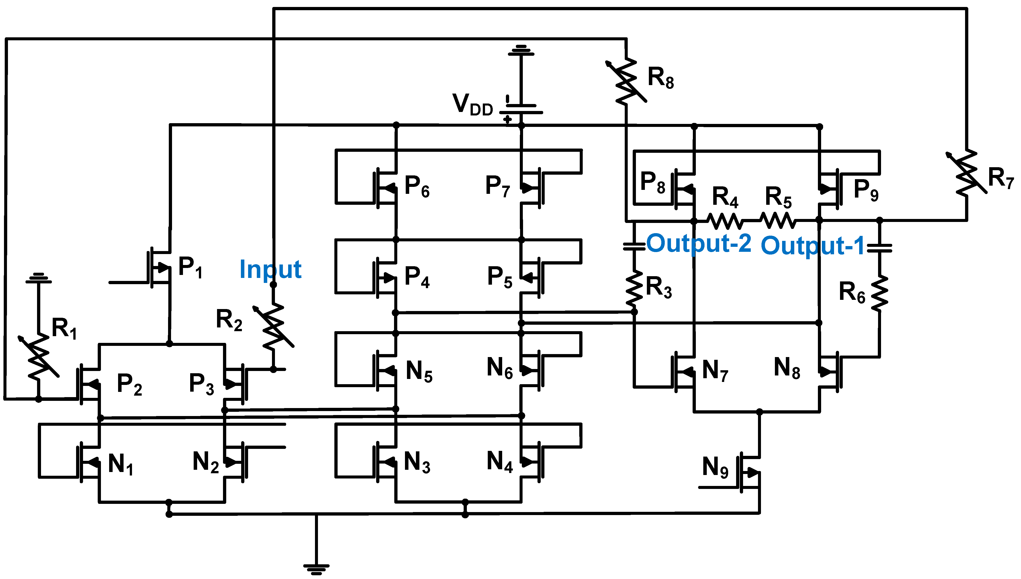
Figure 16.
LNA for 3-D ultrasound imaging applications. Adapted with permission Ref. [79]. Copyright 2018, IEEE.
Figure 16.
LNA for 3-D ultrasound imaging applications. Adapted with permission Ref. [79]. Copyright 2018, IEEE.


Table 1.
Summary of the preamplifiers currently used for ultrasound transducer research.
| Paper | Gain | Bandwidth | DC Power Consumption | IIP3 or OIP3‘ | IRN | NF | Topology | Application |
|---|---|---|---|---|---|---|---|---|
| [53] | 215 kΩ | 25 MHz | – | – | – | – | Common-source amplifier and source follower with a feedback resistor | CMUT |
| [54] | – | 11 MHz | 2 mW | – | 6.45 nV/√Hz | – | Operational amplifier with resistor feedback | CMUT |
| [56] | 4.3 kΩ | 10 MHz | 4 mW | – | 2.1 mPa/√Hz | – | Common-source amplifier and source follower with a feedback resistor | CMUT |
| [59] | 95.1 dBΩ | 12 MHz | – | – | 3.5 pA/√Hz | – | Common-source amplifier and source follower with a transistor feedback loop | CMUT |
| [63] | – | 4.5 MHz | 0.37 mW | – | 1.5524 pA/√Hz | – | Operational amplifier with resistor feedback | CMUT |
| [67] | 96.6 dBΩ | 5.2 MHz | 14.3 mW | 618 mV (OIP3) | – | 10.3 dB | Operational amplifier with a feedback loop | CMUT |
| [68] | 3 MΩ | 20 MHz | 6.6 mW | – | 90 fA/√Hz | – | Operational amplifier with resistor feedback | CMUT |
| [71] | 200 kΩ | 40 MHz | 0.8 mW | – | 0.31 pA/√Hz | – | Operational amplifier with capacitor feedback | CMUT |
| [72] | 21.8 dB | 22 MHz | 0.3 mW | – | 7.1 nV/√Hz | – | Operational amplifier with resistor feedback | Piezoelectric transducer |
| [73] | 24.08 dB | 73 MHz | 43.57 mW | −3.5 dBm (IIP3) | – | 3.51 dB | Low-noise amplifier with a resonant circuit | Piezoelectric transducer |
| [74] | 20 dB | 75 MHz | – | – | – | 10 dB | Operational amplifier with resistor feedback | Piezoelectric transducer |
| [75] | 69 dB | 21 MHz | – | – | 4 nA/√Hz | – | Low-noise amplifier | Piezoelectric transducer |
| [77] | 32 dB | 11 MHz | – | – | 4.1 nV/√Hz | – | Variable low-noise amplifier with resistor feedback | Piezoelectric transducer |
| [79] | 15.6 dB | 10 MHz | – | 2.64 Vp-p (OIP3) | 6.3 nV/√Hz | – | Low-noise amplifier | Imaging |
Disclaimer/Publisher’s Note: The statements, opinions and data contained in all publications are solely those of the individual author(s) and contributor(s) and not of MDPI and/or the editor(s). MDPI and/or the editor(s) disclaim responsibility for any injury to people or property resulting from any ideas, methods, instructions or products referred to in the content. |
© 2024 by the author. Licensee MDPI, Basel, Switzerland. This article is an open access article distributed under the terms and conditions of the Creative Commons Attribution (CC BY) license (https://creativecommons.org/licenses/by/4.0/).
Share and Cite
MDPI and ACS Style
Choi, H. Design of Preamplifier for Ultrasound Transducers. Sensors 2024, 24, 786. https://doi.org/10.3390/s24030786
AMA Style
Choi H. Design of Preamplifier for Ultrasound Transducers. Sensors. 2024; 24(3):786. https://doi.org/10.3390/s24030786
Chicago/Turabian StyleChoi, Hojong. 2024. "Design of Preamplifier for Ultrasound Transducers" Sensors 24, no. 3: 786. https://doi.org/10.3390/s24030786
Note that from the first issue of 2016, this journal uses article numbers instead of page numbers. See further details here.