
An Improved Active Damping Method for Enhancing Robustness of LCL-Type, Grid-Tied Inverters under Weak Grid Conditions
School of Automation, Northwestern Polytechnical University, Xi’an 710129, China
*
Author to whom correspondence should be addressed.
Sensors 2023, 23(19), 8203; https://doi.org/10.3390/s23198203
Submission received: 9 August 2023
/
Revised: 11 September 2023
/
Accepted: 28 September 2023
/
Published: 30 September 2023
(This article belongs to the Section Electronic Sensors)
Abstract
:The conventional proportional-gain-feedback link can only obtain the smallest effective damping region (EDR) due to the control delay among all the active damping methods regarding the capacitor current feedback. The digitally controlled system tends to be unstable when the system resonant frequency reaches the critical frequency caused by the grid impedance variation. To weaken the adverse effect on the system caused by the control delay, phase-lead feedback links are applied along the feedback path to provide phase compensation. By taking the simplicity and reliability of the feedback links into account, this paper proposes an alternative to an ideal differentiator, which consists of the Tustin discrete form of ‘s’ and a digital low-pass filter. This proposed method has an identical phase frequency characteristic as an ideal differentiator but a better magnitude frequency characteristic, and its EDR can reach [0, fs/3]. The system stability analysis is conducted under different resonant frequencies, and under the condition of a weak grid, the co-design approach of the active damper and digital controller is presented. Finally, the experimental results are shown to verify the proposed method.
1. Introduction
At present, the main way to develop renewable energy on a large scale is distributed generation based on renewable energy. As the energy conversion interface between the renewable energy power generation unit and the power grid, a grid-connected inverter is used to convert DC energy into high-quality AC and feed it into the power grid. Generally, a suitable filter needs to be added between the inverter and the power grid. Compared with the L filter, the LCL filter contains filter capacitance, so it has smaller volume and stronger high-frequency filtering ability [1,2,3,4]. However, LCL filters introduce a pair of conjugate poles on the closed-loop stability boundary, which is likely to impair system stability [5,6]. To address the issue, various active damping methods are usually used [7,8].
Active damping techniques are mainly divided into two kinds including the single-loop structure of the grid current feedback and the dual-loop structure of the grid current plus capacitor current feedback. The former means fewer sensors and software-based observers are needed, for which the single-loop current control schemes have increasingly been studied [9,10,11,12,13,14,15,16]. Reference [15] shows that a stable single-loop control scheme of the grid current without damping is implemented for the reason that an inherent damping characteristic is introduced when the digital delay is considered. The inherent damping characteristic is, however, available in the frequency region beyond one sixth of the system sampling frequency. The system will become unstable as a result of the wide variation of the resonance frequencies in the weak grid. Reference [16] proposed an active damping technique with a negative high-pass filter along the grid current feedback path, which helps to mitigate the phase lag caused by time delays found in the digital implement. A first-order, high-pass filter can only provide phase compensation less than π/2. In order to attain bigger phase compensation, hence bigger EDR, [17] introduced an improved active damping scheme by adding a delay link along the damping loop mentioned in [16], which is equivalent to cascading one more first-order, high-pass filter. A second-order, high-pass filter can provide sufficient phase compensation to counteract the negative influence caused by time delay, and hence, enlarge the EDR. Although only one quantity needs to be measured and fewer sensors are needed in single-loop techniques, the system performance can be affected due to variation of the parameters. The latter is commonly used in practice for its excellent damping effect and simple implementation [18,19,20,21,22,23]. The traditional capacitor current feedback active damping (CCFAD) adopts a proportional gain feedback of the capacitor current, which establishes an EDR in the frequency range [0, fs/6] due to the control delay. Here, fs/6 is defined as the critical frequency between the positive and negative damping region [24]. As a result, a lot of literature is devoted to increasing EDR through different strategies that improve the capacitor current feedback loop. A second-order-generalized-integrator-based time-delay compensation method for extending the stable region is presented in [25], which can compensate a maximum delay of a half-sampling period and the EDR can be increased up to fs/4. Reference [26] introduces a first-order leading link and [27] proposes a delayed feedback link into the capacitor current feedback loop, respectively. Though both methods achieve some phase compensation, they have a relatively small EDR, i.e., [0, fs/4]. Many efforts have been focused on achieving better frequency derivative characteristics whose corresponding critical frequency is fs/3, aiming to further increase the critical frequency. A virtual RC damping method is proposed in [28], where the extra virtual capacitance and inductance benefit the delay compensation and the EDR is enlarged up to [0, fs/3]. References [29,30] introduce the derivative term to counteract the time delay; however, the digital implement of the proposed method is not discussed. A first-order, high-pass filter is applied in [31] to mimic derivative features, which have a better disturbance rejection capability. The phase compensation amount can be modified by varying the high-pass filter parameters, hence changing the size of the critical frequency. However, a large phase lag error means a smaller EDR whose critical frequency is above fs/4, but away from fs/3. The nonideal generalized integrator (nGI) [32] has so far proven to be the best way to realize the highly accurate derivative. Reference [33] proposes two digital differentiators, as simple alternatives of nGI, which are first-order differentiators based on a backward Euler plus digital lead compensator and a second-order differentiator based on a Tustin plus digital notch filter. These methods can obtain better differential characteristics at higher frequencies; hence, the critical frequencies are closer to fs/3 in comparison with the high-pass filter. However, their critical frequencies cannot approach fs/3 due to the small phase lag in the mid- and high-frequency domains. Accordingly, the damping limitation and stability challenge will occur at the critical frequency fs/3 [34]. Reference [35] introduces a new feedback link of capacitor–current based on the recursive infinite impulse response digital filter, which is equivalent to a high-order, high-pass filter with sufficient phase lead compensation. The EDR is extended close to the maximum value fs/2. However, the high-order filter in the digital control is unreliable and imposes complexity on the control system. The phase compensation link used in [36] is a second-order, high-pass filter whose magnitude in the middle and low frequency domains is almost zero, and it can provide a greater phase lead. However, it ignores the frequency characteristic of the second-order filter in the high-frequency region, especially near the Nyquist frequency.
This article proposed an alternative of the ideal differentiator, which consists of the ideal differentiator’s Tustin discrete form and a digital low-pass filter. The proposed methods are consistent with the ideal differentiator in phase characteristics, which ensure the phase compensation can achieve π/2; namely, the corresponding EDR is [0, fs/3]. Also, the magnitude characteristics of the proposed method stay approximately constant in the middle- and low-frequency region and are attenuated greatly in the high-frequency region, which ensures the noise rejection capability.
This paper is organized as follows: Section 2 introduces the system model and conducts the impedance-based analysis in the continuous s-domain; Section 3 depicts the property of the proposed method in the discrete z-domain and deduces the discretization or digitally controlled system; Section 4 conducts the stability analysis of the system with the proposed active damping method; Section 5 introduces the co-design procedure of the digital controller and active damper; and Section 6 presents the experimental results and validates the theoretical analysis. Finally, the conclusion of this paper is shown in Section 7.
2. Continuous S-Domain Analysis
2.1. System Description
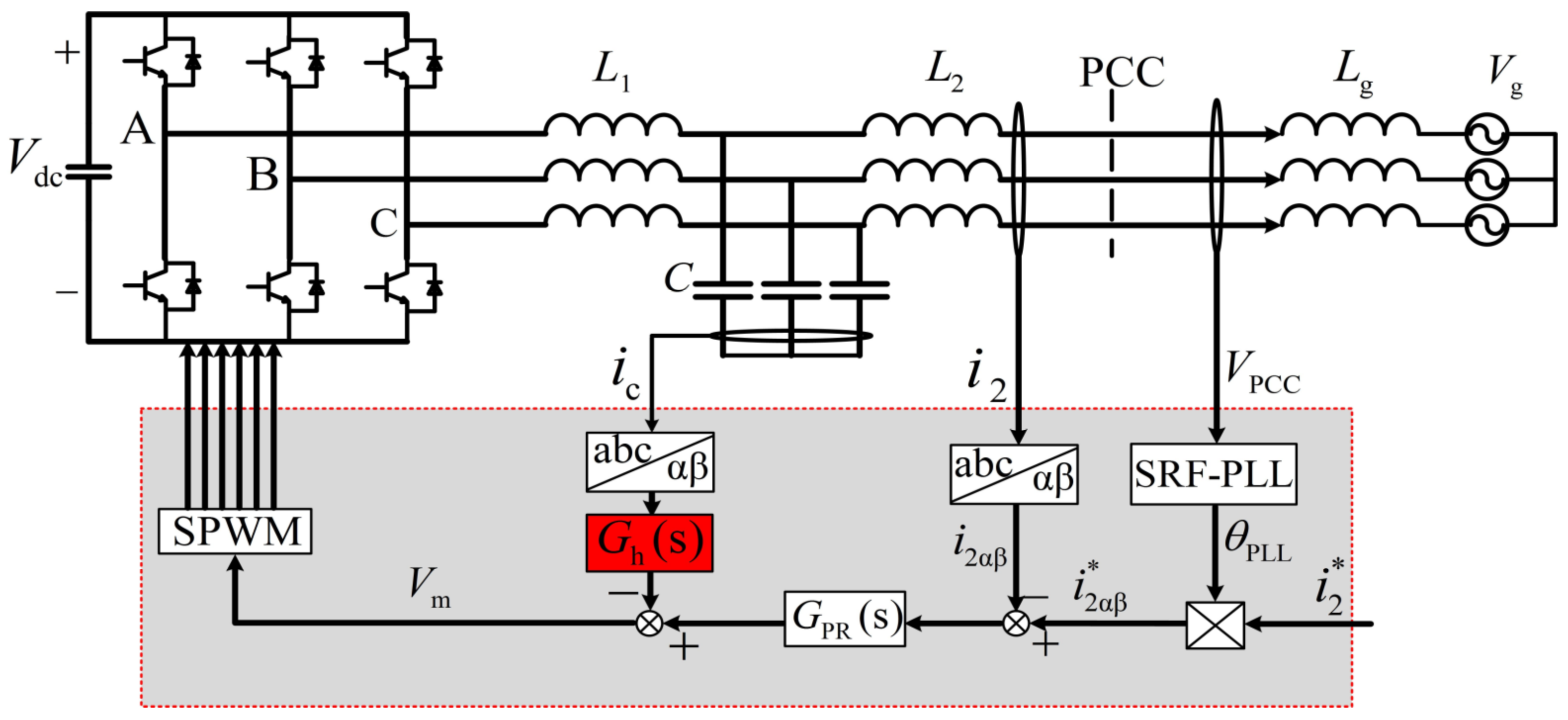
Figure 1 shows the general structure of a three-phase, grid-connected, voltage-source inverter (VSI) with an LCL filter and constant DC-link voltage Vdc. For the sake of analysis simplicity, the following two assumptions are considered valid, one of which is that the parasitic resistances of the circuit are neglected, which results in the worst damping condition, and the other of which is that the grid voltage is assumed to be balanced. In Figure 1, Lg represents the grid inductance which is variable, Gh(s) is the feedback block of capacitor current ic, and GPR(s) is the current regulator that generally applies a proportional plus resonance (PR) controller, which can provide substantial gain at fundamental frequency; the transfer function is given by (1) [37].
where KP and Kr are proportional and resonant coefficients, respectively, and ωi is the −3 dB bandwidth for which generally ωi =π rad/s [38]. For such current regulators, the steady-state tracking error is substantially eliminated at the fundamental frequency ωo.
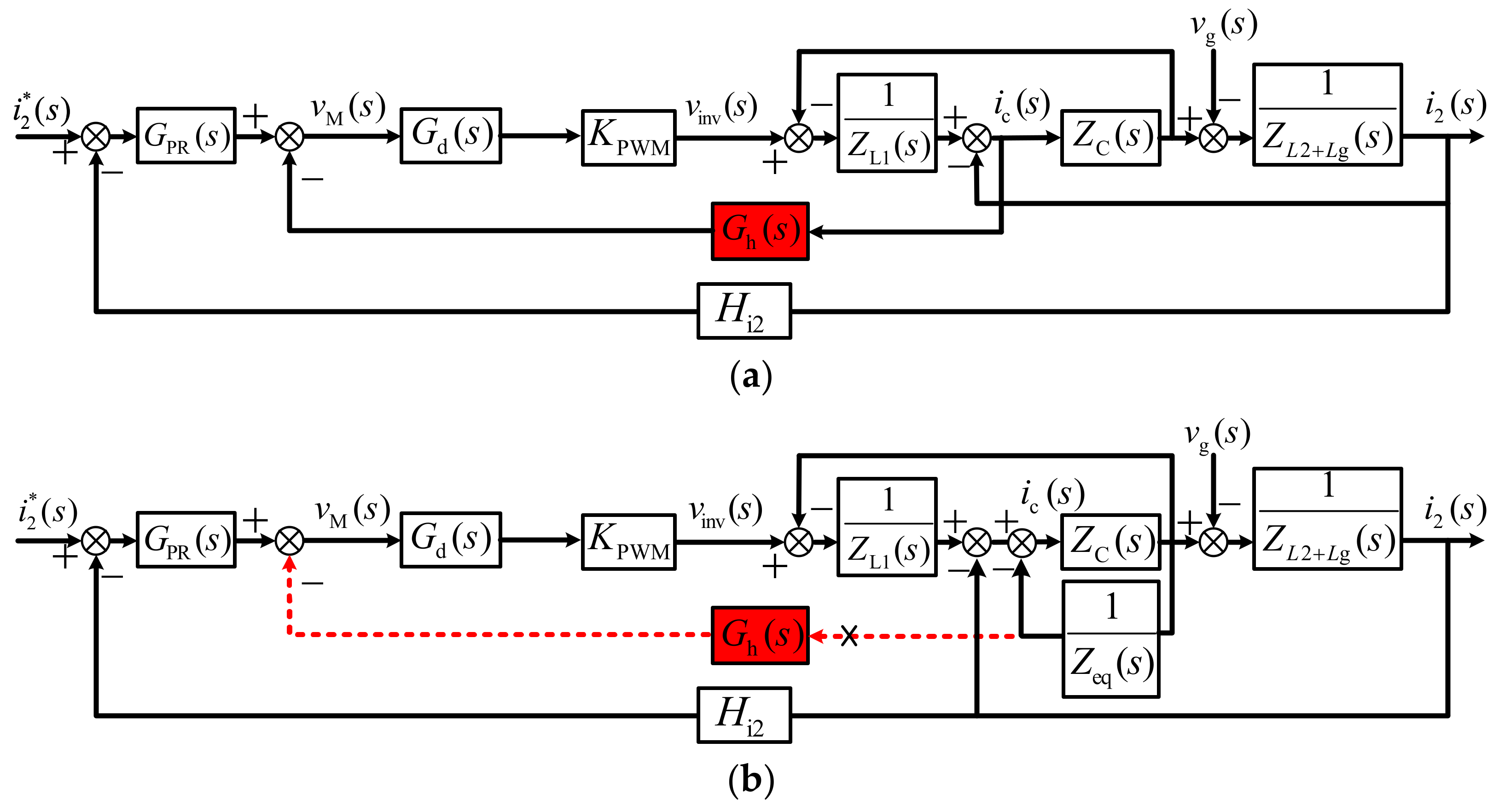
Figure 2 depicts the per-phase block diagrams of the LCL-type, grid-tied inverter system with CCFAD. i2 is the measured grid current; is the command grid current which is set according to the system request; ic is the measured capacitor current, and the inverter is modeled as a linear gain KPWM with one and half sampling period digital delay Gd(s) which is composed of a computation delay and a modulation delay. The expression of Gd(s) is given as follows [39]:
where Ts is the system sampling period.
2.2. Impedance-Based Analysis
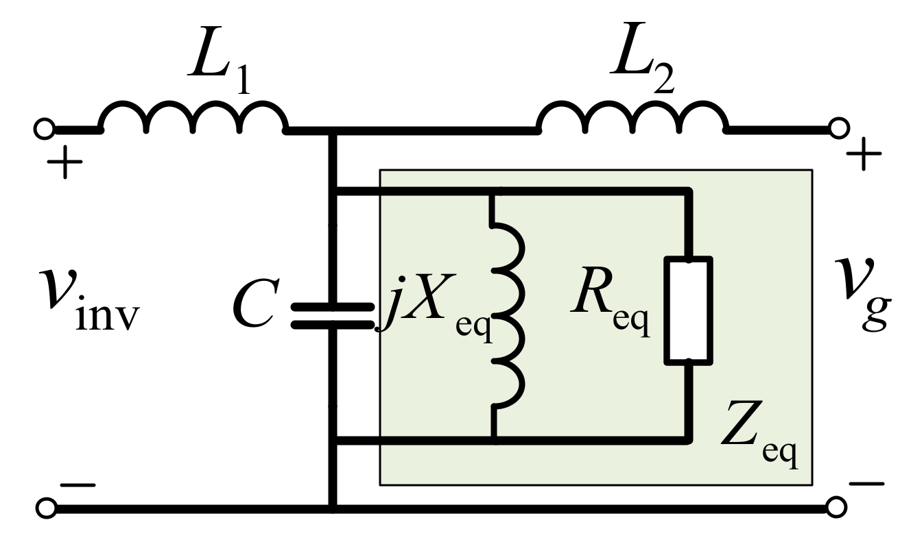
To better demonstrate the damping mechanism of the active damping method realized by the capacitor current feedback and keep the system closed-loop characteristics unchanged, some modifications are introduced on the model shown in Figure 2a and the equivalent block diagram is shown in Figure 2b. Obviously, it can be seen that the feedback coefficient of the capacitor current is equivalent to be an impedance Zeq paralleled with the capacitor. As shown in Figure 3, a virtual inductance Xeq and a virtual resistance Req are connected in parallel and constitute impedance Zeq, which is represented by (3)
where Gh(s) is the feedback coefficient, which has all-pass or high-pass filter (HPF) characteristics due to ic being the high-frequency current signal. For analysis simplicity, the first-order HPF are studied in this paper. The general expression of first-order HPF can be given as follows:
where Kd represents the gain of HPF, ωd represents the cutoff frequency of the HPF. Transformed into the polar coordinate form, Gh(s) consists of two parts presented in (4), where A is the modulus and θ is the lead-phase angle with the boundary values 0 and π/2 not included in the range available. Substituting (4) into (3) and doing some simple mathematical operation, (5) can be attained.
Substituting s = jω into (5), the expression of Req, Xeq can be attained in the frequency domain.
where RA = L1/(CKPWMA), which is the equivalent resistance of CCFAD in analog control.
As shown in (6), the real term Req(ω) and the imaginary term Xeq(ω) can both become negative after introducing the finite delay time and lead phase angle. The equivalent resonant frequency will make a difference compared with the actual resonant frequency ωr after introducing the imaginary term Xeq(ω).
Xeq(ω) acts like an inductance when Xeq(ω) is positive, which counteracts the effect of the capacitor; the resonant frequency thus becomes a little higher than ωr. On the contrary, Xeq(ω) acts like a capacitor when Xeq(ω) is negative, which enhances the effect of the capacitor; the resonant frequency thus becomes a little lower than ωr.
The negative real term causes the nonminimum-phase behavior, which adds open-loop right half-plane poles (RHP) to the current control loop and thus impairs the system robust stability. From (6), to be positive for Req(ω), the critical frequency fcrit can be attained as follows:
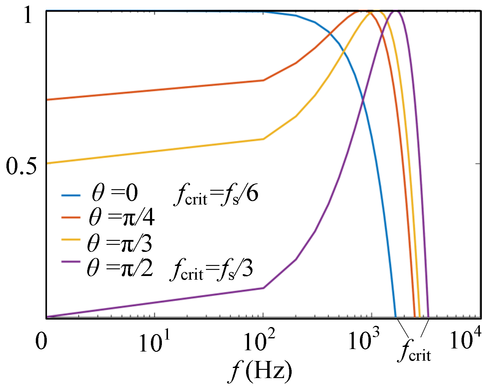
As shown in (8), when θ changes from 0 to π/2, fcrit increases from fs/6 to fs/3. Figure 4 plots the frequency region of Req(ω) being positive as θ changes. Especially, taking the two boundary values into account, it is seen that when θ = 0, fcrit = fs/6, and when θ = π/2, fcrit = fs/3. Therefore, the EDR obtained is [0, fs/3) according to (8).
3. Discrete Z-Domain Analysis
3.1. Improved Active Damping Method
In order to study the damping mechanism of the feedback link in a digitally controlled system, the discrete form of Gh(s) is needed. The Tustin discrete expression of the feedback link Gh(s) is shown in (9).
where H = 2 Kd/(2 + ωdTs), a = (ωdTs − 2)/(ωdTs + 2), (−1 < a < 1).
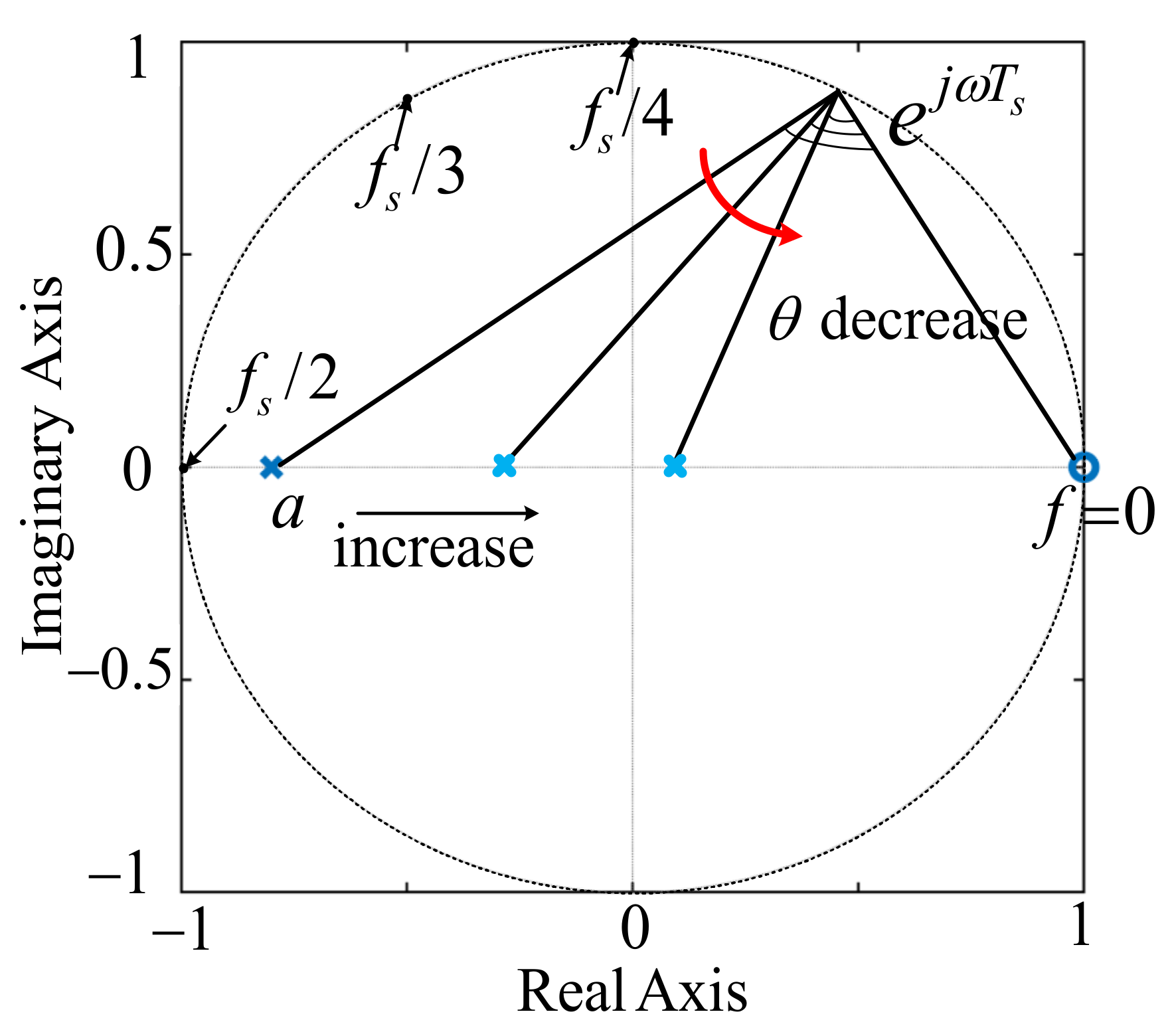
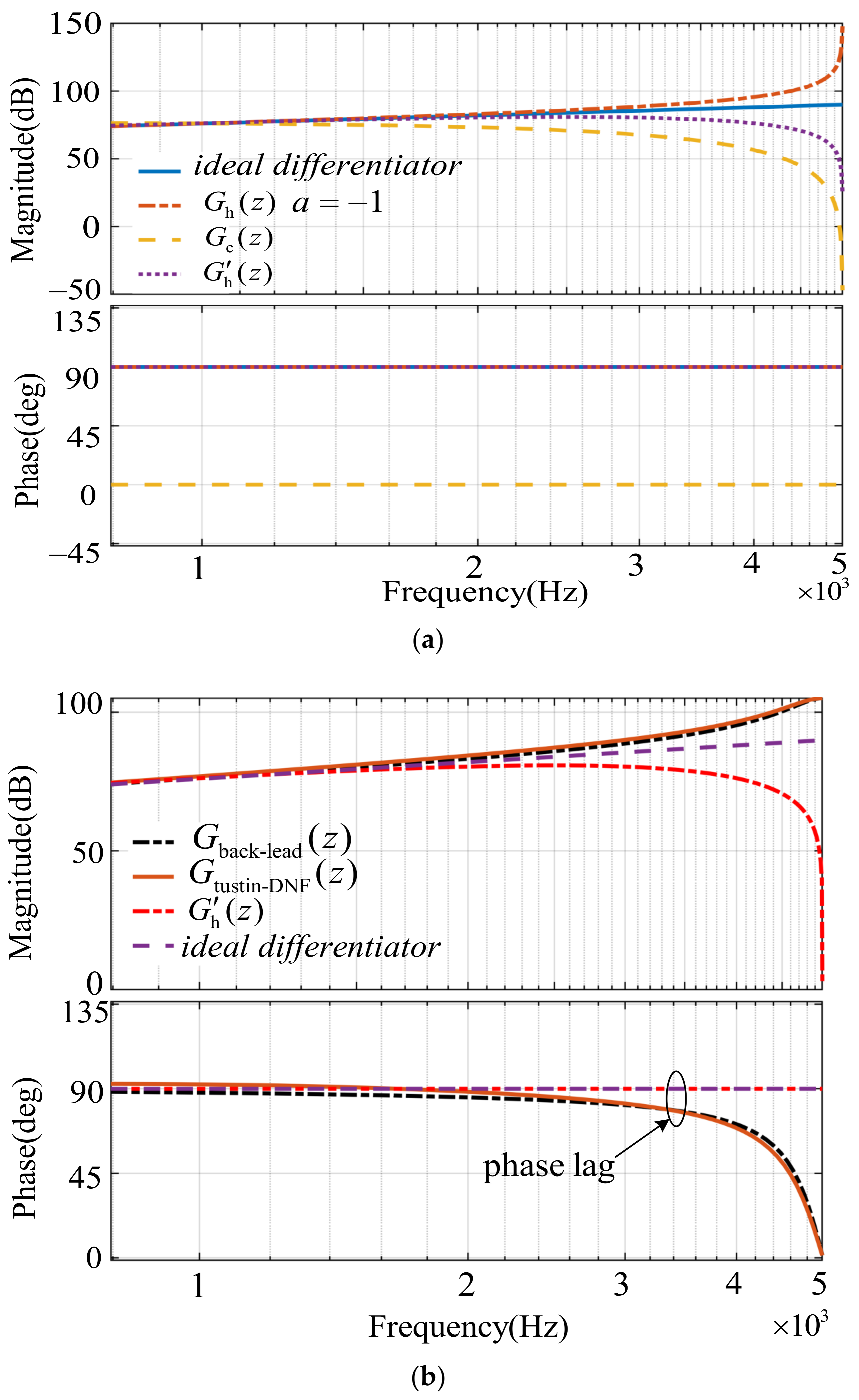
Figure 5 depicts the zero-pole distribution of Gh(z), in which there is a zero z = 1 and a pole z = a, and the pole a slides on the real axis within the range (−1, 1), which corresponds with each different lead phase angle θ within the range (0, π/2). As of Gh(s), the two boundary values 0 and π/2 are not available. However, unlike the Gh(s), the parameter a of Gh(z) can change within an extended range [−1, 1]. Gh(z) simplifies to H and fcrit = fs/6 in the case of a = 1, which is just the conventional CCFAD, and it can be attained that Gh(z) = H (z − 1)/(z + 1) in the case of a = −1, which is similar to the Tustin discrete form of an ideal differentiator. As seen in Figure 6a, the ideal differentiator can provide π/2 phase lead compensation and finite gain over the entire frequency domain, but can not be implemented in practice. On the contrary, Gh(z) (a = −1) can achieve the same phase-lead compensation and be easily realized in the digital-control system, but infinite gain arises at the Nyquist frequency, which is more likely to amplify the figure high-frequency noises. In order to overcome the drawback of Gh(z) (a = −1), this paper proposes a strategy of cascading a digital low-pass filter with it.
A digital low-pass filter is cascaded with Gh(z) (a = −1), aiming to suppress the high-frequency infinite gain of Gh(z) (a = −1) and keep the other frequency characteristics approximately unchanged. The discrete expression of the digital low-pass filter is given as [26]:
where m is an adjustable parameter. Substituting z = esT into (10), the continuous expression of Gc(s) is obtained as (11)
Gc(s) is positive when m ≥ 2 because cos(ωTs) ϵ [−1, 1] and Gc(s) behaves as a variable constant over the whole frequency domain, which means its phase is always zero. In order to ensure the gain stays zero at the Nyquist frequency, let m = 2 and cos(ωsT/2) = −1; hence, T = Ts. The improved discrete form of Gh(z) (a = −1) after cascading Gc(s) is obtained as
For comparison purposes, multiply the several functions in Figure 6 by a different constant to ensure that the magnitude–frequency characteristics are almost the same in the low-frequency band without changing the phase–frequency characteristics. As seen in Figure 6a, obviously, Gc(s) actually is a digital low-pass filter, whose phase keeps zero in the entire frequency band, and it has little effect on the magnitude–frequency characteristic of Gh(z) (a = −1) in the low frequency band after cascading it. However, the gain of Gh(z) (a = −1) in the high frequency band, especially at the Nyquist frequency, is attenuated substantially to below 0 dB, referring to the frequency characteristic curve of . Reference [33] proposes a first-order differentiator based on a backward Euler plus lead compensator and a second-order differentiator based on a Tustin plus digital notch filter to be alternatives of an ideal differentiator, whose transfer functions are marked as Gback-lead(z) and Gtustin-DNF(z), respectively. In addition to and the ideal differentiator, the bode plots of Gback-lead(z) and Gtustin-DNF(z) are also shown in Figure 6b. It is clear that the magnitudes of Gback-lead(z) and Gtustin-DNF(z) are finite and relatively higher compared with the ideal differentiator in the high-frequency domain, and the magnitude of is almost flattened in the entire frequency range except for approximate 0 dB at the Nyquist frequency, implying better disturbance rejection ability. The phases of Gback-lead(z) and Gtustin-DNF(z) are almost the same, with a slight lag in the mid- and high-frequency domain compared with the ideal differentiator. However, the phase frequency characteristic of is totally identical to that of the ideal differentiator. Based on the analysis above, it is concluded that is the closest match with the ideal differentiator in terms of frequency characteristics. In addition, the EDR obtained is [0, fcrit] (fcrit < fs/3) using the proposed method in [33] due to the phase lag in the mid- and high- frequency domain, while the EDR obtained is [0, fs/3] using the proposed method in this paper. The feature comparisons of different digital compensation methods are listed in Table 1.
For the theoretical analysis simplicity, only using Gh(z) without considering the correction link Gc(z) is sufficient in analyzing the system stability and introducing the design procedure of the digital controller and damper in the following.
3.2. System Discretization
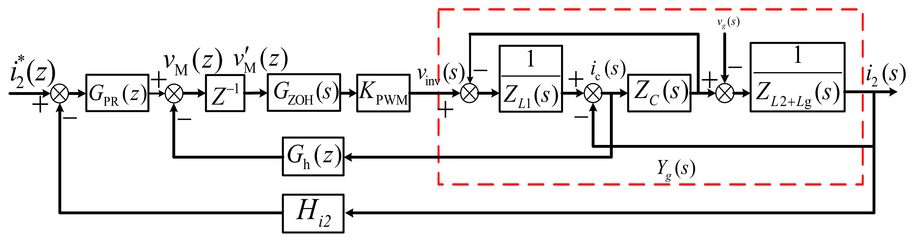
System analysis based on impedance equivalence is done in the s-domain, which is appropriate with the discrete controller not included. To co-design the discrete current controller and active damper, it is more accurately done in the z-domain. The continuous system model in Figure 2 is transformed into a discrete one, shown in Figure 7.
Digital pulse width modulation (DPWM) is modeled as a zero-order holder (ZOH) with half a period delay, which is proven to be an appropriate approximation of the uniformly sampled DPWM [40]. The next block is the z−1 delay block which represents a period computation delay. The transfer function Yg(s) representing the LCL filter is given in (13) and its discrete counterpart showed in (14), respectively.
where GZOH = (1 − e−sTs)/s denotes the transfer function of the ZOH. After applying Tustin transformation, the discrete expression of the PR current controller GPR(s) in (1) can be obtained shown in (15).
According to (9), (14) and (15), the expression of the transfer function for the dual-loop control scheme can be derived as follows:
From (16), it can be concluded that there is no nonlinear link like transcendental functions in z-domain compared with that in s-domain. The eigenvalues can thus be solved simply, hence obtaining the condition of including RHP poles in TD(z).
4. System Stability Analysis
System stability needs to be further analyzed for the cases of different resonant frequencies after introducing the feedback link Gh(z) = H(z − 1)/(z + 1). Reference (16) can be redrawn as (17).
where GPR(z) has two conjugate poles on the unit circle that does not belong to the right-half plane. To judge whether the system has the RHP poles, the poles distribution of TD(z), more accurately, the roots distribution of denominator D(z) of TD(z) whose expression is given in (18) should be analyzed.
According to the Routh criterion, the number of RHP poles of (16) is equivalent to the changing times of the first-column elements [a0 a1 b1 c1 a4] of (A2) in Appendix A being positive or negative. Considering fr < fs/2, then ωrTs < π and a0 > 0, a4 > 0, and assuming that a1 b1 c1 are all above zero, parameter H must satisfy the following three requirements shown in (22).
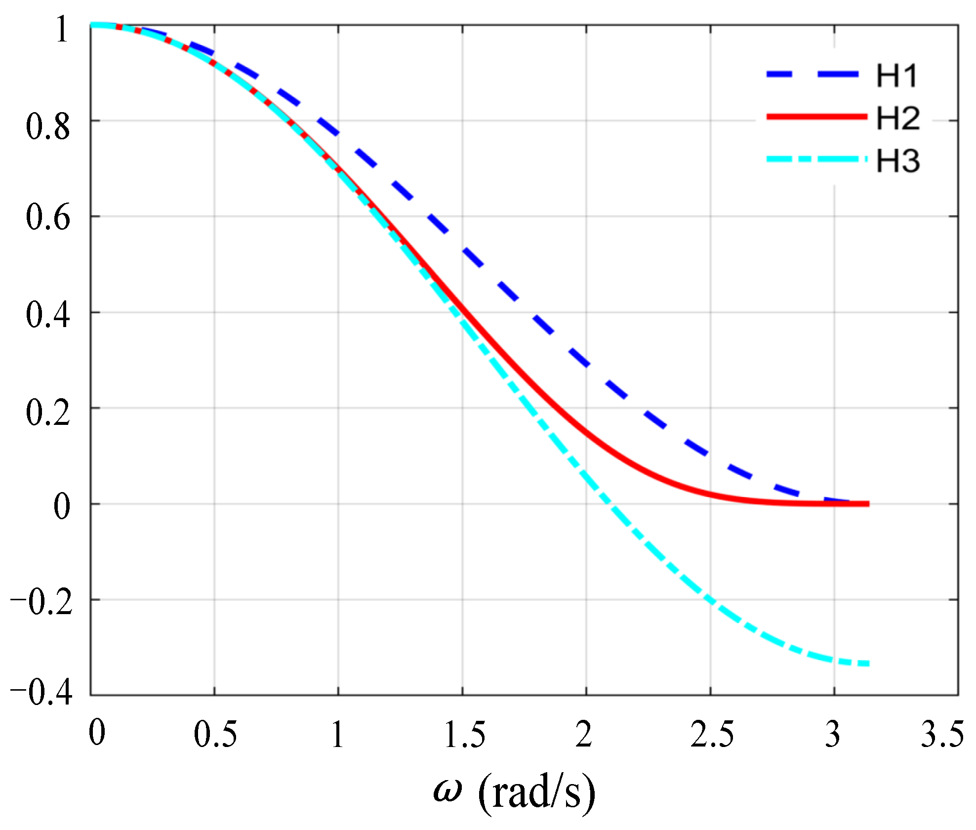
The parameter H must satisfy the following three requirements shown in (19) by conducting the Routh criterion on D(z). When ωrTs ranges (0,π), the second parts of the functions H1, H2, H3 in (19) are plotted in Figure 8, in which it can be concluded that H3 < H2 < H1.
The relationship between the value range of H and the number of RHP poles of the system is listed in detail in Table 2.
For analysis simplicity, only the case H > 0 is studied in this paper. From Table 2, it is observed that the system has no RHP poles when H < H3, whereas there are two RHP poles when H > H3. Therefore, H3 is the critical value and the critical frequency fcrit = fs/3 can be solved when H3 = 0, which just matches the critical frequency fcrit (a = −1) in the analysis of virtual resistance in the previous section. It is concluded that the condition of the system applying the feedback link Gh(z) = H(z − 1)/(z + 1) with no RHP poles is fr’ < fcrit; in other words, Req(ω) is positive at the frequency below fcrit.
For convenience, the method proposed in this paper is called Method 1 and the CCFAD is called Method 2. The compared analysis of the two methods is presented in the following.
The system in z-domain is commonly evaluated with the Nyquist stability criterion, i.e., P = 2(N+ − N−), where P denotes the number of the open-loop RHP poles, and N+ and N- denote the numbers of positive and negative −180° crossings, respectively. It would be counted as one positive or negative crossing as long as the gain is above 0 dB when the phase transits the −180°.
Based on the previous analysis, the critical frequencies fcrit are fs/6 and fs/3 for method 1 and method 2, respectively; as a result, the stability requirement of the two methods are different. As listed in Table 3, the cases are classified in terms of the frequency band on which the equivalent resonant frequency fr’ is located. As for the method 1, when fr’ < fs/6, Req(fr’) is positive, i.e., there are no RHP poles and just one negative −180° crossing at fr; when fr’ > fs/6, Req(fr’) is negative, i.e., there are two RHP poles and −180° crossing at fr and fs/6, respectively. Here, GM1 and GM2 represent the gain margin at fr and fs/6, respectively. Especially, when fr’= fs/6, Req(fr’) is negative and there is no −180° crossing, which leads to system instability due to the fact that the requirements of GM1 and GM2 cannot be met simultaneously. As for method 2, when fr’ < fs/3, Req(fr’) is positive, i.e., there are no RHP poles and just one negative −180°crossing at f1; when fr’ ≥ fs/3, Req(fr’) is negative, i.e., there are two RHP poles and −180°crossing at f1 and f2, respectively. Here, GM1 and GM2 represent the gain margin at f1 and f2, respectively.
As listed in Table 3, for either method 1 or method 2, when fr’ < fcrit, the gain margin is required to be above 0 dB. On the contrary, the gain margin requirement is more stringent when fr’ > fcrit; therefore, a larger EDR, and in other words, a larger fcrit, is desirable.
In a weak grid, the grid impedance Lg is variable, which leads to the variation of fr, hence weakening the system robust stability. The compared analysis of the two methods under Lg variation is presented in the following.
Parameters used for simulation and experiment are given in Table 4, where two different capacitor values are chosen to generate different filter resonance frequencies on the condition that convert-side inductance L1 and grid-side inductance L2 are selected unchanged. For the weak grid, the grid inductance Lg may change from zero to the maximum value available, which is chosen corresponding to the short circuit ratio (SCR) of 10 [5]. Compared with the inductance, the commercial capacitors are more accurate and well-tested; therefore, changing the capacitor’s value for analysis is a preferable choice to inductance value.
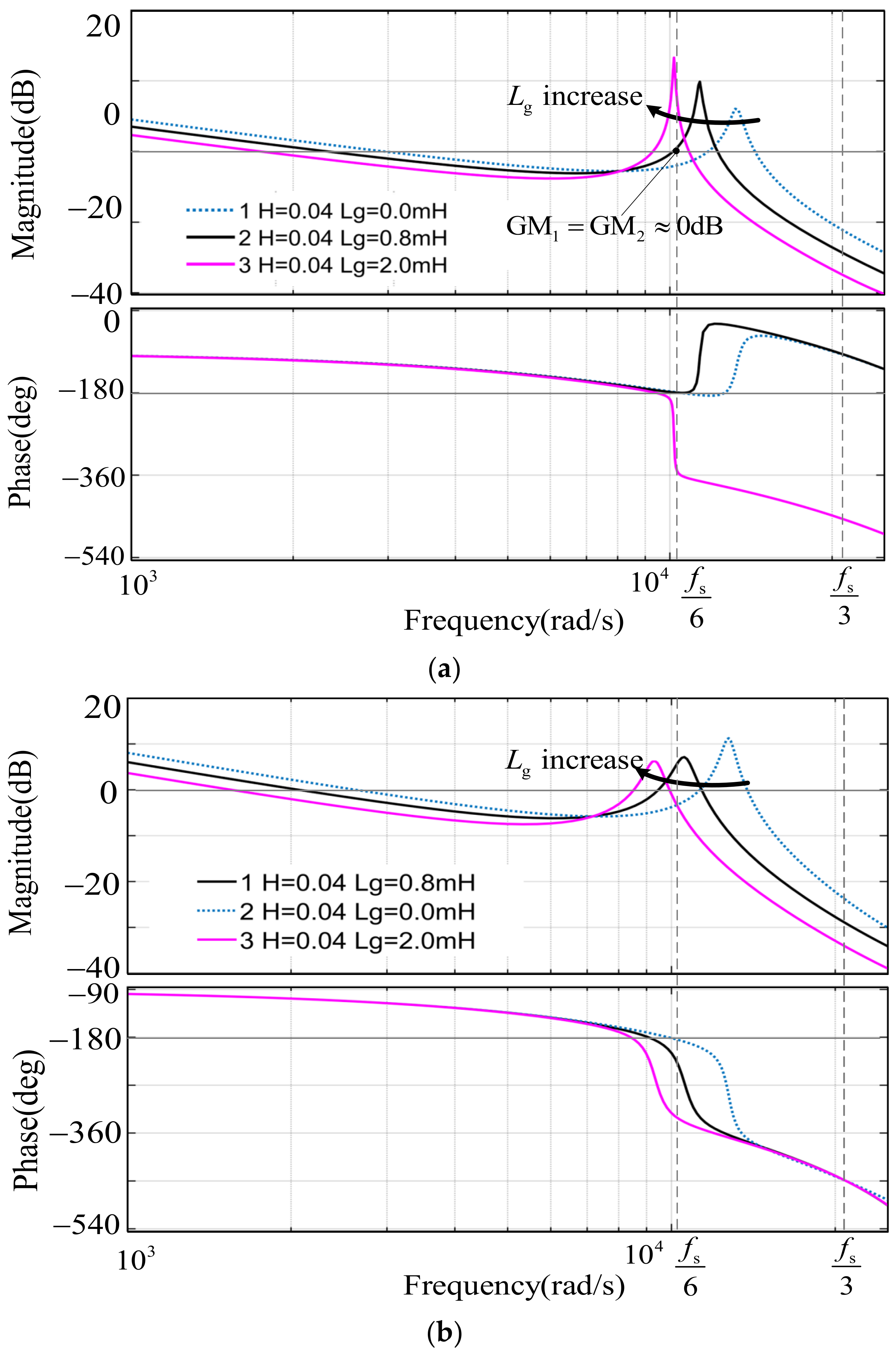
Figure 9 illustrates the frequency response of the two methods mentioned above, which is affected by the variation of the grid inductance Lg. For the case C = 9.4 μF and Lg = 0 mH, the original resonant frequency fr is equal to 2.01 kHz, which is a little above and close to fs/6. As shown in Figure 9a, when method 1, namely Gh(z) = H, is applied, referring to the curve 1, the forward-path phase transits through −180° at fs/6 and fr, respectively. The requirement of the gain margin GM1 < 0 at fs/6 and GM2 > 0 at fr must be met to ensure the system stability according to the Nyquist stability criterion. When Lg varies from 0 mH to 0.8 mH dynamically, the actual fr will get closer to and finally be approximately equal to fs/6. Obviously, it can be seen from curve 2 in the plot that the two frequency points fs/6 and fr are so close (almost overlap) that the requirement of the gain margin GM1 and GM2 cannot be met simultaneously or the value of GM1 and GM2 are not adequate to ensure system robust stability. When Lg increases further up to 2.0 mH, fr thus shifts below and away from fs/6. The forward-path phase transits through −180° only at fr, and the system goes back to the stability state again in case the requirements for PM and GM1 are met simultaneously, as illustrated by curve 3 in the plot. As shown in Figure 9b, when method 2, namely Gh(z) = H(z − 1)/(z + 1) is applied and Lg varies within the range (0, 2 mH), the forward-path phase transits through −180° once at the frequency below fs/3, for which the system stability can be guaranteed only when the requirements for PM and GM1 are met simultaneously.
For the case C = 3.9 μF and Lg = 0 mH, the resonant frequency fr is equal to 3.12 kHz, which is a little below and close to fs/3. Applying method 2, referring to Table 2, when the coefficient H < H3 mentioned in the previous section, Req(fr’) is positive and the forward-path phase transits through −180° only at the frequency f1; when the coefficient H > H3, Req(fr’) is negative and the forward-path phase transits through −180° at f1 and f2, respectively, as illustrated by curve 2 and curve 1 in Figure 9c. However, one crossing point through −180° will be gone and curve 1 turns into curve 3 (Lg = 2.0 mH) eventually when Lg changes from 0 to 2 mH.
To summarize the above analysis, it can come to some conclusions as follows:
For the active damping method with Gh(z) = H, an issue that the system will be unstable or have low robustness when the two −180°crossing points fr and fs/6 almost overlap is likely to arise due to the variable grid inductance Lg; this is inevitable in the weak grid.
For the active damping method with Gh(z) = H(z − 1)/(z + 1) whose effects on the system can be divided into two parts: (z − 1)/(z + 1) and H, the first part decides the critical frequency fs/3 is much above fs/6; hence, there just exists one −180° crossing point when fr’ is lower than fs/3, which is easier to satisfy the system stability requirements. Moreover, it is worth noting that f1 < fs/6 and f2 > fs/3 due to phase compensation at fs/6 and fs/3 caused by Gh(z). For example, the phase compensation angle is π/2 at fr referring to (20) obtained by substituting z = ejωrTs into (17). In the meantime, through tuning the second part H, the appropriate damping and sufficient stability margin can be achieved.
where Kp denotes the proportional efficiency of the PR controller, which can simplify to Kp in the frequency region above the cut-off frequency fc.
5. Co-Design of the Active Damper and Current Controller
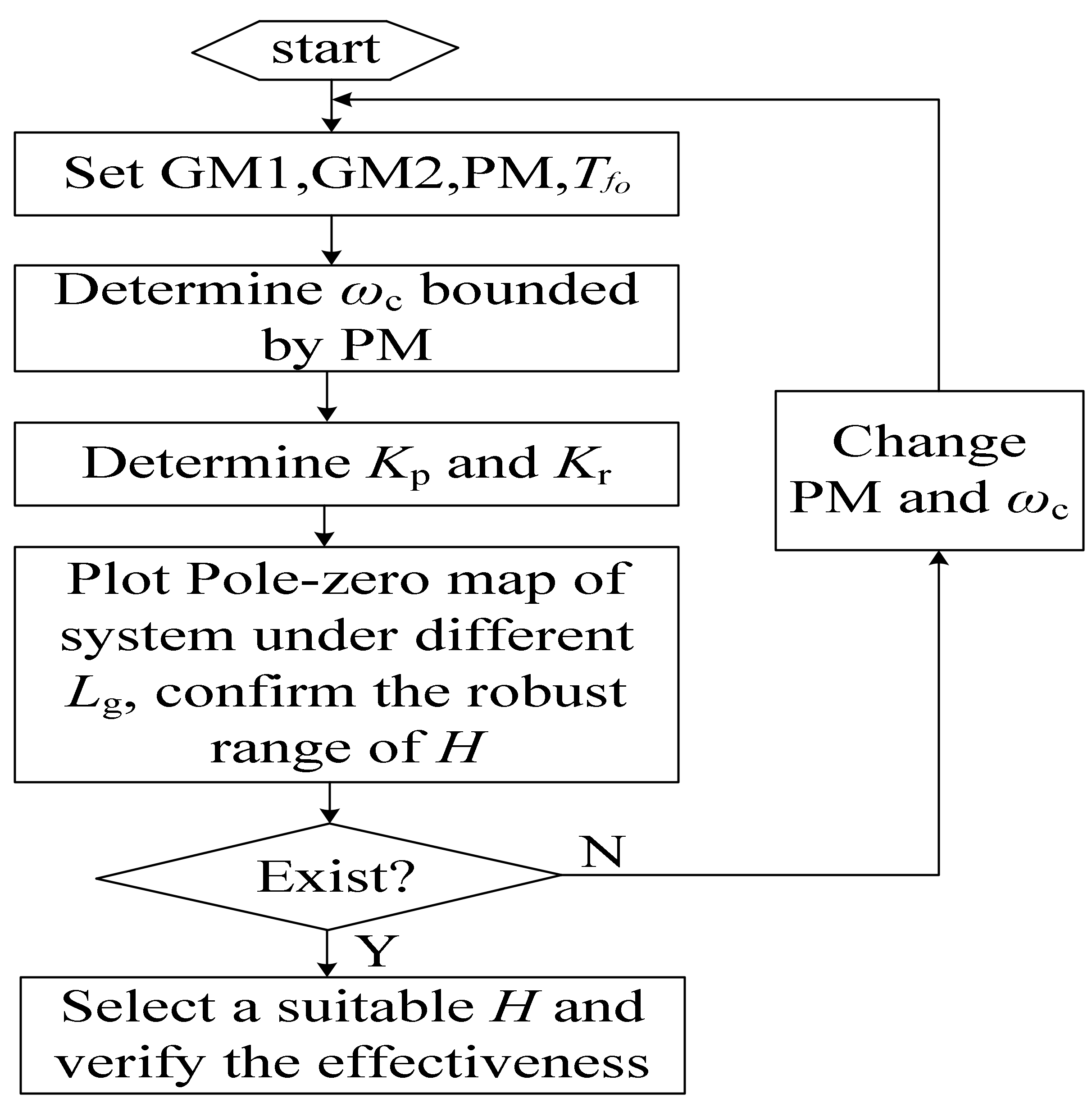
The conventional approach to the design and control system with an active damper is to design the current controller first and then design the active damper, which has ignored the virtual impedance effect on current controller. A reasonable design procedure for the overall control strategy is to co-design the current controller and the active damper simultaneously using root locus or other analytical techniques. Therefore, the approach proposed in this paper is that the constraint of the system stability margin requirement on H is derived first followed by the constraint of the variable grid impedance Lg on H, and the suitable H is finally selected after considering all constraints.
According to Figure 2, the expression of the open-loop transfer function of the system model in the s-domain can be obtained.
where the expression of Gh(s) is given as (22) by substituting the z = esTs into Gh(s).
When analyzing the amplitude frequency characteristic of TD(s), the filter capacitor can be neglected below the cut-off frequency fc due to its reactance being far higher than that of the grid-side inductance, and GPR(s) can be simplified to KP at fc and KP + Kr at fundamental frequency fo. Therefore, (23) and (24) can be obtained by substituting s = j2πfc and s = j2πfo into (21), respectively.
KP and Kr can be solved from (23) and (24), whose expressions can be given as follows:
It is noted that (26) shows the constraint on Kr for a given Tfo. According to the definition of phase margin PM, the expression of PM can be written as
When analyzing the phase frequency characteristic of TD(s), GPR(s) can be simplified to KP + 2 Krωi/s at fc. Substituting GPR(s) = KP + 2 Krωi/s into (27), (28) is obtained.
By substituting (25) and (26) into (28) and doing some simple mathematical operations, (29) and (30) are obtained.
For a given ωc, (29) shows the constraint on Kr for a given PM, and for a given Kr, (30) depicts the value range available of H and ωc.
In order to obtain the constraint of the gain margin GM on H, the crossing frequencies f1 and f2 should be solved first. However, different from the CCFAD whose crossing frequencies are fixed at fs/6 and fr, it is hard to obtain the solution of f1 and f2 from (31) due to the crossing frequencies f1 and f2 for the proposed method varying with H. According to the definition of GM, (32) is deduced, which denotes that for given H, the corresponding frequency points satisfy the design requirement of GM.
The key to co-designing the current controller and active damper is the determination method of their parameters whose value ranges can be obtained according to the constraint formulas mentioned above and given system stability requirements. A simple determination procedure of the parameters recommended will be given below, which takes the case of C = 3.9 μF and the remaining parameters listed in Table 2 as an example.
(1) Give the system stability requirements to ensure system robust stability. It is commonly claimed that PM > π/4 for better dynamic performance and Tfo > 50 dB for lower grid-tied current amplitude error as the grid fundamental frequency fluctuates; besides, for adequate system robustness, GM1 = 3 dB at f1 and GM2 = −3 dB at f2 if f2 exists.
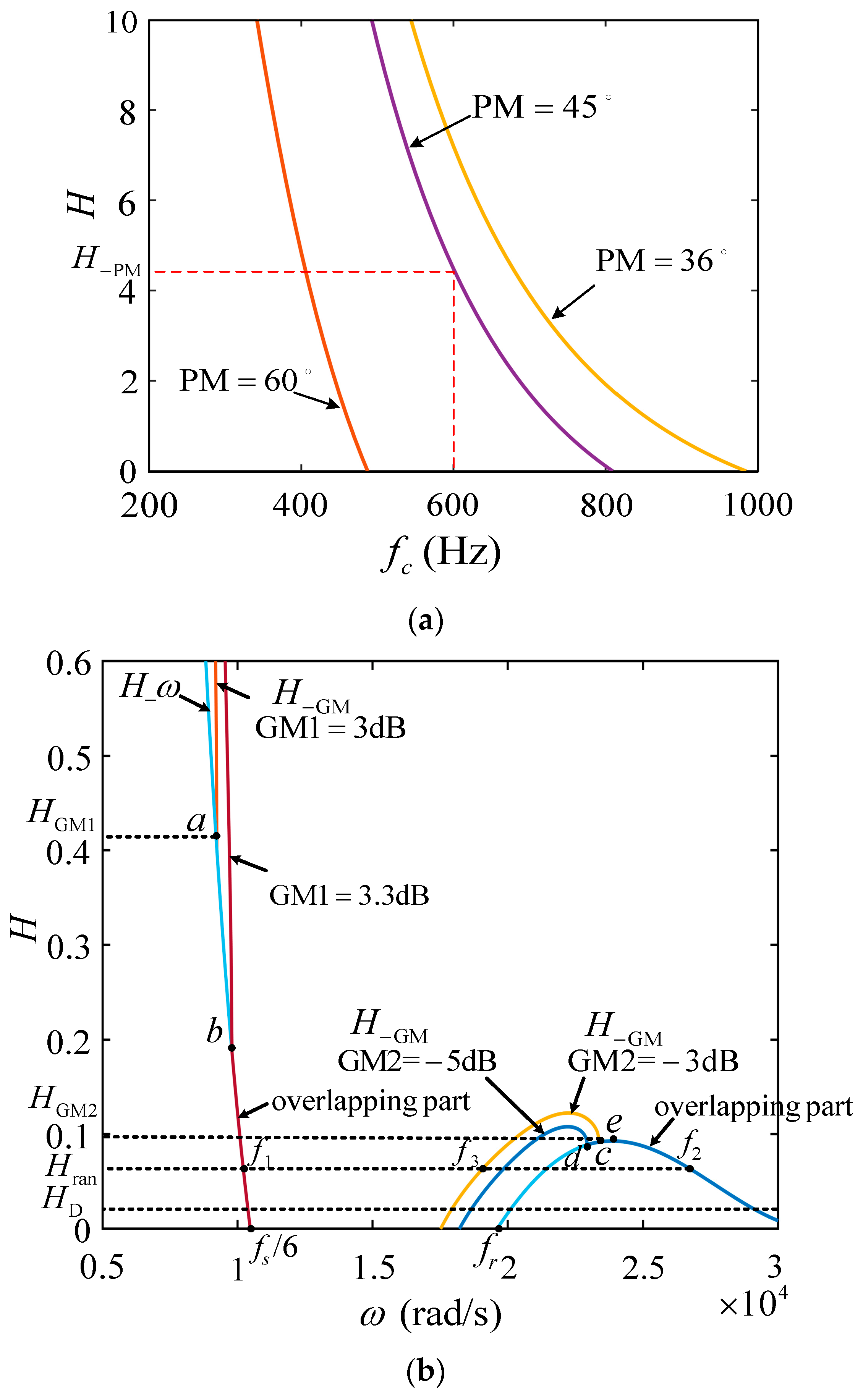
(2) Identify the resonant frequency ωc without taking Lg into account. According to the fact that the higher fc, the better the system dynamic performance, and considering that fs in the experiment in this paper is not high, the value range available of fc is the left side of the curve PM = π/4 shown in Figure 10a, and fc = 600 Hz is chosen.
(3) After selecting fc, Kp is decided by (25) and Kr is chosen in the value range available decided by (26) and (29), which give the lower limit value and upper limit value, respectively. Kp = 0.05 and Kr = 75 are selected in this paper.
(4) A bounded range for H can be determined by some constraints outlined earlier. Substitute fc = 600 Hz and GM1 and GM2 with different values into (32) to get different curves, as shown in Figure 10b. The curves in Figure 10b are divided into left and right parts according to frequency range. In the left half plane of Figure 10b, the curve H_ω and two H_GM curves representing GM1 = 3 dB and GM1 = 3.3 dB overlap after point a and point b from left to right, respectively, where the overlapping part means that the two curves H_ω and H_GM have common solutions of H and f1 on the condition that the requirement for GM1 is met, and it can be seen that the intersection point moves to the right when the value of GM1 increases, which indicates that the range value available of H gets smaller accordingly. Therefore, the H_GM1 corresponding to point a is the maximum value in the case of GM1 ≥ 3 dB. In the right half plane of Figure 10b, the curve H_ω and two H_GM curves representing GM2 = −3 dB and GM1 = −5 dB, respectively, overlap after point c and point d from left to right, respectively, where the overlapping part means that the two curves H_ω and H_GM have common solutions of H and f2 on the condition that the requirement for GM2 is met, and the intersection point moves to the right when the value of GM2 increases. Therefore, the H corresponding to point e is the maximum value in the case of GM2 ≥ −3 dB. Based on the above analysis, obviously, under the condition that the requirements for GM1 and GM2 are met simultaneously, the value range of H is [HD, H_GM2], in which the frequency points f1, f2, and f3 corresponding to any Hran are consistent with that shown in the Figure 9c.
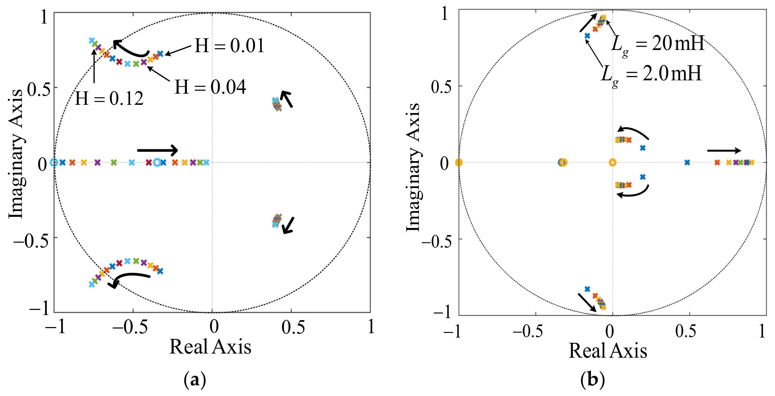
(5) Except for the value range limitations mentioned in (4), the determination of the best possible damping gain H requires one more consideration, which is to place the two resonant poles of system as far as possible inside the unit circle to achieve the maximum damping. A pole-zero map strategy is used to determine the selection of H in Figure 11a. Based on all consideration above, for the example system, a better choice of H occurs when H = 0.04 marked in Figure 11a.
(6) Figure 11b demonstrates the feasibility of the choice of H when Lg changes from 0 to maximum value (0.1 pu). It is clear that the resonant poles are always inside the unit circle, which indicates that the system stability margin can be guaranteed all the time. Otherwise, return to (2) and reselect another fc.
Based on the above analysis, the flowchart of the design procedure can be drawn as shown in Figure 12.
6. Verification
In order to verify the correctness of the theoretical analysis in Section 4 and Section 5, simulations and experiments are conducted with the parameters listed in Table 4.
6.1. Simulation Results
A simulation model of a three-phase LCL grid-connected inverter system was built using Matlab/Simulink simulation platform, which was conducted with the parameters listed in Table 4.
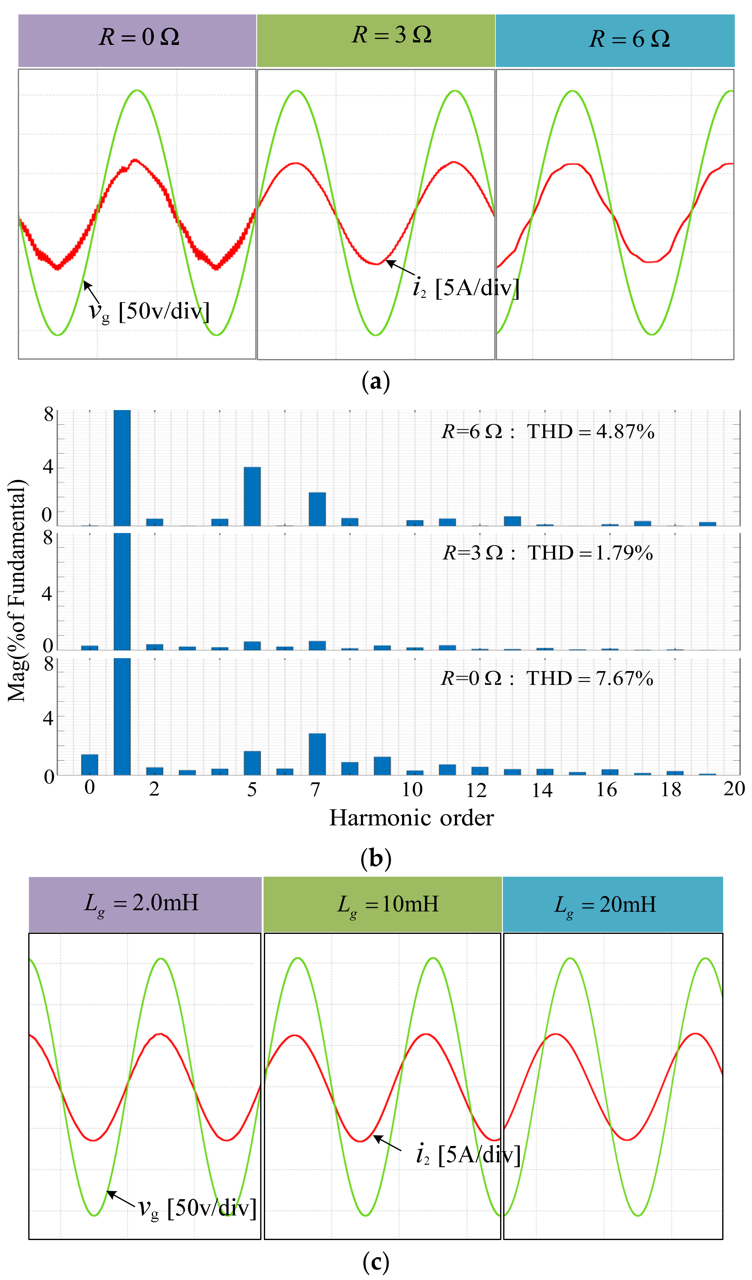
The impedance of the power grid consists of resistance and inductance when the system is in the medium- and low-voltage distribution networks. Using the proposed method, choose H = 0.1 while keeping the power grid inductance Lg = 2.0 mH unchanged, and run simulations with varied power grid resistance values, i.e., varying reactance to resistance ratios Xg/Rg. According to the simulation results, the grid resistance R progressively increases from zero, and the resonance and THD of the grid current change. When R = 0 Ω, the grid current experiences a slight resonance, the high-frequency signal is amplified, and the THD increases. Because of the damping effect of resistance, as R grows, the grid current’s resonance reduces gradually, and the THD steadily falls. As R grows further, the content of the grid current low-order harmonics, notably the 5th and 7th harmonics, increases, causing a gradual rise in the THD. As a result, the system may become unstable. To ensure system stability in this instance, extra hardware changes and software control are required to obtain a suitable Xg/Rg. Figure 13a,b, respectively, provide simulation results and THD analysis results of grid current waveform with different R values, namely 0 Ω, 3 Ω, and 6 Ω. In order to better verify the harmonic suppression ability of the algorithm, the worst-case conditions are considered, assuming that the grid impedance is purely inductive, i.e., R = 0 Ω.
In addition, according to the analysis in the previous section, using the proposed method, H = 0.4 is selected for simulation under different grid inductance conditions. Figure 13c shows the simulation results under Lg = 2.0 mH, Lg = 10 mH, and Lg = 20 mH, which correspond to SCR =10, SCR =2, and SCR =1, respectively. As can be seen, the grid current is stable in three cases and the results is consistent with Figure 12b, which means that the design procedure is effective and indicates that the system can stably operate in ultraweak grid.
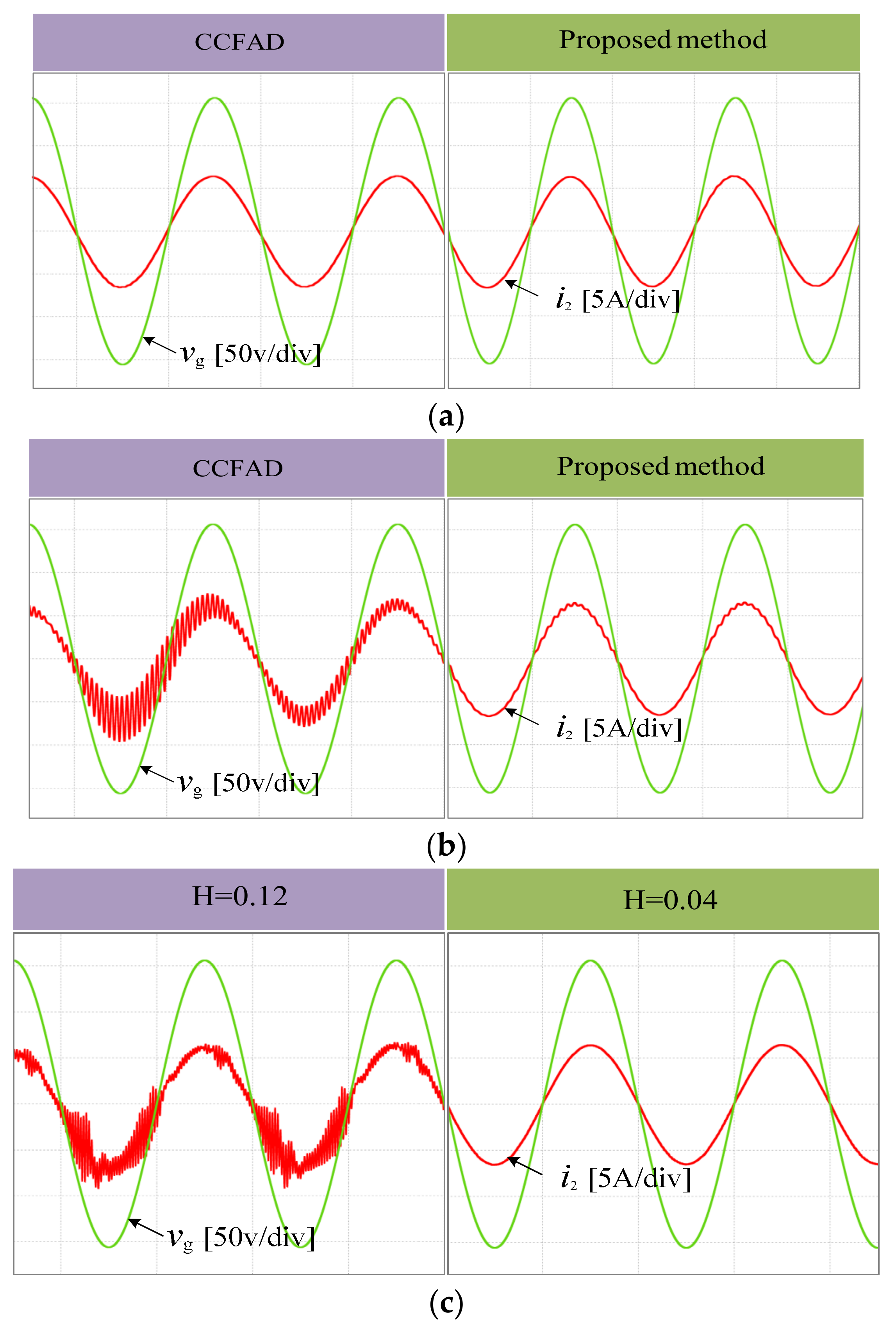
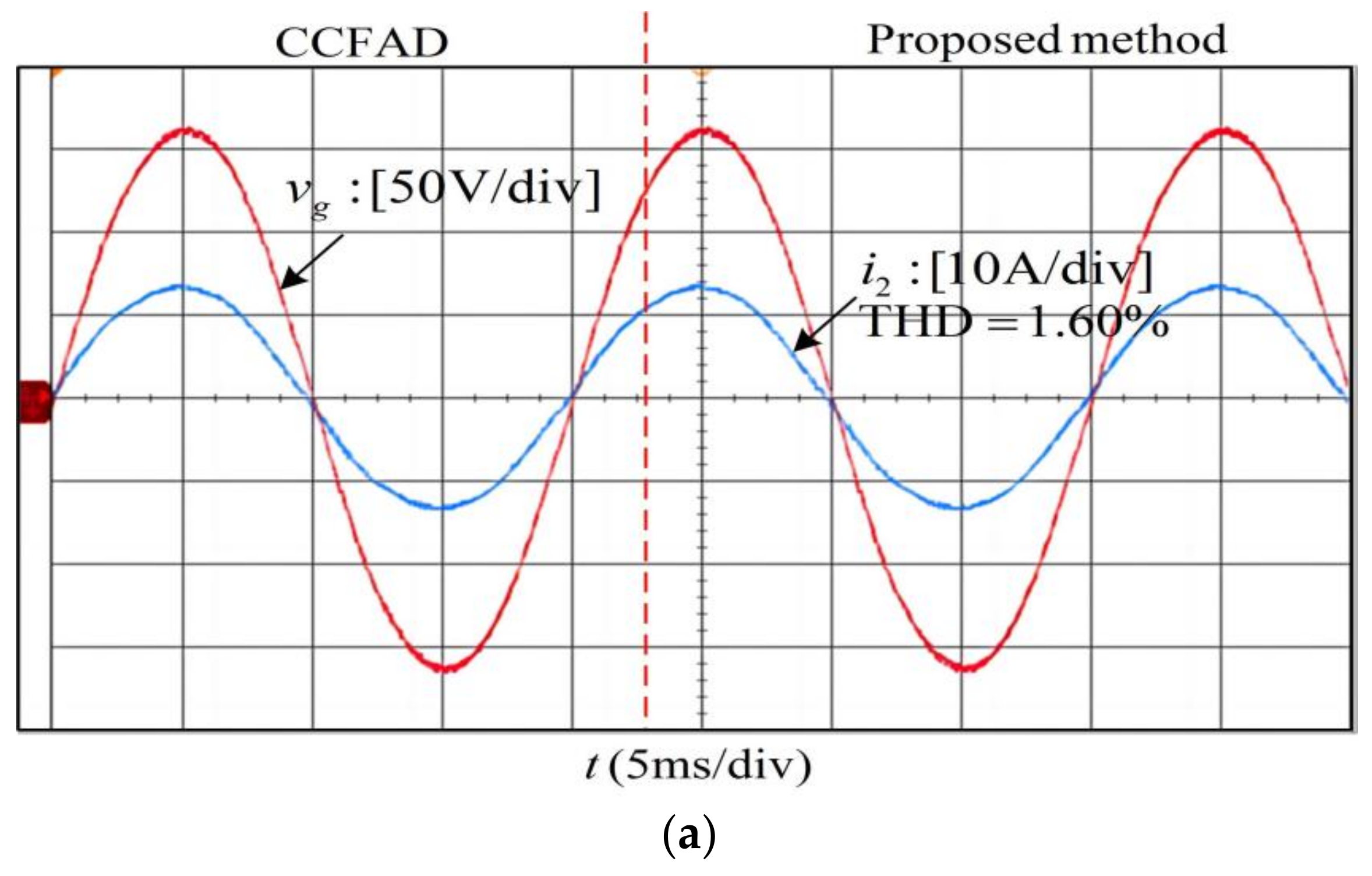
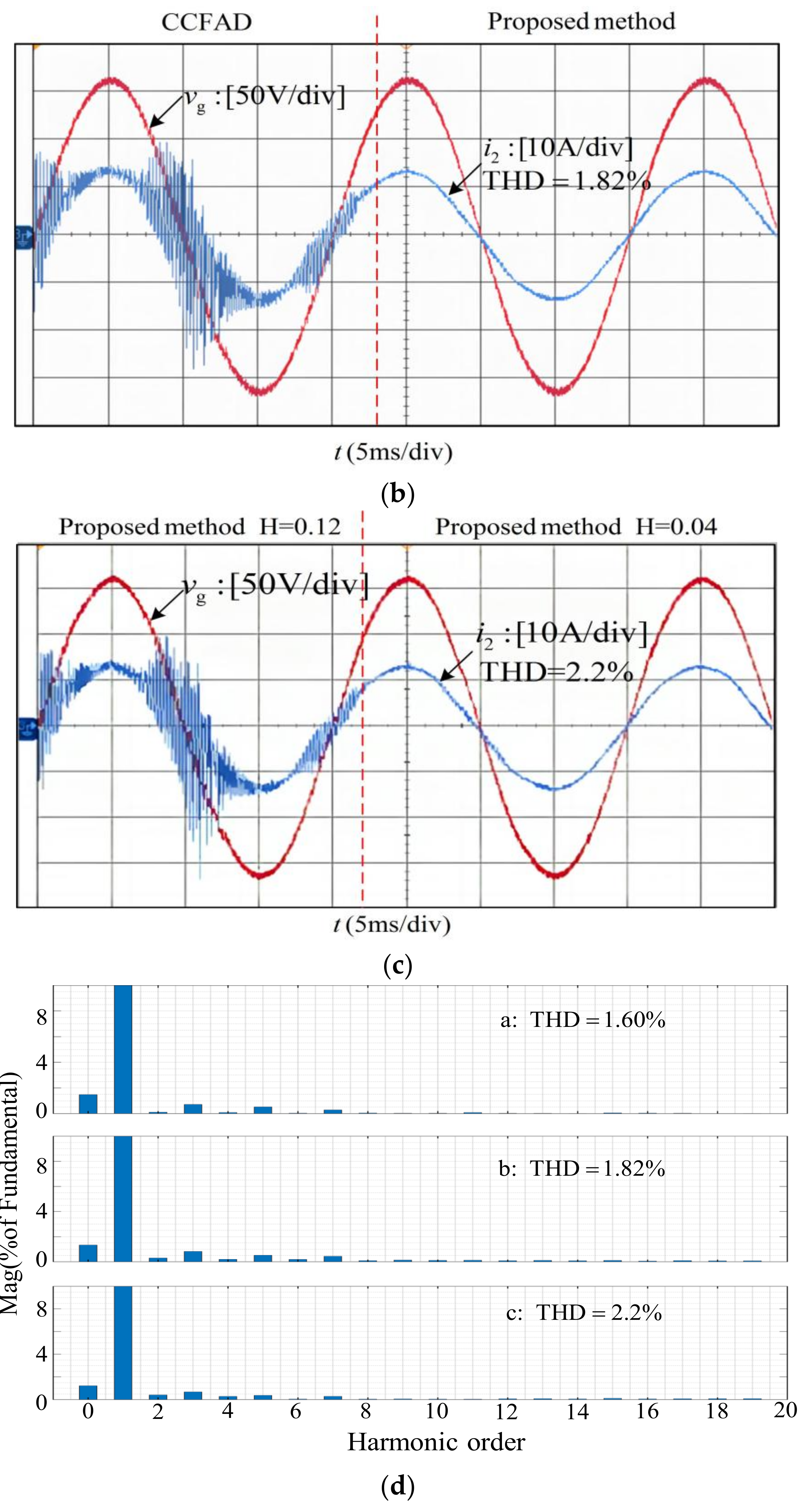
The simulation is conducted with the controller parameters Kp = 0.05 and Kr = 75. Figure 14 shows the comparison results between the proposed method and CCFAD. As can be seen, in the case of Lg = 2.0 mH and C = 9.4 μF, the filter resonant frequency fr = 1.49 KHz is smaller than fs/6, which is within the EDR of the two methods. By setting the controller parameters reasonably, resonance will not occur in the grid current. As shown in Figure 14a, after using the proposed method, there was no significant change in the grid current and the system was in a stable state. In the case of Lg = 0.8 mH and C = 9.4 μF, the filter resonant frequency fr = 1.68 KHz is approximately equal to fs/6. At this time, no matter how to adjust the control parameters, CCFAD cannot meet the requirements of two magnitude margins at the same time, so the system is in a marginal stability state. However, the resonance frequency fr is within the EDR range when using the proposed method. To ensure system stability while designing parameters, just the requirement for GM1 must be satisfied. As shown in Figure 14b, there is a slight resonance in the grid current on the left, but after adopting the proposed method, the resonance in the grid current on the right disappears. In the case of C = 3.9 μF and Lg = 0 mH, the filter resonant frequency fr = 3.12 KHz is slightly less than fs/3, so it is in the EDR of the proposed method. When the proportional feedback coefficient H of the damping loop is changed from 0.12 to 0.04, according to Figure 12a, it can be seen that the positions of the two resonant poles of the system enter the unit circle from outside, indicating that the system transitions from unstable to stable. Figure 14c shows that the resonance in the grid-connected current disappears, and the simulation results agree with that depicted in Figure 12b.
6.2. Experimental Results
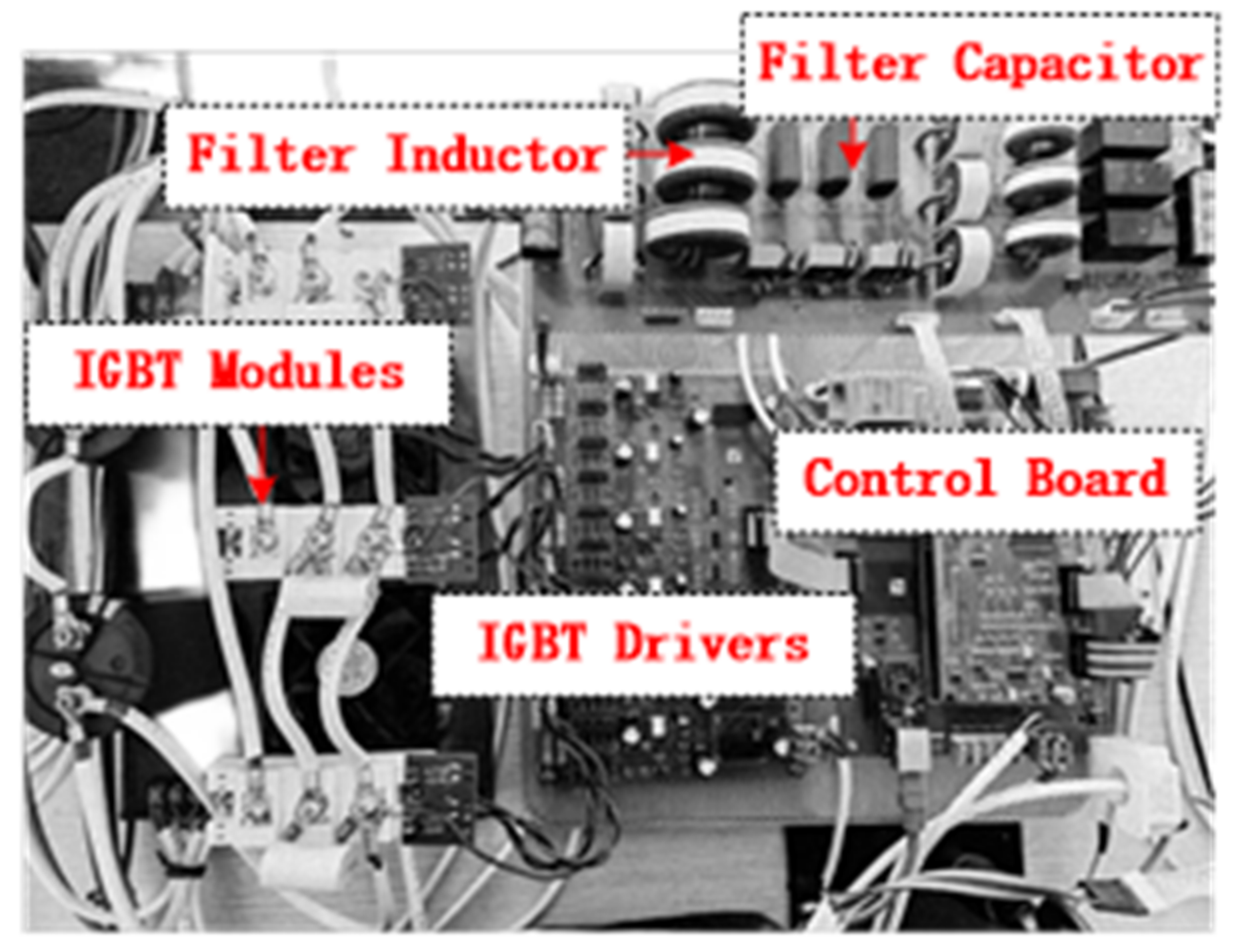
An experimental platform of 6 kVA three-phase, grid-tied inverter is built, for which the system parameters are shown in Table 3. Figure 15 shows the prototype photograph. We use TMS320F28035 chip of TI company to process digital signals, and use INFINEON’s FF50R12RT4 IGBT as the power switch. Also, a programmable AC source (TPV7006S) series inductance is used to simulate the actual power grid. The steady state and load jump test waveforms of grid-tied inverter are given below.
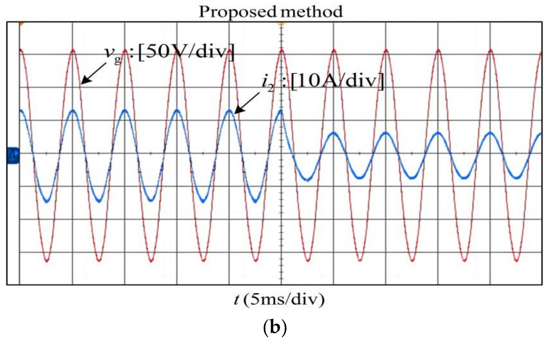
The experiments adopt the same controller parameters as the simulation. For the convenience of direct comparison, the experiments in Figure 16a,b are conducted by switching between the two methods, and those in Figure 16c are done by manually changing from 0.12 to 0.04 in the parameter H using the proposed method. It can be observed that the experimental waveforms are basically consistent with the simulation results. Besides, it should be pointed out that each individual harmonic distortion and the measured total harmonic distortion (THD) shown in Figure 16d all meet the distortion limits in IEEE Standard 519-2014 [41].
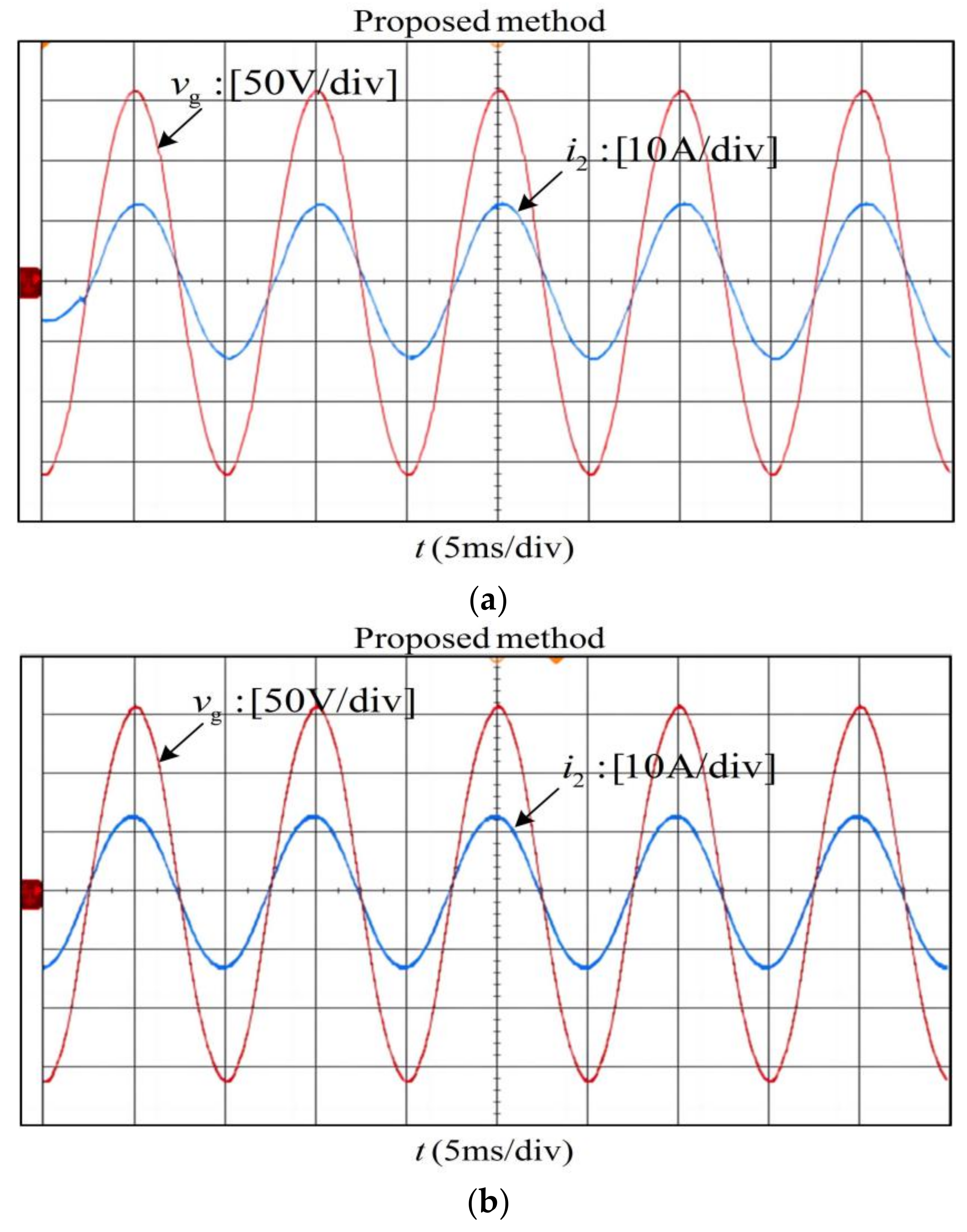
Figure 17 shows the experimental results of phase-A with the proposed method in the case of the Lg = 0 mH and Lg = 2.0 mH. The experimental result agrees with that depicted in Figure 12b. Combining the experimental results in Figure 16, it can be summarized that the system using the proposed method can maintain stable operation and exhibit a good damping effect under the condition that the grid impedance is within the range of 0~2 mH, indicating that the system has good robustness to the grid impedance.
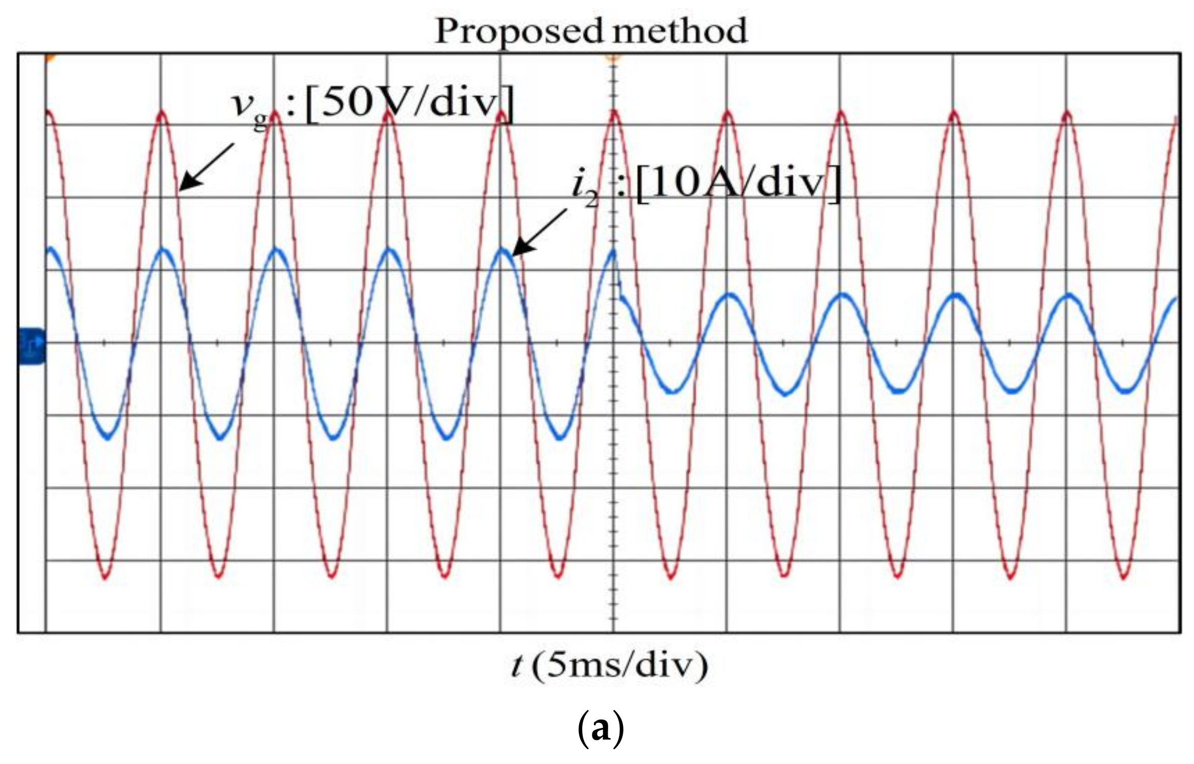
Finally, Figure 18 shows the transient experimental results when the current reference changes based on different Lg. The instantaneous overshoot and adjustment time are both very small, indicating that the new method has good dynamic performance.
7. Conclusions
For the digital control LCL-type grid-tie inverter system, its digital control delay will reduce the system’s robustness to the grid impedance, which may lead to system instability. The article proposes an improved digital differentiator, which can be proven to be a better way to achieve an ideal differentiator. Compared with the ideal differentiator, it has identical phase frequency characteristics that can ensure that the system EDR reaches [0, fs/3] and has better noise rejection capability. In addition, due to their direct discrete nature, compact expressions, and simple algebraic operations, they are more attractive. The tested results from the experiments verified that the proposed active damping method maintains stable operation in weak grids, obtaining high robustness against grid impedance variation. The proposed method emulates the ideal differentiator and increases EDR, which is still relatively small. Future research will focus on further improving EDR.
Author Contributions
Methodology, S.K.; Software, S.K.; Writing—original draft, S.K.; Supervision, Y.L. All authors have read and agreed to the published version of the manuscript.
Funding
This research received no external funding.
Institutional Review Board Statement
This study does not involve humans or animals.
Informed Consent Statement
Informed consent was obtained from all subjects involved in the study.
Data Availability Statement
Data is contained within this article.
Conflicts of Interest
The authors declare no conflict of interest.
Abbreviation
| effective damping region | EDR |
| capacitor current feedback active damping | CCFAD |
| The nonideal generalized integrator | nGI |
| voltage-source inverter | VSI |
| proportional plus resonance | PR |
| right half-plane poles | RHP |
| zero-order holder | ZOH |
| Digital pulse width modulation | DPWM |
| short circuit ratio | SCR |
| Magnitude Margin | GM |
| Phase Margin | PM |
| Total harmonic distortion | THD |
Parameters Nomenclature
| KP | the proportional coefficients of the PR controller |
| Kr | the resonant coefficients of the PR controller |
| ωi | the −3 dB bandwidth cut-off angle frequency of the PR controller |
| ωo | the fundamental angle frequency |
| fo | the fundamental frequency |
| ωc | the cut-off angle frequency of the system |
| Ts | the system sampling period |
| fs | the system sampling frequency |
| Kd | the gain of HPF |
| ωd | the cut-off angle frequency of the HPF |
| A | the modulus of the HPF |
| θ | the lead-phase angle |
| ωr | the resonant angle frequency of LCL-type inverter |
| ω′ r | the system resonant angle frequency |
| f′ r | the system resonant frequency |
| m | the adjustable parameter of the digital low-pass filter |
| H | the constant feedback coefficient |
| Tfo | the gain at the fundamental frequency |
| PM | the Phase Margin |
| GM | the Magnitude Margin |
| Vo | the inverter output phase voltage |
| fsw | the switching frequency |
| Vdc | the DC-link voltage |
| L1 | the converter-side filter inductance |
| L2 | the grid-side filter inductance |
| C | the filter capacitor |
| Lg | the grid inductance |
| KPWM | the equivalent gain of inverter |
| Hi2 | the grid current sample coefficient |
Appendix A
The unit circle in the z-domain is mapped to the imaginary axis in the w-domain by using the w transformation z = (1 + w)/(1 − w). After being transformed and neatly arranged, (18) can be rewritten as (A1).
where:
The Routh array can be attained as (A3).
where b1 = (a1a2 − a0a3)/a1; c1 = (b1a3 − a1a4)/b1.
According to the Routh criterion, the number of RHP poles of (16) is equivalent to the changing times of the first-column elements [a0 a1 b1 c1 a4] of (1) being positive or negative. Considering fr < fs/2, then ωrTs < π and a0 > 0, a4 > 0, and assuming that a1 b1 c1 are all above zero, parameter H must satisfy the following three requirements shown in (19).
References
- Shen, G.; Zhu, X.; Zhang, J.; Xu, D. A New Feedback Method for PR Current Control of LCL-Filter-Based Grid-Connected Inverter. IEEE Trans. Ind. Electron. 2010, 57, 2033–2041. [Google Scholar] [CrossRef]
- Mariethoz, S.; Morari, M. Explicit Model-Predictive Control of a PWM Inverter with an LCL Filter. IEEE Trans. Ind. Electron. 2009, 56, 389–399. [Google Scholar] [CrossRef]
- Jalili, K.; Bernet, S. Design of LCL Filters of Active-Front-End Two-Level Voltage-Source Converters. IEEE Trans. Ind. Electron. 2009, 56, 1674–1689. [Google Scholar] [CrossRef]
- Pena-Alzola, R.; Liserre, M.; Blaabjerg, F.; Ordonez, M.; Yang, Y. LCL-Filter Design for Robust Active Damping in Grid-Connected Converters. IEEE Trans. Ind. Inform. 2014, 10, 2192–2203. [Google Scholar] [CrossRef]
- Liserre, M.; Teodorescu, R.; Blaabjerg, F. Stability of photovoltaic and wind turbine grid-connected inverters for a large set of grid impedance values. IEEE Trans. Power Electron. 2006, 21, 263–272. [Google Scholar] [CrossRef]
- Liserre, M.; Dell’Aquila, A.; Blaabjerg, F. Stability improvements of an LCL-filter based three-phase active rectifier. In Proceedings of the IEEE Power Electronics Specialists Conference, Cairns, Australia, 23–27 June 2002. [Google Scholar] [CrossRef]
- Fang, T.; Zhang, X.; Huang, C.; He, W.; Shen, L.; Ruan, X. Control Scheme to Achieve Multiple Objectives and Superior Reliability for Input-Series-Output-Parallel LCL-Type Grid-Connected Inverter System. IEEE Trans. Ind. Electron. 2019, 67, 214–224. [Google Scholar] [CrossRef]
- Zhu, D.; Zhou, S.; Zou, X.; Kang, Y. Improved Design of PLL Controller for LCL-Type Grid-Connected Converter in Weak Grid. IEEE Trans. Power Electron. 2019, 35, 4715–4727. [Google Scholar] [CrossRef]
- Hanif, M.; Khadkikar, V.; Xiao, W.; Kirtley, J.L. Two degrees of freedom active damping technique for LCL filter-based grid connected PV systems. IEEE Trans. Ind. Electron. 2014, 61, 2795–2803. [Google Scholar] [CrossRef]
- Huang, M.; Wang, X.; Loh, P.C.; Blaabjerg, F. LLCL-Filtered Grid Converter with Improved Stability and Robustness. IEEE Trans. Power Electron. 2016, 31, 3958–3967. [Google Scholar] [CrossRef]
- Chen, Y.; Xie, Z.; Zhou, L.; Wang, Z.; Zhou, X.; Wu, W.; Yang, L.; Luo, A. Optimized design method for grid-current-feedback active damping to improve dynamic characteristic of LCL-type grid-connected inverter. Int. J. Electr. Power Energy Syst. 2018, 100, 19–28. [Google Scholar] [CrossRef]
- Zhou, X.; Zhou, L.; Chen, Y.; Shuai, Z.; Guerrero, J.; Luo, A.; Wu, W.; Yang, L. Robust gird-current-feedback resonance suppression method for LCL-type grid-connected inverter connected to weak grid. IEEE J. Emerg. Sel. Top. Power Electron. 2018, 6, 2126–2137. [Google Scholar] [CrossRef]
- Liu, T.; Liu, J.; Liu, Z.; Liu, Z. A Study of Virtual Resistor-Based Active Damping Alternatives for LCL Resonance in Grid-Connected Voltage Source Inverters. IEEE Trans. Power Electron. 2020, 35, 247–262. [Google Scholar] [CrossRef]
- Yin, J.; Duan, S.; Liu, B. Stability Analysis of Grid-Connected Inverter with LCL Filter Adopting a Digital Single-Loop Controller with Inherent Damping Characteristic. IEEE Trans. Ind. Inform. 2013, 9, 1104–1112. [Google Scholar] [CrossRef]
- Wang, X.; Blaabjerg, F.; Loh, P.C. Grid-Current-Feedback Active Damping for LCL Resonance in Grid-Connected Voltage-Source Converters. IEEE Trans. Power Electron. 2015, 31, 213–223. [Google Scholar] [CrossRef]
- Parker, S.G.; Mcgrath, B.P.; Holmes, D.G. Regions of Active Damping Control for LCL Filters. IEEE Trans. Ind. Appl. 2014, 50, 424–432. [Google Scholar] [CrossRef]
- Geng, Y.; Qi, Y.; Dong, W.; Deng, R. An Active Damping Method with Improved Grid Current Feedback. Proc. CSEE 2018, 38, 5557–5567. [Google Scholar]
- Huang, Y.; Song, Z.; Tang, J.; Xiong, B.; Hu, S. Design and Analysis of DC-Link Voltage Stabilizer for Voltage Source Converter as Connected to Weak Grid. Trans. China Electrotech. Soc. 2018, 33, 185–192. [Google Scholar]
- Huang, C.; Fang, T.; Zhang, L. A phase-lead compensation strategy on enhancing robustness against grid impedance for LCL-type grid-tied inverters. In Proceedings of the 2018 IEEE Applied Power Electronics Conference and Exposition (APEC), San Antonio, TX, USA, 4–8 March 2018. [Google Scholar] [CrossRef]
- He, W.; Fang, T.; Shen, L. Control strategy to meet multiple targets for input- series-output-parallel LCL-type grid-connected inverter system. In Proceedings of the IECON 2016—42nd Annual Conference of the IEEE Industrial Electronics Society IEEE, Florence, Italy, 23–26 October 2016. [Google Scholar] [CrossRef]
- He, J.; Li, Y.W. Generalized closed-loop control schemes with embedded virtual impedances for voltage source converters with LC or LCL filters. IEEE Trans. Power Electron. 2012, 27, 1850–1861. [Google Scholar] [CrossRef]
- Pan, D.; Ruan, X.; Bao, C.; Li, W.; Wang, X. Capacitor-current-feedback active damping with reduced computation delay for improving robustness of LCL-Type grid-connected inverter. IEEE Trans. Power Electron. 2014, 29, 3414–3427. [Google Scholar] [CrossRef]
- Pan, D.; Ruan, X.; Bao, C.; Li, W.; Wang, X. Optimized controller design for LCL-type grid-connected inverter to achieve high robustness against grid-impedance variation. IEEE Trans. Ind. Electron. 2015, 62, 1537–1547. [Google Scholar] [CrossRef]
- Wang, X.; Bao, C.; Ruan, X.; Li, W.; Pan, D. Design Considerations of Digitally Controlled LCL-Filtered Inverter with Capacitor- Current-Feedback Active Damping. IEEE J. Emerg. Sel. Top. Power Electron. 2015, 2, 972–984. [Google Scholar] [CrossRef]
- Xin, Z.; Wang, X.; Loh, P.C.; Blaabjerg, F. Grid-current-feedback control for LCL-filtered grid converters with enhanced stability. IEEE Trans. Power Electron. 2017, 32, 3216–3228. [Google Scholar] [CrossRef]
- Zhao, X. A Digital Delay Compensation Method to Improve the Stability of LCL Grid-Connected Inverters. Energies 2021, 14, 2730. [Google Scholar]
- Li, X.; Wu, X.; Geng, Y.; Yuan, X.; Xia, C.; Zhang, X. Wide Damping Region for LCL-Type Grid-Connected Inverter with an Improved Capacitor-Current-Feedback Method. IEEE Trans. Power Electron. 2015, 30, 5247–5259. [Google Scholar] [CrossRef]
- Wang, X.; Blaabjerg, F.; Loh, P.C. Virtual RC Damping of LCL-filtered voltage source converters with extended selective harmonic compensation. IEEE Trans. Power Electron. 2015, 30, 4726–4737. [Google Scholar] [CrossRef]
- Wu, G.; Wang, X.; He, Y.; Ruan, X.; Zhang, H. Inductor-Current Proportional-Derivative Feedback Active Damping for Voltage-Controlled VSCs. In Proceedings of the 2021 IEEE 12th Energy Conversion Congress & Exposition—Asia (ECCE-Asia), Singapore, 24–27 May 2021; pp. 2357–2362. [Google Scholar] [CrossRef]
- He, Y.; Wang, X.; Ruan, X.; Pan, D.; Xu, X.; Liu, F. Capacitor-Current Proportional-Integral Positive Feedback Active Damping for LCL-Type Grid-Connected Inverter to Achieve High Robustness Against Grid Impedance Variation. IEEE Trans. Power Electron. 2019, 34, 12423–12436. [Google Scholar] [CrossRef]
- Yang, L.; Yang, J. A Robust Dual-Loop Current Control Method with a Delay-Compensation Control Link for LCL-Type Shunt Active Power Filters. IEEE Trans. Power Electron. 2019, 34, 6183–6199. [Google Scholar] [CrossRef]
- Xin, Z.; Loh, P.C.; Wang, X.; Blaabjerg, F.; Tang, Y. Highly accurate derivatives for LCL-filtered grid converter with capacitor voltage active damping. IEEE Trans. Power Electron. 2016, 31, 3612–3625. [Google Scholar] [CrossRef]
- Pan, D.; Ruan, X.; Wang, X. Direct Realization of Digital Differentiators in Discrete Domain for Active Damping of LCL -Type Grid-Connected Inverter. IEEE Trans. Power Electron. 2018, 33, 8461–8473. [Google Scholar] [CrossRef]
- Faiz, M.T.; Khan, M.M.; Jianming, X.; Ali, M.; Habib, S.; Hashmi, K.; Tang, H. Capacitor Voltage Damping Based on Parallel Feedforward Compensation Method for LCL-Filter Grid-Connected Inverter. IEEE Trans. Ind. Appl. 2020, 56, 837–849. [Google Scholar] [CrossRef]
- Jin, Y.; Fang, T.; Yao, K. An Improved Time-Delay Compensation Scheme for Enhancing Control Performance of Digitally Controlled Grid-Connected Inverter. In Proceedings of the 2019 IEEE Energy Conversion Congress and Exposition (ECCE), Baltimore, MD, USA, 29 September–3 October 2019; pp. 2772–2776. [Google Scholar] [CrossRef]
- Liu, J.; Zhou, L.; Molinas, M. Damping region extension for digitally controlled LCL-type grid-connected inverter with capacitor-current feedback. IET Power Electron. 2018, 11, 1974–1982. [Google Scholar] [CrossRef]
- Zmood, D.; Holmes, D. Stationary frame current regulation of PWM inverters with zero steady state error. In Proceedings of the 30th Annual IEEE Power Electronics Specialists Conference, Charleston, SC, USA, 1 July 1999; Volume 2, pp. 1185–1190. [Google Scholar]
- Holmes, D.G.; Lipo, T.A.; McGrath, B.P.; Kong, W.Y. Optimized Design of Stationary Frame Three Phase AC Current Regulators. IEEE Trans. Power Electron. 2009, 24, 2417–2426. [Google Scholar] [CrossRef]
- He, Y.; Wang, X.; Ruan, X.; Pan, D.; Qin, K. Hybrid Active Damping Combining Capacitor Current Feedback and Point of Common Coupling Voltage Feedforward for LCL-Type Grid-Connected Inverter. IEEE Trans. Power Electron. 2021, 36, 2373–2383. [Google Scholar] [CrossRef]
- Van de Sype, D.; De Gusseme, K.; Bossche, A.V.D.; Melkebeek, J. Small-signal z-domain analysis of digitally controlled converters. IEEE Trans. Power Electron. 2006, 21, 470–478. [Google Scholar] [CrossRef]
- 519-2014-IEEE; Recommended Practice and Requirements for Harmonic Control in Electric Power Systems. IEEE: New York, NY, USA, 2014.
Figure 1.
Topology and current control architecture of a three-phase, LCL-type, grid-tied inverter.

Figure 2.
Block diagrams of inverter with CCF active damping. (a) Initial one. (b) Equivalent one.

Figure 3.
The equivalent circuits of virtual impedance.

Figure 4.
Positive region of equivalent resistance Req(ω).

Figure 5.
Zero-pole distribution of Gh(s).

Figure 6.
Frequency response of various functions. (a) Frequency response of Gh(z), Gc(z), , and the ideal differentiator. (b) Frequency response of Gback-lead(z), Gtustin-DNF(z), Gc(z), , and the ideal differentiator.
Figure 6.
Frequency response of various functions. (a) Frequency response of Gh(z), Gc(z), , and the ideal differentiator. (b) Frequency response of Gback-lead(z), Gtustin-DNF(z), Gc(z), , and the ideal differentiator.

Figure 7.
Block diagram of CCFAD in the discrete domain.

Figure 8.
Comparison of H1, H2, and H3.

Figure 9.
Bode diagrams of the open-loop transfer function TD(z) with GPR(z) = 1. (a) Gh(z) = H, C = 9.4 µF; (b) Gh(z) = H(z − 1)/(z + 1), C = 9.4 µF; (c) Gh(z) = H(z − 1)/(z + 1), C = 3.9 µF.
Figure 9.
Bode diagrams of the open-loop transfer function TD(z) with GPR(z) = 1. (a) Gh(z) = H, C = 9.4 µF; (b) Gh(z) = H(z − 1)/(z + 1), C = 9.4 µF; (c) Gh(z) = H(z − 1)/(z + 1), C = 3.9 µF.


Figure 10.
(a) Value range available of fc and H under the constraint of PM. (b) Value range available of ωc and H under the constraint of GM1 and GM2.
Figure 10.
(a) Value range available of fc and H under the constraint of PM. (b) Value range available of ωc and H under the constraint of GM1 and GM2.

Figure 11.
Pole-zero map of system. (a) Lg = 0 for different values of H. (b) different values of Lg for given H = 0.04.
Figure 11.
Pole-zero map of system. (a) Lg = 0 for different values of H. (b) different values of Lg for given H = 0.04.

Figure 12.
Flowchart of the design procedure.

Figure 13.
The simulation results of improved CCFAD (a) the simulation results under different R. (b) Spectra of grid-connected current under 3 situations above. (c) the simulation results under Lg = 2.0 mH, Lg = 10 mH and Lg = 20 mH.
Figure 13.
The simulation results of improved CCFAD (a) the simulation results under different R. (b) Spectra of grid-connected current under 3 situations above. (c) the simulation results under Lg = 2.0 mH, Lg = 10 mH and Lg = 20 mH.

Figure 14.
Transient simulation results of improved CCFAD (a) Lg = 2.0 mH, C = 9.4 μF. (b) Lg = 0.8 mH, C = 9.4 μF. (c) Lg = 0 mH, C = 3.9 μF.
Figure 14.
Transient simulation results of improved CCFAD (a) Lg = 2.0 mH, C = 9.4 μF. (b) Lg = 0.8 mH, C = 9.4 μF. (c) Lg = 0 mH, C = 3.9 μF.

Figure 15.
Prototype photograph.

Figure 16.
Transient experimental results of improved CCFAD (a) Lg = 2.0 mH, C = 9.4 μF. (b) Lg = 0.8 mH, C = 9.4 μF. (c) Lg = 0 mH, C = 3.9 μF. (d) Spectra of grid-connected current under 3 situations above.
Figure 16.
Transient experimental results of improved CCFAD (a) Lg = 2.0 mH, C = 9.4 μF. (b) Lg = 0.8 mH, C = 9.4 μF. (c) Lg = 0 mH, C = 3.9 μF. (d) Spectra of grid-connected current under 3 situations above.


Figure 17.
Experimental results of phase-A with the proposed method when Lg varies. (a) C = 3.9 μF, Lg = 0 mH. (b) C = 3.9 μF, Lg = 2.0 mH.
Figure 17.
Experimental results of phase-A with the proposed method when Lg varies. (a) C = 3.9 μF, Lg = 0 mH. (b) C = 3.9 μF, Lg = 2.0 mH.

Figure 18.
Transient experimental results when the current reference changes based on different Lg. (a) Lg = 0 mH. (b) Lg = 2.0 mH.
Figure 18.
Transient experimental results when the current reference changes based on different Lg. (a) Lg = 0 mH. (b) Lg = 2.0 mH.


Table 1.
Comparison of different digital compensation methods.
| Features | Lead Link in [17] | First-Order High-Pass Filter | Second-Order High-Pass Filter | Backward-Lead | Tustin-DNF | Proposed Method |
|---|---|---|---|---|---|---|
| Function order | First order | First order | First order | First order | First order | First order |
| Simplicity | good | better | inferior | better | good | better |
| Effective frequency range | [0, fs/4] | [0, fs/3) | [0, fs/2) | [0, fs/3) | [0, fs/3) | [0, fs/3] |
Table 2.
Results of the Routh criterion.
| Case | Requirement | a1 | b1 | c1 | RHP Poles |
|---|---|---|---|---|---|
| 1 | H < H3 | + | + | + | 0 |
| 2 | H3 < H< H2 | + | + | − | 2 |
| 3 | H2 < H < H1 | + | − | + | 2 |
| 4 | H > H1 | − | + | + | 2 |
Table 3.
Stability requirement comparison of digitally controlled inverter with different active damping methods.
Table 3.
Stability requirement comparison of digitally controlled inverter with different active damping methods.
| Case | Method | fr′ | Req(fr′) | P | −180°-Crossing | Magnitude Margin (GM) Requirement | Phase Margin (PM) Requirement | |
|---|---|---|---|---|---|---|---|---|
| 1 | 1 | (0, fs/6) | (0, fs/6) | + | 0 | fr- | GM1 > 0 dB | PM > 0° |
| 2 | [fs/6, fs/2) | − | 2 | fr−, fs/6+ | GM1 > 0 dB, GM2 < 0 dB | PM > 0° | ||
| 3 | fs/6 | (fs/6, fs/2) | − | 2 | None | Unstable | Unstable | |
| 4 | (fs/6, fs/2) | (fs/6, fs/2) | − | 2 | fs/6−, fr+ | GM1 < 0 dB, GM2 > 0 dB | PM > 0° | |
| 1 | 2 | (0, fs/3) | (0, fs/3) | + | 0 | f1− | GM1 > 0 dB | PM > 0° |
| 2 | [fs/3, fs/2) | − | 2 | f1−, f2+ | GM1 > 0 dB, GM2 < 0 dB | PM > 0° | ||
| 3 | [fs/3, fs/2) | [fs/3, fs/2) | − | 2 | f1−, f2+ | GM1 > 0 dB, GM2 < 0 dB | PM > 0° |
Table 4.
Main circuit parameters.
| Symbol | Parameter Name | Value |
|---|---|---|
| Vo | Inverter output phase voltage | 110 V |
| fo | Fundamental frequency | 50 Hz |
| fsw | Switching frequency | 10 kHz |
| fs | Sampling frequency | 10 kHz |
| Ts | Sample period | 100 μs |
| Vdc | DC-link voltage | 400 V |
| L1 | Converter-side filter inductance | 2.0 mH |
| L2 | Grid-side filter inductance | 1.0 mH |
| C | Filter capacitor | 9.4/3.9 μF |
| Lg | Grid inductance | 0~2 mH (0.1 pu) |
| KPWM | Equivalent gain of inverter | 60 |
| Hi2 | Grid current sample coefficient | 1 |
Disclaimer/Publisher’s Note: The statements, opinions and data contained in all publications are solely those of the individual author(s) and contributor(s) and not of MDPI and/or the editor(s). MDPI and/or the editor(s) disclaim responsibility for any injury to people or property resulting from any ideas, methods, instructions or products referred to in the content. |
© 2023 by the authors. Licensee MDPI, Basel, Switzerland. This article is an open access article distributed under the terms and conditions of the Creative Commons Attribution (CC BY) license (https://creativecommons.org/licenses/by/4.0/).
Share and Cite
MDPI and ACS Style
Ke, S.; Li, Y. An Improved Active Damping Method for Enhancing Robustness of LCL-Type, Grid-Tied Inverters under Weak Grid Conditions. Sensors 2023, 23, 8203. https://doi.org/10.3390/s23198203
AMA Style
Ke S, Li Y. An Improved Active Damping Method for Enhancing Robustness of LCL-Type, Grid-Tied Inverters under Weak Grid Conditions. Sensors. 2023; 23(19):8203. https://doi.org/10.3390/s23198203
Chicago/Turabian StyleKe, Shanwen, and Yuren Li. 2023. "An Improved Active Damping Method for Enhancing Robustness of LCL-Type, Grid-Tied Inverters under Weak Grid Conditions" Sensors 23, no. 19: 8203. https://doi.org/10.3390/s23198203
Note that from the first issue of 2016, this journal uses article numbers instead of page numbers. See further details here.