
Inverse LGAD (iLGAD) Periphery Optimization for Surface Damage Irradiation
 , , ,
, , , 
Abstract
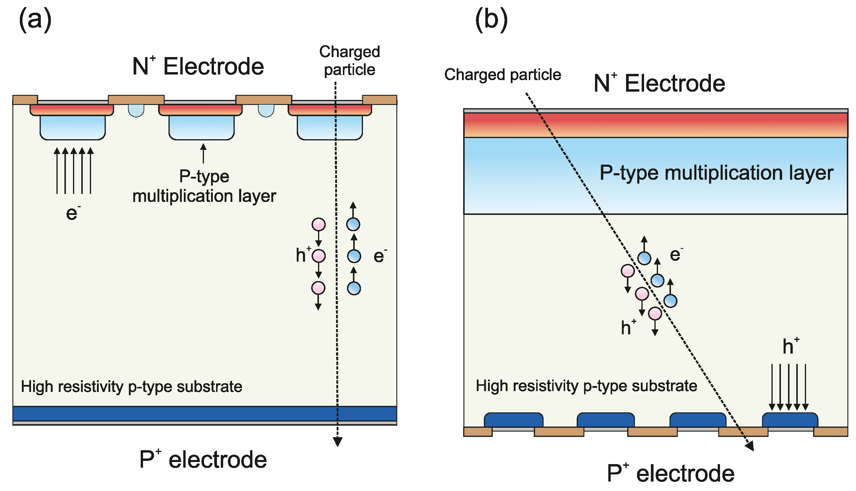
:1. Introduction
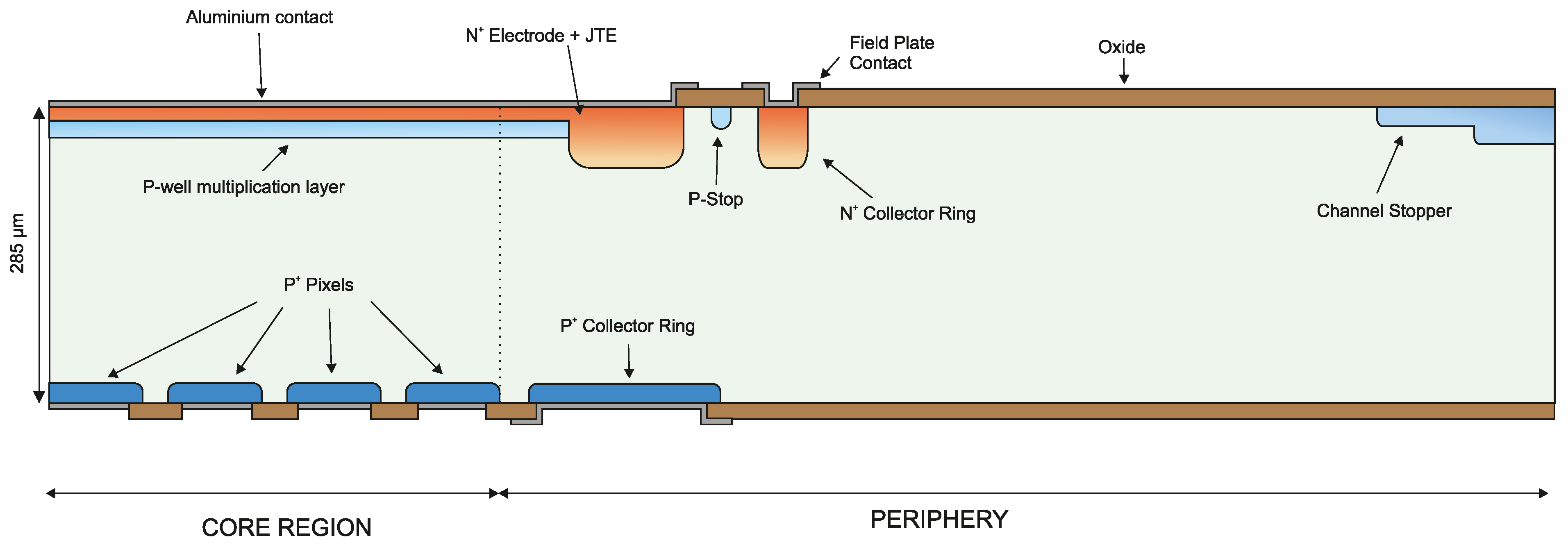
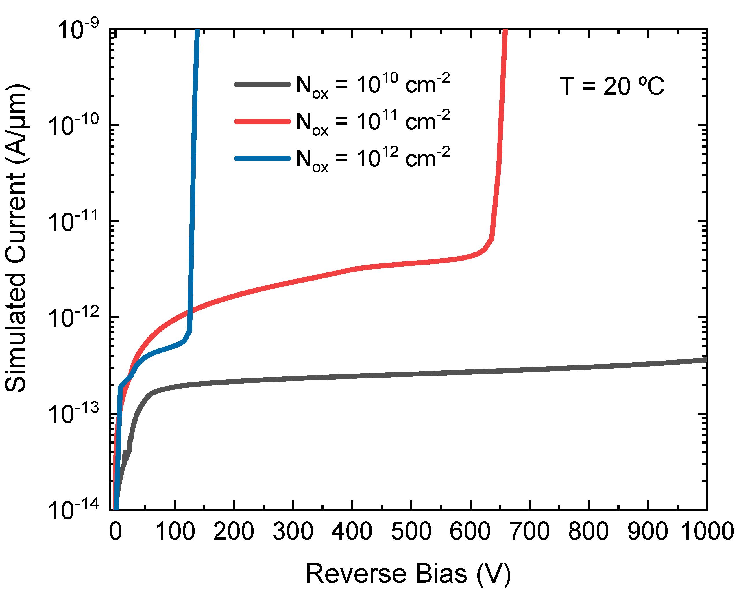
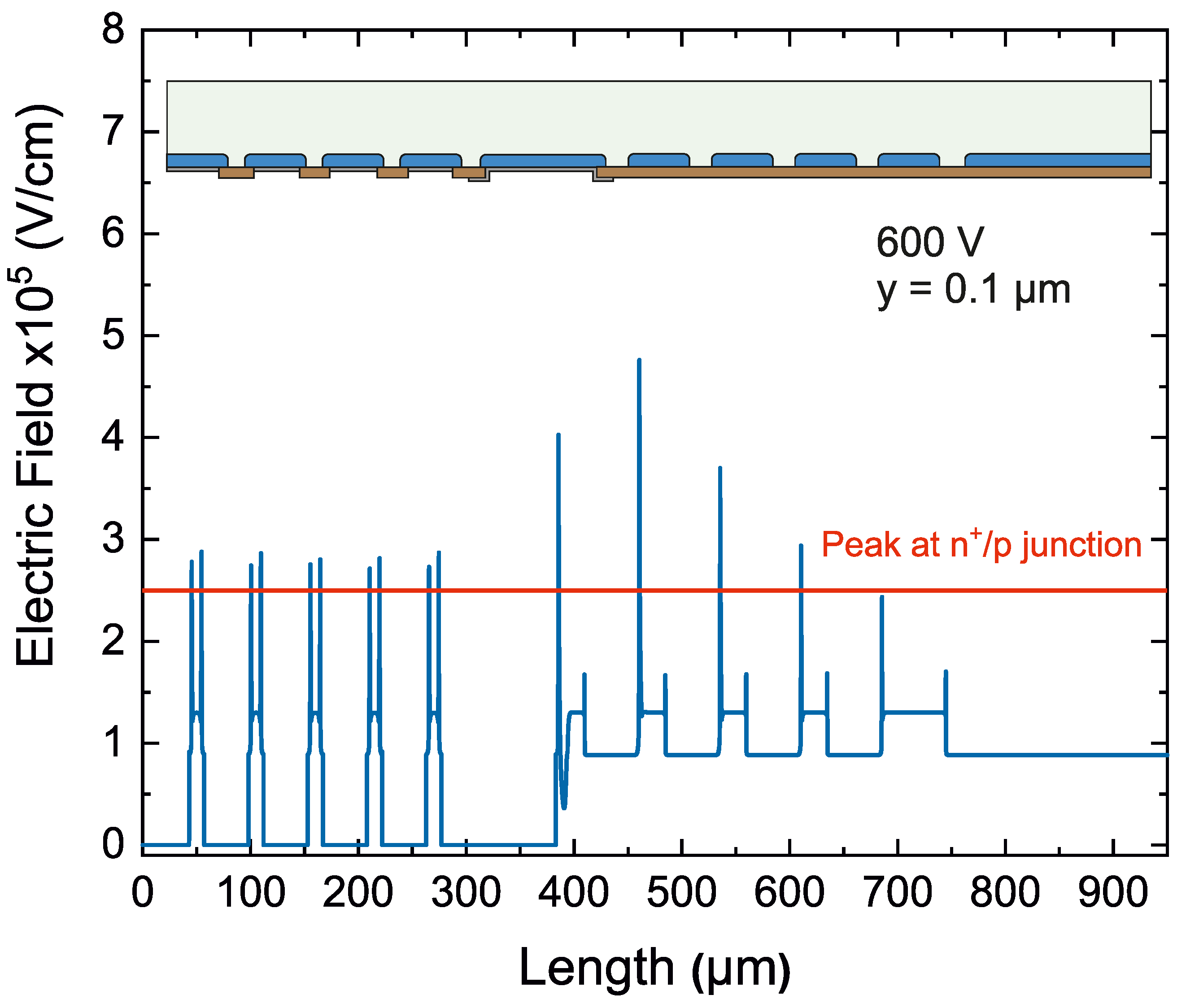
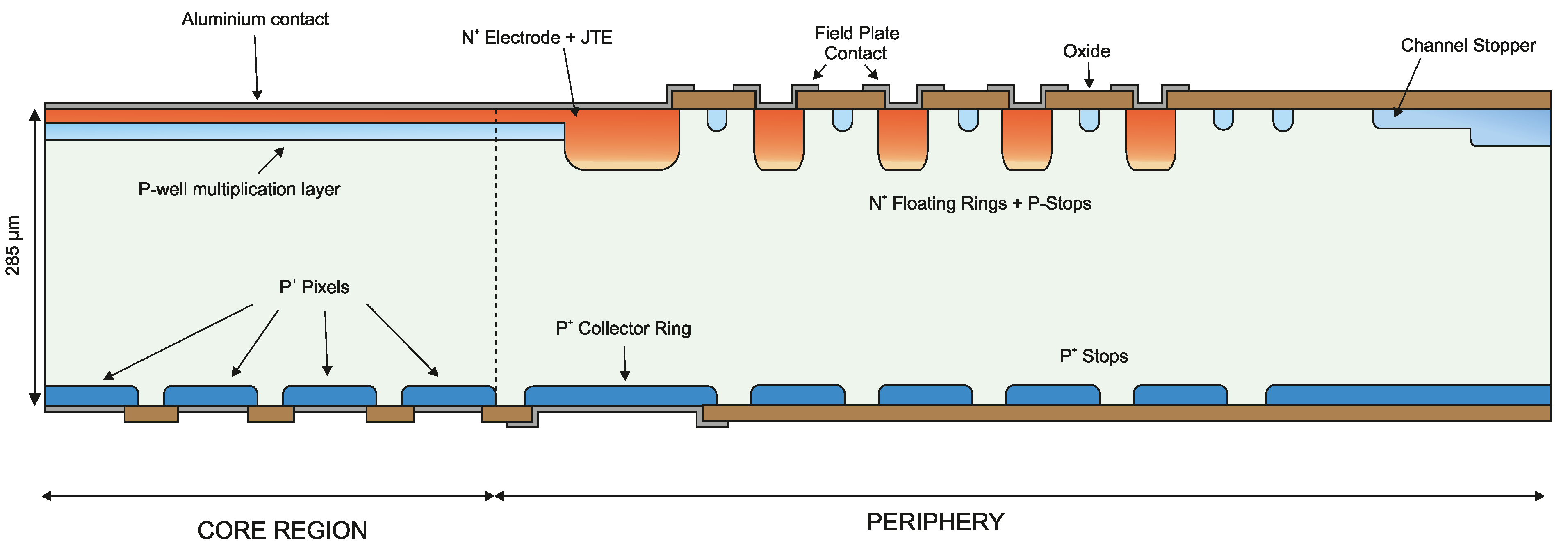
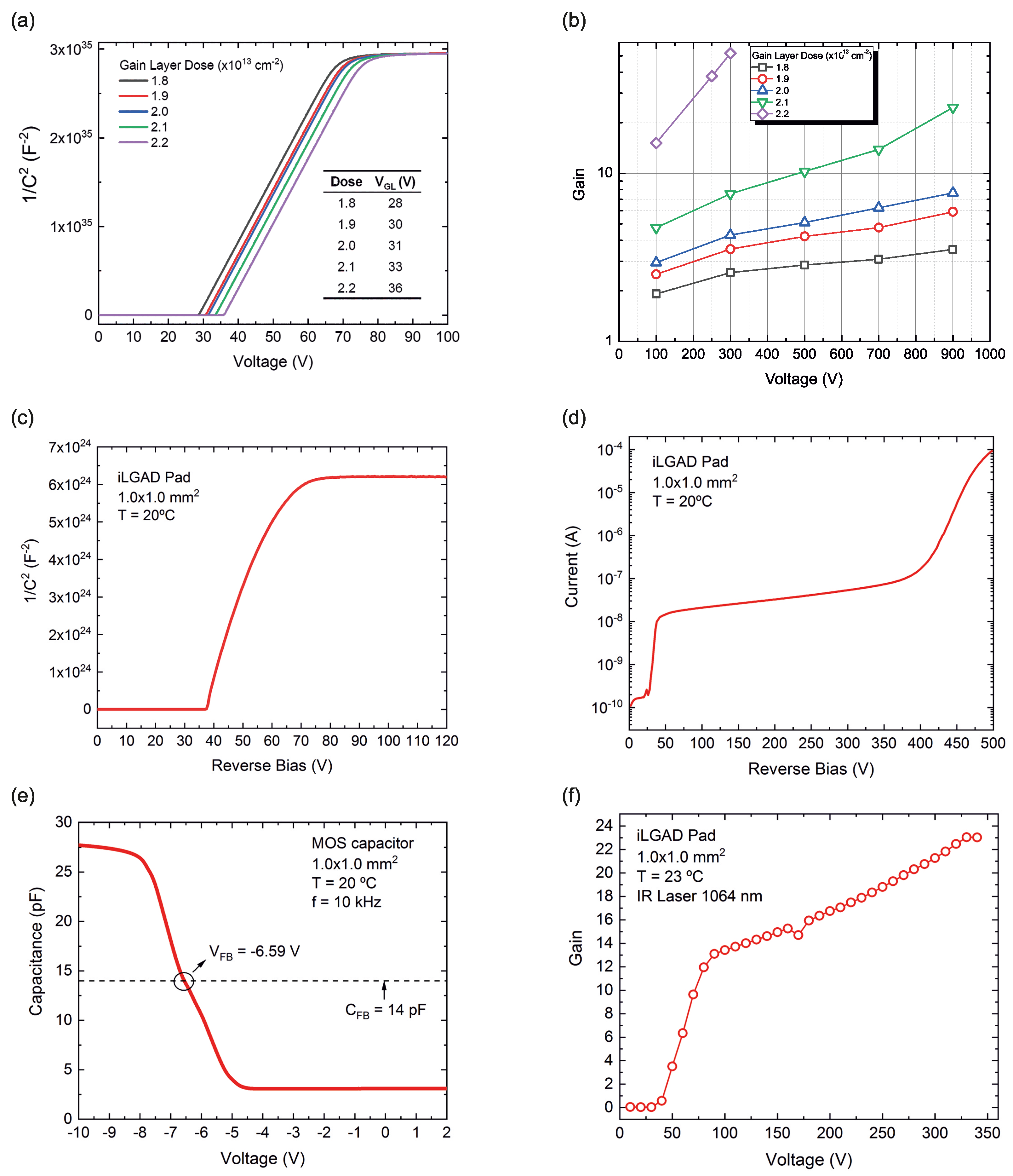
2. Optimization of the iLGAD Periphery
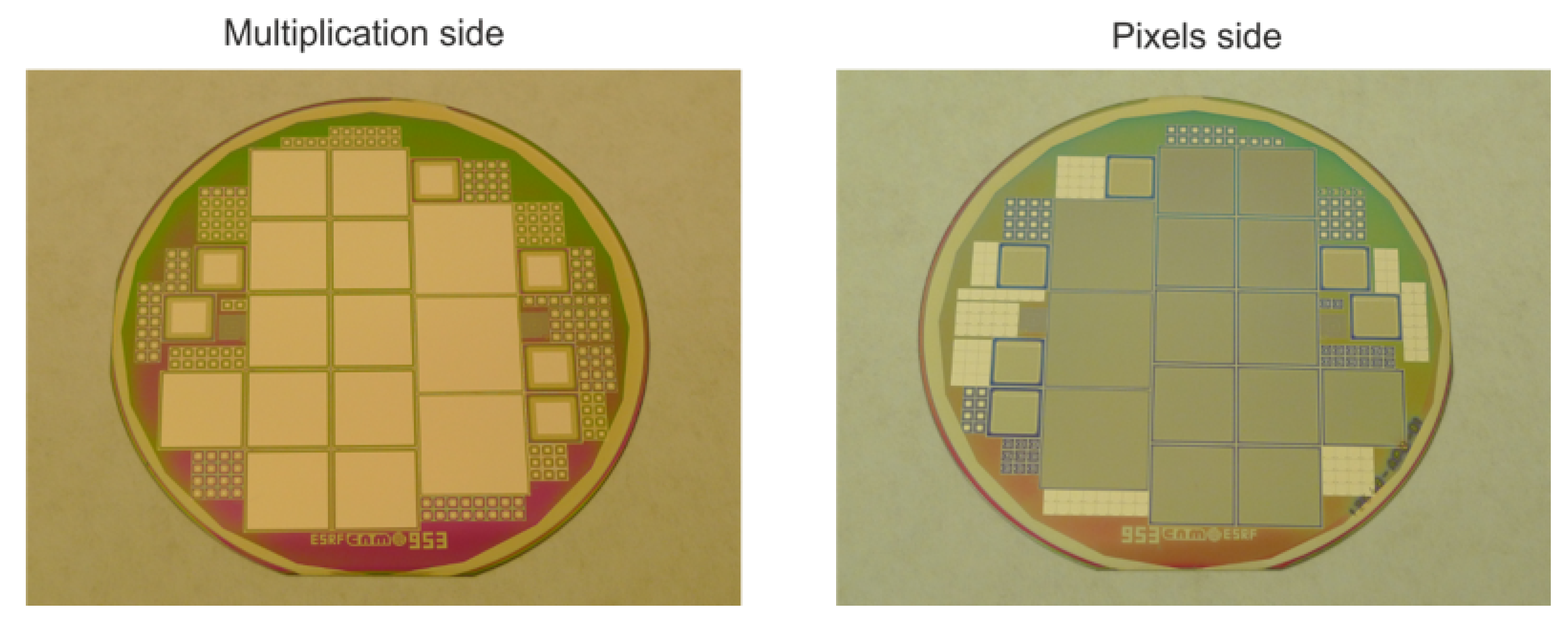
3. Fabrication of the Prototypes
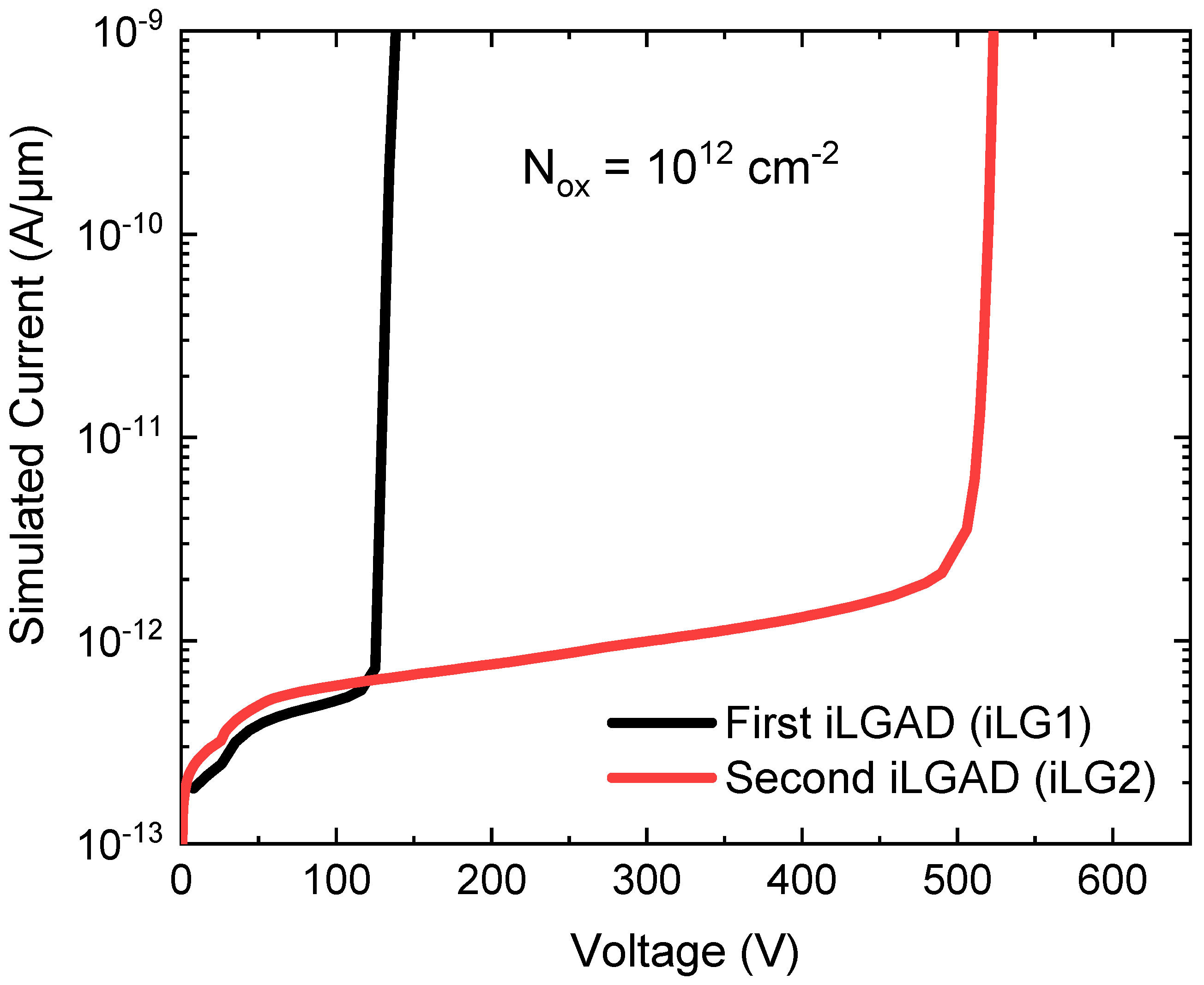
4. Electrical Characterization
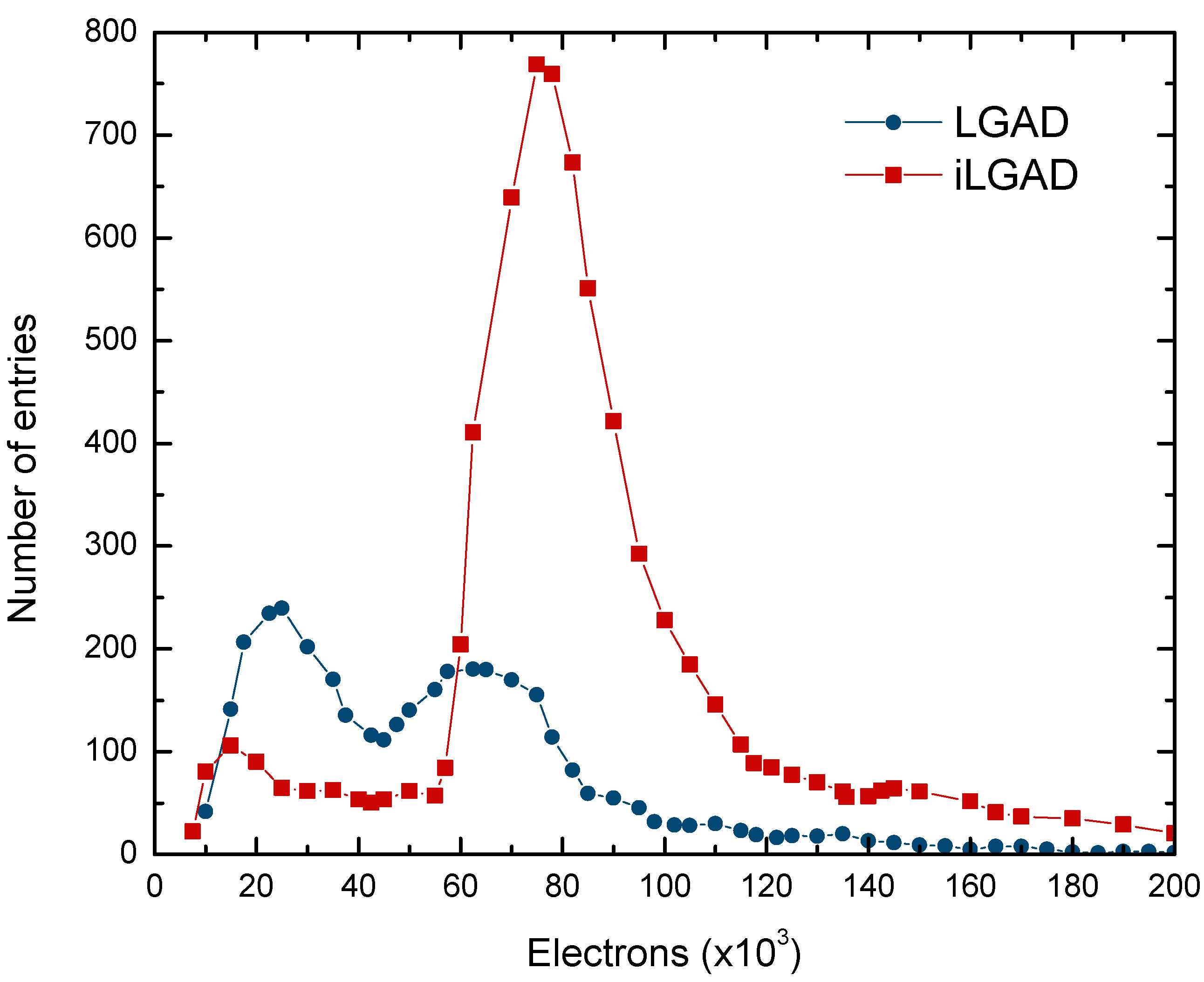
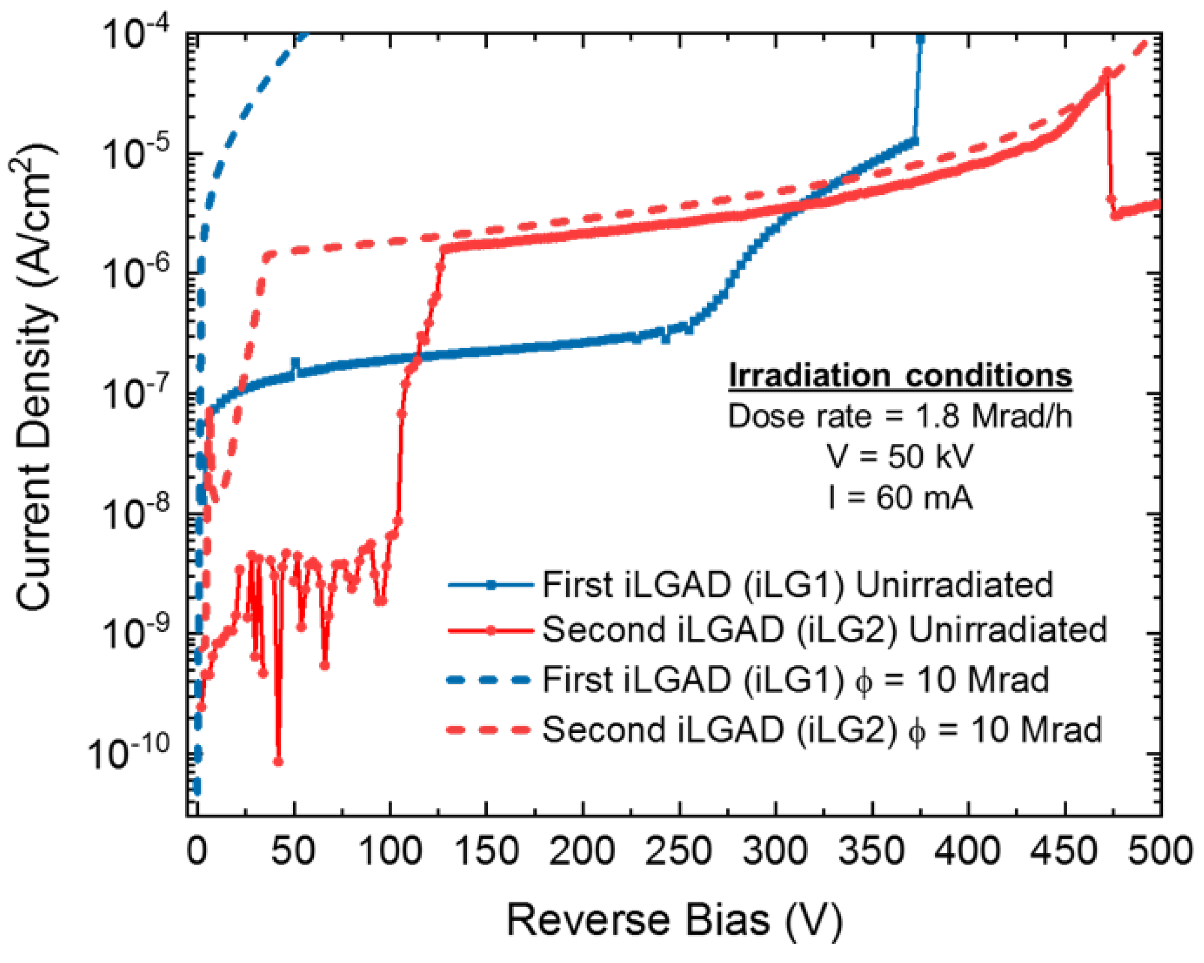
5. Irradiated Samples
6. Conclusions
Author Contributions
Funding
Institutional Review Board Statement
Informed Consent Statement
Data Availability Statement
Conflicts of Interest
References
- Pellegrini, G.; Fernández-Martínez, P.; Baselga, M.; Fleta, C.; Flores, D.; Greco, V.; Hidalgo, S.; Mandić, I.; Kramberger, G.; Quirion, D.; et al. Technology developments and first measurements of Low Gain Avalanche Detectors (LGAD) for high energy physics applications. Nucl. Instrum. Methods Phys. Res. Sect. A Accel. Spectrom. Detect. Assoc. Equip. 2014, 765, 12–16. [Google Scholar] [CrossRef]
- Carulla, M.; Doblas, A.; Flores, D.; Galloway, Z.; Hidalgo, S.; Kramberger, G.; Luce, Z.; Mandić, I.; Mazza, S.; Merlos, A.; et al. 50 µm thin Low Gain Avalanche Detectors (LGAD) for timing applications. Nucl. Instrum. Methods Phys. Res. Sect. A Accel. Spectrom. Detect. Assoc. Equip. 2019, 924, 373–379. [Google Scholar] [CrossRef]
- Sadrozinski, H.F.; Seiden, A.; Cartiglia, N. 4D tracking with ultra-fast silicon detectors. Rep. Progress Phys. 2017, 81, 026101. [Google Scholar] [CrossRef] [PubMed]
- Moffat, N.; Bates, R.; Bullough, M.; Flores, L.; Maneuski, D.; Simon, L.; Tartoni, N.; Doherty, F. Low Gain Avalanche Detectors (LGAD) for particle physics and synchrotron applications. J. Instrum. 2018, 13, C03014. [Google Scholar] [CrossRef]
- Yang, X.; Alderweireldt, S.; Atanov, N.; Ayoub, M.K.; da Costa, J.B.G.; García, L.C.; Chen, H.; Christie, S.; Cindro, V.; Cui, H.; et al. Layout and performance of HPK prototype LGAD sensors for the High-Granularity Timing Detector. Nucl. Instrum. Methods Phys. Res. Sect. A Accel. Spectrom. Detect. Assoc. Equip. 2020, 980, 164379. [Google Scholar] [CrossRef]
- Pellegrini, G.; Baselga, M.; Carulla, M.; Fadeyev, V.; Fernández-Martínez, P.; García, M.F.; Flores, D.; Galloway, Z.; Gallrapp, C.; Hidalgo, S.; et al. Recent technological developments on LGAD and iLGAD detectors for tracking and timing applications. Nucl. Instrum. Methods Phys. Res. Sect. A Accel. Spectrom. Detect. Assoc. Equip. 2016, 931, 24–28. [Google Scholar] [CrossRef] [Green Version]
- Carulla, M.; Fernandez-Garcia, M.; Fernandez-Martinez, P.; Flores, D.; Gonzalez, J.; Hidalgo, S.; Jaramillo, R.; Merlos, A.; Palomo, F.R.; Pellegrini, G.; et al. Technology developments and first measurements on inverse Low Gain Avalanche Detector (iLGAD) for high energy physics applications. J. Instrum. 2016, 11, C12039. [Google Scholar] [CrossRef]
- Currás, E.; Carulla, M.; Vignali, M.C.; Duarte-Campderros, J.; Fernández, M.; Flores, D.; García, A.; Gómez, G.; González, J.; Hidalgo, S.; et al. Inverse Low Gain Avalanche Detectors (iLGADs) for precise tracking and timing applications. Nucl. Instrum. Methods Phys. Res. Sect. A Accel. Spectrom. Detect. Assoc. Equip. 2020, 958, 162545. [Google Scholar] [CrossRef] [Green Version]
- Vila, I. An in-depth study of Inverse-LGAD sensors. In Proceedings of the 13th Trento Workshop on Advanced Silicon Radiation Detectors, Munich, Germany, 19–20 February 2018. [Google Scholar]
- Duarte-Campderros, J. Inverse-LGAD: Solving the LGAD fill factor problem. In Proceedings of the 31st RD50 Workshop, Geneva, Switzerland, 20–22 November 2017. [Google Scholar]
- Lange, J.; Carulla, M.; Cavallaro, E.; Chytka, L.; Davis, P.M.; Flores, D.; Förster, F.; Grinstein, S.; Hidalgo, S.; Komarek, T.; et al. Gain and time resolution of 45 µm thin Low Gain Avalanche Detectors before and after irradiation up to a fluence of 1015 neq/cm2. J. Instrum. 2017, 12, P05003. [Google Scholar] [CrossRef] [Green Version]
- Swinehart, D.F. The beer-lambert law. J. Chem. Educ. 1962, 39, 333. [Google Scholar] [CrossRef]
- Takahashi, T.; Watanabe, S. Recent progress in CdTe and CdZnTe detectors. IEEE Trans. Nucl. Sci. 2001, 48, 950959. [Google Scholar] [CrossRef] [Green Version]
- Lioliou, G.; Whitaker, M.D.C.; Barnett, A.M. High temperature GaAs X-ray detectors. J. Appl. Phys. 2017, 122, 244506. [Google Scholar] [CrossRef] [Green Version]
- Schwandt, J. Design of a Radiation Hard Silicon Pixel Sensor for Xray Science (No. DESY-THESIS–2014-029). Ph.D. Thesis, Hamburg University, Hamburg, Germany, 2014. [Google Scholar]
- Medipix3 Website. Available online: https://medipix.web.cern.ch/medipix3 (accessed on 20 November 2022).
- Mozzanica, A.; Andrä, M.; Barten, R.; Bergamaschi, A.; Chiriotti, S.; Brückner, M.; Dinapoli, R.; Fröjdh, E.; Greiffenberg, D.; Leonarski, F.; et al. The JUNGFRAU detector for applications at synchrotron light sources and XFELs. Synchrotron Radiat. News 2018, 31, 16–20. [Google Scholar] [CrossRef]
- Knoll, G.F. Radiation Detection and Measurement; John Wiley & Sons: Hoboken, NJ, USA, 2010. [Google Scholar]
- Eremin, V.; Strokan, N.; Verbitskaya, E.; Li, Z. Development of transient current and charge techniques for the measurement of effective net concentration of ionized charges (Neff) in the space charge region of pn junction detectors. Nucl. Instrum. Methods Phys. Res. Sect. A Accel. Spectrom. Detect. Assoc. Equip. 1996, 372, 388–398. [Google Scholar] [CrossRef]


Disclaimer/Publisher’s Note: The statements, opinions and data contained in all publications are solely those of the individual author(s) and contributor(s) and not of MDPI and/or the editor(s). MDPI and/or the editor(s) disclaim responsibility for any injury to people or property resulting from any ideas, methods, instructions or products referred to in the content. |
© 2023 by the authors. Licensee MDPI, Basel, Switzerland. This article is an open access article distributed under the terms and conditions of the Creative Commons Attribution (CC BY) license (https://creativecommons.org/licenses/by/4.0/).
Share and Cite
Doblas, A.; Flores, D.; Hidalgo, S.; Moffat, N.; Pellegrini, G.; Quirion, D.; Villegas, J.; Maneuski, D.; Ruat, M.; Fajardo, P. Inverse LGAD (iLGAD) Periphery Optimization for Surface Damage Irradiation. Sensors 2023, 23, 3450. https://doi.org/10.3390/s23073450
Doblas A, Flores D, Hidalgo S, Moffat N, Pellegrini G, Quirion D, Villegas J, Maneuski D, Ruat M, Fajardo P. Inverse LGAD (iLGAD) Periphery Optimization for Surface Damage Irradiation. Sensors. 2023; 23(7):3450. https://doi.org/10.3390/s23073450
Chicago/Turabian StyleDoblas, Albert, David Flores, Salvador Hidalgo, Neil Moffat, Giulio Pellegrini, David Quirion, Jairo Villegas, Dzmitry Maneuski, Marie Ruat, and Pablo Fajardo. 2023. "Inverse LGAD (iLGAD) Periphery Optimization for Surface Damage Irradiation" Sensors 23, no. 7: 3450. https://doi.org/10.3390/s23073450