
A 21.4 pW Subthreshold Voltage Reference with 0.020 %/V Line Sensitivity Using DIBL Compensation

1
Department of Information Technology and Electrical Engineering, ETH Zurich, 8092 Zurich, Switzerland
2
Department of Electronic Engineering, Hanbat National University, Daejeon 34158, Republic of Korea
*
Author to whom correspondence should be addressed.
Sensors 2023, 23(4), 1862; https://doi.org/10.3390/s23041862
Submission received: 30 December 2022
/
Revised: 31 January 2023
/
Accepted: 3 February 2023
/
Published: 7 February 2023
(This article belongs to the Special Issue Integrated Circuits and CMOS Sensors)
Abstract
:This paper presents an ultra-low-power voltage reference designed in 180 nm CMOS technology. To achieve near-zero line sensitivity, a two-transistor (2-T) voltage reference is biased with a current source to cancel the drain-induced barrier-lowering (DIBL) effect of the 2-T core, thus improving the line sensitivity. This compensation circuit achieves a Monte-Carlo-simulated line sensitivity of 0.035 %/V in a supply range of 0.6 to 1.8 V, while generating a reference voltage of 307.8 mV, with 21.4 pW power consumption. The simulated power supply rejection ratio (PSRR) is −54 dB at 100 Hz. It also achieves a temperature coefficient of 24.8 ppm/°C in a temperature range of −20 to 80 °C, with a projected area of 0.003 mm2.
1. Introduction
With the growing demand for energy-efficient and portable devices, such as IoT sensors or biomedical applications, power and area constraints on integrated circuits (ICs) are becoming increasingly more significant due to the limited energy source and the system volume.
A voltage reference is a key building block for analog and mixed-signal ICs. It generates a well-defined and stable voltage, irrespective of variations in the supply voltage and temperature. A bandgap reference (BGR) is commonly adopted for such applications, thanks to its superior temperature coefficient (TC) and line sensitivity (LS), which indicate how the reference voltage varies depending on the temperature and supply voltage, respectively. Such BGRs are implemented with a proportional-to-absolute-temperature (PTAT) voltage that cancels the TC of a complementary-to-absolute-temperature (CTAT) voltage of a BJT [1,2,3]. For ultra-low-power miniaturized systems, however, the area, power consumption and supply requirements make it difficult to employ a BGR as a voltage reference. A viable alternative featuring a low supply voltage, pW-level power consumption and small area is a subthreshold voltage reference [4,5,6,7,8,9,10,11,12,13,14]. The two-transistor (2-T) reference in [4] achieves a fine LS of 0.044 %/V and a low TC of 54~176 ppm/°C, while consuming 5.5 pW and occupying a 1425 µm2 area. However, further improvement in the LS is limited due to the drain-to-source voltage dependency of the pull-up transistor implemented with the native transistor due to the drain-induced barrier-lowering (DIBL) effect. To improve the LS, [5] applies a self-regulating circuit to the 2-T reference and achieves a better LS of 0.0154 %/V. A self-biased voltage reference based on a self-cascoded MOSFET (SCM) is proposed in [6], improving the LS and TC at the cost of higher power consumption. Another self-biased voltage reference presented in [7] aims to make the biasing current supply independent, offering further LS improvements. However, the self-regulating circuit consumes much more power than the 2-T core (e.g., 1 nW in [5]), causing a significant power penalty. Furthermore, the self-biasing circuits require additional start-up circuits due to multiple operating points, increasing the circuit complexity and area requirement.
This paper proposes an ultra-low-power CMOS voltage reference that consumes 21.4 pW, with an enhanced compensation to achieve a LS of 0.020 %/V without using complex and power-hungry start-up and self-biasing circuits.
The remainder of this paper is structured as follows. Section 2 introduces the DIBL effect of the transistors in the proposed design and its impact on the LS. Section 3 describes the design and implementation of the proposed voltage reference. Section 4 briefly summarizes the design methodology. Section 5 presents the simulation results, and Section 6 concludes the paper.
2. DIBL Effect
DIBL is one of the prominent non-idealities in short-channel MOSFET devices and refers to the dependency of a MOSFET’s drain current on its drain-source voltage, . This effect can be modeled as a reduction of the transistor’s threshold voltage, , as a function of [15]:
where is the threshold voltage as approaches zero, and is the DIBL effect factor. As the channel length decreases, typically increases.
The subthreshold current of a MOSFET is given by:
where and , and , , and are the carrier mobility, oxide capacitance, subthreshold slope factor and thermal voltage, respectively. Typically, the last term of (2), , becomes negligible when is sufficiently higher than (e.g., ).
Therefore, by combining (1) and (2) while eliminating the last term of (2), we can obtain:
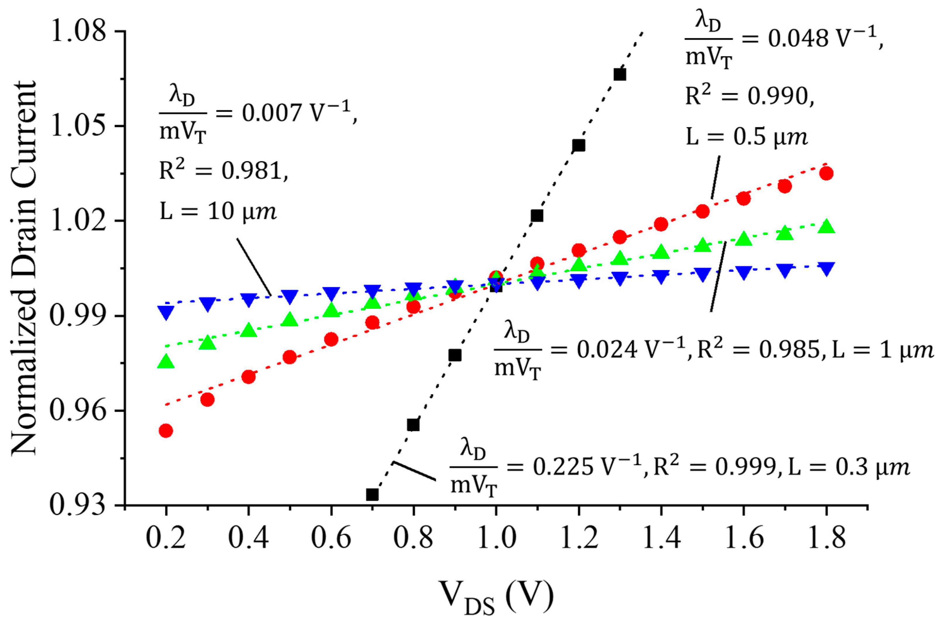
This clearly demonstrates the drain-source current’s dependence on for a large , i.e., shorter channel lengths. Figure 1 shows the simulated drain current of a 3V PMOS device affected by the DIBL effect in a 180 nm CMOS technology. For , the drain current can be approximated as a linear function of with a reasonable error less than 2 % (worst case), as indicated in [7]. This work models such a linear DIBL current using an effective aspect ratio , similarly to [7]:
where is the of the MOSFET, and is the slope factor of the DIBL effect on the drain current, i.e., the slope of as a function of .
3. Design and Analysis
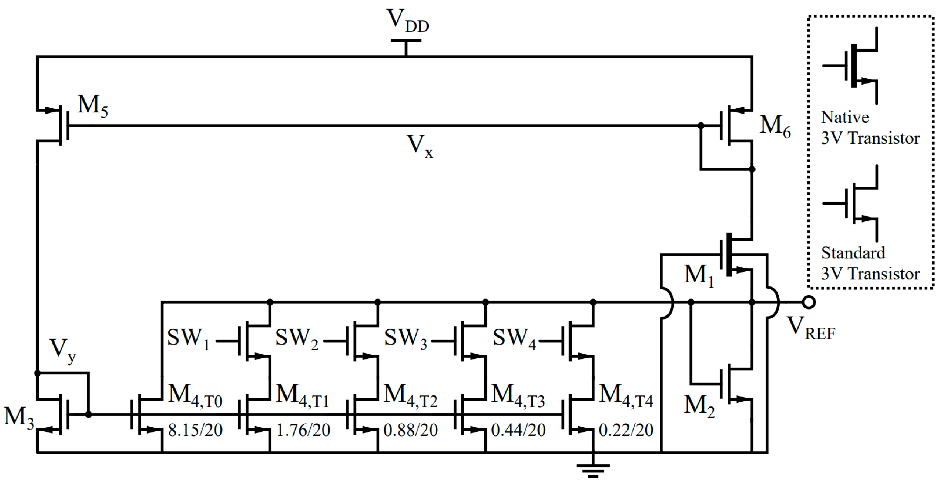
3.1. Circuit Description
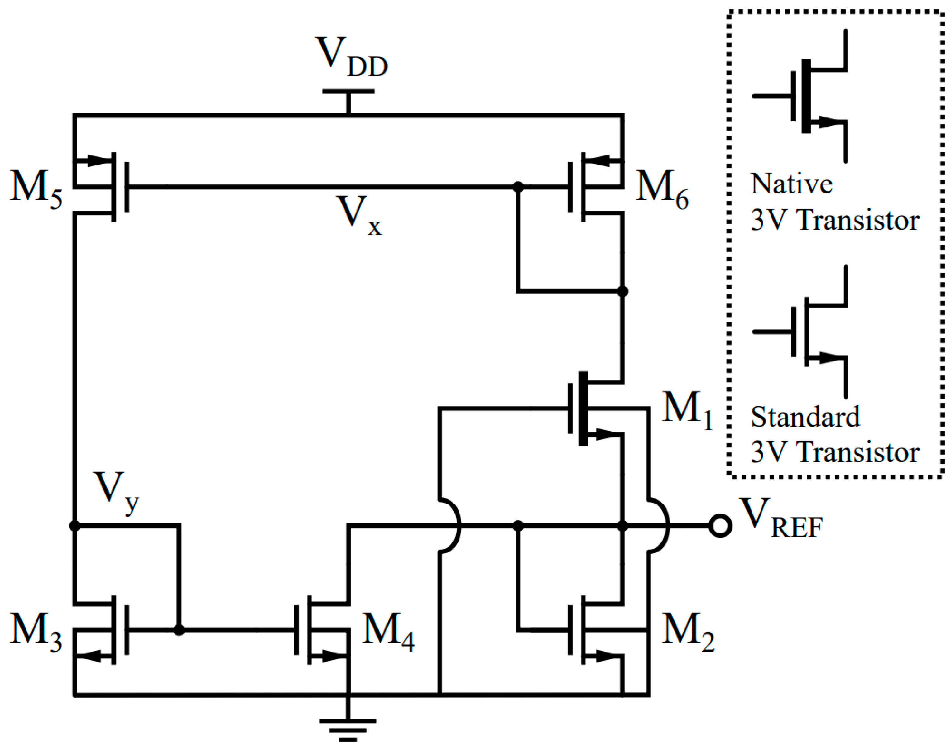
A schematic of the proposed voltage reference is shown in Figure 2, and its sizing dimensions are listed in Table 1. It employs the 2-T voltage reference proposed in [4], formed by a native NMOS transistor (M1) stacked on top of a standard NMOS transistor (M2), generating a reference voltage defined as a function of . The native transistor has a low or near-zero , which is much smaller than that of the standard transistor. To improve the supply independency, it performs compensation for the DIBL effect [7]. M5 and M6 generate currents dependent on the drain voltage due to the DIBL effect, which causes these currents to depend not only on the gate-source voltages of M5 and M6, but also on their drain-source voltages . Due to the low resistance of the diode-configured transistor, M6, is almost constant along the supply change, whereas directly follows the supply change.
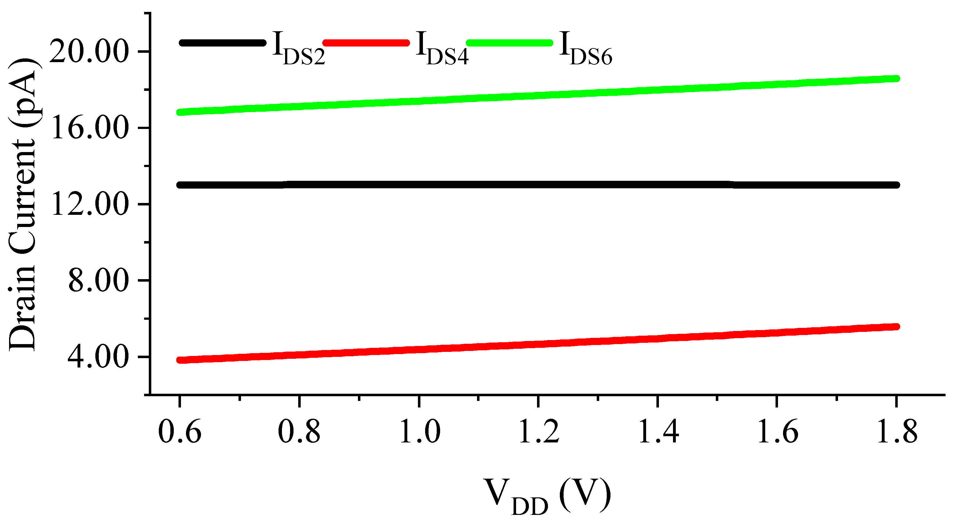
Therefore, the current generated by M5 has a stronger supply dependency than the current generated by M6. The current mirror formed by M3 and M4 copies the current generated by M5 and subtracts it from the current generated by M1. Thus, the appropriate widths of M3 and M4 lead to a supply-independent current through M2 (Figure 3), resulting in a supply-independent reference voltage .
It is worth noting that the proposed voltage reference does not need additional branches to generate a biasing current. In addition, the proposed circuit only has one operating point due to the always-on leakage current of M1. Thus, it does not require an additional start-up circuit, either. The current through M1 and M6 is determined by the width and length of M1. Then, the current is mirrored to M5 and flows into M3. This current is again mirrored to M4, so the impedance of the diode-configured MOS transistors (M6 and M3) defines VX and VY. The current of M2 becomes and M2 converts the current to the reference voltage.
3.2. Minimum Supply Voltage
As mentioned above, (3) is only true for a large (e.g., ). Hence, the minimum supply voltage of the proposed circuit is decided by the output voltage, , plus two drain-source voltages, resulting in:
The low minimum-supply voltage is suitable for most low-power applications and contrasts with that of a BGR architecture, which is at least ~1.4 V ().
3.3. Temperature Coefficient
The proposed circuit operates robustly against temperature changes, as its 2-T structure, composed of M1 and M2, generates the output voltage as a function of the threshold voltage difference. Still, due to the additional current of the LS compensation circuit, the optimal transistor dimensions in the 2-T core for the lowest TC are different from the dimensions introduced in [4]. Assuming M5 and M6 are identical transistors, i.e., and , we have , and , where represents of . To account for the influence of the DIBL effect, and are modeled as effective aspect ratios, as described in (4), which entails . Applying Kirchhoff’s current law at the output voltage, the current flowing into M2 can be written as:
and can be re-written by using Equation (2), and becomes after passing through the two current mirrors. By arranging Equation (6), can be obtained as:
Finally, assuming and setting the derivative over temperature equal to zero, the optimal transistor size ratio that cancels the temperature dependency of and of the 2-T reference can be obtained as:
where is Boltzmann’s constant, and and are the first-order TCs of and respectively.
3.4. Line Sensitivity
The proposed circuit improves the LS by providing a constant biasing current through M2, which is independent of the supply voltage. By using (2), is obtained as:
The currents and are subject to the DIBL effect, which can be found using (4). As shown in Figure 2, and are equal with each other. As in the derivation of (7), M5 and M6 are assumed to be identical transistors, leading to , , , , and . Applying Kirchhoff’s current law at the output node leads to:
By substituting (4) and (9) into (10), can be described as:
Finally, (9) can be re-written as:
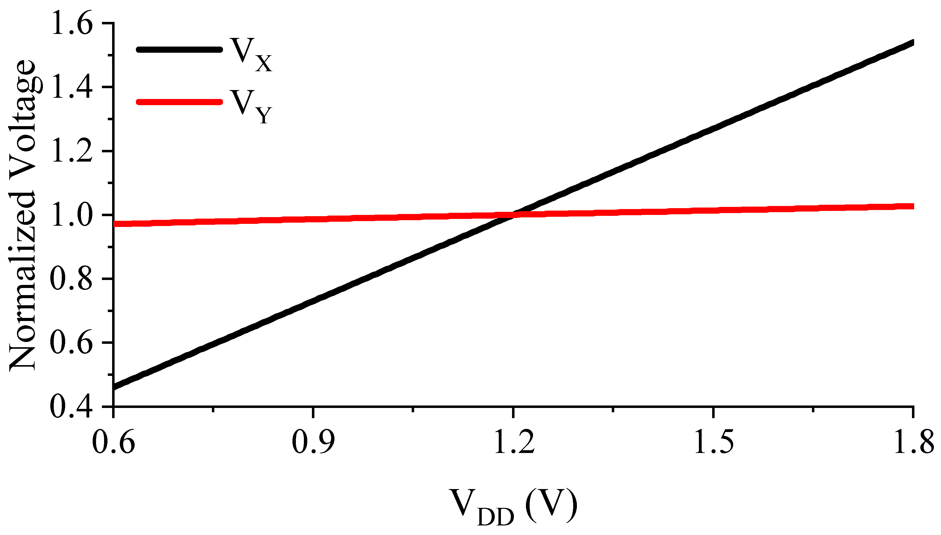
The intermediate node voltages, and (Figure 2), show linear dependencies on the supply voltage, in the given operating supply range of , as shown in the simulation results in Figure 4. This effect also influences and , which can be modeled as follows:
where and are the intermediate voltages and at the minimum operating supply voltage , and and are the slope factors of and , respectively. Combining (12) and (13) results in:
By making Equation equal to zero, the theoretical value for can be derived as:
Equation can be simplified by using:
and the simplified can be derived as:
where and represent the transconductance and output resistance, respectively.
From the initial design point in Equation , the final optimum value can be found after several iterations. As in Equation (7), a change in the ratio leads to a small change in , which in turn affects and, thus, also . Due to the DIBL effect of M6 and the fact that , this then alters both biasing currents, requiring a re-adjustment of . As shown in Figure 5, there is a single optimum point at which to achieve the minimum LS, which is only dependent on the DIBL coefficient of M5. After starting with the initial value of , the next can be decided depending on the sign of . If the sign is negative, it is over-compensated, and needs to be smaller, and vice versa.
3.5. Line Sensitivity
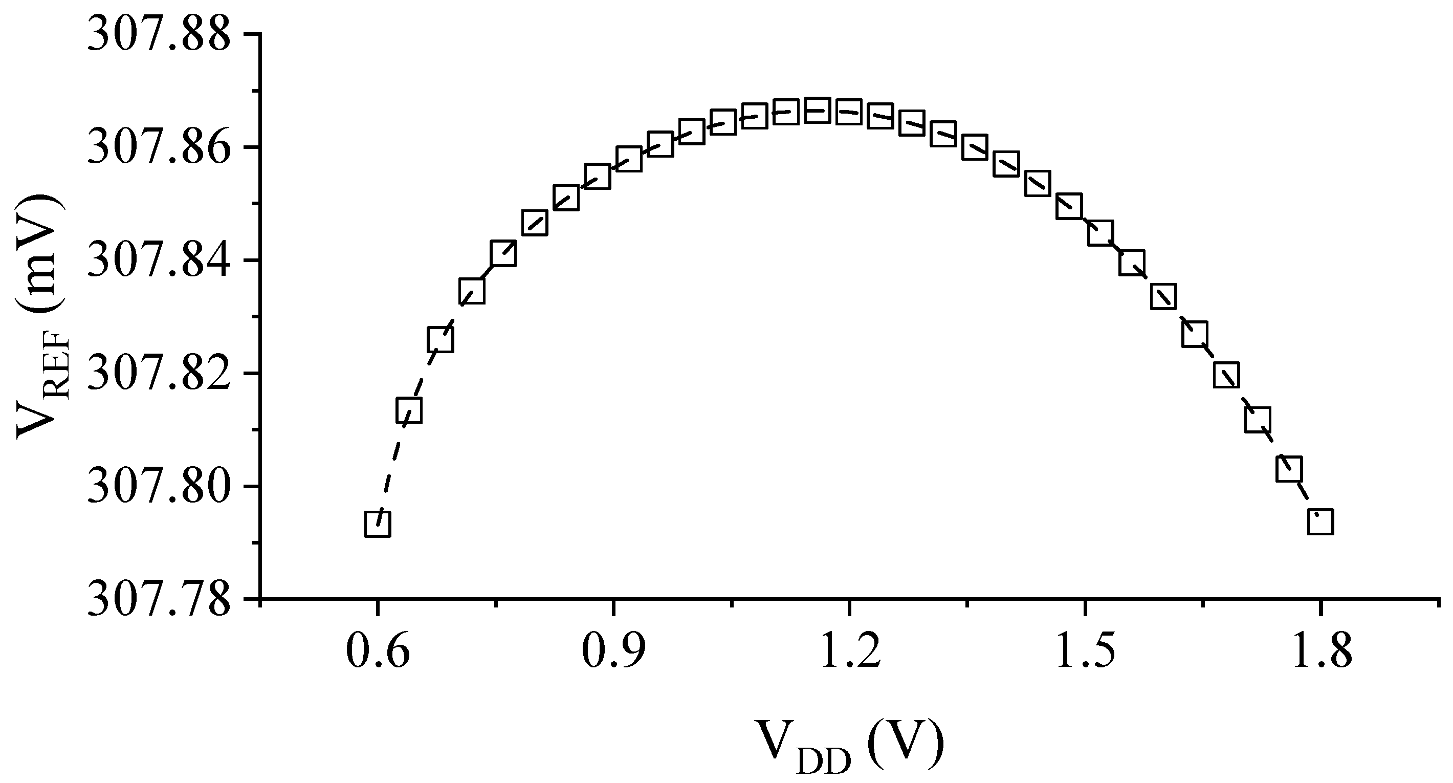
To deal with the impact of possible process and mismatch variations on the LS, the proposed design adopts a trimming block, as shown in Figure 6. The trimming circuit allows the digital adjustment of the bottom current mirror ratio , which will adapt the amount of the compensation current. To cover the most relevant range of possible process variations with sufficient resolution, a 4-bit trimming code is employed to control switches SW1 to SW4, adjusting the mirroring ratio. The default trimming code is 1000, which results in the LS shown in Figure 7 at the nominal condition without any mismatch. After fabrication, the reference voltages at the minimum and maximum supply voltages can be obtained and used to determine the best trimming code by finding the code that minimizes the difference between the voltages. When the reference voltage increases as the supply voltage becomes larger, the trimming code also needs to be increased to make a larger compensating current, and vice versa.
4. Design Methodology
- Determining the dimensions of M5 and M6: The current mirroring ratio between M3 and M4 needs to be small () to reduce the DC bias current of M4, so that the output TC is rarely affected by IDS,4. At the same time, to make the supply-dependent current of M4 match with that of M1 while considering such a small mirroring ratio (Figure 3), the length of the PMOS current mirror (M5) needs to be short to create a relatively large supply-dependent current. The width of M6 is found to set and to achieve .
- Determining the optimal dimensions of the 2-T reference: The temperature sensitivity of the proposed circuit is mainly provided by the 2-T reference. M1 and M2 should, thus, be sized to minimize the TC. This step only considers M1, M2 and M6, i.e., M4 is disconnected from the output node. The length of M1 is chosen to be large enough, such that these transistors mitigate the DIBL effect and obtain a better power supply rejection ratio (PSRR). The width of M1 is set by considering the power budget. Finally, the dimension of M2 is found by using the optimum 2-T ratio found in (8) to minimize the TC of VREF.
- Determining the dimensions of M3 and M4: The channel lengths of M3 and M4 should again be chosen to be large enough for better matching. The proper ratio between M3 and M4 determines the LS of the circuit to cancel the DIBL between M1 and M5, as shown in Figure 3.
- Re-optimizing M2 and M4: The additional current of M4 alters the optimum ratio between M1 and M2 found in (8). It is, thus, suggested to slightly re-adjust the size of M2, which in turn might require another change in M4 to also re-optimize for the lowest LS. This optimization loop can be continued until both the TC and LS settle on satisfactory values.
5. Simulation Results
In this section, we present the SPICE simulation results of the proposed voltage reference scheme shown in Figure 2 and Table 1. To compare the results, the 2-T voltage reference in [4] is also simulated under the same conditions. The dimensions for the transistors in the 2-T core are determined using the values in [4], and the width of the bottom transistor is slightly changed to achieve the minimum TC in the given simulation environment.
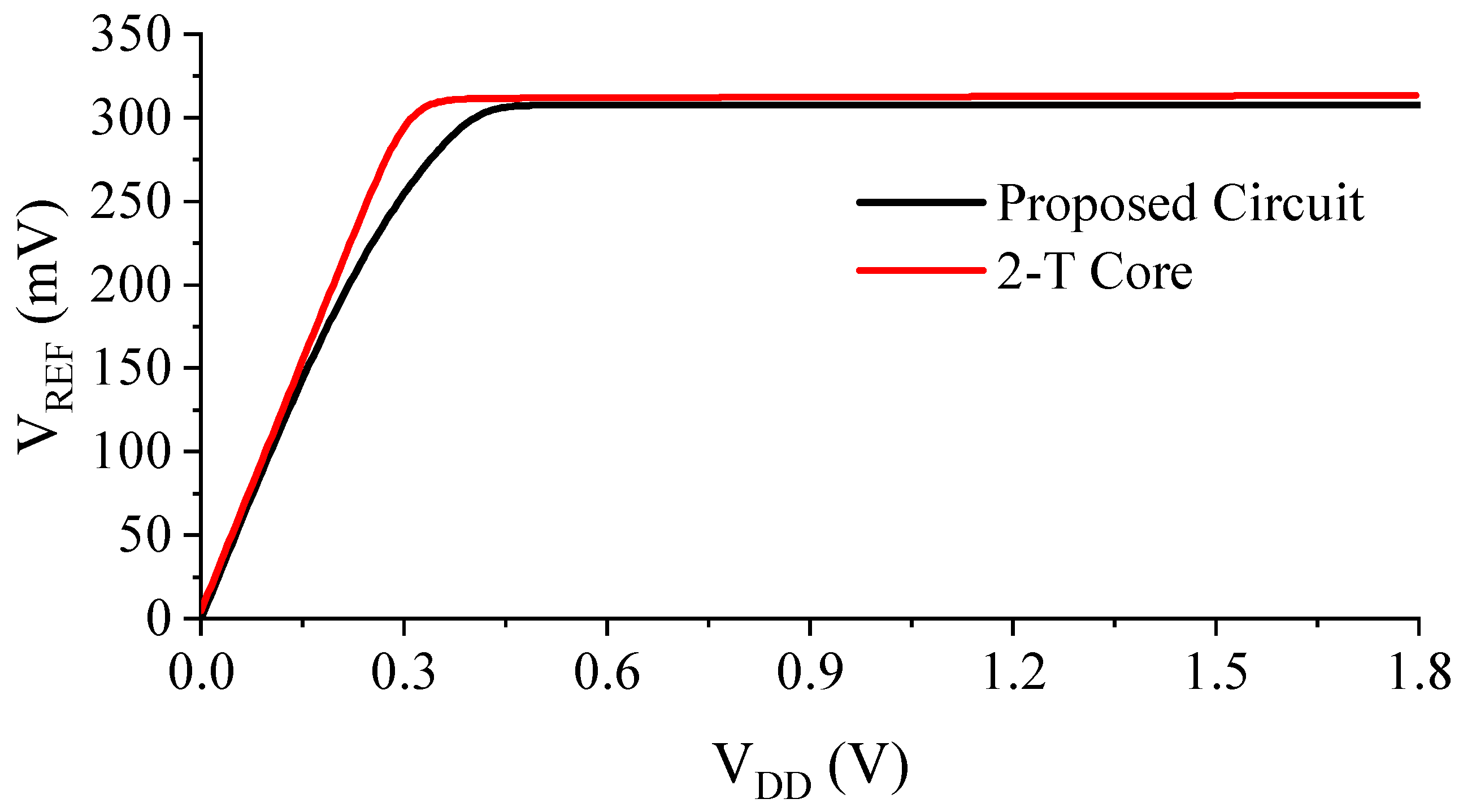
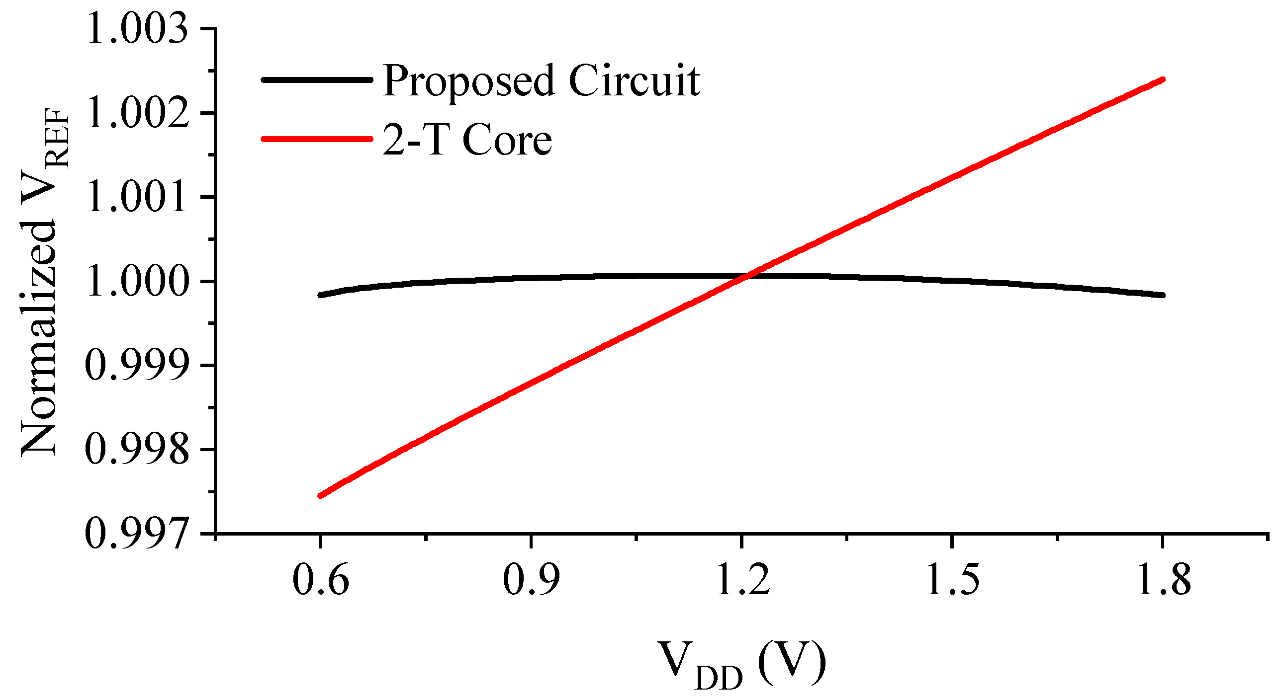
Figure 8 shows the generated reference voltage as a function of the supply voltage in the range of 0–1.8 V. As shown in Figure 7, the proposed design generates a constant of ~307.8 mV with a LS of only 0.020 %/V, which is evaluated using the following equation:
Figure 8 and Figure 9 show the output voltage of the proposed design in comparison with the conventional 2-T reference. Although VDD,min is about 100 mV higher due to the additional M6 connected to the drain of M1, the LS is improved by 18-fold, thanks to the proposed compensation scheme (Figure 9).
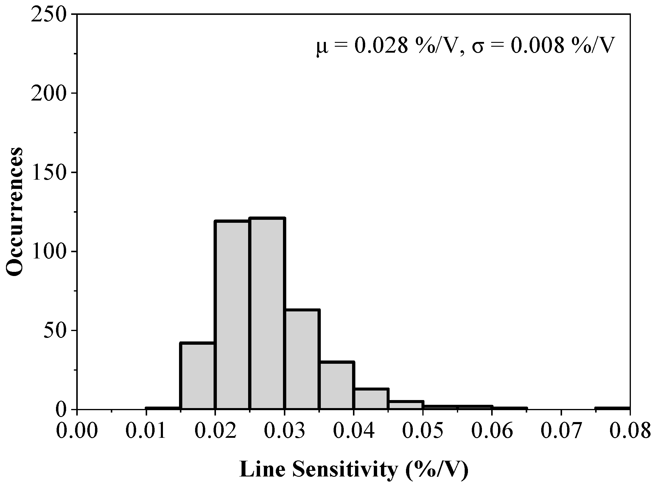
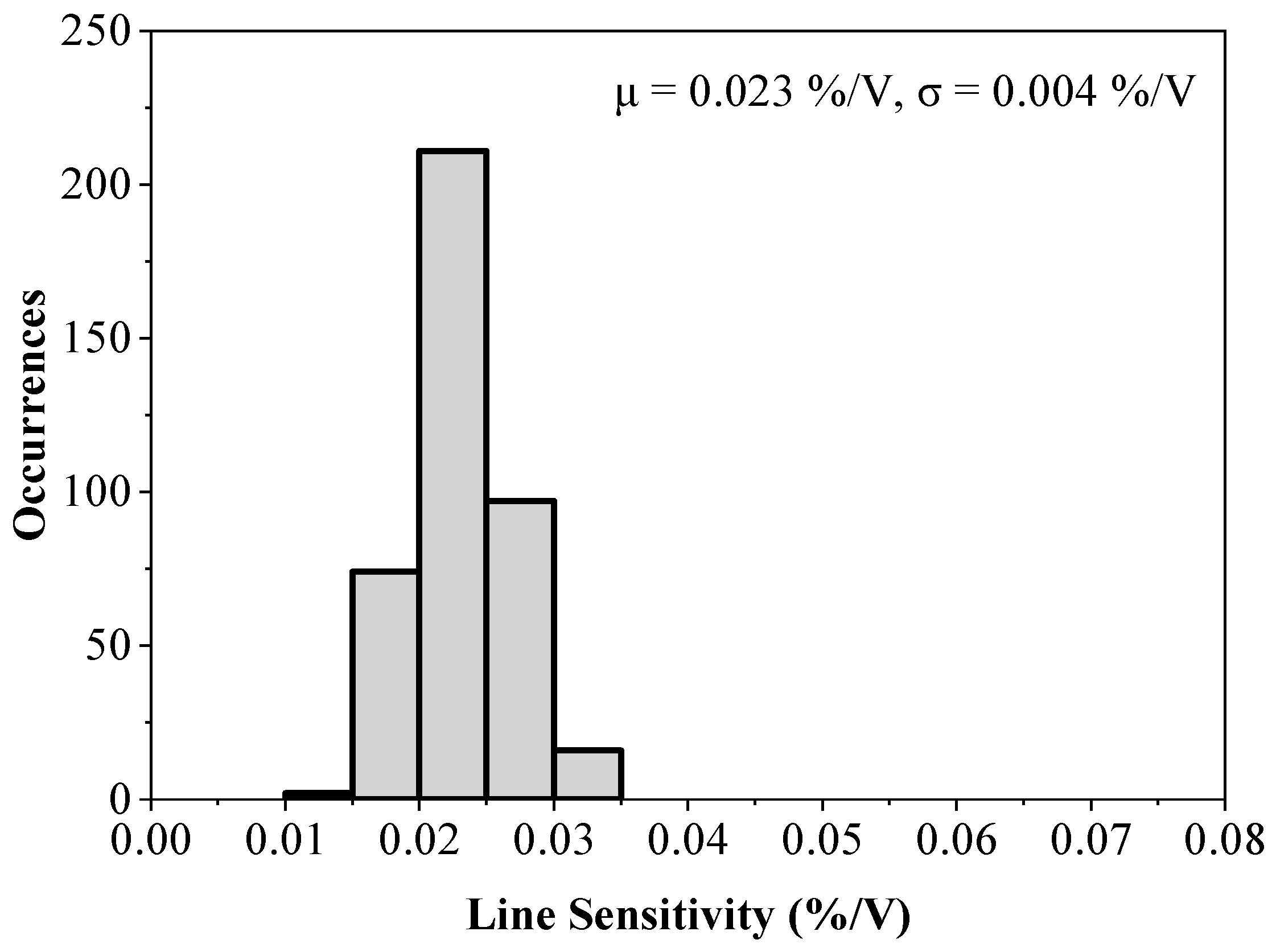
Figure 10 shows the LS of the untrimmed circuit from a 400-point Monte Carlo simulation to verify the performance of the proposed design under the device mismatch. The worst case LS is 0.08 %/V, which is about a 4x increase compared to the case without any variations. Re-running the same Monte Carlo simulation after the 4-bit trimming leads to the results shown in Figure 11. It can be seen that less than 0.035 %/V LS is achieved, validating the superior performance of the proposed voltage reference.
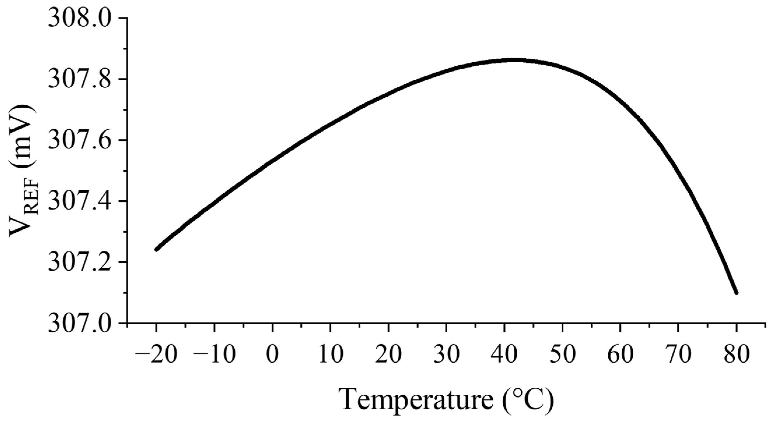
The simulated temperature sensitivity between −20 and 80 °C of the proposed circuit is shown in Figure 12. The TC in ppm/°C is given by the following expression:
In the suggested operating temperature range, a simulated TC of 24.8 ppm/°C is obtained at a supply voltage of 0.6 V.
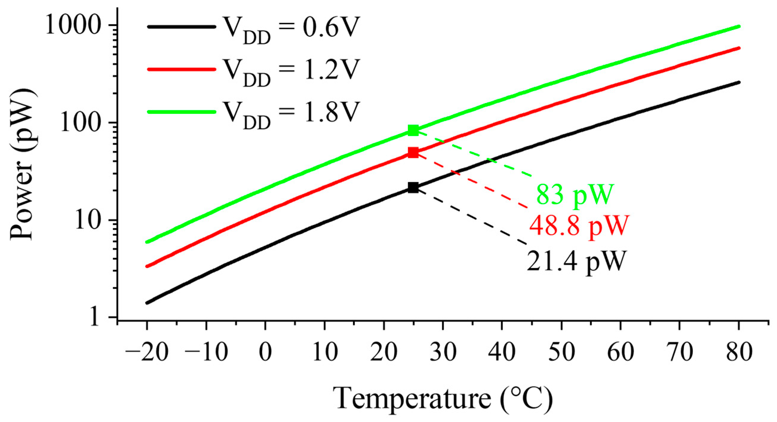
Figure 13 shows the simulated power consumption of the proposed design. At room temperature, the proposed voltage reference requires 21.4 pW at a supply of 0.6 V and 83 pW at the maximum operating supply of 1.8 V. The highest simulated power consumption occurs at and T = 80 °C, reaching 974 pW.
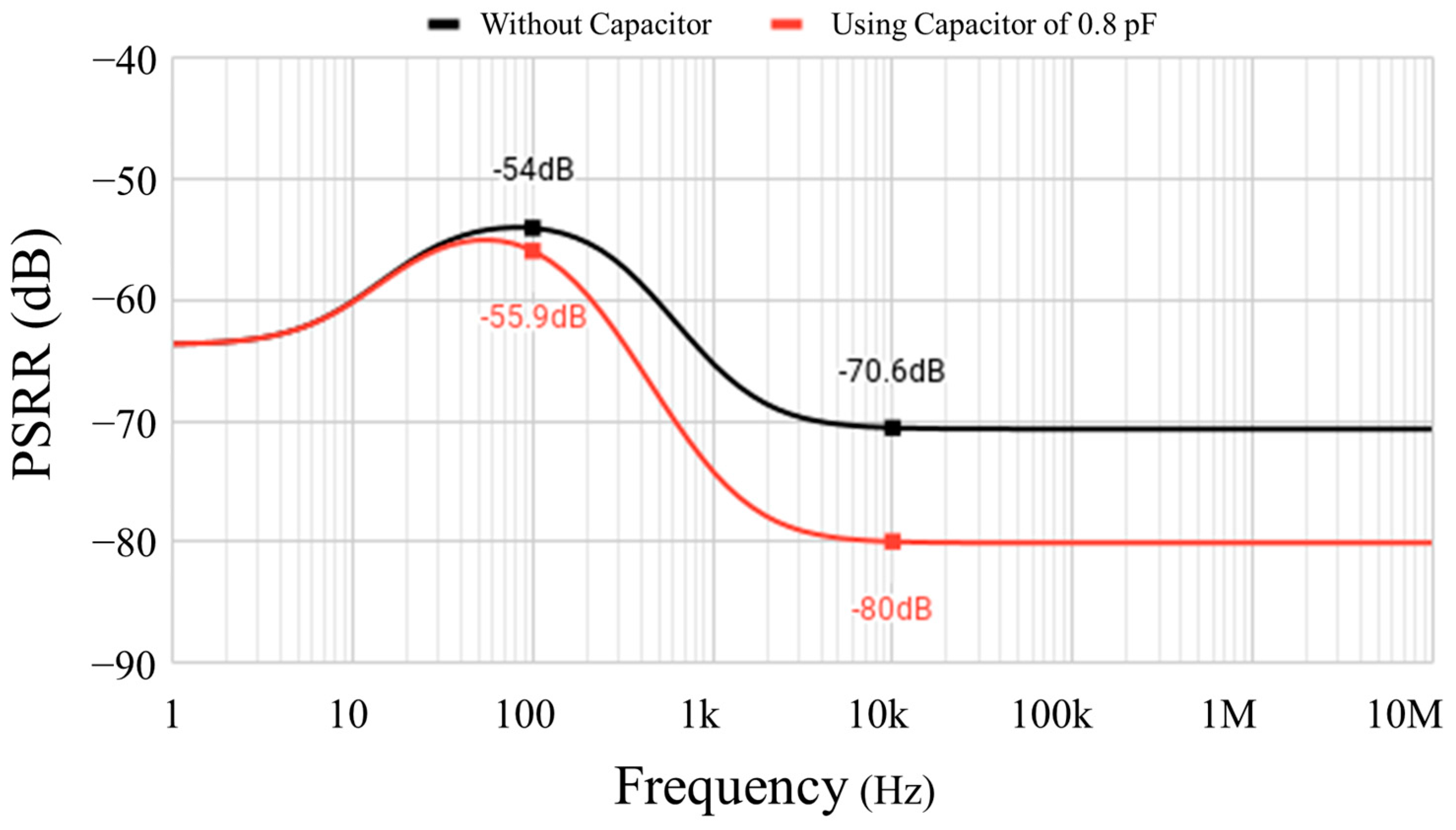
Figure 14 presents the PSRR of the proposed design, with and without a capacitor. The capacitor can be located above the active area, so that it does not occupy an additional space. At a frequency of 100 Hz, a PSRR of −54 dB can be obtained. At frequencies above 8 kHz, the PSRR plateaus at around −70.6 dB. With an additional capacitor of 0.8 pF, a PSRR as low as −80 dB can be attained above 10 kHz.
Table 2 summarizes the performance of the proposed voltage reference and provides a comparison to other references published in recent years, notably the 2-T reference [4] that is employed as the base reference. By performing a simple 4-bit trimming using the results of the 400-point Monte Carlo simulation, the proposed design achieves a LS of 0.035 %/V, the lowest among the sub-nW voltage references. In addition, compared to another design adopting DIBL compensation [7], the proposed design occupies 10-fold less area.
6. Conclusions
This paper presented an ultra-low-power CMOS voltage reference with an LS improvement technique using DIBL-effect cancellation without additional self-bias feedback loops or start-up circuits. The simulation results in 180 nm CMOS show that the circuit generates a reference voltage of 307.8 mV, while consuming only 21.4 pW of power at nominal conditions. According to 400-point Monte Carlo simulations, the worst case LS of 0.035 %/V is achieved across numerous process and mismatch variations after a 4-bit trimming circuit. The simulated PSRR is -54 dB at the worst condition of 100 Hz and at a minimum operating supply of 0.6 V. The proposed design is well-suited for energy-constrained systems, such as battery-operated IoT devices, thanks to its ultra-low power and superior accuracy characteristics.
Author Contributions
Conceptualization, L.C., T.J. and Y.J.; methodology, L.C., T.J. and Y.J.; software, L.C. and Y.J.; validation, L.C., T.J. and Y.J.; formal analysis, L.C., T.J. and Y.J.; investigation, L.C., T.J. and Y.J.; resources, T.J.; data curation, L.C. and Y.J.; writing—original draft preparation, L.C. and Y.J.; writing—review and editing, T.J. and Y.J.; visualization, L.C. and Y.J.; supervision, T.J. and Y.J.; project administration, T.J. and Y.J. All authors have read and agreed to the published version of the manuscript.
Funding
These results was in part supported by the “Regional Innovation Strategy (RIS)” through the National Research Foundation of Korea(NRF), funded by the Ministry of Education(MOE)(2021RIS-004). This research was in part supported by the MSIT (Ministry of Science and ICT), Korea, under the ICAN (ICT Challenge and Advanced Network of HRD) program (IITP-2023-RS-2022-00156212), supervised by the IITP (Institute of Information & Communications Technology Planning & Evaluation).
Institutional Review Board Statement
Not applicable.
Informed Consent Statement
Not applicable.
Data Availability Statement
Not applicable.
Conflicts of Interest
The authors declare no conflict of interest.
References
- Chen, K.; Petruzzi, L.; Hulfachor, R.; Onabajo, M. A 1.16-V 5.8-to-13.5-ppm/°C Curvature-Compensated CMOS Bandgap Reference Circuit With a Shared Offset-Cancellation Method for Internal Amplifiers. IEEE J. Solid-State Circuits 2021, 56, 267–276. [Google Scholar] [CrossRef]
- Boo, J.-H.; Cho, K.-I.; Kim, H.-J.; Lim, J.-G.; Kwak, Y.-S.; Lee, S.-H.; Ahn, G.-C. A Single-Trim Switched Capacitor CMOS Bandgap Reference With a 3σ Inaccuracy of +0.02%, −0.12% for Battery-Monitoring Applications. IEEE J. Solid-State Circuits 2021, 56, 1197–1206. [Google Scholar] [CrossRef]
- Kim, M.; Cho, S. A Single BJT Bandgap Reference with Frequency Compensation Exploiting Mirror Pole. IEEE J. Solid-State Circuits 2021, 56, 2902–2912. [Google Scholar] [CrossRef]
- Seok, M.; Kim, G.; Blaauw, D.; Sylvester, D. A PorTable 2-Transistor Picowatt Temperature-Compensated Voltage Reference Operating at 0.5 V. IEEE J. Solid-State Circuits 2012, 47, 2534–2545. [Google Scholar] [CrossRef]
- Lin, J.; Wang, L.; Zhan, C.; Lu, Y. A 1-nW Ultra-Low Voltage Subthreshold CMOS Voltage Reference With 0.0154%/V Line Sensitivity. IEEE Trans. Circuits Syst. II Express Briefs 2019, 66, 1653–1657. [Google Scholar] [CrossRef]
- De Oliveira, A.C.; Cordova, D.; Klimach, H.; Bampi, S. Picowatt, 0.45–0.6 V Self-Biased Subthreshold CMOS Voltage Reference. IEEE Trans. Circuits Syst. I Regul. Pap. 2017, 64, 3036–3046. [Google Scholar] [CrossRef]
- Wang, Y.; Sun, Q.; Luo, H.; Wang, X.; Zhang, R.; Zhang, H. A 48 pW, 0.34 V, 0.019%/V Line Sensitivity Self-Biased Subthreshold Voltage Reference With DIBL Effect Compensation. IEEE Trans. Circuits Syst. I Regul. Pap. 2020, 67, 611–621. [Google Scholar] [CrossRef]
- Lee, I.; Sylvester, D.; Blaauw, D. A Subthreshold Voltage Reference With Scalable Output Voltage for Low-Power IoT Systems. IEEE J. Solid-State Circuits 2017, 52, 1443–1449. [Google Scholar] [CrossRef]
- De Oliveira, A.C.; Cordova, D.; Klimach, H.; Bampi, S. A 0.12–0.4 V, Versatile 3-Transistor CMOS Voltage Reference for Ultra-Low Power Systems. IEEE Trans. Circuits Syst. I Regul. Pap. 2018, 65, 3790–3799. [Google Scholar] [CrossRef]
- Qing, D.; Kaiyuan, Y.; Blaauw, D.; Sylvester, D. A 114-pW PMOS-only, trim-free voltage reference with 0.26% within-wafer inaccuracy for nW systems. In Proceedings of the 2016 IEEE Symposium on VLSI Circuits (VLSI-Circuits), Honolulu, HI, USA, 15–17 June 2016; pp. 1–2. [Google Scholar]
- Mu, S.; Chan, P.K. Design of Precision-Aware Subthreshold-Based MOSFET Voltage Reference. Sensors 2022, 22, 9466. [Google Scholar] [CrossRef] [PubMed]
- Shao, C.-Z.; Kuo, S.-C.; Liao, Y.-T. A 1.8-nW, −73.5-dB PSRR, 0.2-ms Startup Time, CMOS Voltage Reference With Self-Biased Feedback and Capacitively Coupled Schemes. IEEE J. Solid-State Circuits 2021, 56, 1795–1804. [Google Scholar] [CrossRef]
- Fassio, L.; Lin, L.; De Rose, R.; Lanuzza, M.; Crupi, F.; Alioto, M. Trimming-Less Voltage Reference for Highly Uncertain Harvesting Down to 0.25 V, 5.4 pW. IEEE J. Solid-State Circuits 2021, 56, 3134–3144. [Google Scholar] [CrossRef]
- Wang, H.; Mercier, P.P. A 420 fW self-regulated 3T voltage reference generator achieving 0.47%/V line regulation from 0.4-to-1.2 V. In Proceedings of the 2017 IEEE European Solid State Circuits Conference (ESSCIRC), Leuven, Belgium, 11–14 September 2017; pp. 15–18. [Google Scholar]
- Grotjohn, T.; Hoefflinger, B. A parametric short-channel MOS transistor model for subthreshold and strong inversion current. IEEE J. Solid-State Circuits 1984, 19, 100–112. [Google Scholar] [CrossRef]
Figure 1.
Simulated drain current of different-length PMOS transistors in 180 nm as a function of the drain-source voltage with and mV for all cases [7].
Figure 1.
Simulated drain current of different-length PMOS transistors in 180 nm as a function of the drain-source voltage with and mV for all cases [7].

Figure 2.
Schematic of the proposed voltage reference circuit.

Figure 3.
Simulated current biasing of M2.

Figure 4.
Linearity of the intermediate voltages and .

Figure 5.
Line sensitivity depending on the width of M4.

Figure 6.
Schematic of the proposed circuit, including trimming for minimum line sensitivity.

Figure 7.
Simulated variation of versus in the suggested operating range of .

Figure 8.
Simulated output voltage of the proposed voltage reference in comparison with the conventional 2-T reference.
Figure 8.
Simulated output voltage of the proposed voltage reference in comparison with the conventional 2-T reference.

Figure 9.
Normalized and magnified output voltages of the proposed design and the conventional 2-T reference.
Figure 9.
Normalized and magnified output voltages of the proposed design and the conventional 2-T reference.

Figure 10.
Monte Carlo simulation results for the line sensitivity of the circuit presented in Figure 2 (400 runs).
Figure 10.
Monte Carlo simulation results for the line sensitivity of the circuit presented in Figure 2 (400 runs).

Figure 11.
Monte Carlo simulation results for the line sensitivity of the circuit presented in Figure 6 using the optimal trimming code for each run (400 runs).
Figure 11.
Monte Carlo simulation results for the line sensitivity of the circuit presented in Figure 6 using the optimal trimming code for each run (400 runs).

Figure 12.
Simulated temperature variation of .

Figure 13.
Simulated power consumption.

Figure 14.
Simulated PSRR at 25 °C and .


Table 1.
MOSFET dimensions of the proposed circuit.
| Transistor | Width (µm) | Length (µm) | Current (pA) |
|---|---|---|---|
| M1 (Native) | 3.2 | 20 | 17 |
| M2 | 10.2 | 20 | 13 |
| M3 | 50 | 20 | 19 |
| M4 | 9.91 | 20 | 4 |
| M5 | 100 | 0.3 | 19 |
| M6 | 100 | 0.3 | 17 |
Table 2.
Performance summary and comparison to other works.
| This Work * | [4] | [5] | [6] | [7] | [8] | [9] | [10] | [11] | [12] | [13] | [14] | |
|---|---|---|---|---|---|---|---|---|---|---|---|---|
| Technology (nm) | 180 | 180 | 180 | 180 | 180 | 180 | 130 | 180 | 40 | 180 | 180 | 65 |
| VDD (V) | 0.6~1.8 | 0.5~3.6 | 0.4~1.8 | 0.45~3.3 | 0.34~1.8 | 1.4~3.6 | 0.3~1.2 | 1.2~2.2 | 1.2~1.8 | 0.9~1.8 | 0.25~1.8 | 0.4~1.2 |
| VREF (V) | 0.3078 | 0.3284 | 0.151 | 0.2566 | 0.1479 | 1.25 | 0.026 | 0.9862 | 0.8 | 0.261 | 0.094 | 0.3428 |
| Temp. Range (°C) | −20~80 | −20~80 | −40~125 | 0~120 | 0~100 | 0~100 | −25~125 | −40~85 | −40~90 | −40~130 | 0~120 | −40~60 |
| TC (ppm/°C) | 24.8 | 115.3 | 89.83 | 72.4 | 14.8 | 31 | 208 | 86 | 3 | 62 | 265 | 252.2 |
| LS (%/V) | 0.020 | 0.044 | 0.163 | 0.15 | 0.019 | 0.31 | 0.188 | 0.38 | 0.028 | 0.013 | 0.16 | 0.47 |
| Worst LS (%/V) | 0.035 | N/A | N/A | N/A | 0.039 * | N/A | N/A | N/A | N/A | N/A | 0.31 | N/A |
| # of Samples | 400 | 14 | 16 | 5 | 39 400 * | 60 | 5 | 60 | 200 | 15 | 30 | 38 |
| PSRR @ 100 Hz (dB) | −54 | −49 | −55 | −43.9 | −63 | −41 | −67.3 * | −42 | −71.7 | −73.5 | −70 | N/A |
| Power @ 25 °C (pW) | 21.4 | 5.5 | 1000 | 147 | 48 | 33.6 | 40 | 114 | 9600000 | 1800 | 5.4 | 0.42 @ 20 °C |
| Area (mm2) | 0.003 | 0.001425 | 0.005 | 0.002 | 0.0332 | 0.0025 | 0.0006 | 0.00488 | N/A | 0.0059 | 0.0022 | 0.00010 |
* Simulation Result.
Disclaimer/Publisher’s Note: The statements, opinions and data contained in all publications are solely those of the individual author(s) and contributor(s) and not of MDPI and/or the editor(s). MDPI and/or the editor(s) disclaim responsibility for any injury to people or property resulting from any ideas, methods, instructions or products referred to in the content. |
© 2023 by the authors. Licensee MDPI, Basel, Switzerland. This article is an open access article distributed under the terms and conditions of the Creative Commons Attribution (CC BY) license (https://creativecommons.org/licenses/by/4.0/).
Share and Cite
MDPI and ACS Style
Colbach, L.; Jang, T.; Ji, Y. A 21.4 pW Subthreshold Voltage Reference with 0.020 %/V Line Sensitivity Using DIBL Compensation. Sensors 2023, 23, 1862. https://doi.org/10.3390/s23041862
AMA Style
Colbach L, Jang T, Ji Y. A 21.4 pW Subthreshold Voltage Reference with 0.020 %/V Line Sensitivity Using DIBL Compensation. Sensors. 2023; 23(4):1862. https://doi.org/10.3390/s23041862
Chicago/Turabian StyleColbach, Louis, Taekwang Jang, and Youngwoo Ji. 2023. "A 21.4 pW Subthreshold Voltage Reference with 0.020 %/V Line Sensitivity Using DIBL Compensation" Sensors 23, no. 4: 1862. https://doi.org/10.3390/s23041862
Note that from the first issue of 2016, this journal uses article numbers instead of page numbers. See further details here.