
Nanoscale Characterization of Graphene Oxide-Based Epoxy Nanocomposite Using Inverted Scanning Microwave Microscopy

 , , , ,
  , , , ,
  , , and
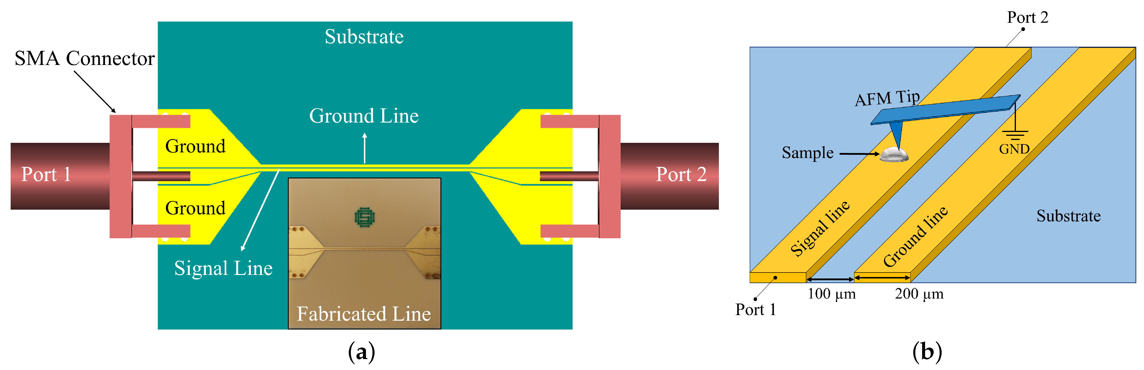
Abstract
:1. Introduction
2. Materials and Methods
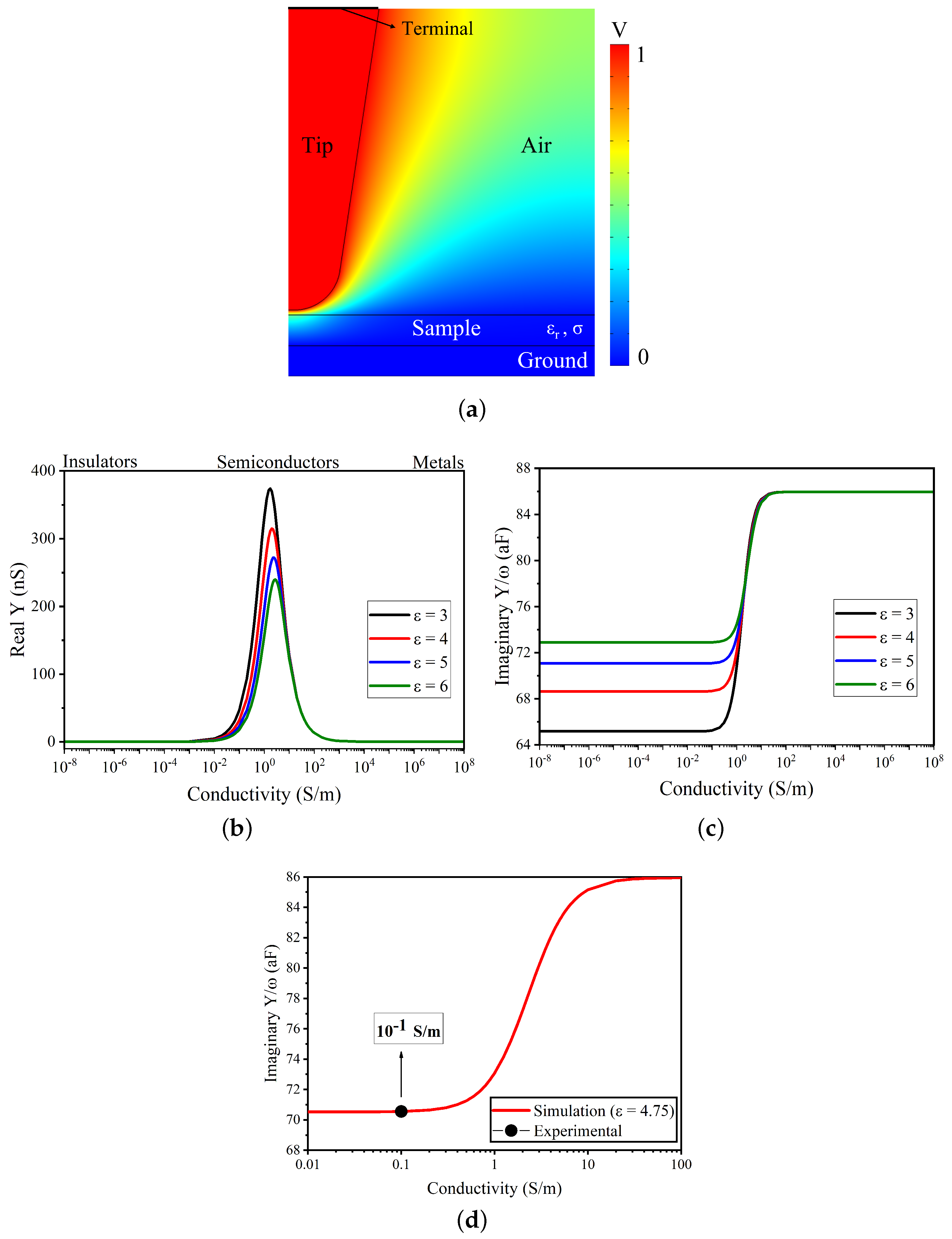
2.1. Experimental Setup
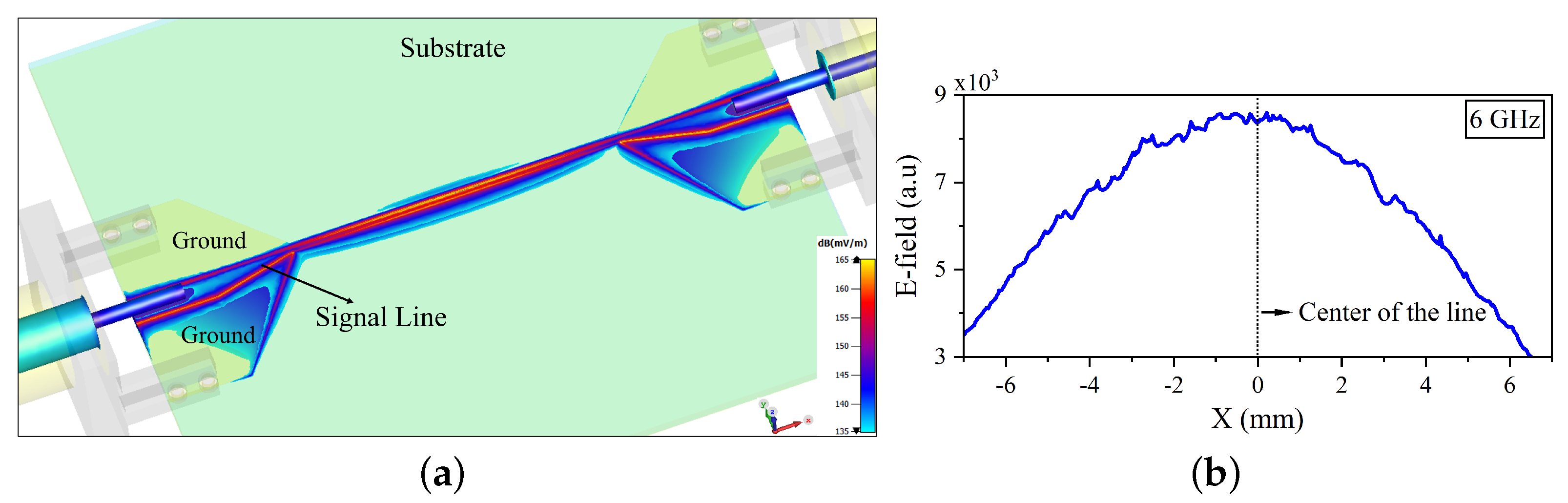
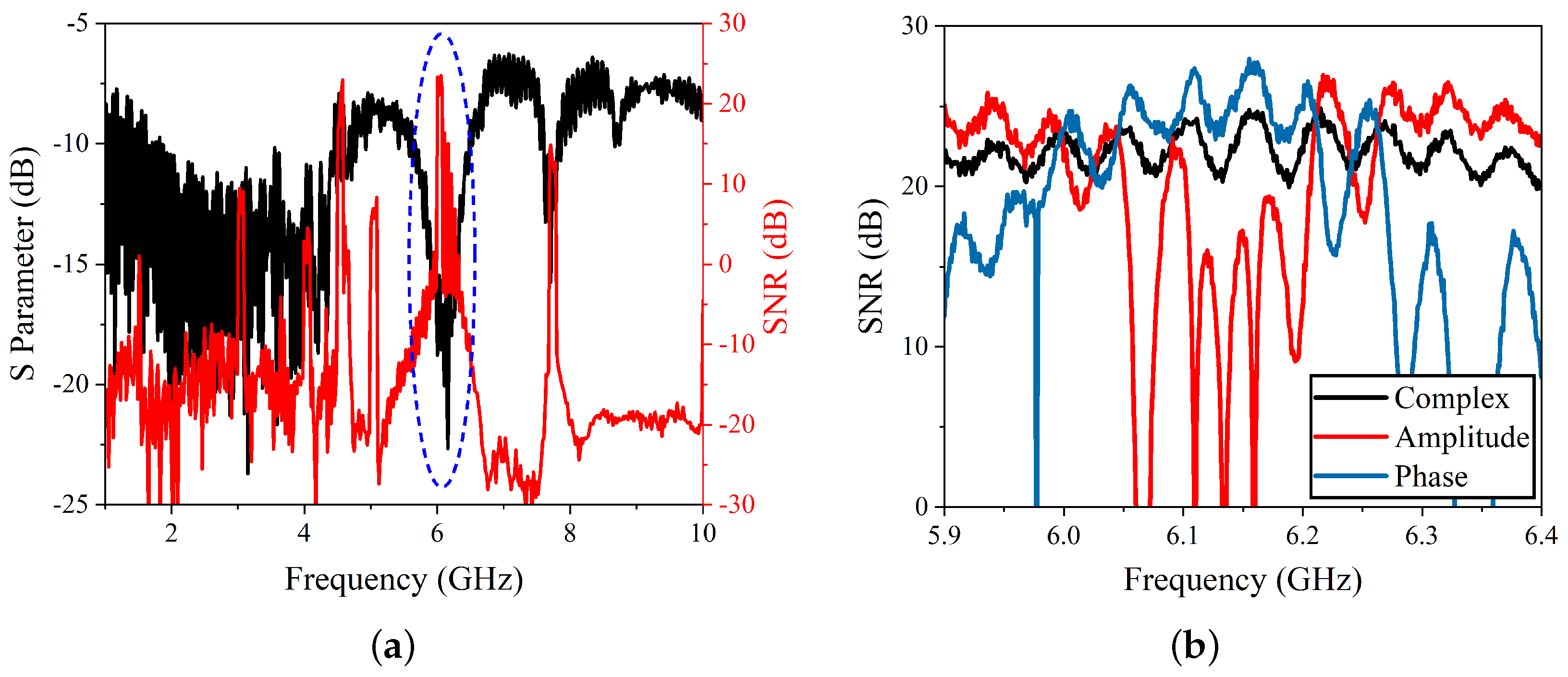
2.2. Sensitivity of the iSMM System
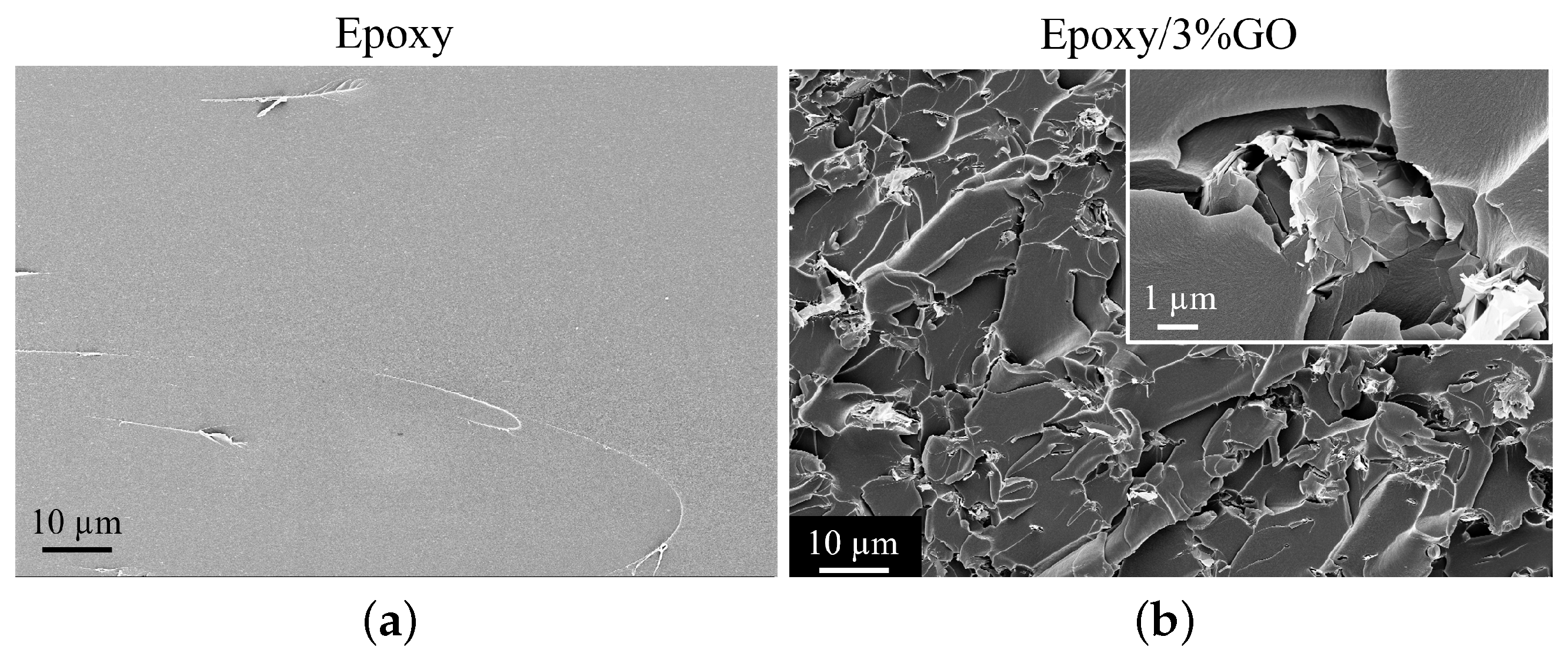
2.3. Sample and Microstructure Analysis
3. Results and Discussion
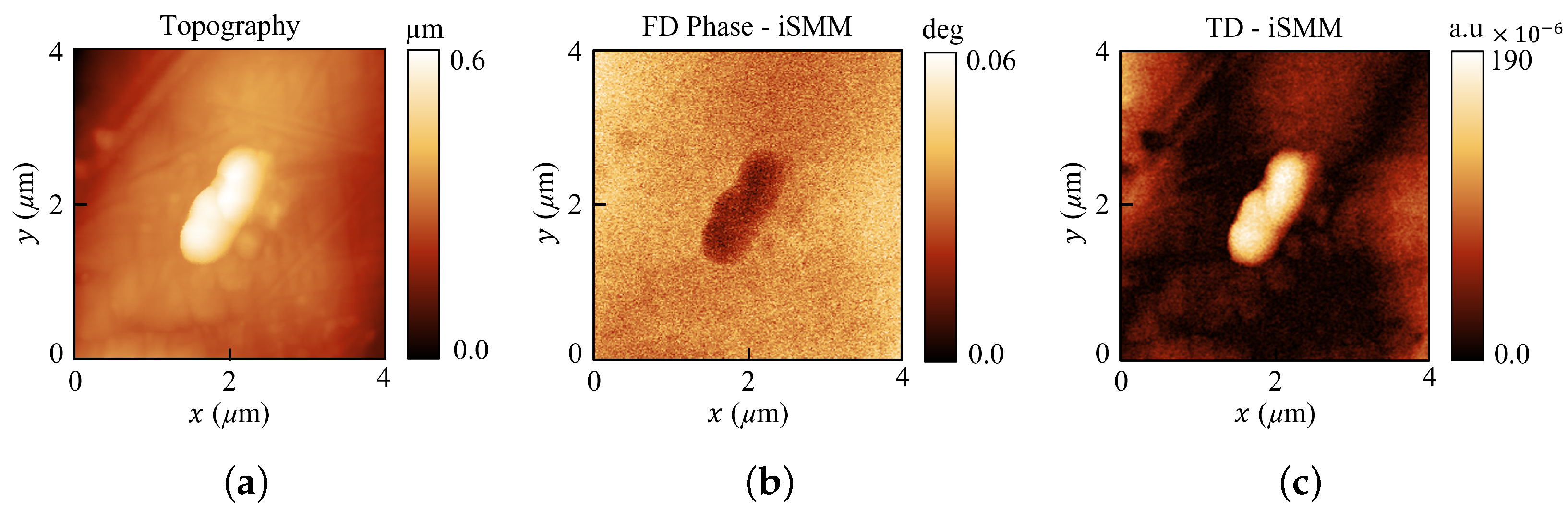
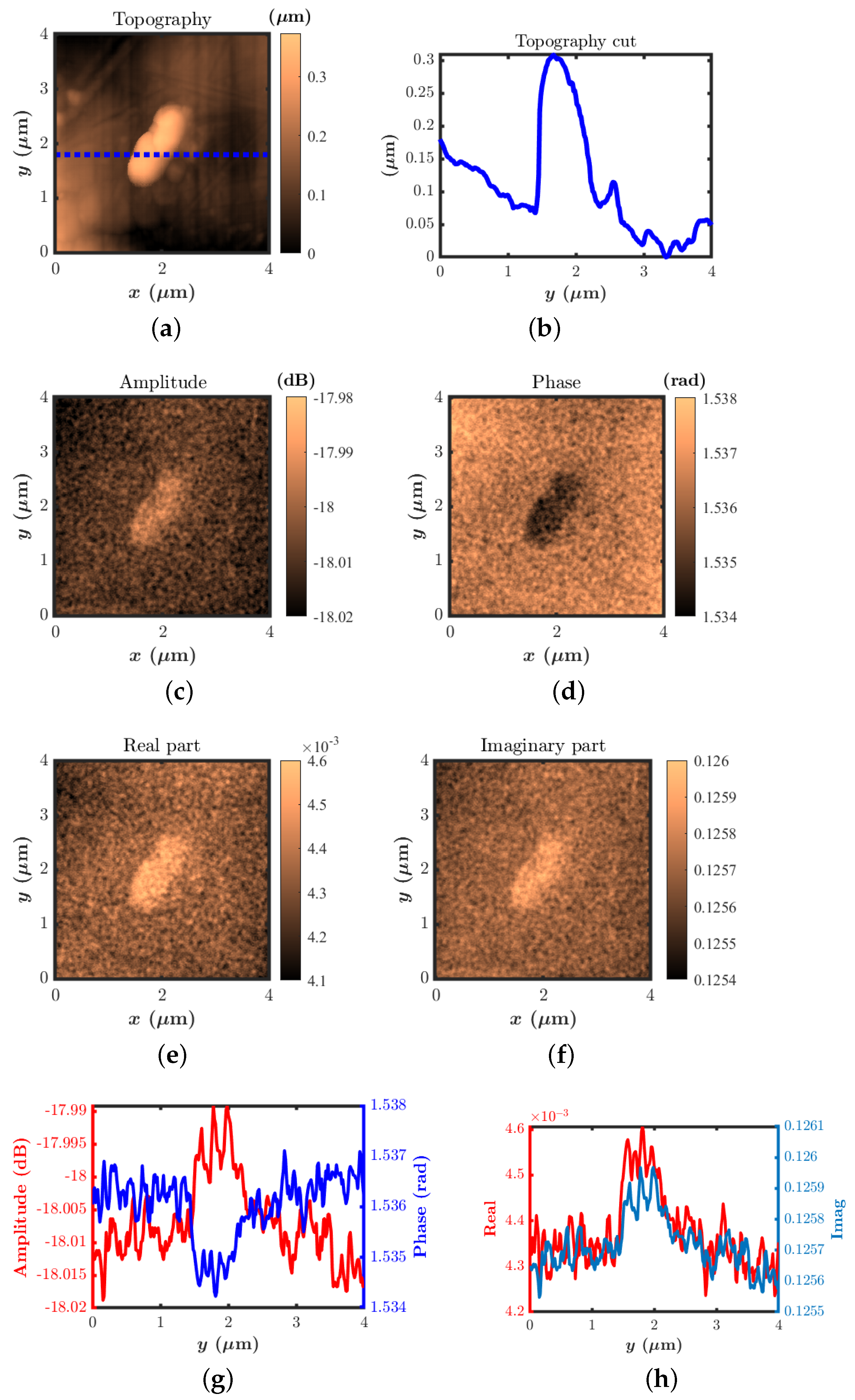
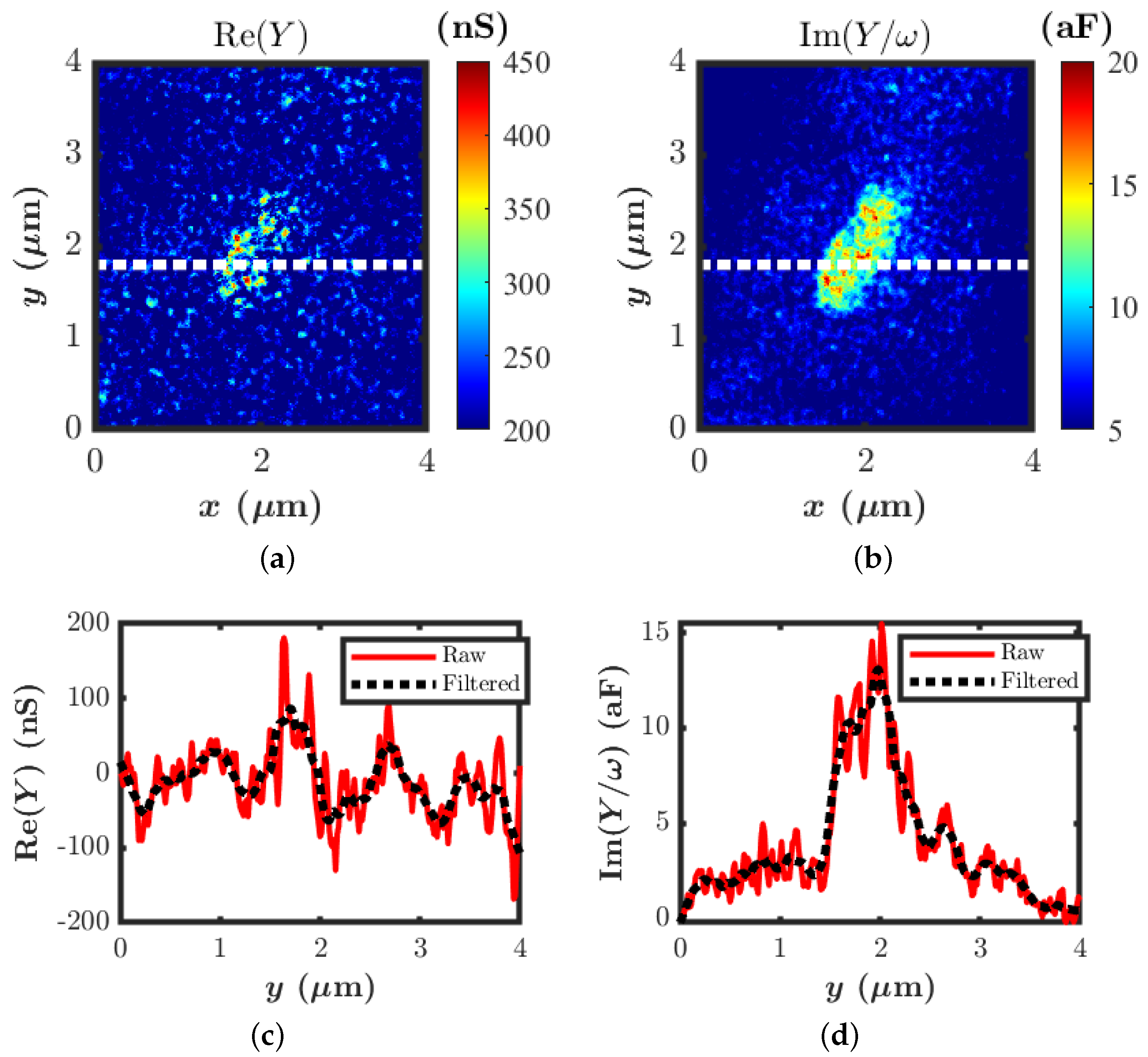
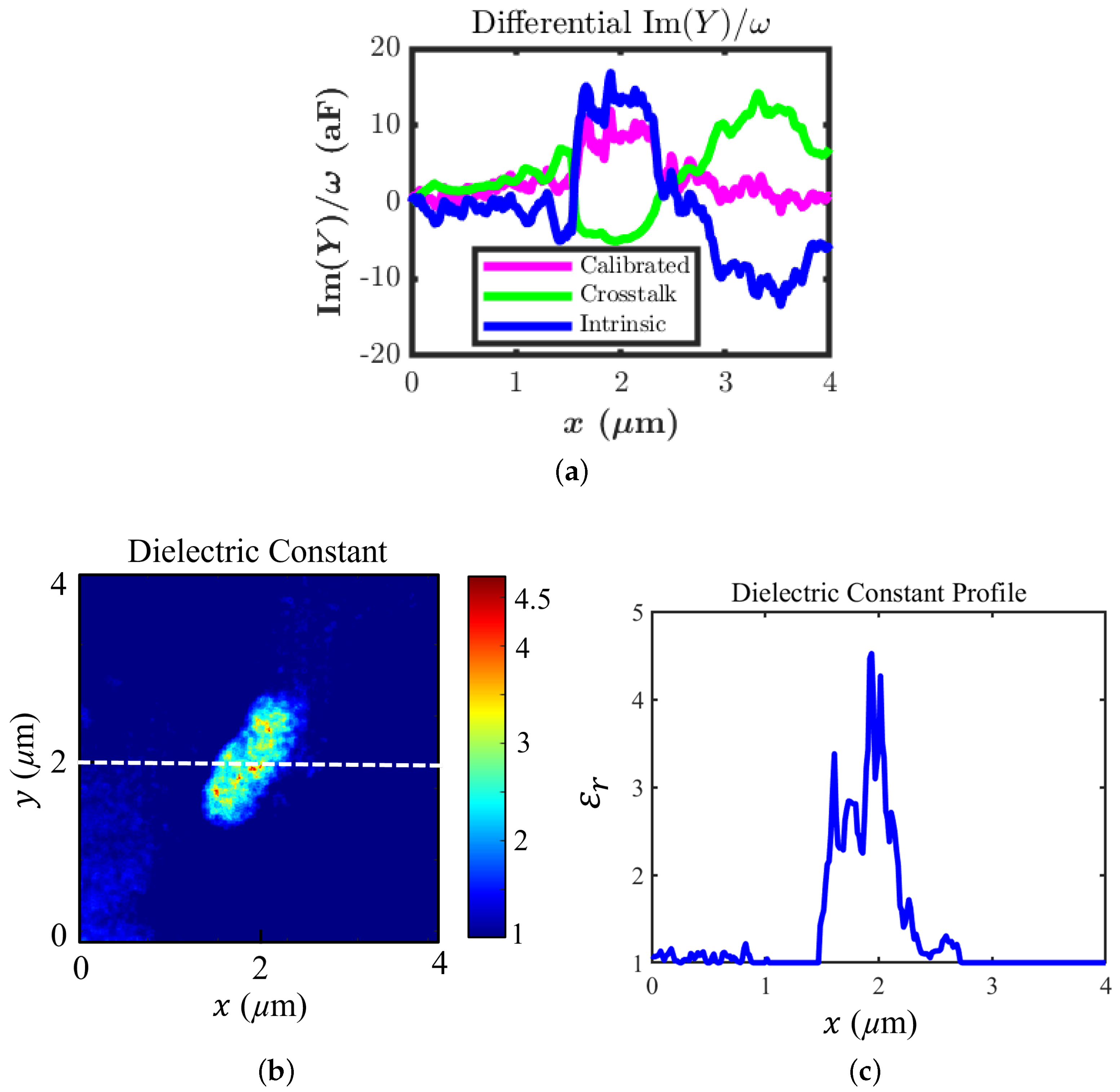
3.1. iSMM Imaging
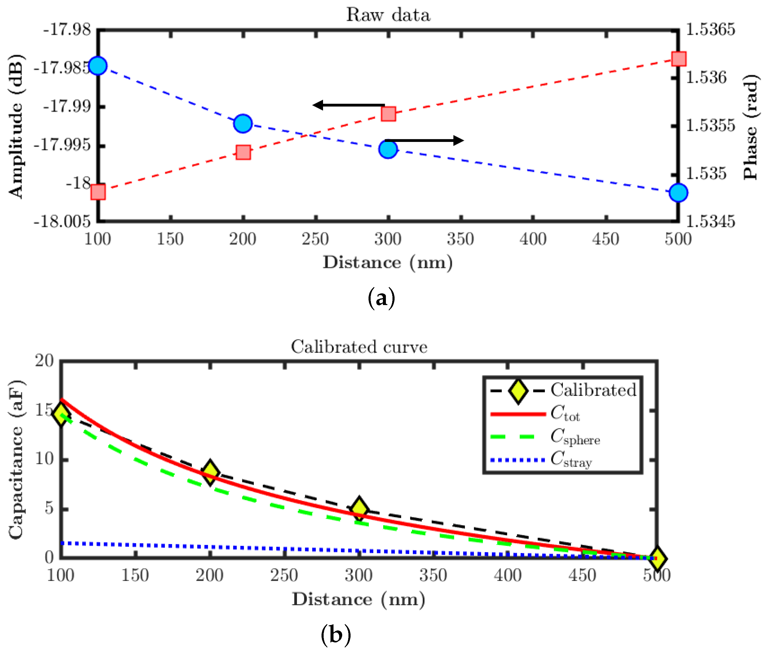
3.2. iSMM Calibration
4. Conclusions
Author Contributions
Funding
Institutional Review Board Statement
Informed Consent Statement
Data Availability Statement
Acknowledgments
Conflicts of Interest
References
- Siegel, P.H.T. Microwaves Are Everywhere: “SMM: Nano-Microwaves”. IEEE J. Microwaves 2021, 1, 838–852. [Google Scholar] [CrossRef]
- Anlage, S.M.; Talanov, V.V.; Schwartz, A.R. Principles of Near-Field Microwave Microscopy. In Scanning Probe Microscopy: Electrical and Electromechanical Phenomena at the Nanoscale; Kalinin, S., Gruverman, A., Eds.; Springer: New York, NY, USA, 2007; pp. 215–253. [Google Scholar]
- Imtiaz, A.; Anlage, S.M. A novel STM-assisted microwave microscope with capacitance and loss imaging capability. Ultramicroscopy 2003, 94, 209–216. [Google Scholar] [CrossRef] [PubMed]
- Tabib-Azar, M.; Wang, Y. Design and fabrication of scanning near-field microwave probes compatible with atomic force microscopy to image embedded nanostructures. IEEE Trans. Microwave Theory Tech. 2004, 52, 971–979. [Google Scholar] [CrossRef]
- Karbassi, A.; Ruf, D.; Bettermann, A.D.; Paulson, C.A.; van der Weide, D.W.; Tanbakuchi, H.; Stancliff, R. Quantitative Scanning Near-Field Microwave Microscopy for Thin Film Dielectric Constant Measurement. Rev. Sci. Instrum. 2008, 79, 094706. [Google Scholar] [CrossRef] [PubMed]
- Gramse, G.; Kasper, M.; Fumagalli, L.; Gomila, G.; Hinterdorfer, P.; Kienberger, F. Calibrated complex impedance and permittivity measurements with scanning microwave microscopy. Nanotechnology 2014, 25, 145703. [Google Scholar] [CrossRef] [PubMed]
- Introduction to Scanning Microwave Microscopy (SMM) Mode. Available online: http://literature.cdn.keysight.com/litweb/pdf/5989-8881EN.pdf (accessed on 30 October 2022).
- Imtiaz, A.; Wallis, T.M.; Kabos, P. Near-Field Scanning Microwave Microscopy: An Emerging Research Tool for Nanoscale Metrology. IEEE Microw. Mag. 2014, 15, 52–64. [Google Scholar] [CrossRef]
- Farina, M.; Hwang, J.C.; Di Donato, A.; Pavoni, E.; Fabi, G.; Morini, A.; Piacenza, F.; Di Filippo, E.; Pietrangelo, T. Imaging of sub-cellular structures and organelles by an STM-assisted scanning microwave microscope at mm-waves. In Proceedings of the IEEE/MTT-S International Microwave Symposium (IMS), Philadelphia, PA, USA, 10–15 June 2018; pp. 111–114. [Google Scholar]
- Farina, M.; Piacenza, F.; De Angelis, F.; Mencarelli, D.; Morini, A.; Venanzoni, G.; Pietrangelo, T.; Malavolta, M.; Basso, A.; Provinciali, M.; et al. Investigation of fullerene exposure of breast cancer cells by time-gated scanning microwave microscopy. IEEE Trans. Microw. Theory Tech. 2016, 64, 4823–4831. [Google Scholar] [CrossRef]
- Pavoni, E.; Yivlialin, R.; Joseph, C.H.; Fabi, G.; Mencarelli, D.; Pierantoni, L.; Bussetti, G.; Farina, M. Blisters on graphite surface: A scanning microwave microscopy investigation. RSC Adv. 2019, 9, 23156–23160. [Google Scholar] [CrossRef] [Green Version]
- Farina, M.; Jin, X.; Fabi, G.; Pavoni, E.; Di Donato, A.; Mencarelli, D.; Morini, A.; Piacenza, F.; Al Hadi, R.; Zhao, Y.; et al. Inverted scanning microwave microscope for in vitro imaging and characterization of biological cells. Appl. Phys. Lett. 2019, 114, 093703. [Google Scholar] [CrossRef] [Green Version]
- Farina, M.; Mencarelli, D.; Di Donato, A.; Venanzoni, G.; Morini, A. Calibration protocol for broadband near-field microwave microscopy. IEEE Trans. Microw. Theory Tech. 2011, 59, 2769–2776. [Google Scholar] [CrossRef]
- Farina, M.; Lucesoli, A.; Pietrangelo, T.; di Donato, A.; Fabiani, S.; Venanzoni, G.; Mencarelli, D.; Rozzi, T.; Morini, A. Disentangling time in a near-field approach to scanning probe microscopy. Nanoscale 2011, 3, 3589–3593. [Google Scholar] [CrossRef]
- Fabi, G.; Jin, X.; Hwang, J.C.; Joseph, C.H.; Pavoni, E.; Li, L.; Xiong, K.; Ning, Y.; Mencarelli, D.; di Donato, A.; et al. Inverted scanning microwave microscopy for nanometer-scale imaging and characterization of platinum diselenide. In Proceedings of the IEEE MTT-S International Microwave Symposium (IMS), Boston, MA, USA, 2–7 June 2019; pp. 1115–1117. [Google Scholar]
- Fabi, G.; Jin, X.; Pavoni, E.; Joseph, C.H.; Di Donato, A.; Mencarelli, D.; Wang, X.; Al Hadi, R.; Morini, A.; Hwang, J.C.; et al. Quantitative characterization of platinum diselenide electrical conductivity with an inverted scanning microwave microscope. IEEE Trans. Microw. Theory Tech. 2021, 69, 3348–3359. [Google Scholar] [CrossRef]
- Fabi, G.; Joseph, C.H.; Pavoni, E.; Wang, X.; Al Hadi, R.; Hwang, J.C.; Morini, A.; Farina, M. Real-time removal of topographic artifacts in scanning microwave microscopy. IEEE Trans. Microw. Theory Tech. 2021, 69, 2662–2672. [Google Scholar] [CrossRef]
- Azman, S.A.; Fabi, G.; Pavoni, E.; Joseph, C.H.; Pini, N.; Pietrangelo, T.; Pierantoni, L.; Morini, A.; Mencarelli, D.; Di Donato, A.; et al. Inverted Scanning Microwave Microscopy of a Vital Mitochondrion in Liquid. IEEE Microw. Wirel. Components Lett. 2022, 32, 804–806. [Google Scholar] [CrossRef]
- Grall, S.; Alić, I.; Pavoni, E.; Awadein, M.; Fujii, T.; Müllegger, S.; Farina, M.; Clément, N.; Gramse, G. Attoampere nanoelectrochemistry. Small 2021, 17, 2101253. [Google Scholar] [CrossRef]
- Farina, M.; Hwang, J.C. Scanning microwave microscopy for biological applications: Introducing the state of the art and inverted SMM. IEEE Microw. Mag. 2020, 21, 52–59. [Google Scholar] [CrossRef]
- Chung, D.D.L. Electrical applications of carbon materials. J. Mater. Sci. 2004, 39, 2645–2661. [Google Scholar] [CrossRef]
- Stankovich, S.; Dikin, A.D.; Dommett, H.B.G.; Kohlhaas, M.K.; Zimney, J.E.; Stach, A.E.; Piner, D.R.; Nguyen, T.S.; Ruoff, S.R. Graphene-based composite materials. Nature 2006, 442, 282–286. [Google Scholar] [CrossRef]
- Senis, C.E.; Golosnoy, O.I.; Dulieu-Barton, M.J.; Thomsen, O.T. Enhancement of the electrical and thermal properties of unidirectional carbon fibre/epoxy laminates through the addition of graphene oxide. J. Mater. Sci. 2019, 54, 8955–8970. [Google Scholar] [CrossRef] [Green Version]
- Bianchi, I.; Gentili, S.; Greco, L.; Simoncini, M. Effect of graphene oxide reinforcement on the flexural behavior of an epoxy resin. Procedia CIRP 2022, 112, 602–606. [Google Scholar] [CrossRef]
- Wu, H.; Cheng, L.; Liu, C.; Lan, X.; Zhao, H. Engineering the interface in graphene oxide/epoxy composites using bio-based epoxy-graphene oxide nanomaterial to achieve superior anticorrosion performance. J. Colloid Interface Sci. 2021, 587, 755–766. [Google Scholar] [CrossRef] [PubMed]
- Naebe, M.; Wang, J.; Amini, A.; Khayyam, H.; Hameed, N.; Li, L.H.; Chen, Y.; Fox, B. Mechanical property and structure of covalent functionalised graphene/epoxy nanocomposites. Sci. Rep. 2014, 4, 4375. [Google Scholar] [CrossRef] [PubMed] [Green Version]
- Biagi, M.C.; Badino, G.; Fabregas, R.; Gramse, G.; Fumagalli, L.; Gomila, G. Direct mapping of the electric permittivity of heterogeneous non-planar thin films at gigahertz frequencies by scanning microwave microscopy. Phys. Chem. Chem. Phys. 2017, 19, 3884–3893. [Google Scholar] [CrossRef]


Publisher’s Note: MDPI stays neutral with regard to jurisdictional claims in published maps and institutional affiliations. |
© 2022 by the authors. Licensee MDPI, Basel, Switzerland. This article is an open access article distributed under the terms and conditions of the Creative Commons Attribution (CC BY) license (https://creativecommons.org/licenses/by/4.0/).
Share and Cite
Joseph, C.H.; Luzi, F.; Azman, S.N.A.; Forcellese, P.; Pavoni, E.; Fabi, G.; Mencarelli, D.; Gentili, S.; Pierantoni, L.; Morini, A.; et al. Nanoscale Characterization of Graphene Oxide-Based Epoxy Nanocomposite Using Inverted Scanning Microwave Microscopy. Sensors 2022, 22, 9608. https://doi.org/10.3390/s22249608
Joseph CH, Luzi F, Azman SNA, Forcellese P, Pavoni E, Fabi G, Mencarelli D, Gentili S, Pierantoni L, Morini A, et al. Nanoscale Characterization of Graphene Oxide-Based Epoxy Nanocomposite Using Inverted Scanning Microwave Microscopy. Sensors. 2022; 22(24):9608. https://doi.org/10.3390/s22249608
Chicago/Turabian StyleJoseph, C. H., Francesca Luzi, S. N. Afifa Azman, Pietro Forcellese, Eleonora Pavoni, Gianluca Fabi, Davide Mencarelli, Serena Gentili, Luca Pierantoni, Antonio Morini, and et al. 2022. "Nanoscale Characterization of Graphene Oxide-Based Epoxy Nanocomposite Using Inverted Scanning Microwave Microscopy" Sensors 22, no. 24: 9608. https://doi.org/10.3390/s22249608