Author Contributions
Conceptualization, P.P., H.A. and A.F.; methodology, P.P., H.A., J.P. and M.F.; software, J.P.; validation, P.P., H.A., A.F., J.P. and M.F.; formal analysis, J.P. and M.F.; investigation, P.P., J.P. and M.F.; resources, M.F., S.C., S.A., A.L., G.L. and A.F.; data curation, P.P., J.P. and M.F.; writing—original draft preparation, J.P. and M.F.; writing—review & editing, P.P., H.A., J.P. and M.F.; visualization, J.P. and M.F.; supervision, P.P. and H.A.; project administration, A.F., P.P. and H.A.; funding acquisition, A.F., P.P. and H.A. All authors have read and agreed to the published version of the manuscript.
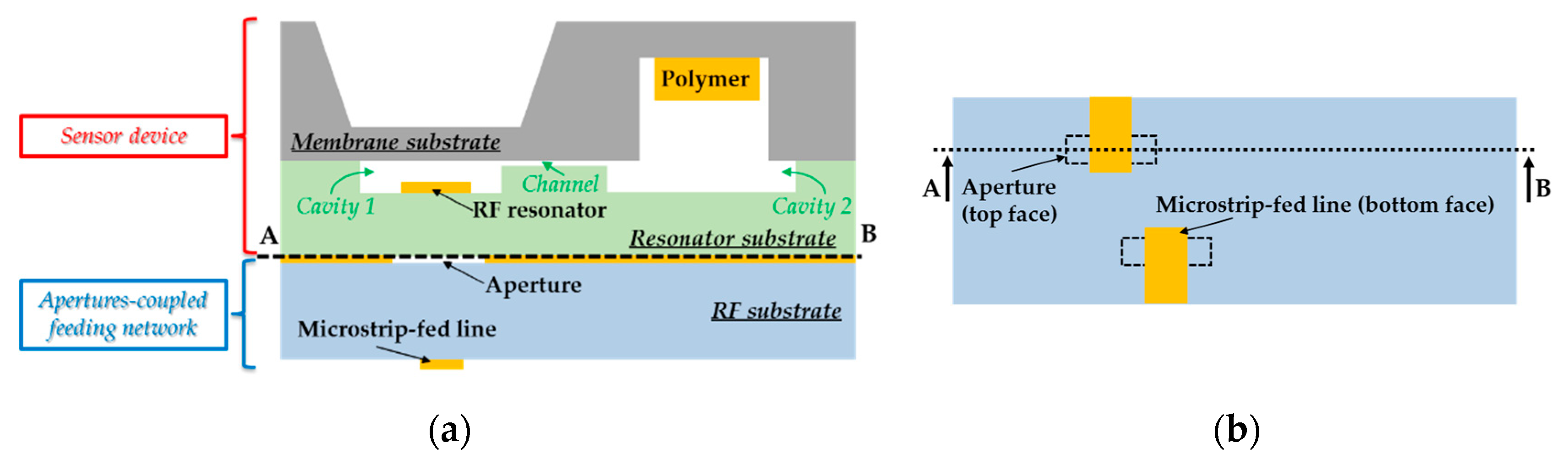
Figure 1.
Cross-sectional view of (
a) the proposed passive microelectromechanical dosimeter and (
b) its bottom view showing the microstrip line used to feed the two-port planar resonator through two small apertures by electromagnetic waves (see [
37,
38]). (
c) The mechanical MEMS transducer studied specifically in this paper.
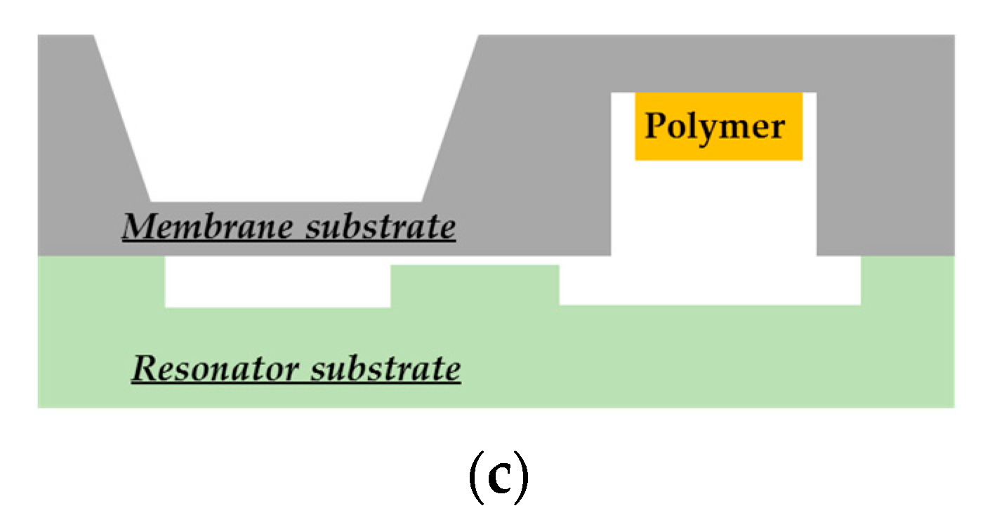
Figure 2.
Molecular structure of (
a) high-density polyethylene (HDPE) and (
b) low-density polyethylene (LDPE) [
30].
Figure 2.
Molecular structure of (
a) high-density polyethylene (HDPE) and (
b) low-density polyethylene (LDPE) [
30].
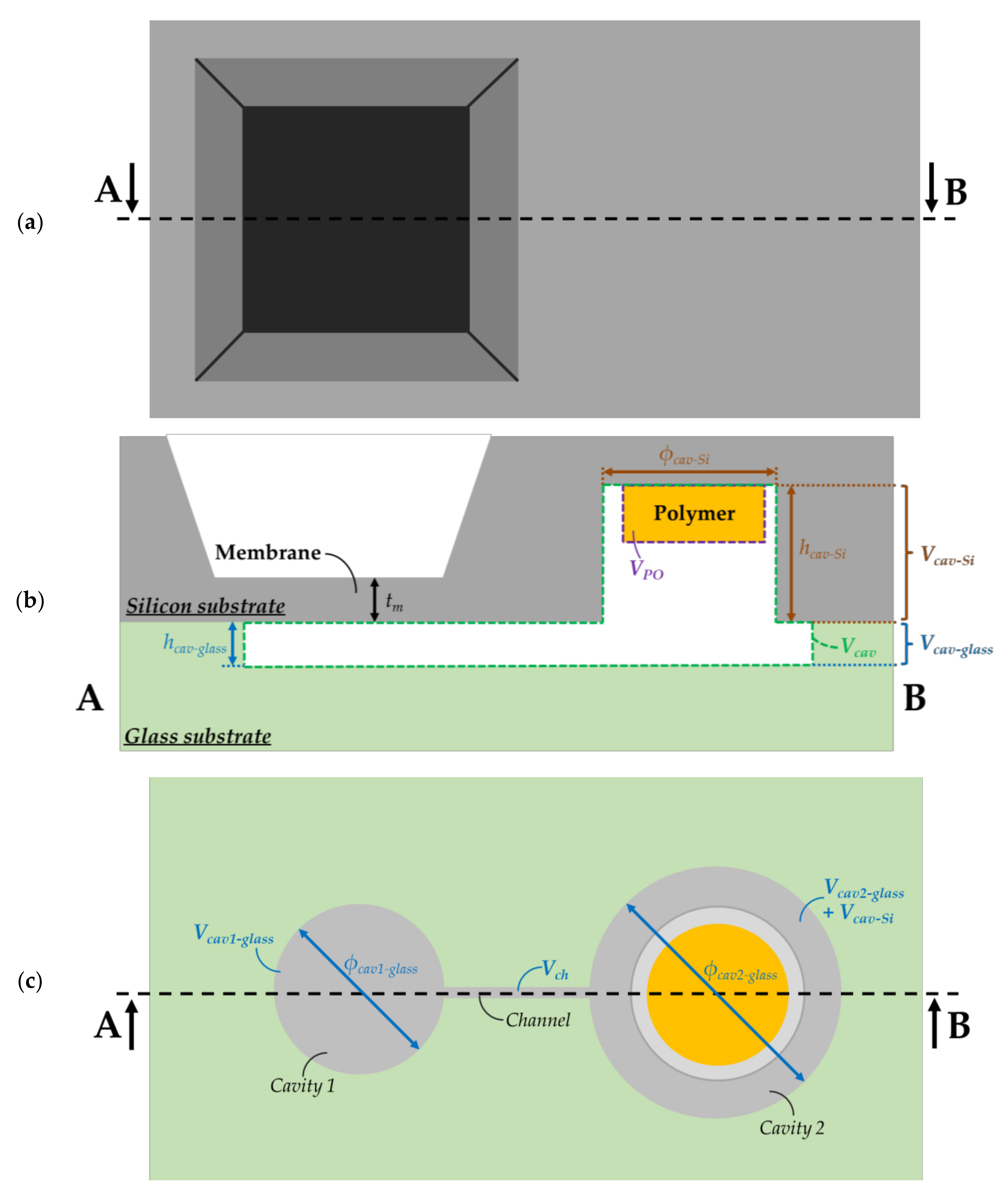
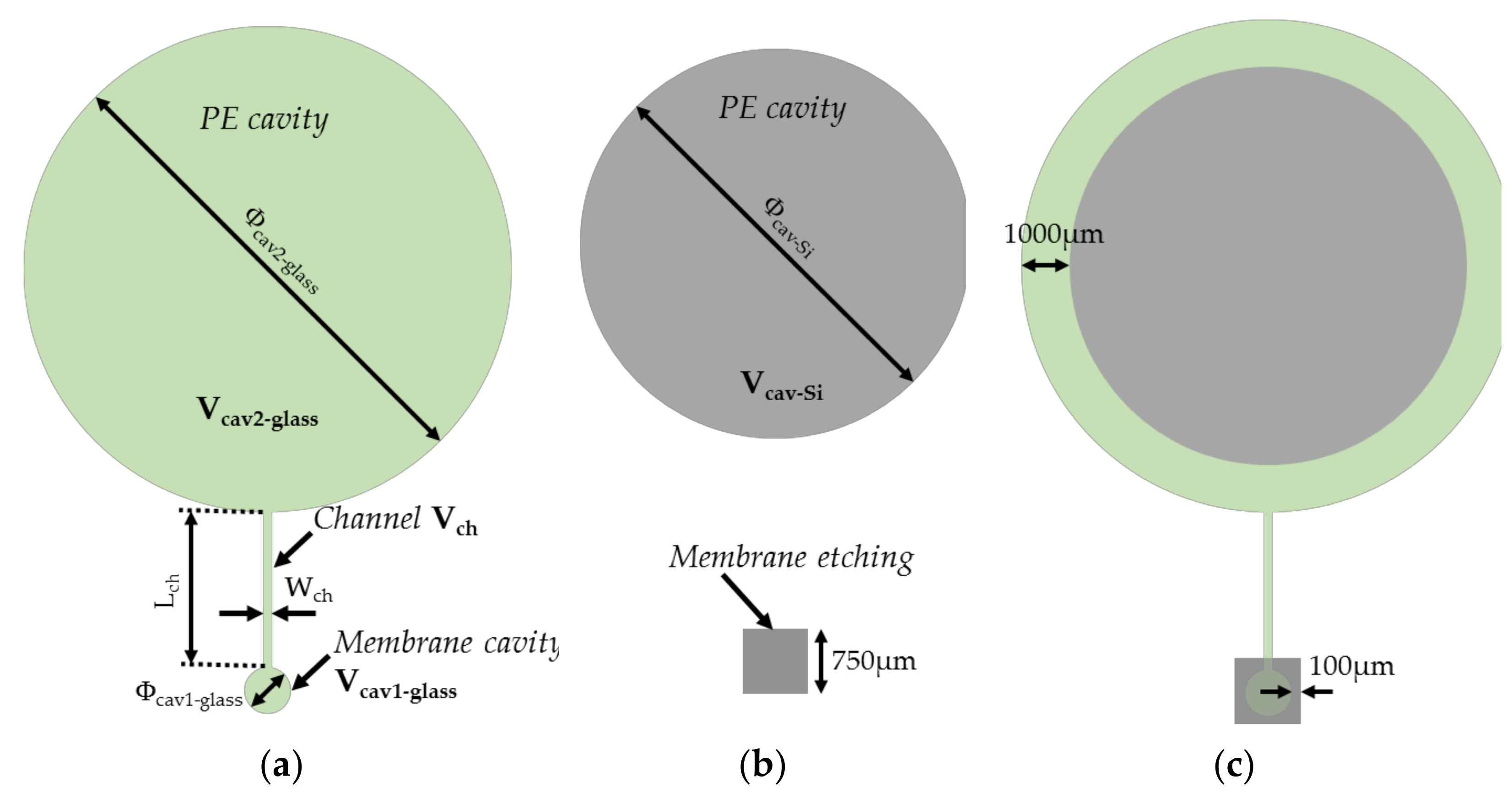
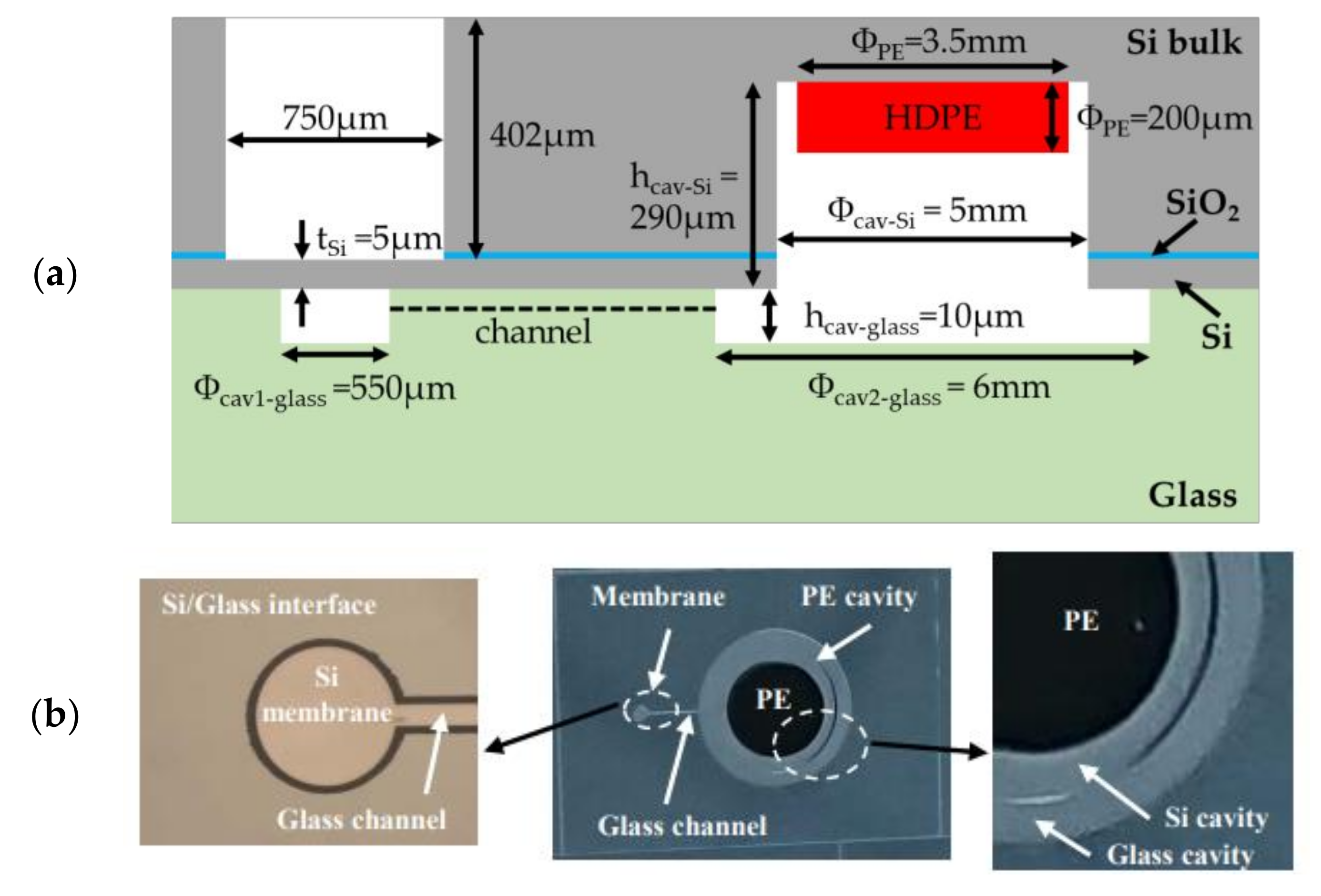
Figure 3.
(a) Top (i.e., from the silicon structure) (b) cross-sectional and (c) bottom (i.e., from the glass substrate) view of the investigated microelectromechanical transducer with different volumes. The total sealed structure of volume includes two cavities etched in the silicon and the glass substrates. These cavities are linked by a channel of volume . , and are, respectively, the volume, height and diameter of the circular cavity (cavity 1) placed below the membrane of thickness . The second cavity (cavity 2) of volume is patterned on the silicon substrate and glass substrate. denotes the cavity diameter in the glass substrate, while denotes the diameter in the silicon substrate and is the height of the cavity in the Si substrate. designates the polymer volume.
Figure 4.
Layouts of the structure on (a) the glass substrate and (b) the silicon substrate; (c) superposition of the two layouts.
Figure 4.
Layouts of the structure on (a) the glass substrate and (b) the silicon substrate; (c) superposition of the two layouts.
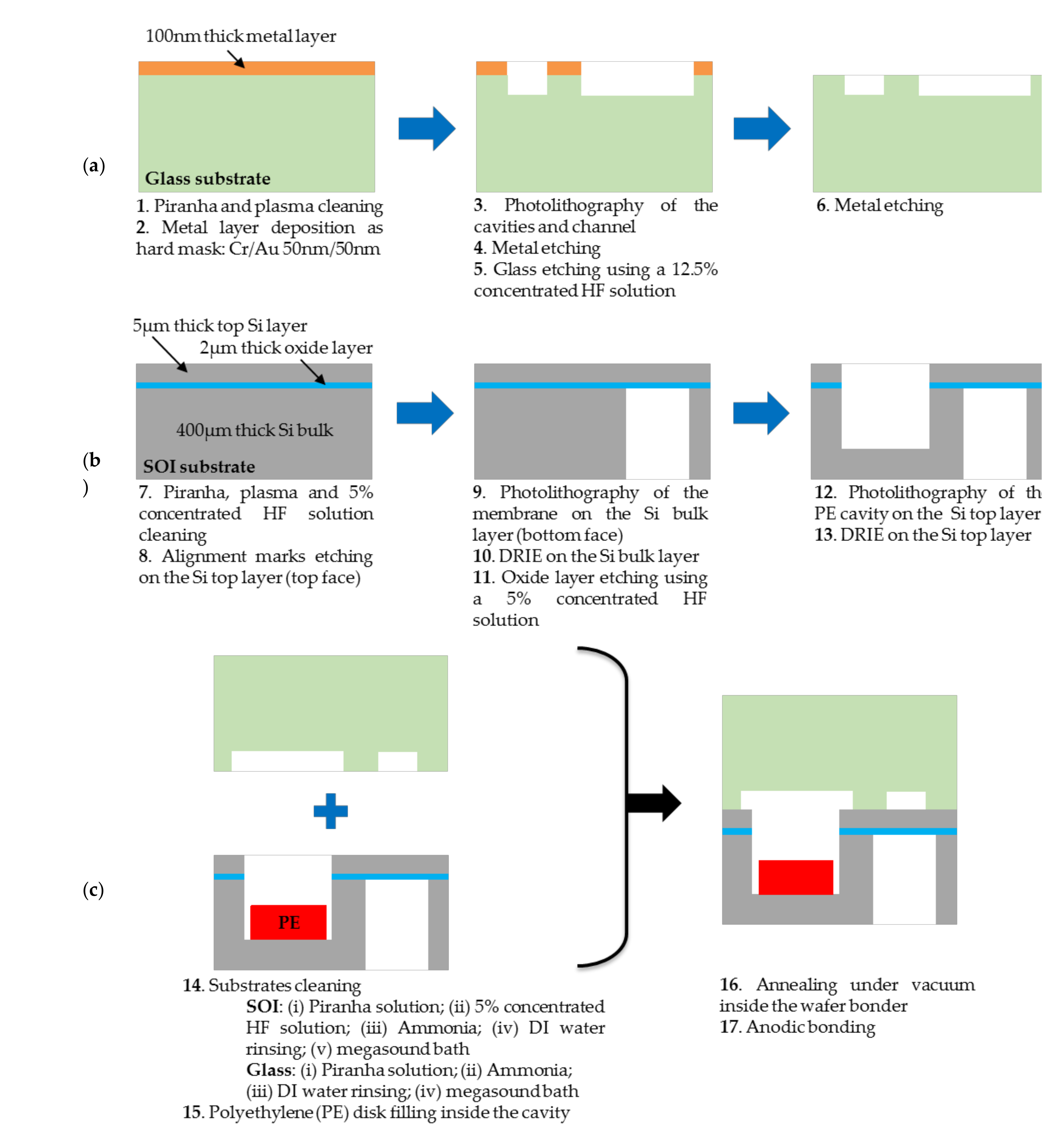
Figure 5.
Steps of the fabrication process for manufacturing of (a) the glass substrate, (b) the silicon substrate and (c) final anodic bonding.
Figure 5.
Steps of the fabrication process for manufacturing of (a) the glass substrate, (b) the silicon substrate and (c) final anodic bonding.
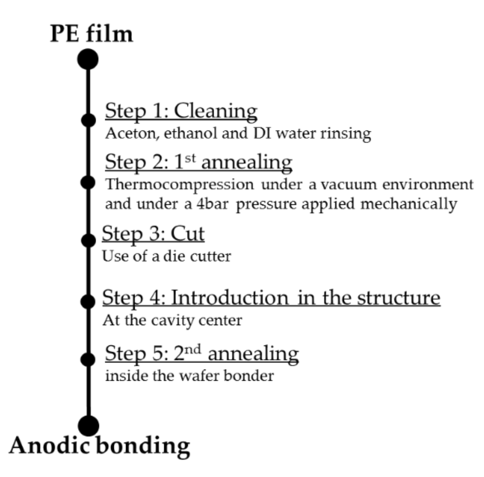
Figure 6.
Polyethylene manufacturing process.
Figure 6.
Polyethylene manufacturing process.
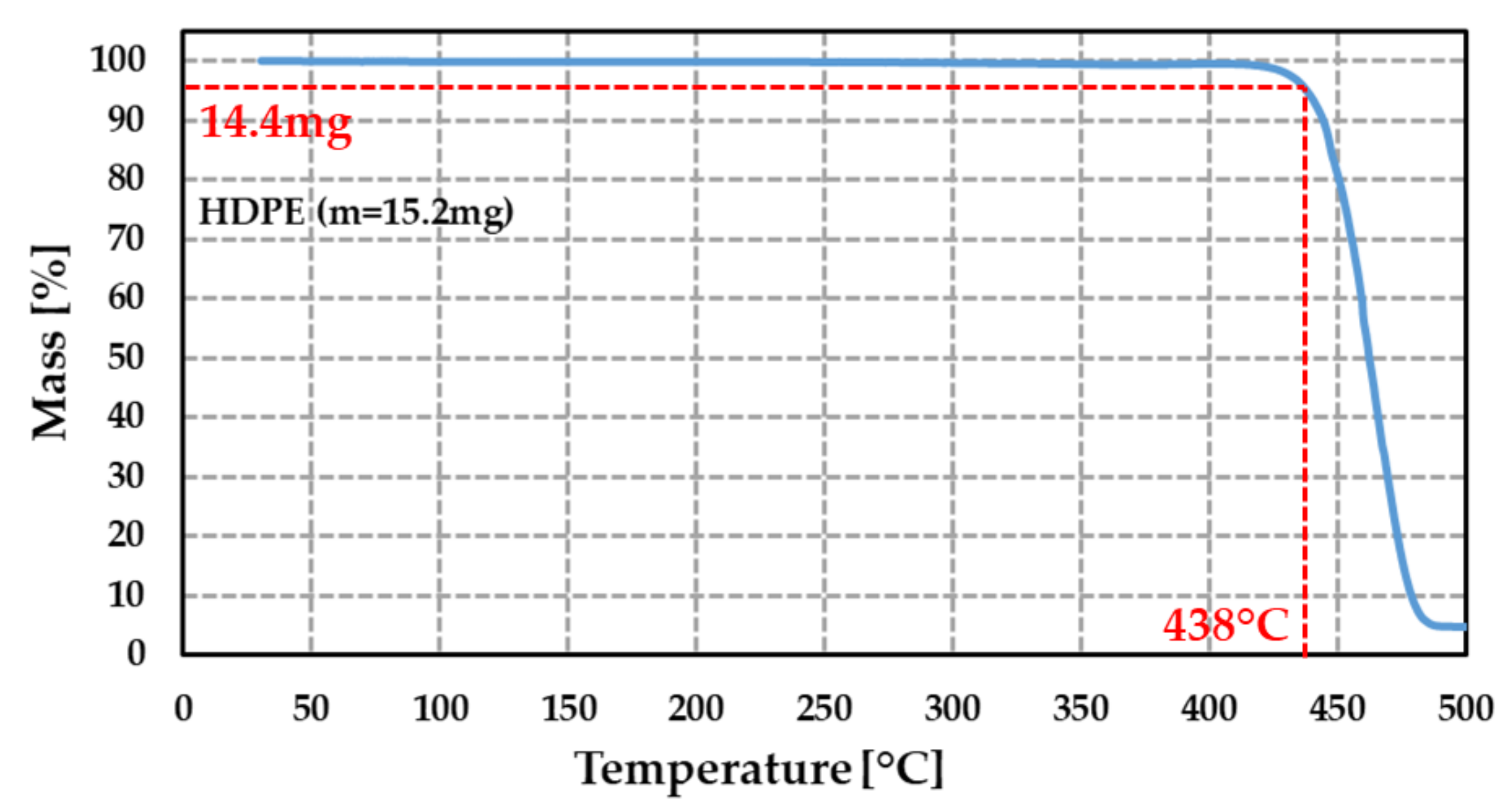
Figure 7.
Variation (in %) of the measured mass of HDPE sample as a function of the temperature (initial mass = 15.2 mg). Measurement was performed using a temperature ramp of 5 °C·min−1.
Figure 7.
Variation (in %) of the measured mass of HDPE sample as a function of the temperature (initial mass = 15.2 mg). Measurement was performed using a temperature ramp of 5 °C·min−1.
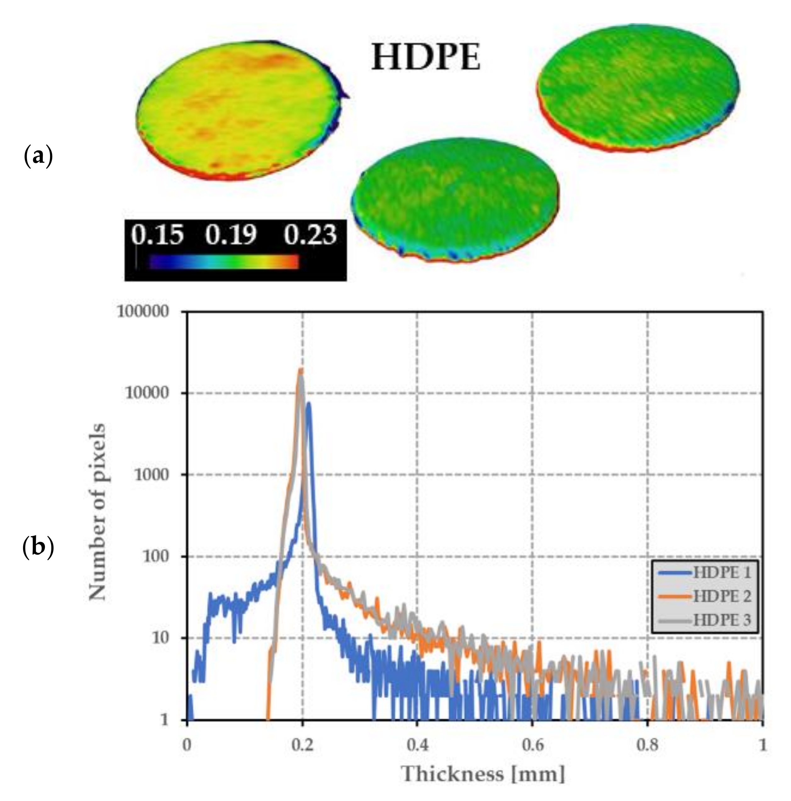
Figure 8.
(a) Thickness of 3 HDPE disks measured from tomography (color bar is in mm), and (b) the number of locations (pixels) on the 3 HDPE disks for which the HDPE thickness takes the values reported in the x-axis.
Figure 8.
(a) Thickness of 3 HDPE disks measured from tomography (color bar is in mm), and (b) the number of locations (pixels) on the 3 HDPE disks for which the HDPE thickness takes the values reported in the x-axis.
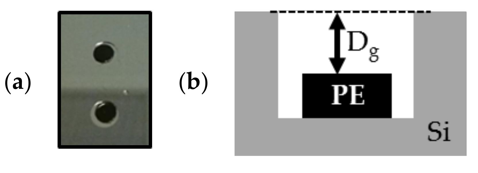
Figure 9.
(a) Photograph of PE samples (in black) placed in the cavity etched in silicon before annealing; (b) schematic of the cross-section of PE sample with the gap length between the top of the PE sample and the top of the cavity.
Figure 9.
(a) Photograph of PE samples (in black) placed in the cavity etched in silicon before annealing; (b) schematic of the cross-section of PE sample with the gap length between the top of the PE sample and the top of the cavity.
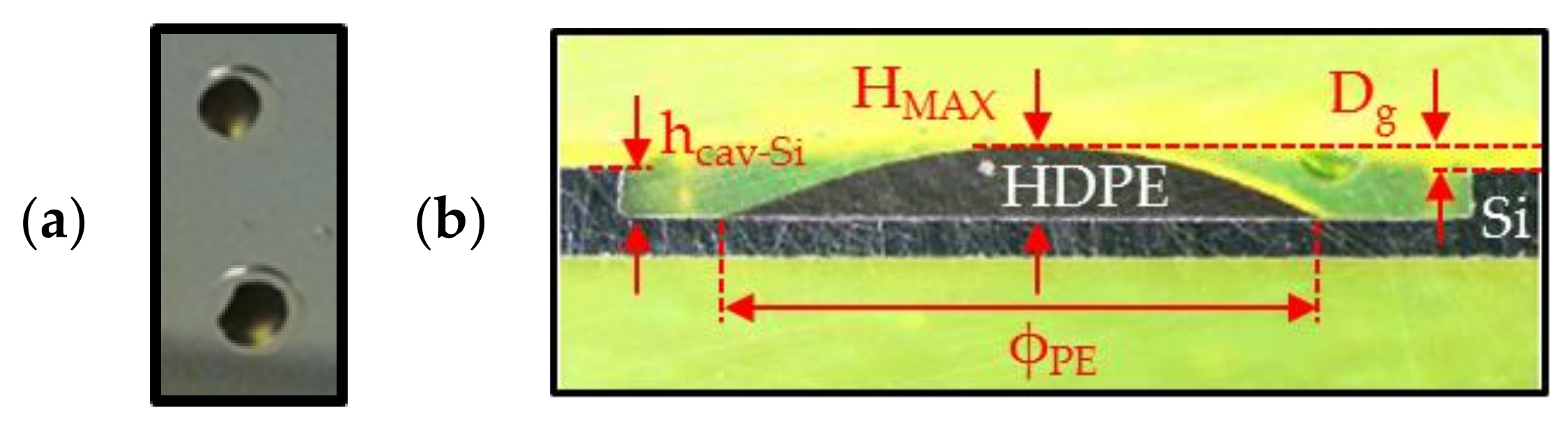
Figure 10.
(a) Photograph of PE samples (in black) placed in the cavity etched in silicon after annealing; (b) microsection photographs of a HDPE sample inside glass and silicon cavities.
Figure 10.
(a) Photograph of PE samples (in black) placed in the cavity etched in silicon after annealing; (b) microsection photographs of a HDPE sample inside glass and silicon cavities.
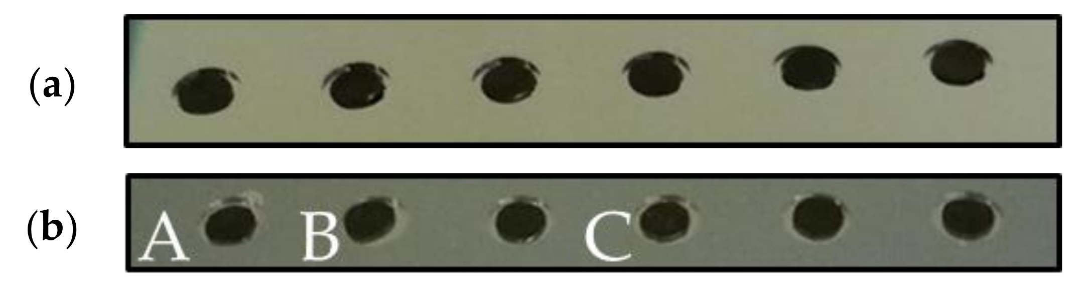
Figure 11.
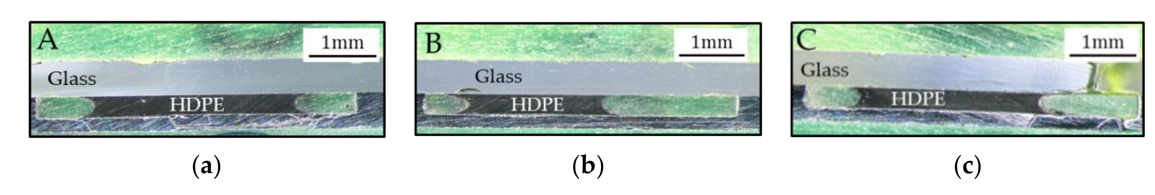
Photographs of the cavities filled with PE samples (
a) before and (
b) after annealing and anodic bonding. The microsection of cavities A, B and C are given in
Figure 12.
Figure 11.
Photographs of the cavities filled with PE samples (
a) before and (
b) after annealing and anodic bonding. The microsection of cavities A, B and C are given in
Figure 12.
Figure 12.
Photographs of the microsection after anodic bonding of the cavities A (
a), B (
b) and C (
c) filled with HDPE samples (see
Figure 11).
Figure 12.
Photographs of the microsection after anodic bonding of the cavities A (
a), B (
b) and C (
c) filled with HDPE samples (see
Figure 11).
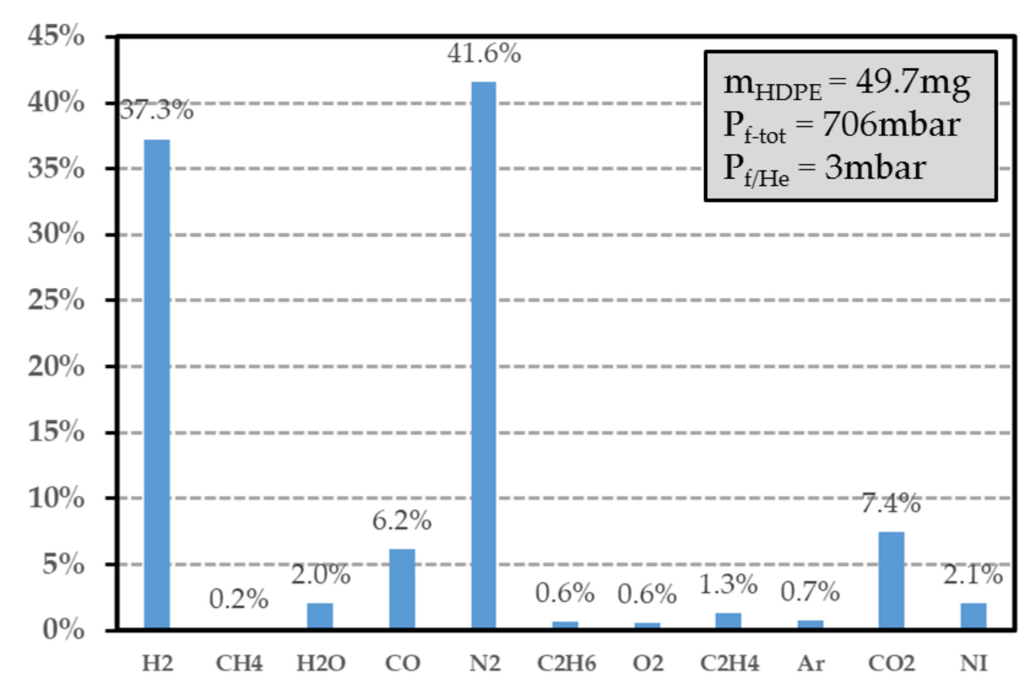
Figure 13.
Gas composition of the HDPE sample exposed at a dose level of 24.03 kGy (helium is removed from the spectrogram). The data in the ordinate (in %) represent the volume proportion of each detected gas. NI represents the species that are not identified. denotes the pressure after irradiation inside the vial, while is the final pressure without the helium contribution.
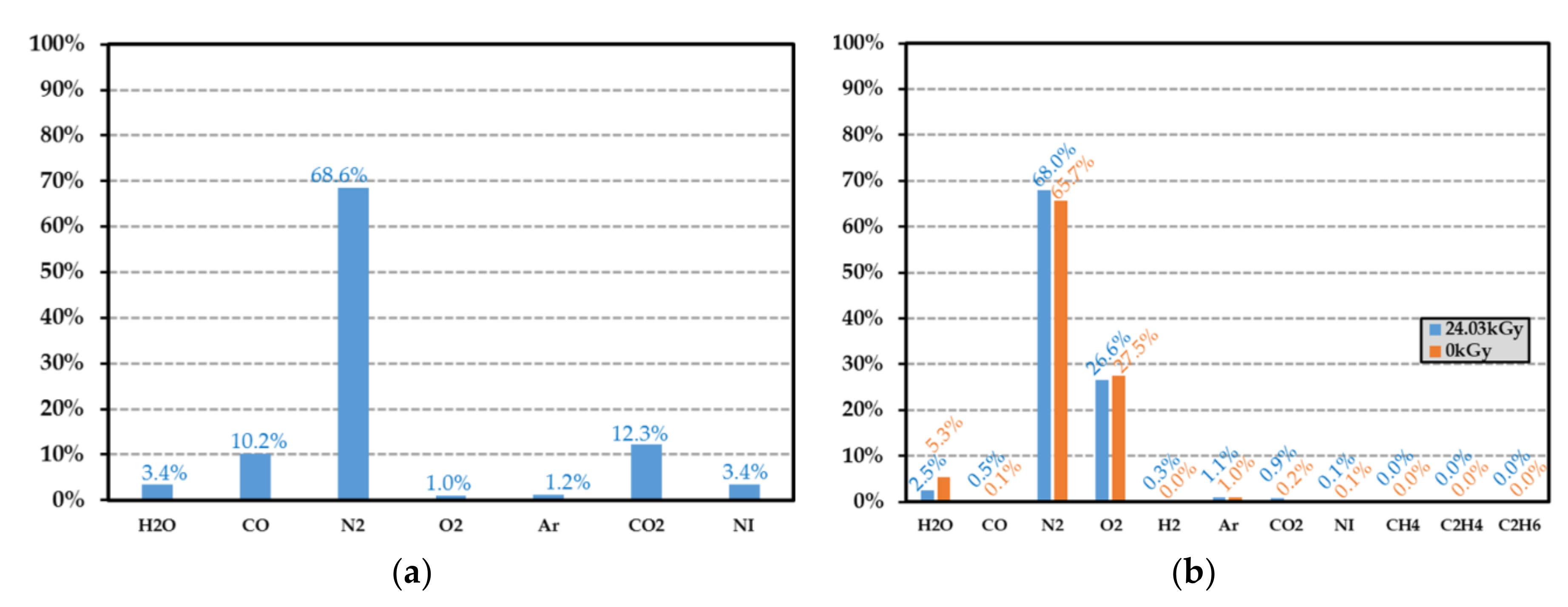
Figure 14.
(a) Gas composition after a 24.03 kGy dose exposure of a HDPE sample without the hydrogen contribution, and (b) gas composition of an empty test vial without polymer before and after an irradiation of 24.03 kGy. The helium contribution is not reported. In subfigure a, the volume proportions of dihydrogen and hydrocarbon molecules are not given. The data in the ordinate (in %) represent the volume proportion of each detected gases.
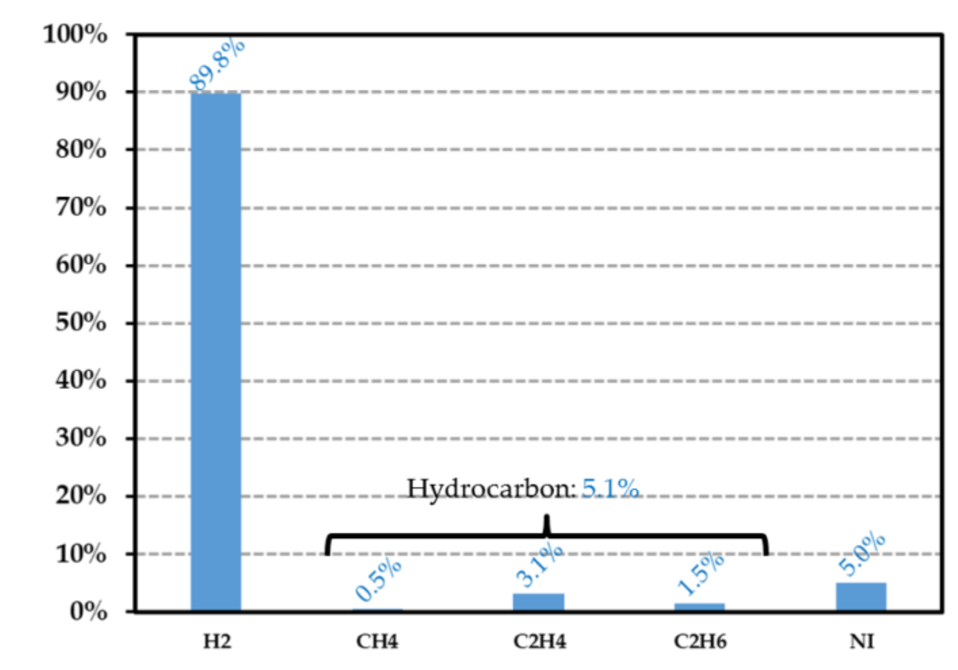
Figure 15.
Gas composition after irradiation of a 24.03 kGy HDPE sample. Proportions of , and are not reported. The data in the ordinate (in %) represents the volume proportion of each detected gases.
Figure 15.
Gas composition after irradiation of a 24.03 kGy HDPE sample. Proportions of , and are not reported. The data in the ordinate (in %) represents the volume proportion of each detected gases.
Figure 16.
Dimensions of the dosimeter: (
a) cross sectional view and (
b) photographs of the cavity fabricated on the glass substrate after anodic bonding [
9].
Figure 16.
Dimensions of the dosimeter: (
a) cross sectional view and (
b) photographs of the cavity fabricated on the glass substrate after anodic bonding [
9].
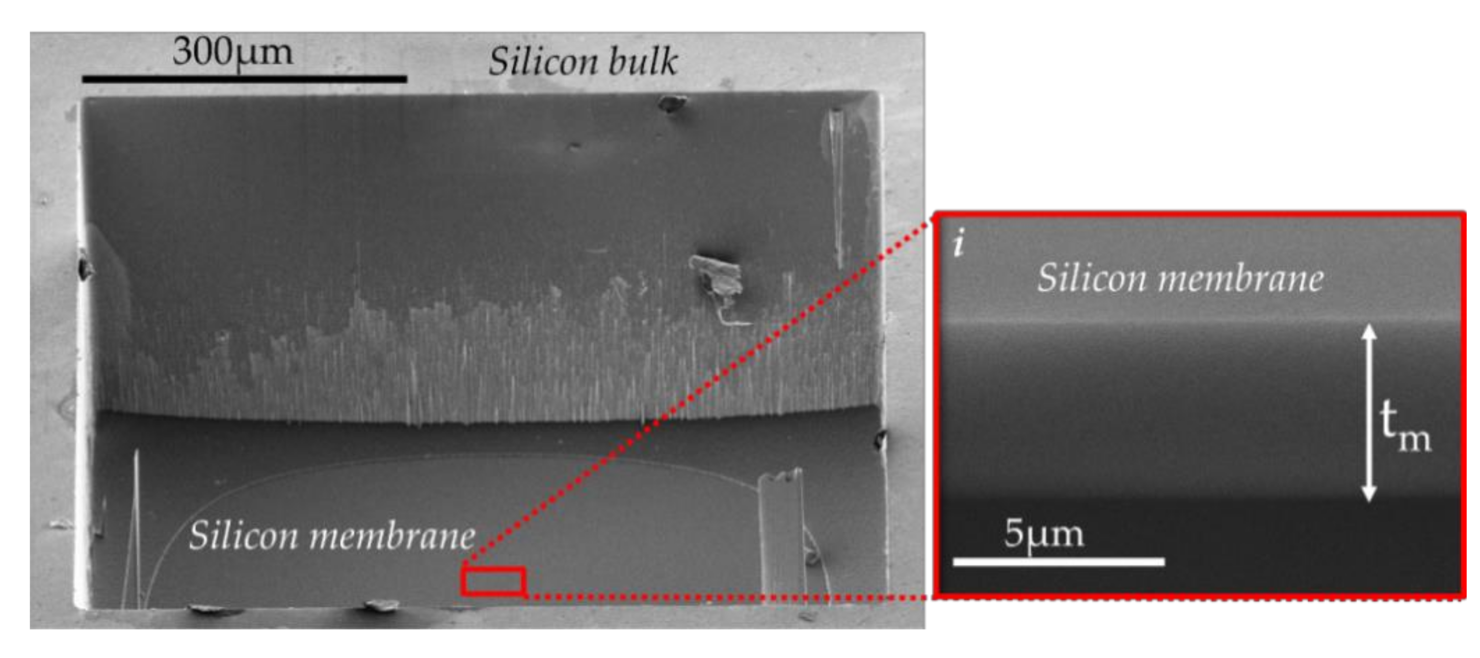
Figure 17.
SEM micrograph of the cavity membrane and FIB micrograph showing the membrane cross section (in inset i). denotes the thickness of the silicon membrane.
Figure 17.
SEM micrograph of the cavity membrane and FIB micrograph showing the membrane cross section (in inset i). denotes the thickness of the silicon membrane.
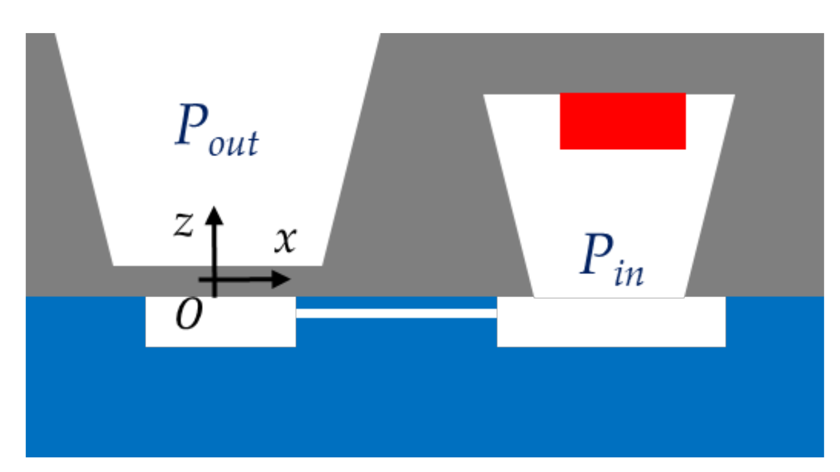
Figure 18.
Cross-sectional view of the dosimeter. The deflection amplitude is negative when the pressure inside the sealed cavity is lower than the pressure outside the cavity.
Figure 18.
Cross-sectional view of the dosimeter. The deflection amplitude is negative when the pressure inside the sealed cavity is lower than the pressure outside the cavity.
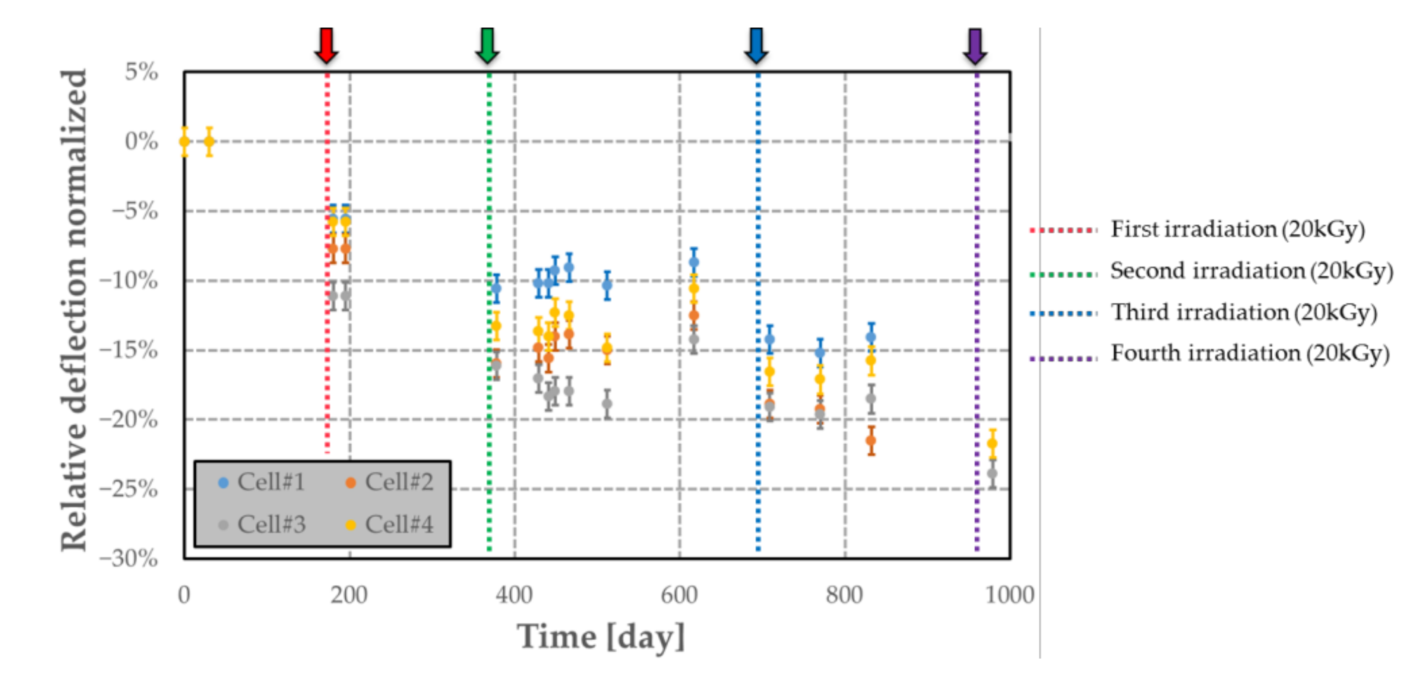
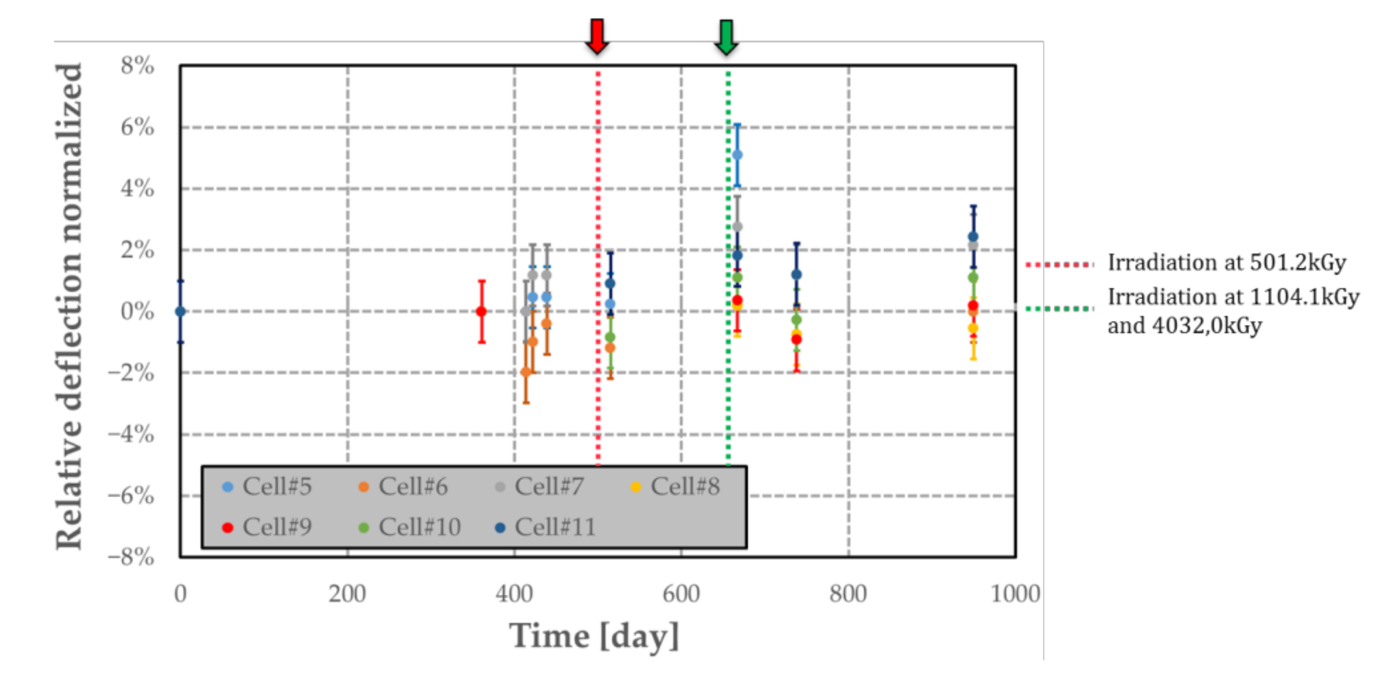
Figure 19.
Airtightness variation over time of passive MEMS transducers (with its polymer) subjected to several nuclear radiations. Each arrow indicates when the irradiation occurs (t = 0 refers to the time of the first deflection measurement).
Figure 19.
Airtightness variation over time of passive MEMS transducers (with its polymer) subjected to several nuclear radiations. Each arrow indicates when the irradiation occurs (t = 0 refers to the time of the first deflection measurement).
Figure 20.
Airtightness variation over time of MEMS transducers (without polymer) subjected to high dose levels. Each arrow indicates when the irradiation occurs (t = 0 refers to the time of the first deflection measurement).
Figure 20.
Airtightness variation over time of MEMS transducers (without polymer) subjected to high dose levels. Each arrow indicates when the irradiation occurs (t = 0 refers to the time of the first deflection measurement).
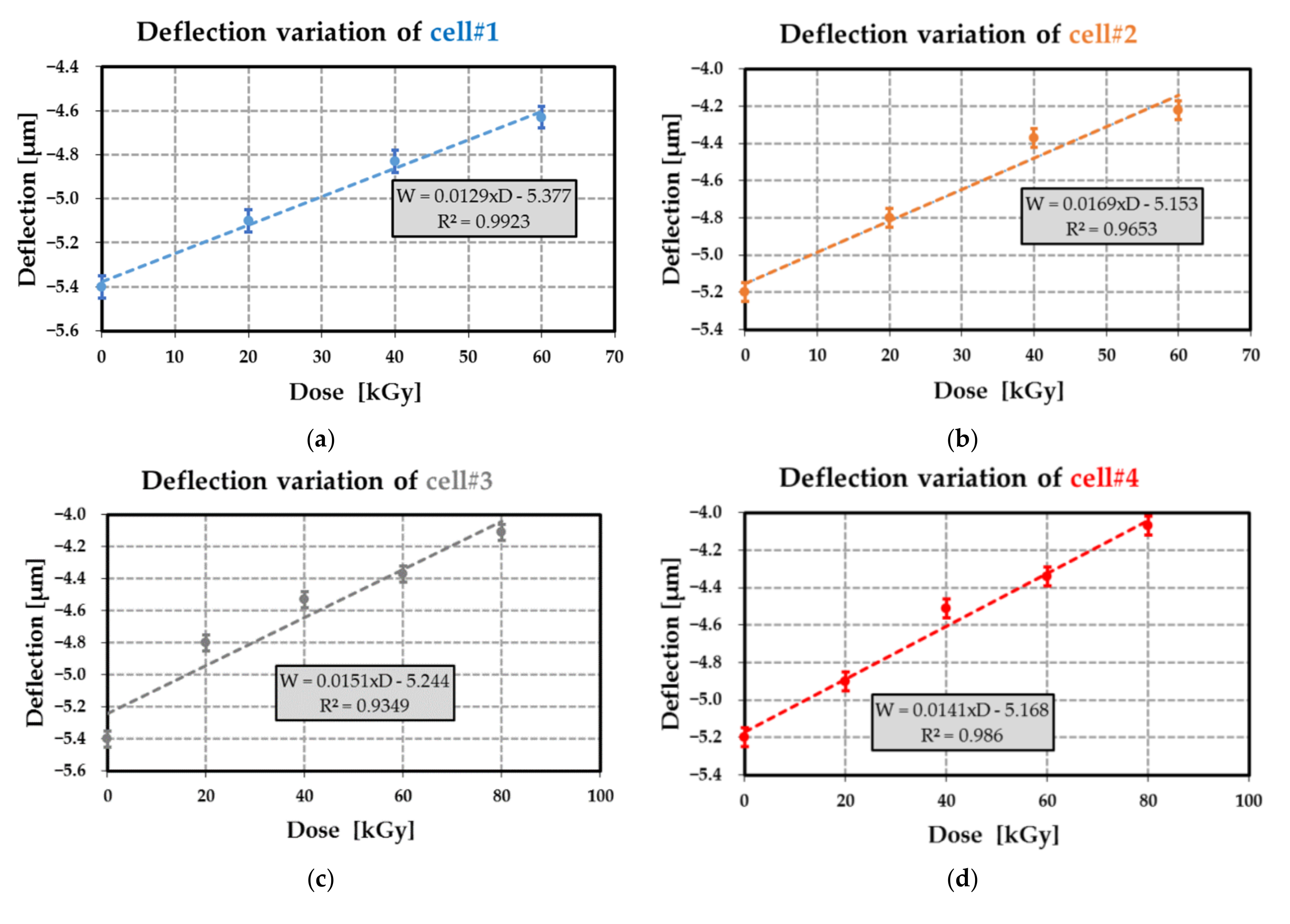
Figure 21.
Deflection as a function of the dose level for different passive MEMS test devices ((a) for cell#1; (b) for cell#2; (c) for cell#3 and (d) for cell#4). For each transducer the linear regression between the deflection W and the dose level D are reported (R2 designates the coefficient of determination of the linear regression).
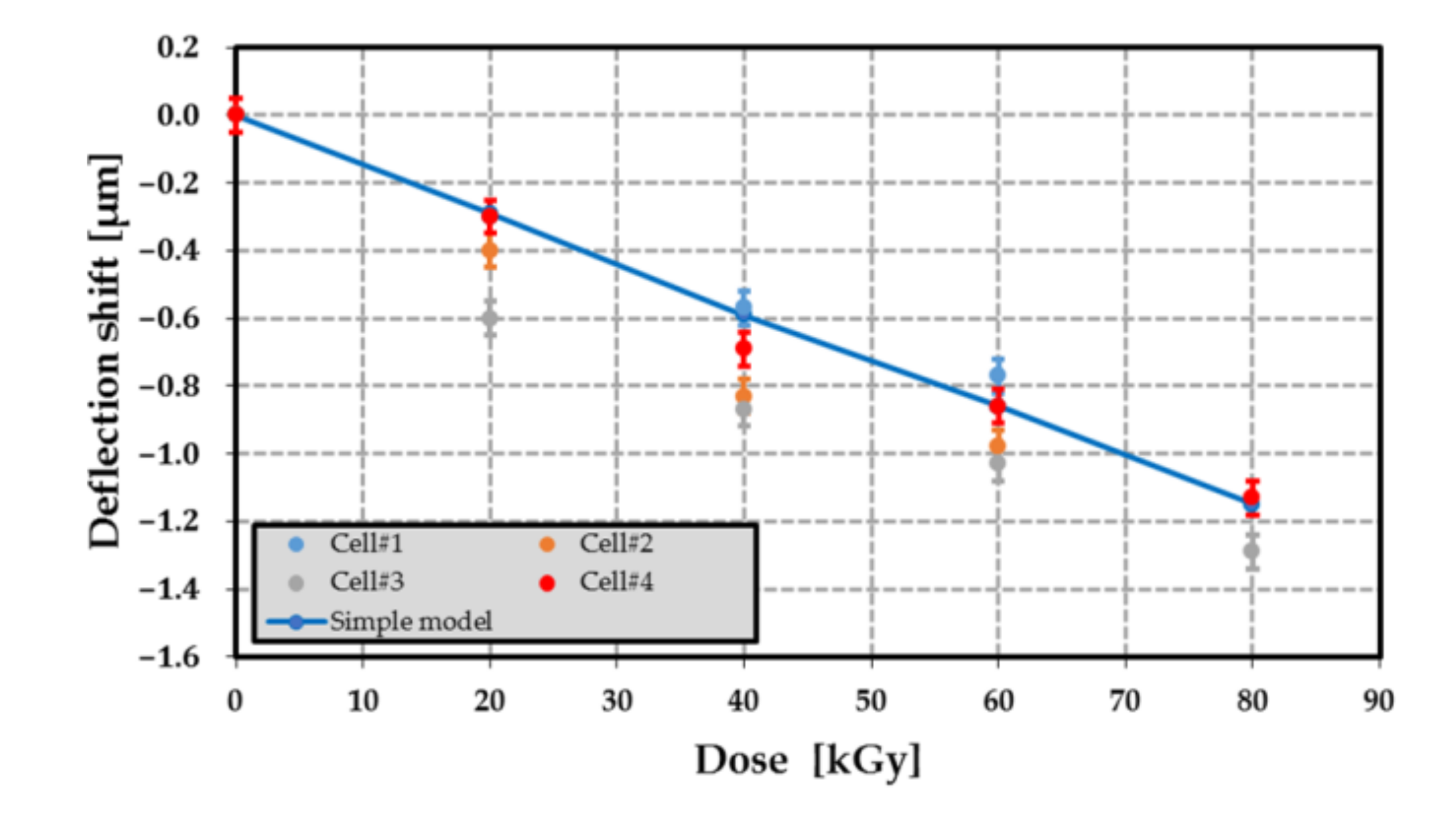
Figure 22.
Shift of the deflection as a function of the dose level for different passive MEMS transducers (cell#1 to #4). The blue line refers to the shift computed from the model of Equation (7).
Figure 22.
Shift of the deflection as a function of the dose level for different passive MEMS transducers (cell#1 to #4). The blue line refers to the shift computed from the model of Equation (7).
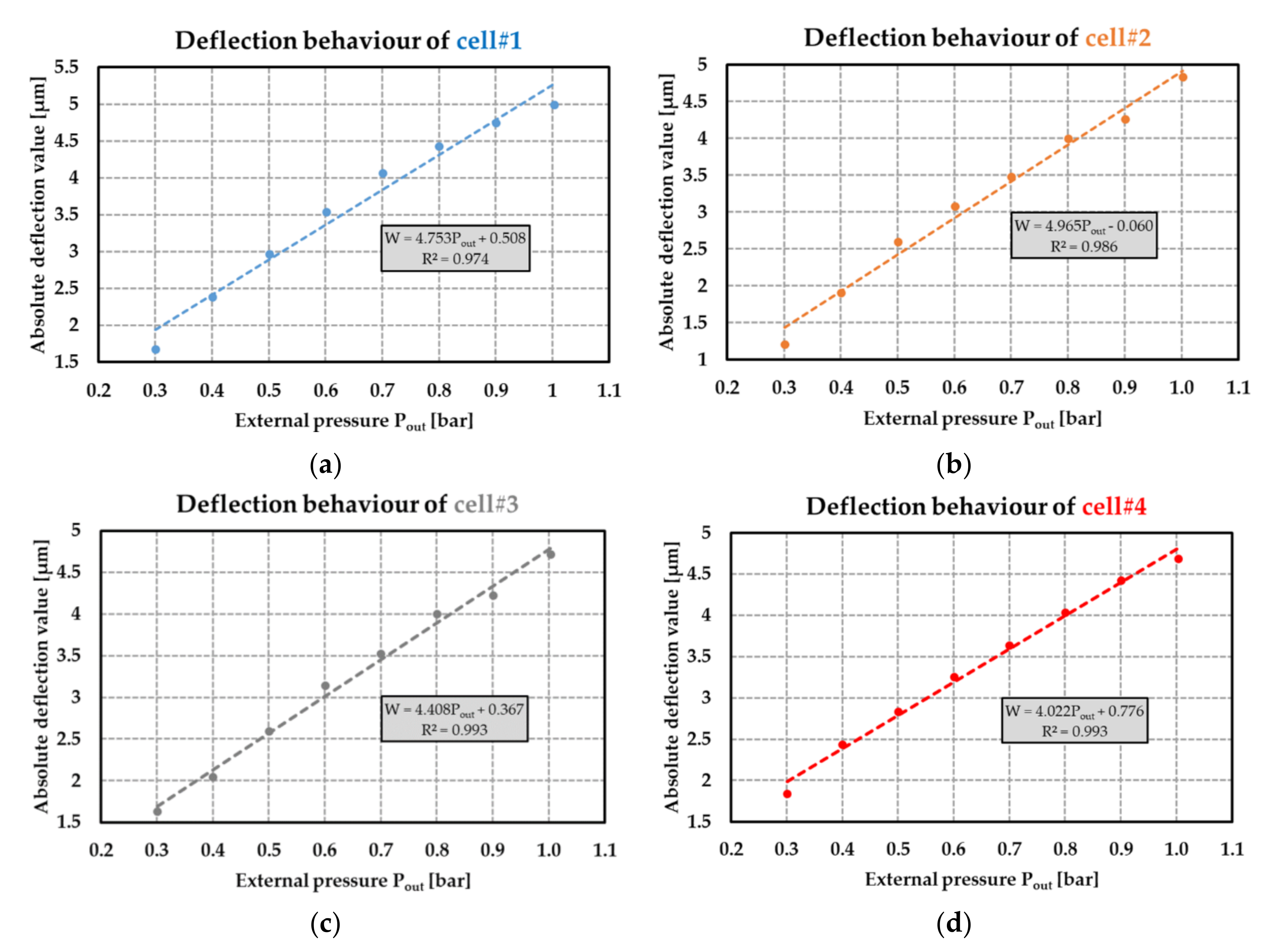
Figure 23.
Absolute value of the deflection with respect to the external pressure applied on the MEMS transducers: (a) for cell#1; (b) for cell#2; (c) for cell#3; and (d) for cell#4 (R2 denotes the coefficient of determination of the linear regression).
Figure 23.
Absolute value of the deflection with respect to the external pressure applied on the MEMS transducers: (a) for cell#1; (b) for cell#2; (c) for cell#3; and (d) for cell#4 (R2 denotes the coefficient of determination of the linear regression).
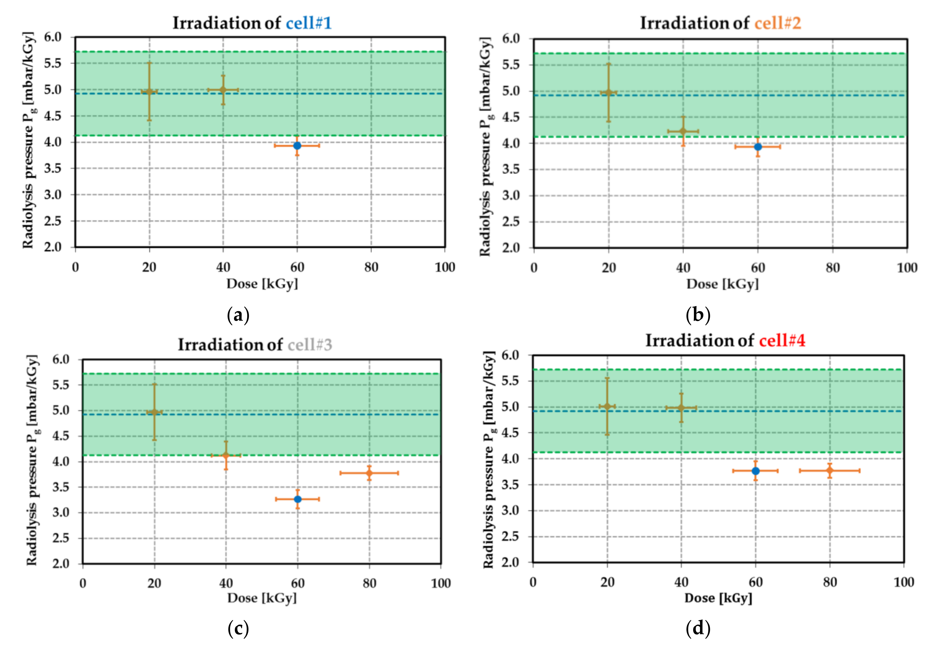
Figure 24.
Pressure
generated by the radiolysis as a function of the dose level (in kGy) for each MEMS transducers: (
a) for cell#1; (
b) for cell#2; (
c) for cell#3 and (
d) for cell#4. The blue point at 60 kGy is estimated from using the results of
Figure 23. The horizontal error bars refer to the 10% uncertainty on the dose level (see
Table 8), while the vertical error bars correspond to the uncertainty
δP on the pressure (see (26)). In the green region, the central dashed blue line and dashed green lines correspond respectively to the theoretical value of
at 4.92 mbar·kGy
−1 and the uncertainty
of ±0.80 mbar·kGy
−1 (see
Table 17) for the total gas emission yield factor
G of 4.4 × 10
−7 mol·J
−1 (see
Table 6).
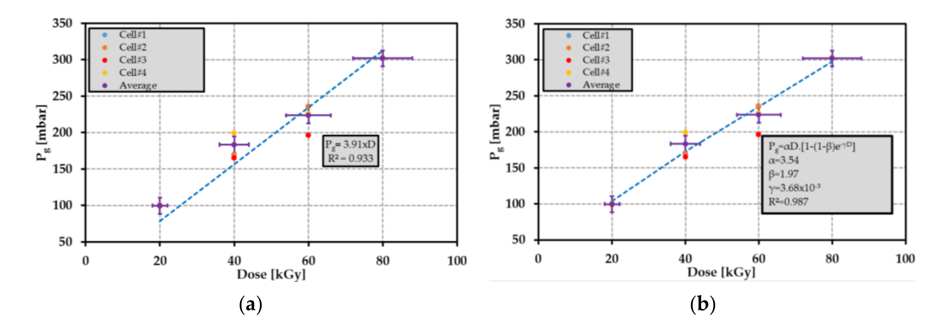
Figure 25.
Average pressure
(in magenta) as a function of dose level using (
a) a linear relationship and (
b) the exponential relationship proposed in [
95]. The blue, orange, red and yellow points refer to the radiolysis pressure for the cells #1; #2; #3 and #4, respectively.
Figure 25.
Average pressure
(in magenta) as a function of dose level using (
a) a linear relationship and (
b) the exponential relationship proposed in [
95]. The blue, orange, red and yellow points refer to the radiolysis pressure for the cells #1; #2; #3 and #4, respectively.
Table 1.
Height (in µm), diameter (in µm) and volume (in mm
3) of cavities patterned on the glass substrate (see
Figure 4).
Wch (in µm) and
Lch (in µm) denote, respectively, the width and length of the channel between the two cavities.
Table 1.
Height (in µm), diameter (in µm) and volume (in mm
3) of cavities patterned on the glass substrate (see
Figure 4).
Wch (in µm) and
Lch (in µm) denote, respectively, the width and length of the channel between the two cavities.
| hcav-glass | ϕcav1-glass | Lch | Wch | ϕcav2-glass | Vcav1-glass | Vch | Vcav2-glass | Vcav-glass |
|---|
| 10 | 550 | 2000 | 50 | 6000 | 2.38 × 10⁻³ | 1 × 10⁻³ | 2.83 × 10⁻¹ | 2.86 × 10⁻¹ |
Table 2.
Height (in µm), diameter (in µm) and volume (in mm3) of the cavity patterned on the silicon substrate, and the ratio ratios for HDPE samples of 3.5 mm diameter with two different thicknesses of 10 µm and 200 µm.
Table 2.
Height (in µm), diameter (in µm) and volume (in mm3) of the cavity patterned on the silicon substrate, and the ratio ratios for HDPE samples of 3.5 mm diameter with two different thicknesses of 10 µm and 200 µm.
| ϕcav-Si | | hcav-Si | VPO | Vcav-Si | Vg | VPO/Vg |
|---|
| 5000 | 10 | 60 | 9.62 × 10⁻² | 1.18 | 1.37 | 7.02% |
| 200 | 250 | 1.92 | 4.91 | 3.27 | 58.7% |
Table 3.
Mean thickness values for three different HDPE disks.
Table 3.
Mean thickness values for three different HDPE disks.
| Polymer | Mean Thickness Value (mm) | Mean Total Value (mm) | Standard Deviation (%) |
|---|
| HDPE #1 | 0.2108 | 0.201 | 4.2% |
| HDPE #2 | 0.1954 |
| HDPE #3 | 0.1973 |
Table 4.
Gap length between the top of the PE sample and the top of the cavity, and maximum thickness of PE sample inside the cavity after the annealing process. is the maximum thickness variation of the PE sample before and after annealing, while is the diameter of the PE sample after annealing.
Table 4.
Gap length between the top of the PE sample and the top of the cavity, and maximum thickness of PE sample inside the cavity after the annealing process. is the maximum thickness variation of the PE sample before and after annealing, while is the diameter of the PE sample after annealing.
| Polymer | ΦPE (mm) | hcav-Si (µm) | HMAX (µm) | Dg (µm) | ΔHMAX (µm) |
|---|
| HDPE#1 | 3.5 | 287 | 470 | 183 | 269 |
| HDPE#2 | 3.8 | 293 | 424 | 131 | 223 |
Table 5.
Typical gas composition in ambient environment.
Table 5.
Typical gas composition in ambient environment.
| N2 | O2 | Ar | H2O |
|---|
| 78.1% | 21.0% | 0.9% | Between 0.5% and 5% * |
Table 6.
Emission yield factors (in 10−7 mol·J−1) of each gas constituent after irradiation of an HDPE sample of 49.7 mg. The factor (in 10−7 mol·J−1) is the total emission yield factor and was calculated from summation of the emission yield factors of all gas constituents. DL stands for “quantity smaller than the Detection Limit of the apparatus” and NI stands for “Not Identified species”.
| PE Material | GH2 | GCH4 | GC2H4 | GC2H6 | NI | Ggas |
|---|
| HDPE (24.03 kGy irradiation) | 4.0 | <DL | 0.1 | 0.1 | 0.2 | 4.4 |
Table 7.
Hydrogen emission yield factor (in 10−7 mol·J−1) for different HDPE samples irradiated at two different dose levels and for various film thicknesses.
Table 7.
Hydrogen emission yield factor (in 10−7 mol·J−1) for different HDPE samples irradiated at two different dose levels and for various film thicknesses.
| Thickness and Sample Material | 12.15 kGy | 24.03 kGy |
|---|
| HDPE 10 µm thick | 4.1 | 4.3 |
| HDPE 200 µm thick | 3.9 | 4.0 |
| HDPE 1 mm thick | 3.7 | 4.1 |
Table 8.
Measurement uncertainties on the gas emission yield factors.
Table 8.
Measurement uncertainties on the gas emission yield factors.
| X | | Pf [mbar] | Vamp [cm3] | mPE [mg] | T [K] | D [kGy] | |
|---|
| | 1 | 0.27 | 0.1 | 1 | | |
| 1% | 0.14% | 2.7% | 0.22% | 0.33% | 10% | 10.4% |
Table 9.
Average value and standard deviations of 20 HDPE mass measurement results obtained by using a microbalance and performed on the same sample (reproducibility analysis).
Table 9.
Average value and standard deviations of 20 HDPE mass measurement results obtained by using a microbalance and performed on the same sample (reproducibility analysis).
| Average Value (mg) | Absolute Standard Deviation
(Δm, in mg) | Relative Standard Deviation
(Δm/m, in %) |
|---|
| 1.77 | 0.04 | 2.3 |
Table 10.
Average value and standard deviations of 35 mass measurement results obtained by using a microbalance (variability analysis).
Table 10.
Average value and standard deviations of 35 mass measurement results obtained by using a microbalance (variability analysis).
| Average Value (mg) | Absolute Standard Deviation
(Δm, in mg) | Relative Standard Deviation
(Δm/m, in %) |
|---|
| 1.78 | 0.09 | 5.1 |
Table 11.
Average and standard deviation of measured height of cavities etched into the glass substrate.
Table 11.
Average and standard deviation of measured height of cavities etched into the glass substrate.
| # Substrate | 1 | 2 | 3 | 4 | Overall Average |
|---|
| ĥcav-glass [µm] | 8.890 | 8.952 | 8.730 | 8.870 | 8.859 |
| Δhcav-glass [µm] | 0.090 | 0.079 | 0.097 | 0.089 | 0.089 |
| Δhcav-glass/hcav-glass | | | | | 1.0% |
Table 12.
Relative and absolute uncertainties on the cavity volume performed on the glass substrate.
Table 12.
Relative and absolute uncertainties on the cavity volume performed on the glass substrate.
| hcav-glass [µm] | | | Vcav2-glass [mm3] | ΔVcav2-glass [mm3] | |
|---|
| 10 | 6016.21 | 2.13 | 2.827 × 10⁻¹ | 2.530 × 10⁻³ | 0.9 |
Table 13.
Average and standard deviation of measured height of cavities etched into the silicon substrate.
Table 13.
Average and standard deviation of measured height of cavities etched into the silicon substrate.
| # Substrate | 1 | 2 | 3 | 4 | Overall Average |
|---|
| ĥcav-Si [µm] | 290.50 | 320.22 | 310.80 | 304.60 | 304.28 |
| Δhcav-Si [µm] | 1.29 | 2.84 | 2.64 | 1.34 | 2.02 |
| Δhcav-Si/hcav-Si | | | | | 0.7% |
Table 14.
Relative and absolute uncertainties on the cavity volume performed on the silicon substrate.
Table 14.
Relative and absolute uncertainties on the cavity volume performed on the silicon substrate.
| hcav-Si [µm] | | | Vcav-Si [mm3] | ΔVcav-Si [mm3] | |
|---|
| 290 | 5000 | 2 | 5.694 | 3.986 × 10⁻² | 0.7 |
Table 15.
Relative and absolute uncertainties on the sealed cavity volume Vg.
Table 15.
Relative and absolute uncertainties on the sealed cavity volume Vg.
| Vg [mm3] | ΔVg [mm3] | |
|---|
| 4.044 | 0.214 | 5.3 |
Table 16.
Relative uncertainties ΔX/X on the parameter X appearing in (16).
Table 16.
Relative uncertainties ΔX/X on the parameter X appearing in (16).
| X | | mPE | | T | D | |
|---|
| ΔX/X | 10.4% | 5.1% | 5.3% | 0.3% | 10.0% | 16.2% |
Table 17.
Theoretical determination of the pressure generated by polymer radiolysis during nuclear irradiation and membrane deflection for five different dose levels. denotes the absolute uncertainty on pressure .
Table 17.
Theoretical determination of the pressure generated by polymer radiolysis during nuclear irradiation and membrane deflection for five different dose levels. denotes the absolute uncertainty on pressure .
| Dose Level [kGy] | Pg [mbar] | ΔPg [mbar] | ΔWg [µm] |
|---|
| 1 | 4.92 | 0.80 | 0.01 |
| 20 | 98.44 | 15.95 | 0.29 |
| 40 | 196.88 | 31.89 | 0.57 |
| 60 | 295.32 | 47.84 | 0.86 |
| 80 | 393.76 | 63.79 | 1.15 |
Table 18.
Composition, partial pressure (in mbar) inside (noted in.) and outside (noted out.) of the cavity and permeation coefficient (in cm2·s−1) through silicon () and glass () for some components X at a given temperature. corresponds to the difference of partial pressure (in mbar) for each gas component inside and outside the cavity.
| Gas Component | Gas Composition (out.) | Partial Pressure (out.) | Gas Composition (in.) | Partial Presssure (in.) | | | |
|---|
| 78.1% | 781 | 0% | 0 | 781 | 5.0 × 10⁻¹⁷ (25 °C) | <1.9 × 10⁻¹¹ (1200 °C) |
| 21.0% | 210 | 0% | 0 | 210 | 5.0 × 10⁻¹⁷ (25 °C) | NR |
| 0.9% | 9 | 0% | 0 | 9 | <10−15 (700 °C) | <1.9 × 10⁻¹¹ (1200 °C) |
| 4.2 × 10⁻²% | 4.2 × 10⁻¹ | 0% | 0% | 4.2 × 10⁻¹ | NR | NR |
| 0.5–5% | 5–50 | 0% | 0 | 5–50 | NR | NR |
| 1.8 × 10⁻⁴% * | 1.8 × 10⁻³ * | 5.1% * | 5.1 * | 5.1 * | NR | NR |
| 5.5 × 10⁻⁵% | 5.5 × 10⁻⁴ | 89.8% | 898.0 | 898 | 3.4 × 10⁻¹⁶ (20 °C) | 5.7 × 10−40 (20 °C) |
| 5.2 × 10⁻⁴% | 5.2 × 10⁻³ | 0% | 0 | 5.2 × 10⁻³ | 3.5 × 10⁻¹¹ (20 °C) | 3.2 × 10⁻³⁴ (20 °C) |
| 1.8 × 10⁻³% | 1.8 × 10⁻² | 0% | 0 | 1.8 × 10⁻² | 2 × 10⁻¹⁶ (25 °C) | <1.9 × 10⁻¹¹ (1200 °C) |
| 1.1 × 10⁻⁴% | 1.1 × 10⁻³ | 0% | 0 | 1.1 × 10⁻³ | NR | NR |
Table 19.
Diffusion coefficient at room temperature noted
Droom for some chemical species in amorphous silicon dioxide [
102].
Table 19.
Diffusion coefficient at room temperature noted
Droom for some chemical species in amorphous silicon dioxide [
102].
| Molecule | Droom [cm2·s−1] |
|---|
| 2.8 × 10⁻⁸ |
| 1.5 × 10⁻¹¹ |
| 5.3 × 10⁻²⁰ |
Table 20.
Partial pressure difference, permeation rate through the glass material and leak rate for each gas component.
Table 20.
Partial pressure difference, permeation rate through the glass material and leak rate for each gas component.
| Gas Component | | | |
|---|
| 781 | 5.0 × 10⁻¹⁷ (25 °C) | 8.8 × 10⁻¹⁶ |
| 210 | 5.0 × 10⁻¹⁷ (25 °C) | 2.4 × 10⁻¹⁶ |
| 898 | 3.4 × 10⁻¹⁶ (20 °C) | 6.9 × 10⁻¹⁵ |
Table 21.
Time (in years) necessary to see a difference inside the cavity.
Table 21.
Time (in years) necessary to see a difference inside the cavity.
| Gas Component | | | | |
|---|
| ~7600 | ~1470 | ~730 | ~150 |
| ~30,620 | ~5500 | ~2710 | ~540 |
| ~960 | ~190 | ~94 | ~19 |


 ,
, 


