
Novel Bandwidth Expander Supported Power Amplifier for Wideband Ultrasound Transducer Devices

Department of Medical IT Convergence Engineering, Kumoh National Institute of Technology, 350-27 Gumi-daero, Gumi 39253, Korea
*
Author to whom correspondence should be addressed.
Sensors 2021, 21(7), 2356; https://doi.org/10.3390/s21072356
Submission received: 17 February 2021
/
Revised: 24 March 2021
/
Accepted: 25 March 2021
/
Published: 28 March 2021
(This article belongs to the Special Issue Imaging Sensors and Applications)
Abstract
:Ultrasound transducer devices have their own frequency ranges, depending on the applications and specifications, due to penetration depth, sensitivity, and image resolution. For imaging applications, in particular, the transducer devices are preferable to have a wide bandwidth due to the specific information generated by the tissue or blood vessel structures. To support these ultrasound transducer devices, ultrasound power amplifier hardware with a wide bandwidth can improve the transducer performance. Therefore, we developed a new bandwidth expander circuit using specially designed switching architectures to increase the power amplifier bandwidth. The measured bandwidth of the power amplifier with the help of the bandwidth expander circuit increased by 56.9%. In addition, the measured echo bandwidths of the 15-, 20-, and 25-MHz transducer devices were increased by 8.1%, 6.0%, and 9.8%, respectively, with the help of the designed bandwidth expander circuit. Therefore, the designed architecture could help an ultrasound system hardware with a wider bandwidth, thus supporting the use of different frequency ultrasound transducer devices with a single developed ultrasound system.
1. Introduction
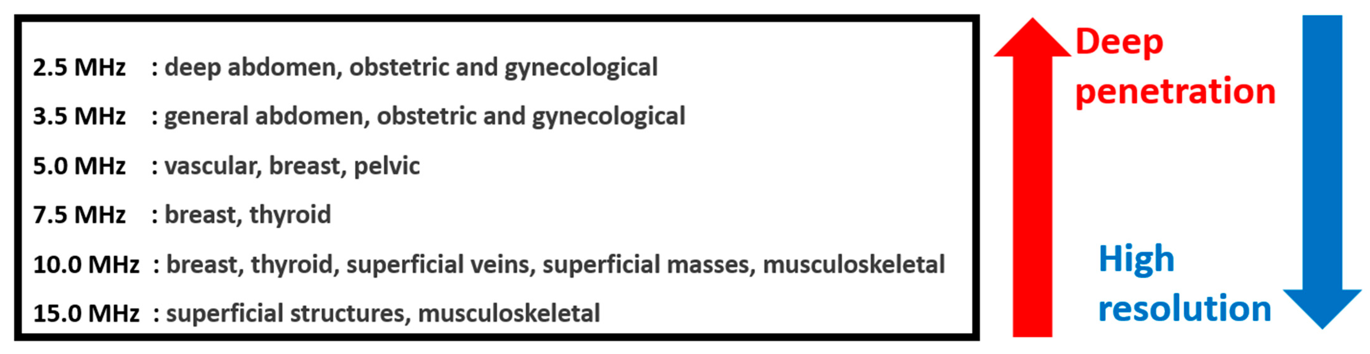
Ultrasound transducers are the main sensor devices used in ultrasound systems [1]. Different types of ultrasound transducers are used, depending on their applications and specifications [2]. Engineers have manufactured ultrasound transducers with the required diagnostic applications. For diagnostic applications with different positions and locations, the imaging resolution and sensitivity performance are merits in the evaluation of ultrasound systems [3]. Typically, lower-frequency ultrasound transducer devices have a higher penetration depth and lower imaging resolution than higher-frequency ultrasound transducer devices [4]. Smaller-sized ultrasound transducer devices for intracardiac and intravascular applications need to be used such that the penetration depth of the devices is lower, but a higher imaging resolution could be preferable [5].
Figure 1 shows the penetration depth and imaging resolution for an ultrasound diagnostic analysis. Since the imaging resolution and penetration depth have a trade-off relationship, ultrasound transducers with smaller piezoelectric elements are used depending on the body parts [6]. For the heart and abdomen areas, 2–3 and 3–5 MHz transducer devices are preferable because of the penetration depth [5,7]. For the eyeballs and breast and thyroid areas, 7.5–12 MHz and 7.5–13 MHz transducer devices are used due to their relatively high imaging resolutions [5,7]. In particular, for peripheral blood vessels and digestive tract areas, small transducer devices with a high frequency, such as 15–30 MHz, are used because of the higher imaging resolution, which reduces the penetration depth [8,9,10].
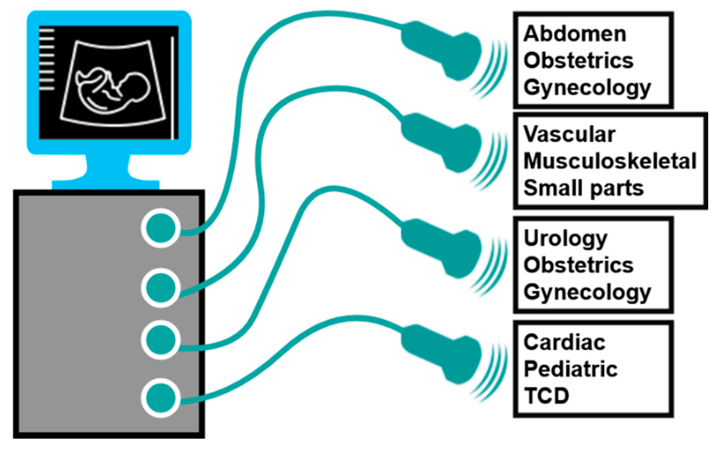
Figure 2 shows the ultrasound transducer probes (devices) used in ultrasound systems for specific applications [7,11]. Each ultrasound transducer probe has different frequency characteristics and shapes; thus, different anatomical cross-sectional images are obtained [11,12]. However, only one ultrasound system may not cover the transducer probes with different frequency ranges.
Various classes of power amplifiers have been developed for different types of ultrasound transducer devices. In power amplifiers, the input signals are amplified by active devices, which we call metal-oxide-semiconductor field-effect transistors (MOSFETs) or lateral-diffusion metal–oxide semiconductors (LDMOSs) [13]. Depending on the direct current (DC) bias voltages, the output currents generated by the active devices are fully or partially conducted during a single period of time [14]. This fundamental concept is used to categorize power amplifier classes, such as classes A, B, and C. In the Class A power amplifier, the operating bias voltage is located in the middle of the DC load line to minimize signal distortions [15]. Therefore, the active device in the power amplifier has a heavy load because the active device continues to operate regardless of the input signal [16,17]. Power is consumed continuously as long as an active device is operating. However, signal distortion by an active device is minimized, resulting in an output signal with high linearity [18]. In Class B power amplifiers, the bias voltage is located near the middle of the DC load line, and thus, the active device operates only for half the period of the signal [17]. Therefore, the active device operates for only half a period, which causes signal distortion, although the power consumption of the active device is reduced, compared to that of the Class A power amplifier. Class C power amplifiers operate for less than half a period of the signal because the bias voltage of the DC load line is lower than that of Class B amplifiers [13]. Therefore, the distortion of the signal is extremely high, whereas the power consumption of the active device is quite low. In addition, Class AB power amplifiers operate between Class A and B power amplifiers. In addition, there are other types of power amplifiers, such as Class D and Class E, which use harmonic components or modulated waveforms [19].
The Class B power amplifiers operate at only half of the pulse cycle, which has a much shorter time than Class A and Class AB power amplifiers. Therefore, Class B power amplifiers have much lower power consumption than those of Class A and Class AB power amplifiers, and thus, they have a higher efficiency [20]. The Class B power amplifier has lower signal distortions than the Class A power amplifier. Therefore, wire-type ultrasound machines have a Class A power amplifier because of the AC power cord [2]. Class B or Class C power amplifiers are preferable for mobile or portable ultrasound systems due to their limited battery modules [6]. Several studies related to power amplifiers have been conducted on ultrasound-transducer devices. For ultrasound signals, the burst or modulated waveforms with a limited time period and non-continuous signals are used. A typical Class A power amplifier was developed for ultrasound imaging applications [21]. A Class B power amplifier was developed to reduce the signal distortion [22].
There are a few studies of the power amplifiers used for ultrasound applications. There is a Class C power amplifier used for a 25 MHz transducer. This amplifier has high efficiency with high signal distortions. Therefore, the proposed circuit was developed to compensate for signal distortions [23]. Class D amplifier was developed for low-frequency piezoelectric transducers [24]. This amplifier was used for the high signal distortion and high-efficiency system. The Class E power amplifier was developed to improve the efficiency of low-frequency inductive piezoelectric converters [25]. As mentioned, various power amplifiers with various characteristics are used because all the amplifiers cannot satisfy some parameters of the signal distortion and the bandwidth. In ultrasound systems, transmitter and receiver architectures support ultrasound devices. The power amplifier in a transmitter is typically used in the last stage of electronics [2]. Thus, the bandwidth of the power amplifier only covers the specific transducer probes with their limited frequency ranges because the bandwidth of the power amplifier electronic devices decreases as the operating frequency of the power amplifier increases. This indicates that the output signals working at frequencies higher than the center frequency may deteriorate the image quality. Therefore, we first proposed a bandwidth-expander circuit for power amplifiers and various ultrasound devices.
There are several ways to increase the bandwidth of the power amplifier output. Impedance matching improves the amplitude and bandwidth of the power amplifiers and ultrasound transducers [26]. The output power can be increased through impedance matching, thus increasing the echo amplitude or the echo bandwidth of the ultrasound transducers [26]. However, the impedance of the ultrasound transducer varies significantly according to the frequency [27]. Furthermore, transducers are manufactured to have different central frequencies and resonance/anti-resonance frequency ranges [28]. Therefore, it can be difficult to match the impedance magnitudes within the desired frequency ranges for several ultrasound transducers.
Another method is to lower the gain and increase the bandwidth of the power amplifier by using a feedback loop circuit [14]. This method a fundamental approach for increasing the bandwidth of a power amplifier. This method can reduce the gain of the power amplifier and increase the bandwidth [16]. Thus, several-stage power amplifiers need to be utilized to increase the gain and bandwidth. As the number of stages increases, various problems such as a time delay and signal distortions due to line resistances and parasitic nonlinear components could affect the performance of the power amplifiers [29]. Moreover, there could be a bandwidth expansion limit because space and cost are finite in terms of manufacturing.
In this study, we developed a circuit that can enlarge the bandwidth and minimize the signal loss, thus applying it to a single-stage power amplifier. In our proposed circuit, the bandwidth can be improved by lowering the input poles of the power amplifiers. The designed circuit works as a switching mode that is simply turned on/off with DC power. This method can be useful to improve the bandwidth of the power amplifier and minimize the signal loss, thus supporting higher-frequency ultrasound devices. Section 2 describes the theoretical background and analysis of the proposed circuit and the power amplifier. Section 3 presents the measured performance and a discussion of the proposed circuit with several ultrasound transducers. Section 4 provides some concluding remarks regarding this research.
2. Materials and Methods
The designed bandwidth expander (BWE) is a type of switching circuit operated by different applied DCs. It is located before the lateral-diffusion metal-oxide-semiconductor field-effect transistor (PD57018-E, LDMOSFET, STMicroelec-tronics, Geneva, Switzerland), which is a type of high-voltage MOSFET (BSS123, active device in BWE) in the input port of the amplifier. When the active LDMOSFET device in the amplifier operates under higher-voltage amplitudes than a certain bias voltage, the amplifier is applied to the gate of the LDMOSFET [30]. Therefore, the drain and source of the MOSFET are applied such that the input impedance of the amplifier is changed accordingly. In addition, by adjusting the input impedance, the input poles of the amplifier can be tuned. The total transfer function of the amplifier is expected to increase by integrating the BWE circuit with the amplifier. Therefore, the amplifier with the help of the BWE has a higher output amplitude and wider bandwidth.
2.1. Designed Power Amplifier and BWE Schematic Diagram
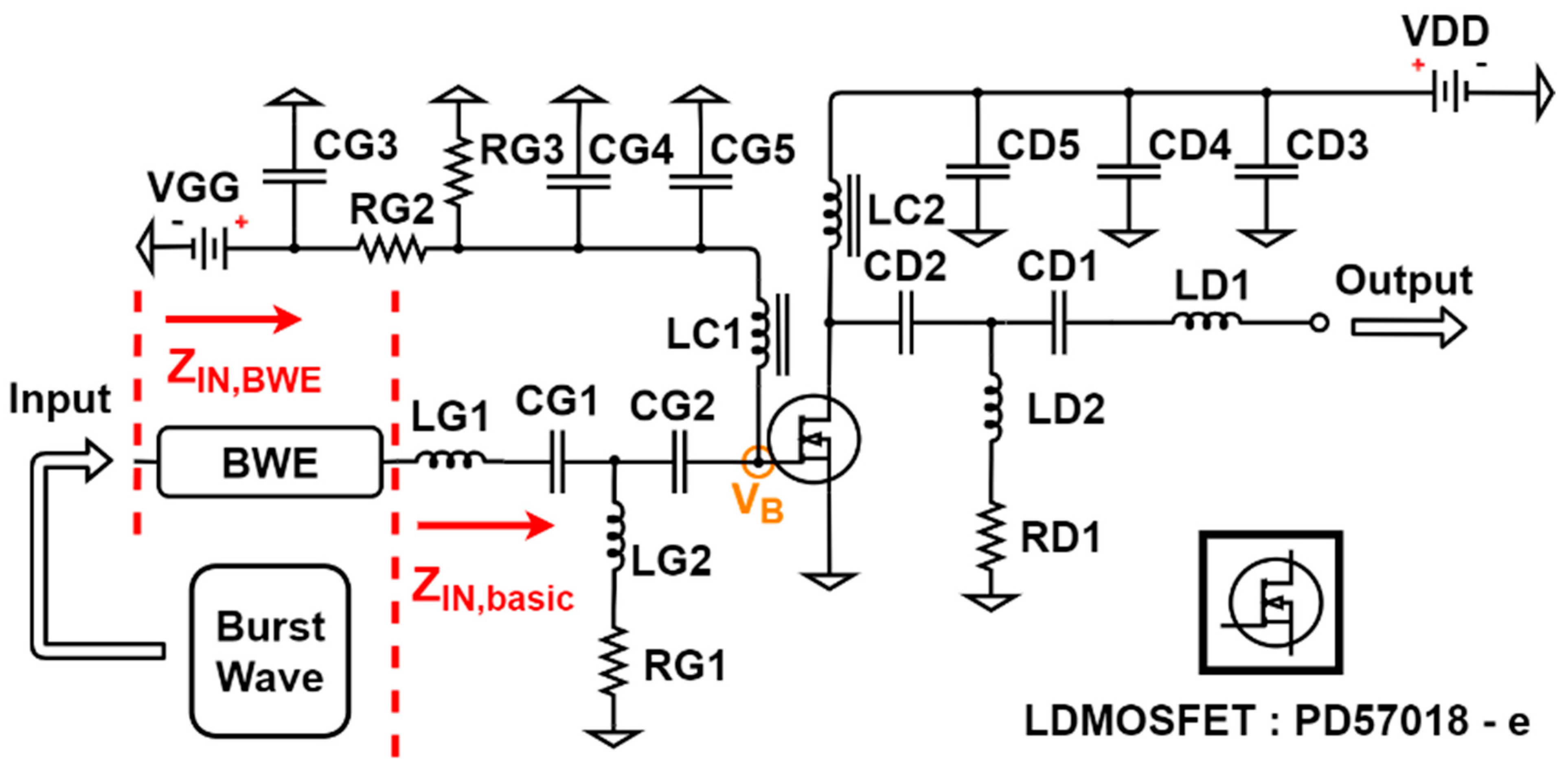
Figure 3 shows an amplifier combined with a BWE circuit for the ultrasound transmitter. Table 1 shows the resistor, capacitor, and inductor elements of the amplifier, except for the LDMOSFET shown in Figure 3. The LDMOSFET (PD57018-E, STMicroelectronics, Geneva, Switzerland) was used as the core component of the amplifier. The simulation was conducted to make the impedance matching suitable for the 15 MHz transducer. In Figure 3, VB is the main gate-source operating point of the LDMOSFET. In addition, LC1 and LC2 are choke coil inductors that prevent the inflow of the alternating current (AC) into the DC power supply [31]. The components used in the input line (LG1, LG2, CG1, CG2, and RG1) and the components used in the output line (LD1, LD2, CD1, CD2, and RD1) are tuned to be compatible with the 15 MHz transducer and to achieve the values below −10 dB of S (1,1) and S (2,2). In addition, they need to block the DC current from VGG and VDD using CG2 and CD2. If AC input voltages enter the DC power supply, oscillations may occur [32]. The polarizing electrolytic capacitors CG3 and CD2 are helpful in providing a constant direct voltage [33]. The ceramic capacitors CG4, CG5, CD4, and CD5 were used to reduce noise as bypass capacitors. The bias voltage was adjusted to operate through the voltage distributions of RG2 and RG3. The bias voltage equation at VB is as follows [34,35]:
In ultrasonic diagnostic equipment, the frequency of the input signal and the cycle of the burst wave were adjusted such that the Q factor used for providing an appropriate image quality was calculated [1]. Assuming that the LDMOSFET operates in the saturation region, the changes in the pole and transfer function can be estimated. As shown in Figure 3, the BWE circuit has little effect on the impedance. However, if a DC voltage is applied and operated, the input impedance changes. Therefore, the input pole changes. As the input pole is varied, the transfer function according to the frequency changes, and the output amplitude and bandwidth are changed. This concept is proved through several equations.
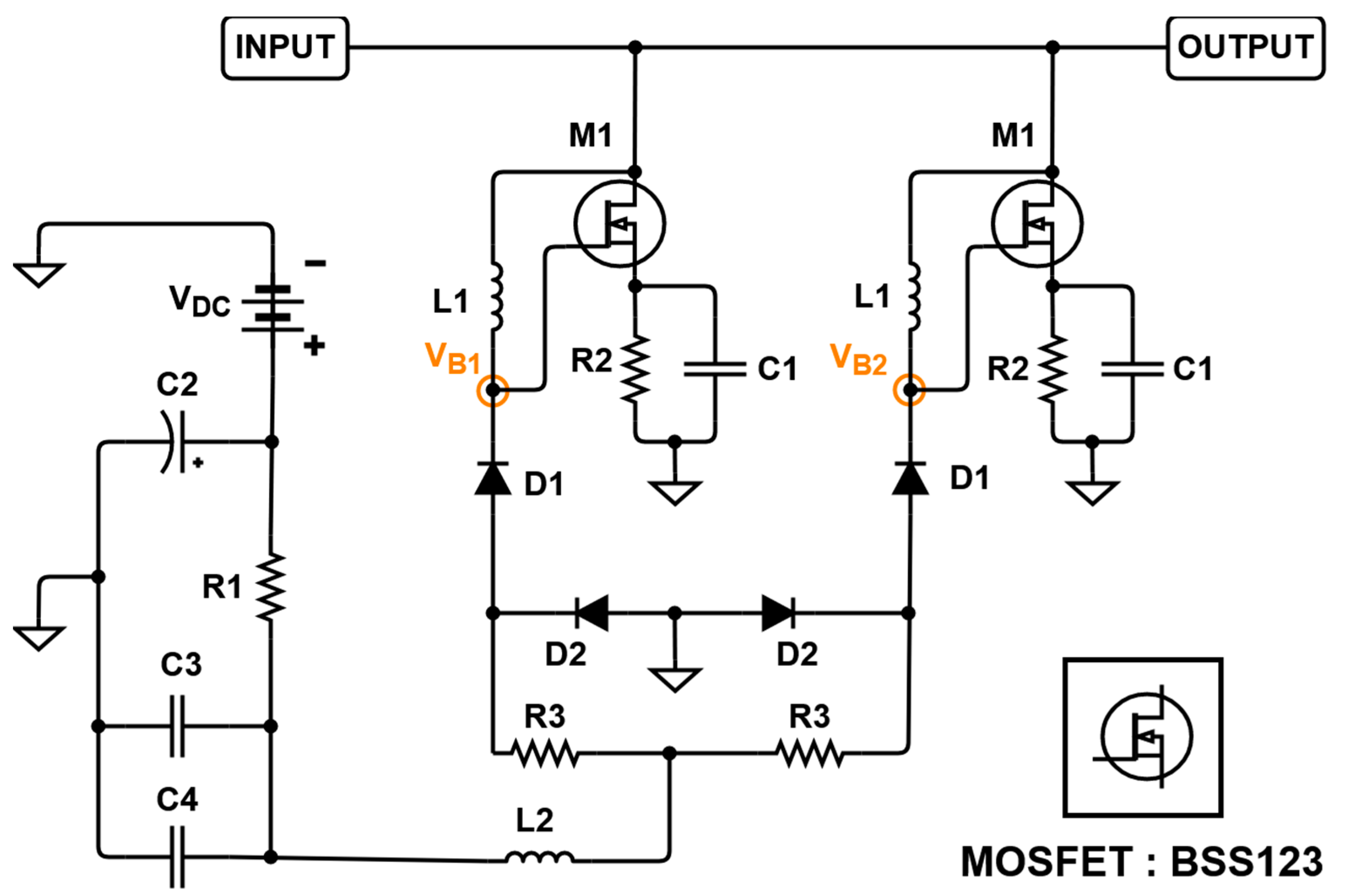
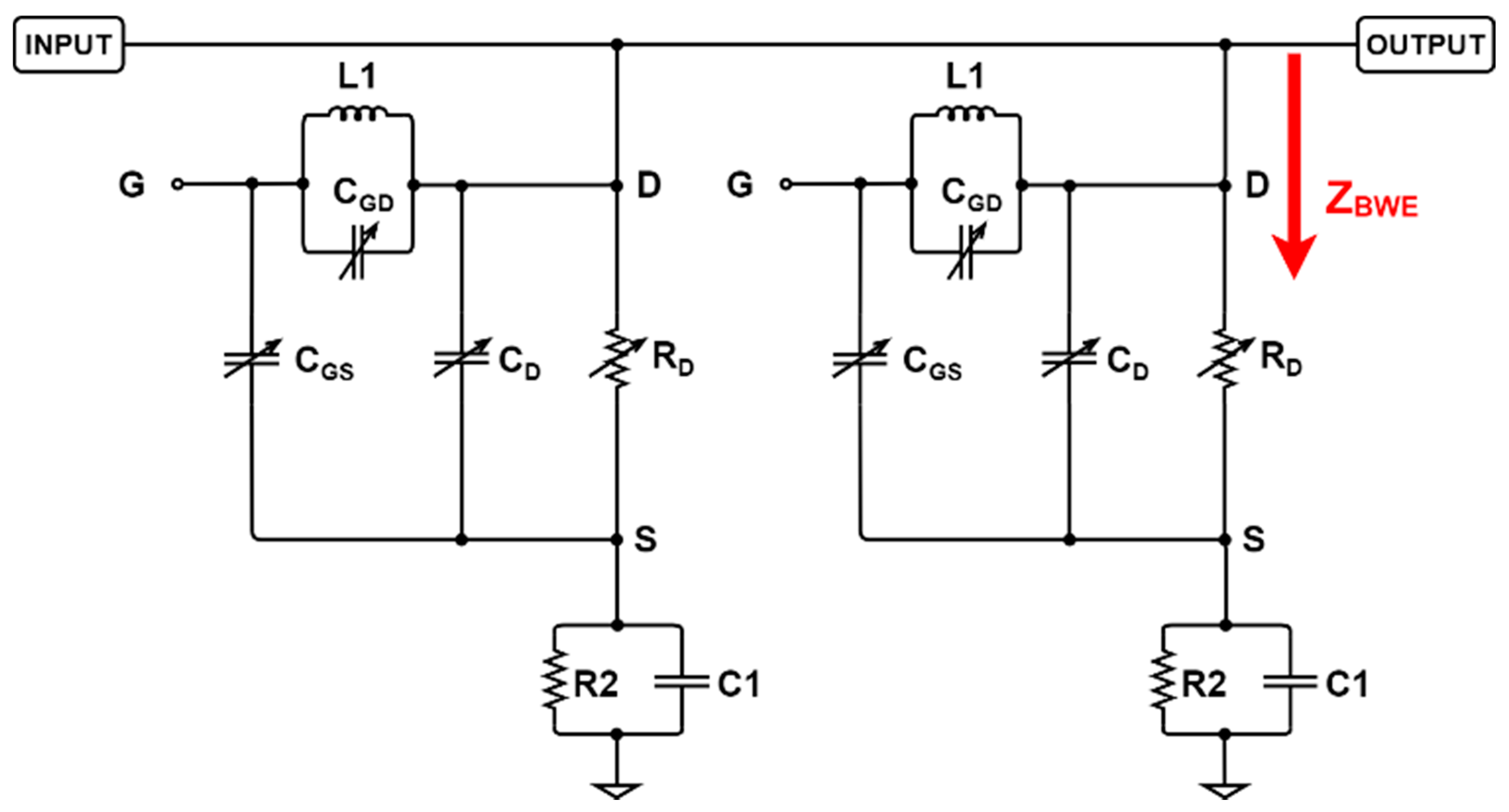
Figure 4 shows a schematic diagram of the designed BWE to show the circuit element values. Table 2 shows the numerical values of the resistors, capacitors, and inductor elements in Figure 4. R1 and R3 were used to be tuned to have proper voltage distribution and power consumption because M1 needs to be operated properly. The input signal was connected to the gate of M1 to form a feedback loop and can cause oscillation to be blocked through L1. However, the too high value of inductance may distort the input signal, so we properly selected the inductor value. R2 and C1 play a major role to lower the input impedance because the drain and source of M1 are shorted. If the impedance is too low, signal amplitude can be reduced. Thus, we properly selected those values for an input signal of 15 MHz. This circuit is added to the circuit, as shown in Figure 3, and thus the amplifier performance by applying different constant DC voltages is changed depending on the MOSFET (M1, BSS123) operation. When this circuit is assumed to be an ideal current source or ideal switch, the DC bias voltage VB1 in the BWE circuit operates the transistor, M1, as described below [36,37,38]:
where VD1(TH) and VSD are the threshold voltage and drain-source diode forward voltage, respectively. Above a certain voltage, VB1 shortens the drain and source of M1. As the drain and source voltages at M1 are short-circuited, C1, R2, and L1, and the capacitance and on-state resistance inside M1 are connected in parallel to the input impedance.
2.2. Predicting Performance Results
Changes in the performance of the amplifier only and the amplifier with BWE can be expected and compared based on pole calculations. Therefore, the equivalent circuit models of the LDMOSFET in the amplifier and the MOSFET in the BWE were simplified to calculate the poles. First, the input impedance (ZIN,basic) of the amplifier (Figure 5) was calculated as follows:
where XCG1 and XCG2 are the impedances of the capacitors, and XLG1 is the impedance of the inductor (see Figure 5). When the VDC is applied to M1, the VPP of the input signal is blocked at D1 because the DC level is increased by VB1, as shown in Figure 4. In addition, the gate of M1 is short-circuited due to the applied VDC. The on-state resistance RD and internal capacitances CGD, CGS, and CD exist. When M1 in the BWE circuit operates, it is expressed as an equivalent circuit for the AC analysis. Here, ZBWE indicates the impedance of the equivalent circuit when the circuit operates and is expressed as follows:
The input impedance in the BWE circuit was operated with parallel circuits, as shown in Figure 5.
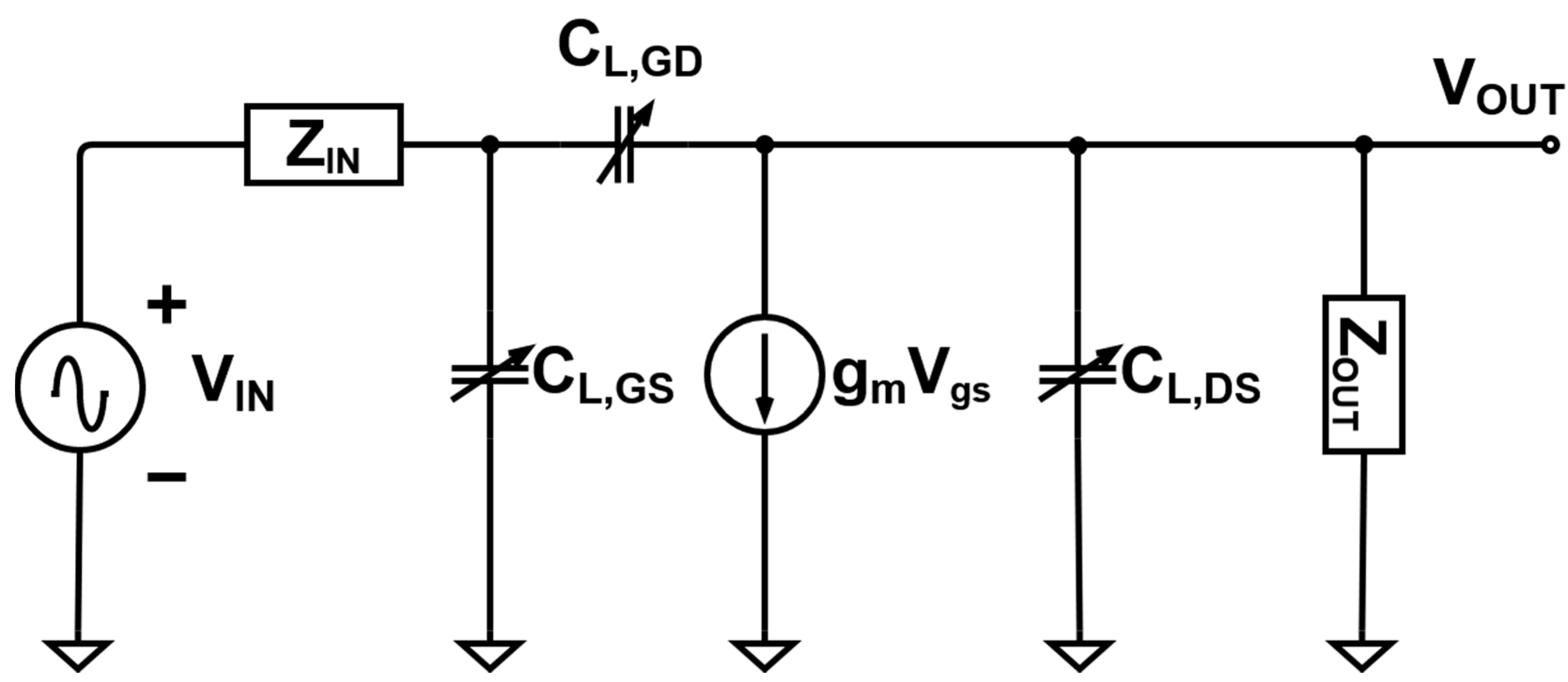
Figure 6 shows the equivalent circuit model of the amplifier [17]. Assuming that the bias voltage VB of the amplifier only, and the amplifier with BWE are assumed to be the same, the internal capacitances CL,GD, CL,GS, CL,DS, and gmVgs are the same.
As a result, the input and output poles and the transfer function can be predicted. The input pole of the amplifier only and the amplifier with the BWE circuit are given by Equation (6).
The output impedances of the amplifier only and the amplifier with the BWE circuit are assumed to be the same. The currents flowing from drain to source in the main transistor are the same if the same bias voltage is applied to both the amplifier and amplifier + BWE; the internal capacitance (Ciss, Coss, and Crss) is also the same. Thus, the internal capacitances (CL,GD, CL,GS, CL,DS, and gmVgs) are supposed to be the same. Therefore, the output impedances of the amplifier and amplifier + BWE are the same as ZOUT. Irrelevant to a transducer, the output signal does not change. Consequently, the output poles in the transfer functions of the amplifier only and the amplifier with the BWE circuit are expressed in Equations (8)–(10).
Equation (11) shows that ZIN,BWE has a relatively lower impedance than ZIN,basic because ZBWE is connected in parallel to ZIN,basic. Looking at Equations (6) and (7), the input pole has an inversely proportional relationship with the input impedance. Furthermore, from Equations (9) and (10), the transfer function has a proportional relationship with the input pole. As a result, the pole and transfer functions due to the different input impedances can be predicted as follows:
However, the predicted results should be operated in an ideal environment. The actual results are extremely different from the predicted results because the high-voltage amplifier operations are not accurately predictable due to several high-voltage environment variables such as parasitic impedances, high-voltage valuable variances, and unpredictable equivalent inductance models [39,40].
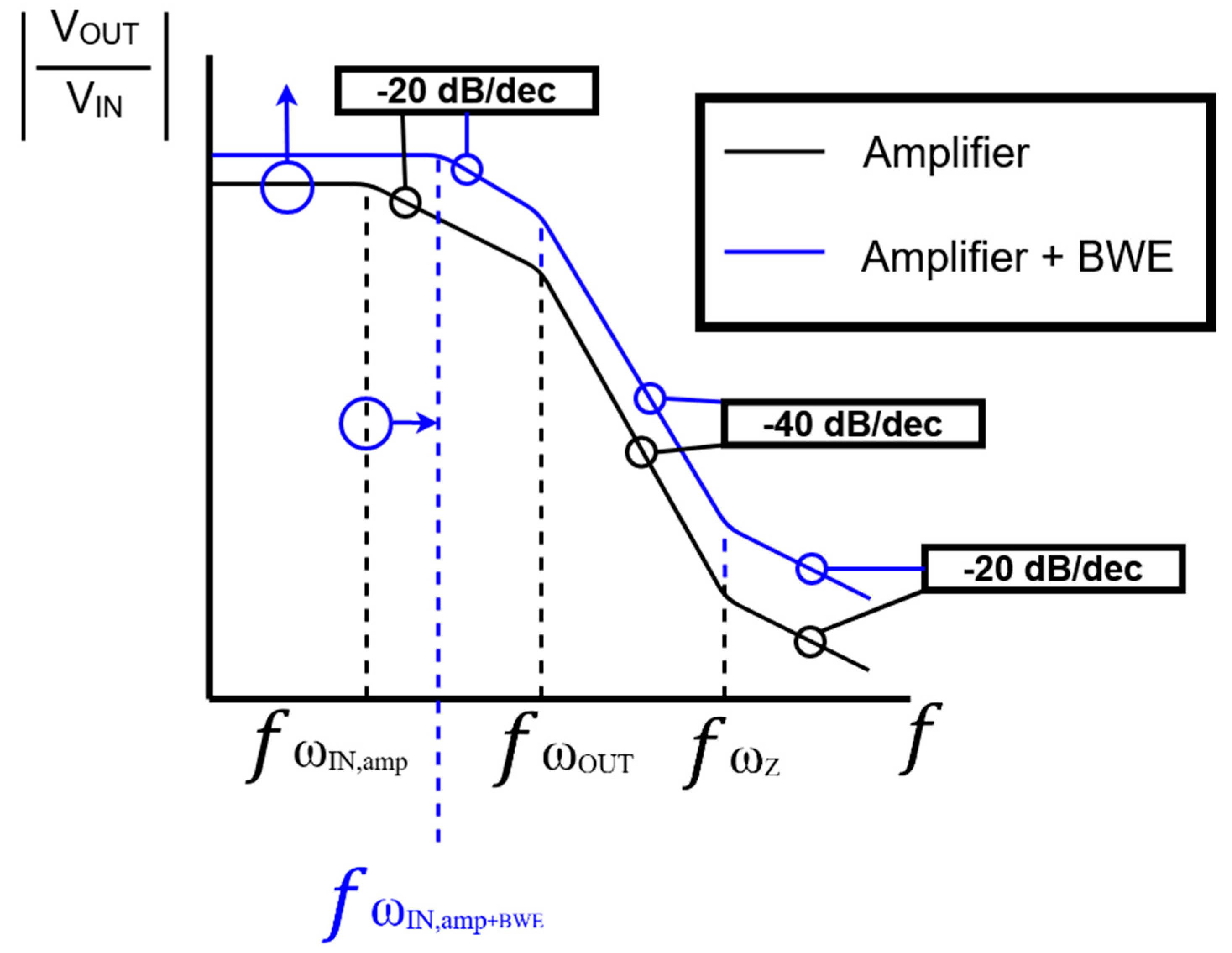
Figure 7 shows the predicted graph based on Equations (11)–(13). By adding a BWE circuit to the existing amplifier, the magnitude and input pole in the transfer function increase. In Figure 7, the entire line goes up, and the input pole moves to the right. As a result, we assume that the line decreases by 20, 40, and 20 dB/dec, respectively, in the interval between the input pole, the output pole, and the zero point. Comparing the two cases, the transfer function is expected to increase. As the pole location shifts, we can expect to achieve a wider bandwidth.
2.3. Experimental Measurement Process
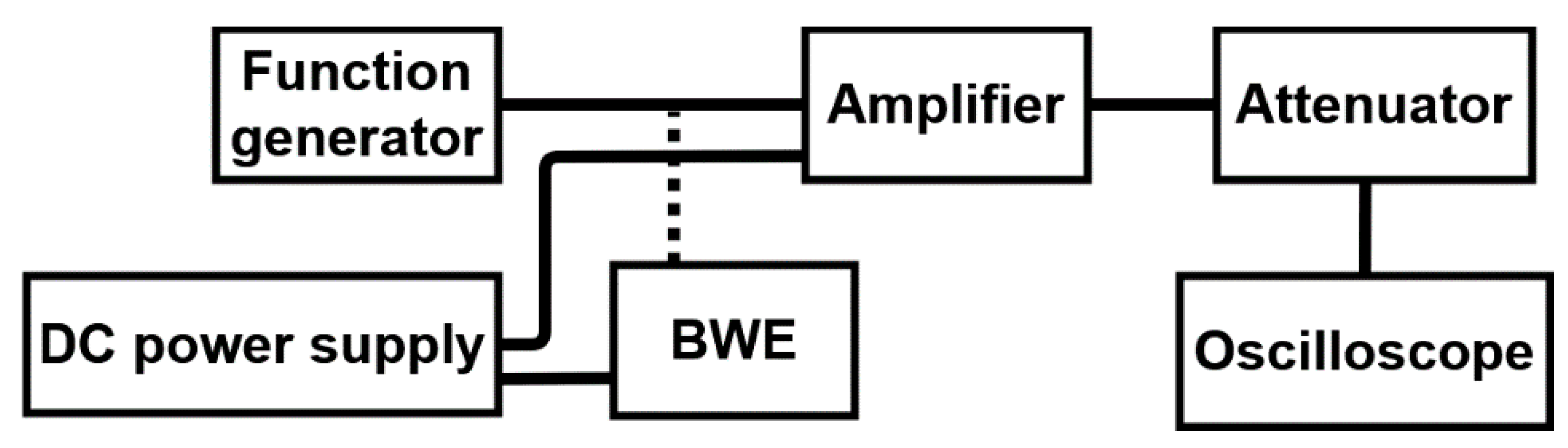
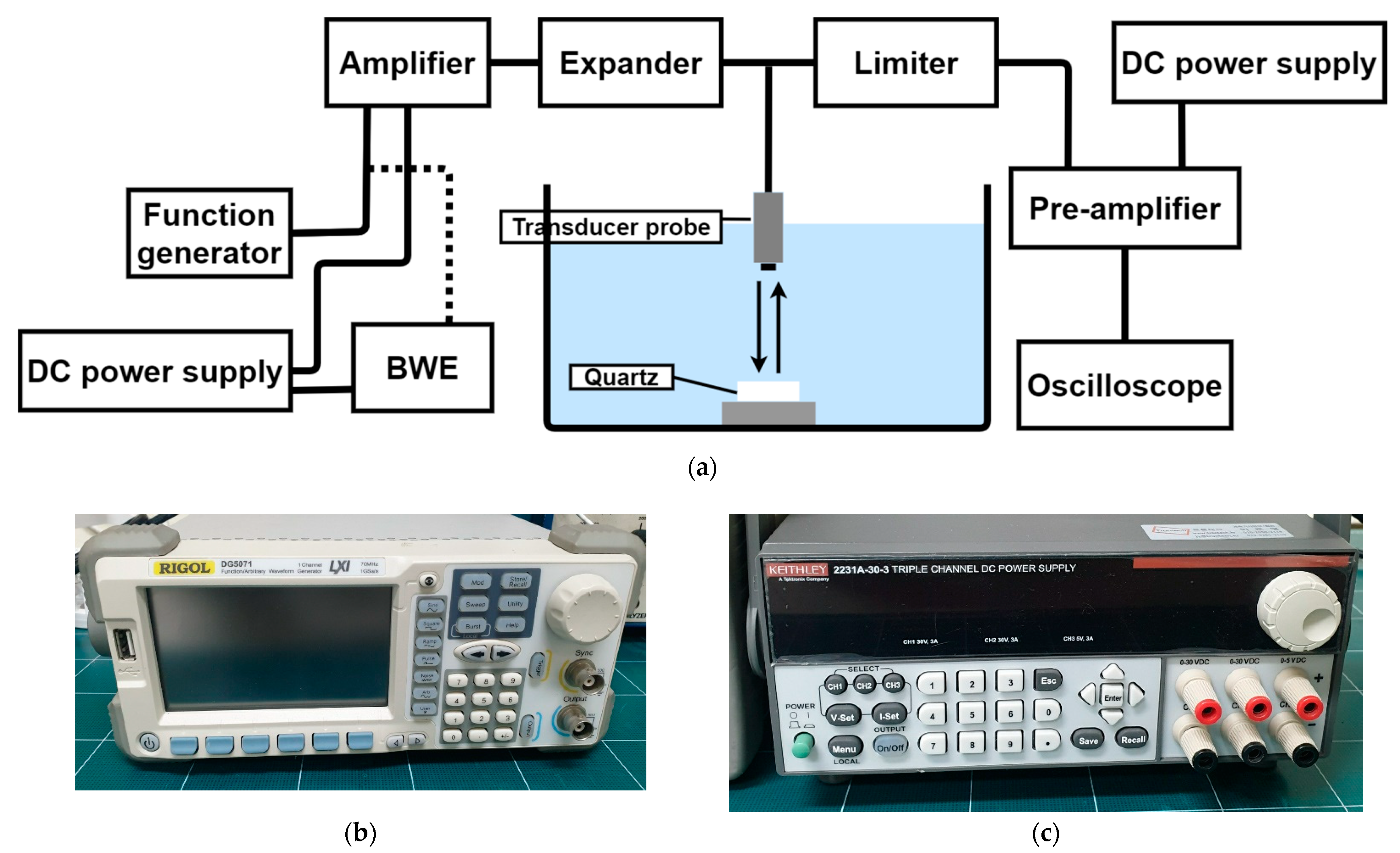
Figure 8 shows a block diagram showing the performance measurement of the amplifier only and the amplifier with BWE circuits. A function generator, DC power supply, attenuator, and oscilloscope were used to measure the performance of the designed circuits. A BWE circuit was installed between the function generator and amplifier. The BWE circuit operates when DC power is supplied by the power supply. The amplified signal can cause damage to the oscilloscope from a high voltage of 5 VP-P or greater. Therefore, the output signals were attenuated by a 40 dB attenuator, and the performances were measured using an oscilloscope [41,42,43]. To measure the performance of the amplifiers, the frequency and input signal amplitudes were adjusted using a function generator. In addition, the voltage gain was obtained from the measured output signals. As a result, the outputs of the amplifier and BWE circuit-equipped amplifier were measured and compared. The voltage gain is a performance indicator for measuring the performance of an amplifier, and its high output helps to provide a clear ultrasound image [44,45,46]. In addition, the bandwidth of the gain over frequency of the amplifier only and the amplifier equipped with the BWE circuit can be compared. The output signal is an important performance indicator of an ultrasonic transmitter because it shows the sensitivity of the system.
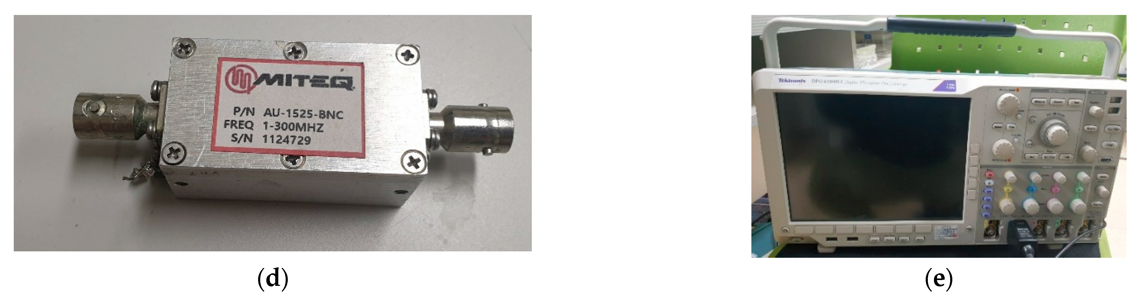
Figure 9a shows the measurement procedures used to obtain the echo signal of the transducer with the designed amplifier with and without a BWE circuit. Various instruments have been used to measure the echo signal to determine its compatibility with ultrasonic transducer probes [47]. The amplified signal was passed through the expander [48,49]. The signal was transmitted through the transducer probe and reflected by the quartz to be received [50,51,52]. The expander was used to remove the noise and reduce the ringdown signal from amplified signals [53,54,55]. Since the received signal has an extremely low amplitude, it is amplified by an approximately 32 dB gain pre-amplifier and then displayed on the oscilloscope. During this process, because quartz reflects more than 99% of the signal, the data of the echo signal can be measured to estimate the amplifier performance [56,57]. The amplified signal, called a discharged signal, is required to vibrate the piezoelectric element of the transducer probe; however, it is not necessary to measure the echo signal, and the oscilloscope can be damaged with a voltage of higher than 5 VP-P, and thus, it is minimized using a limiter [58,59,60]. Figure 9a,b shows the tested equipment components used in Figure 9a.
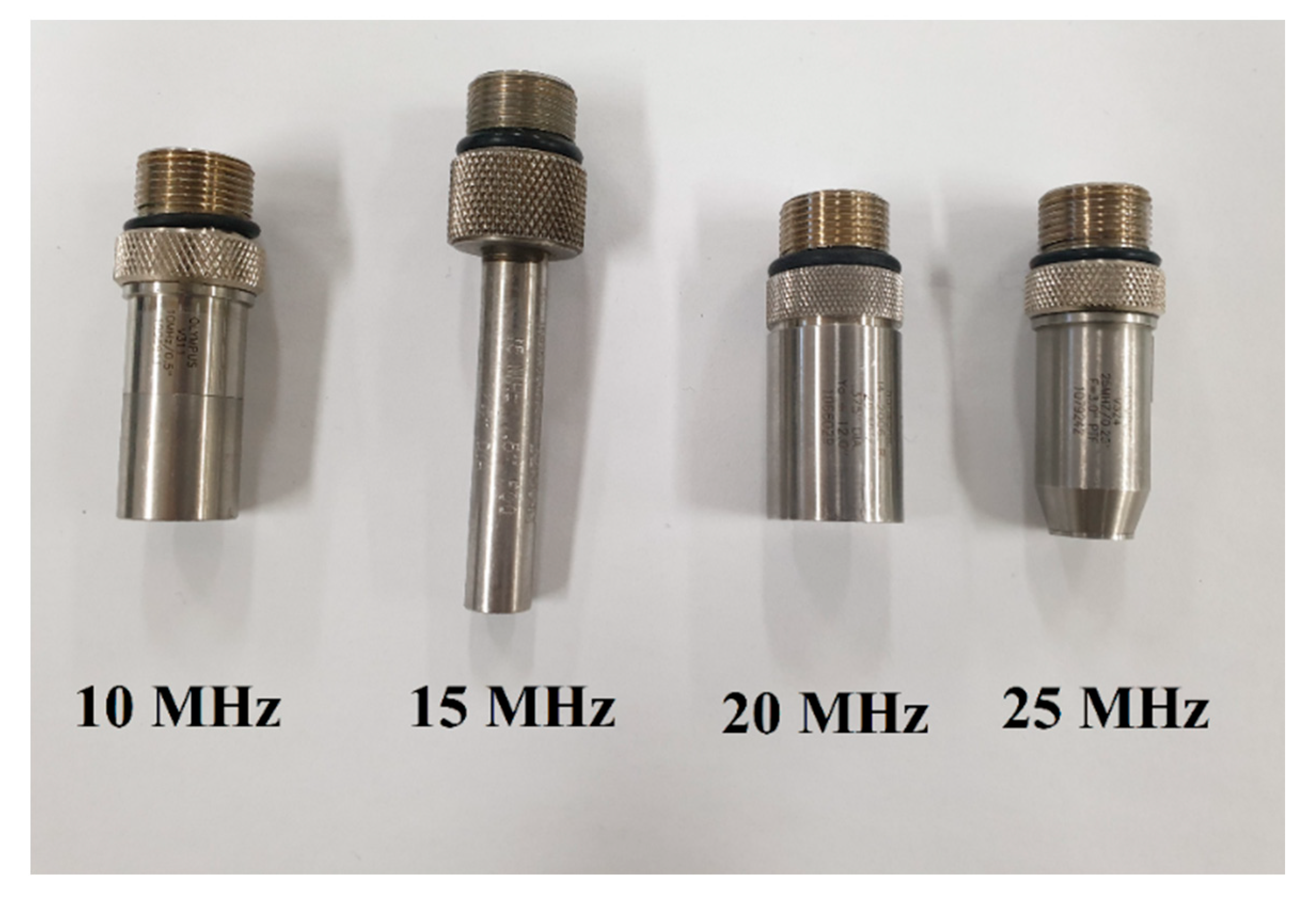
In Figure 10, the transducer probe was used to measure the echo signal to estimate the amplifier equipped with and without the BWE circuit. The amplifier performance was measured by adjusting the input signal frequency according to the resonance frequency of each transducer [61,62,63]. All input parameters are the same when the amplifier is equipped with and without the BWE circuit. The measured performances are the amplitudes and pulse widths of the echo signals, −6 dB bandwidths, and harmonic components using a fast Fourier transform (FFT). The harmonic distortion characteristics were estimated using the total harmonic distortion (THD) equation [64,65,66]:
where the second and third harmonics are the amplitudes of the second and third harmonic distortion components, and the fundamental signal is the amplitude of the fundamental signal at the desired operating frequency.
The higher the amplitude of the echo signal is, the higher the sensitivity of the transducer probe [47,67]. The narrower pulse width of the echo signal can result in a higher axial resolution of the transducer probe. The lateral resolution is related to the bandwidth [68]. The wider the bandwidth at the −6 dB point, the lower the Q factor, and thus, more image data can be realized [69]. However, the harmonic component generated unwanted image data [70,71]. Thus, these data need to be minimized. In this study, the measured performance factors were compared according to each transducer at different frequencies, as shown below. Therefore, the amplitudes, pulse widths, bandwidths, and THD were measured and compared by applying different transducer probes according to the frequency of each input signal with an amplifier equipped with and without the BWE circuit.
3. Results
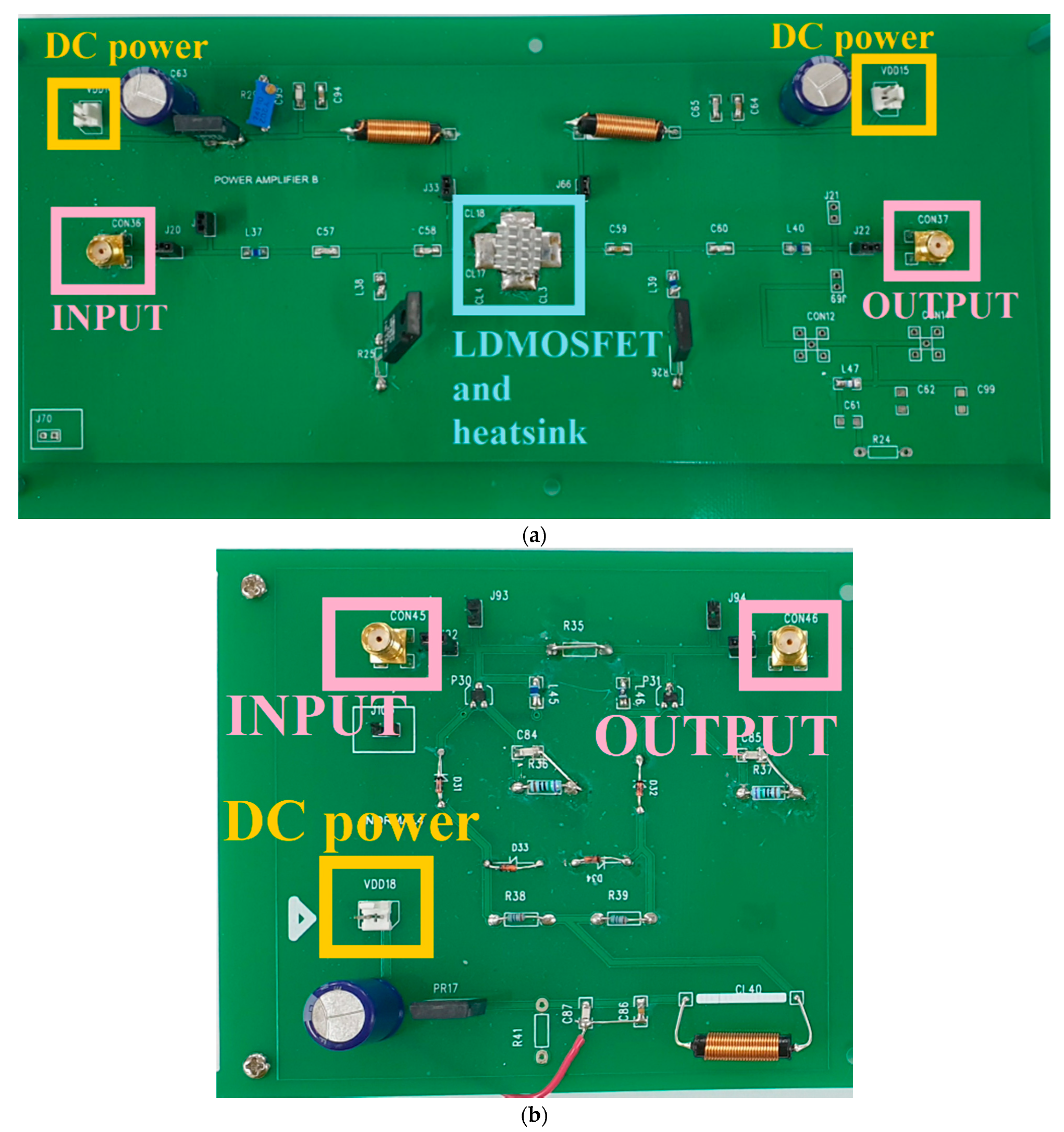
Figure 11a,b shows the manufactured single-ended power amplifier and BWE circuits, respectively. The main transistor (LDMOSFET) with a heatsink was used to release heat more effectively [72,73,74]. The output port in Figure 11b is connected to the input port, as shown in Figure 11a.
3.1. Performance Comparison and Analysis of the Amplifier Only and Amplifier + BWE Circuit
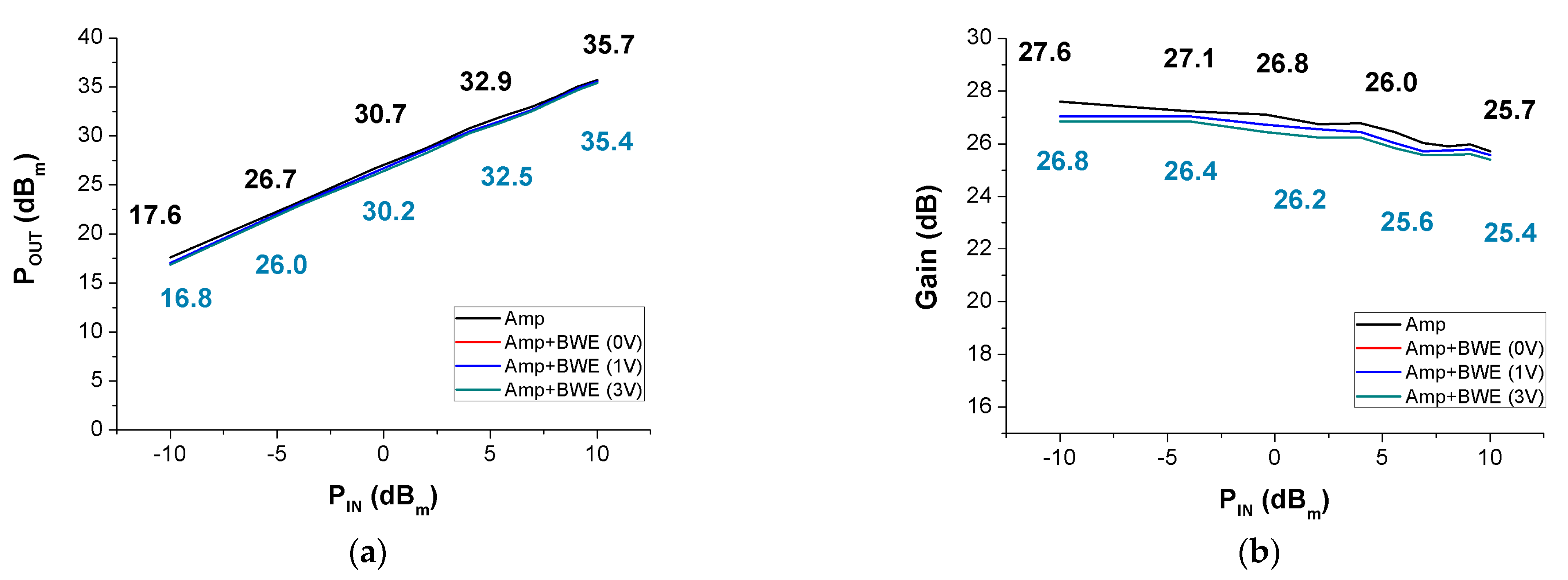
Figure 12a,b shows the POUT and gain variances as the input signal increases. The black line shows the performance of the power amplifier. The red, blue, and khaki lines show the performance of the amplifier with the BWE circuit using 0V, 1V, and 3V DC, respectively. In the case of amp + BWE (0 V) and amp + BWE (1 V), the active device of the BWE (see M1 in Figure 4) is not in operation, and thus, they have almost the same performance. Therefore, the red line is almost identical to the blue line. In Figure 12a,b, the performance of the power amplifier has a higher POUT and gain than the amplifier with a BWE (3 V) of between −10 dBm and 10 dBm.
Figure 12c,d shows the POUT and gain according to frequency variations at an input power of −6.5. In Figure 12c,d, the performances of the amplifier at 5–16 MHz have a higher POUT and gain than the power amplifier with BWE (3 V). The performance of the power amplifier with a BWE (3 V) has a higher POUT and gain of 17–35 MHz, compared to the power amplifier only. The POUT of the power amplifier with BWE (3V) outperformed that of the power amplifier after 16.132 MHz. In addition, the −3 dB POUT bandwidth of the power amplifier only and the power amplifier with BWE (3 V) were 51.5% and 81.5%, respectively. The −3 dB gain bandwidth of the power amplifier only and the power amplifier with BWE (3 V) are 84.1% and 141%, respectively. By incorporating the BWE circuit into the power amplifier, the POUT decreases to 0.8 dBm, and the gain decreases by 0.8 dB when the PIN is −10 dBm. Theoretically, the magnitude of the transfer function increases with the addition of the BWE circuit to the power amplifier. Although the POUT and gain should be increased together, in practice, the final output signal can be slightly reduced because of the power loss of the passive components in the BWE circuit. However, in the graphs of the POUT and gain versus frequency, the POUT bandwidth increases by approximately 30%, and the gain bandwidth increases by approximately 56.9%. In this paper, the BWE circuit is used to widen the bandwidth by lowering the input impedance of the power amplifier. However, it does not decrease input impedance linearly at all frequencies. As shown in the experimental results, the bandwidth at the high-frequency range is wider than that of the low-frequency range because the BWE circuit has more impedance reduction at high frequency (See Figure 12c,d)
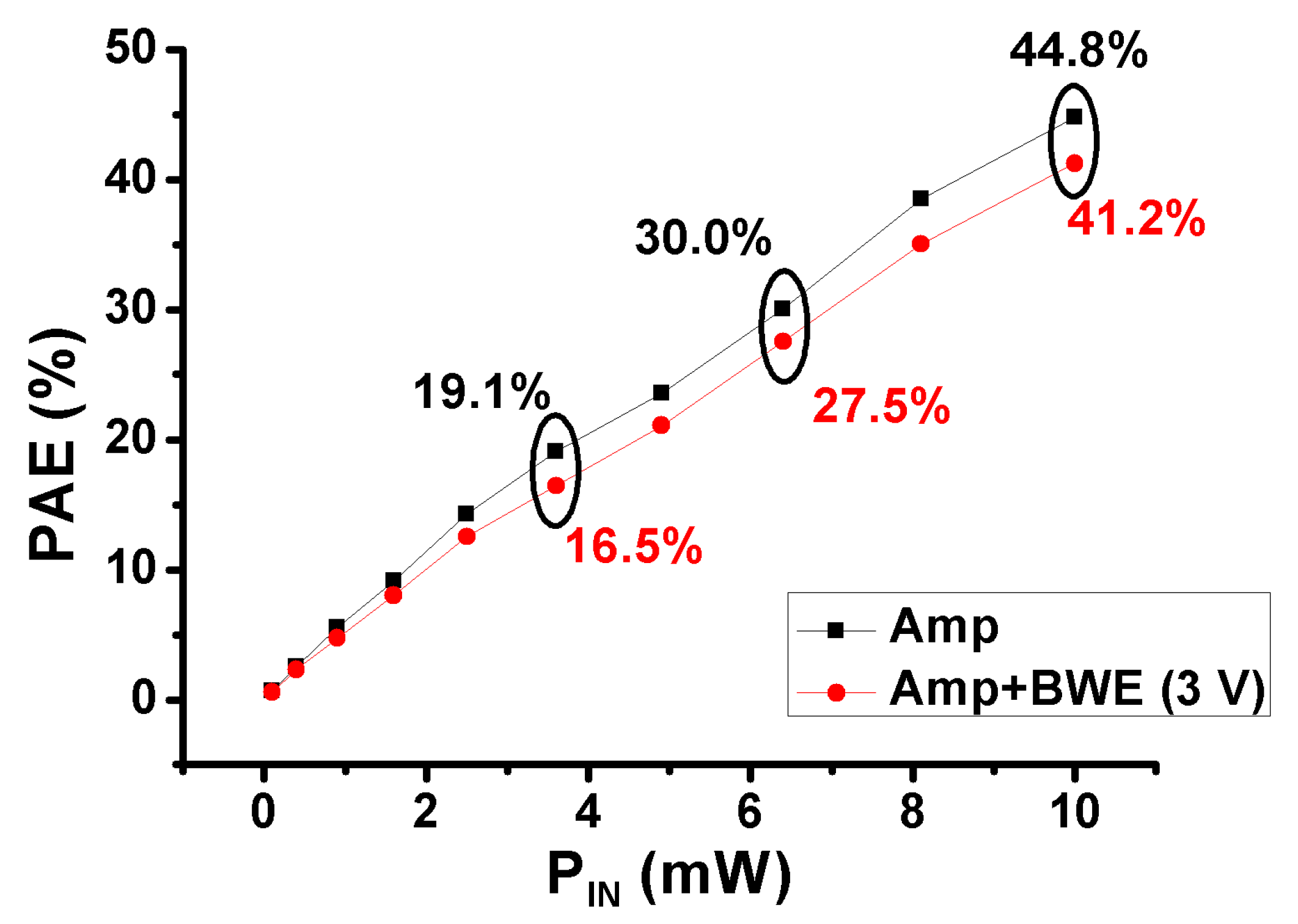
Figure 13 is the graph of the power added efficiency (PAE) of the amp and the amp + BWE (3 V) at 15 MHz. The PAE indicates how much DC power was used to amplify the input signal [15,75]. In Figure 13, the PAE versus PIN of the amp (44.8%) is higher than the amp + BWE (3 V) (41.2%) when 10 dBm input power is applied. This is because the additional DC power is used for the designed BWE, and the amp has a higher POUT versus the PIN than the amp + BWE (3 V). As a result, the PAEs of the amp and the amp + BWE (3V) do not show a big difference between them.
3.2. Echo Signal Performance Comparison and Analysis
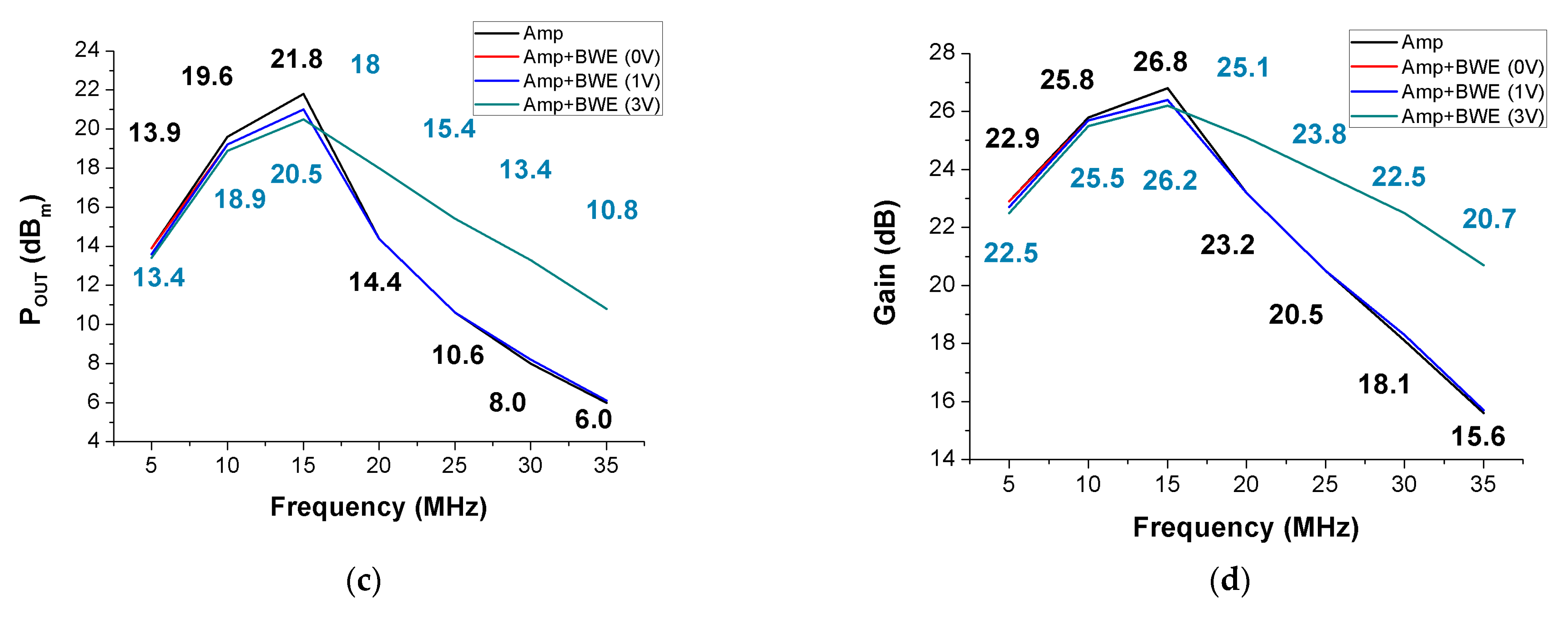
Figure 14 shows measured echo signal performances when using 10, 15, 20, and 25 MHz ultrasound transducers. When the ultrasound transducers with the same frequency were used, the distance to the target was exactly the same. The input signal was measured using a four-cycle burst wave with a suitable resonant frequency for the transducer probes. The measurement environment of each frequency is the same except for the presence of BWE with different DC voltages. As shown in Figure 14, the red, blue, and khaki lines show the performance of the power amplifier only and the power amplifier with BWE circuit using 0 V, 1 V, and 3V DC, respectively. In the case of the amplifier + BWE (0 V) and amplifier + BWE (1 V), the MOSFET (referring to M1 in Figure 4), which is the active device of the BWE circuit, is not operated and thus shows almost the same performances.
Figure 14a,b shows the measured results of the pulse widths and amplitudes over the time scale. Figure 14a shows the pulse width according to the frequency. The experimental results showed no significant difference in any of the measured frequency bands. Experimentally, the BWE circuit does not have a significant influence on the pulse width of the echo signals. Figure 14b shows the measured echo amplitudes of the peak-to-peak voltage according to the frequency using a 32 dB preamplifier. As shown in the graph, the amplitude of amp + BWE (3 V) was higher than that of the amp after 15 MHz. At 25 MHz, there is a difference of approximately 2.4 dBm. Since the echo signal has an extremely low amplitude, a 2.4 dBm increment in the amplitude is an attractive result.
Figure 14c,d shows the calculated FFT data used to measure the harmonics and −6 dB bandwidths of the measured echo signals. Figure 14c shows the THD (%) according to the frequency. At 20 MHz, the THD of the amp was calculated as 7.15%, which is less than that of the amp + BWE (3 V). However, at 25 MHz, the THD of the amp was calculated as 15.63%, and that of the amp + BWE (3 V) was calculated as 5.74%. Figure 14d shows the echo bandwidth according to the frequency. By adding a BWE (3 V) circuit to the power amplifier, the −6 dB bandwidth of the echo signal was increased by 0.7%, 8.1%, 6.0%, and 9.8% at 10, 15, 20, and 25 MHz, respectively. The bandwidth of the echo signal is actually related to the axial resolution of the ultrasound image, and thus, a wider bandwidth can possibly improve the axial resolution [11]. By adding a BWE circuit to the power amplifier, the bandwidth of the echo signal is increased, which can help improve the quality of the echo signals.
Both low and high-frequency transducers can be utilized by using the proposed BWE circuit with the amplifier. There are some ultrasound applications that utilize dual-band transducer applications [76]. For these applications, the signals of low- and high-frequency ranges from dual-band therapeutic/imaging transducer applications need to be obtained. From the paper, the ultrasound transducers enable therapeutic and imaging modes if needed. A treatment application requires to use many cycle sinusoidal waveforms [77]. The harmonic components generated when amplifying the input signal can affect the signal quality of the echo signals [78]. For low-frequency therapeutic applications, the harmonic components can distort the signal and attenuate the depth of penetration [79]. Therefore, the amplifiers used for therapeutic applications are preferred to have a narrow bandwidth in order to minimize harmonic components. For high-frequency imaging applications, the wider bandwidth, the higher axial resolution can be achieved [80]. Therefore, an amplifier with wide bandwidth is preferred. Hence, our proposed scheme could be useful for such dual-band transducer applications.
4. Conclusions
The transducers used in ultrasound systems have their own different frequency bands, depending on the particular purpose and testing area. Therefore, it is necessary to use an electrical circuit with a wide bandwidth such that the output signal of the transmitter can cover various ultrasound transducers. One way of expanding the bandwidth is impedance matching. Impedance matching is required to maximize the amplitudes or bandwidths of the output signals to the transducer. However, an impedance-matching job that can cover such wide transducers is extremely difficult because the impedance is different for each transducer. Although impedance matching is not taken into account in this document, it is clear that impedance matching can be used if we know the impedance values of the predetermined transducer. However, this method used to increase the bandwidth could possibly lower the output amplitude at the center frequency. In addition, the feedback loop circuit methodology can increase the bandwidth by reducing the output amplitude of the power amplifier. Therefore, we propose a switching mode transmit circuit that can widen the bandwidth and minimize the output amplitude as needed. The designed BWE circuit changes the performance of the power amplifier because the bandwidth in the transfer function is widened by moving the input pole of the power amplifier.
To verify our proposed concept and verify the performance results, we tested a power amplifier equipped with a BWE circuit under the same conditions. Comparing the performances of the manufactured amplifier only and the amplifier with the BWE circuit, the POUT and gain values of the amplifier with the BWE circuit were decreased slightly to 0.8 dBm and 0.8 dB; however, the POUT bandwidth increased by approximately 30%, and the gain bandwidth increased by approximately 56.9% at −6.5 dBm of input power. In addition, the echo bandwidths were expanded by 0.7%, 8.1%, 6.0%, and 9.8% at frequencies of 10, 15, 20, and 25 MHz, respectively.
In practice, the measured experimental data may be different from the theoretical data because there are various side effects caused by signal distortions of different frequency characteristics and parasitic components of the elements. From the experimental results, none of the measured performances were enhanced when adding a functional BWE circuit. Although the bandwidth is wider, there is a slight compromise, such as a decline in output power or an increase in THD (%). However, the manufactured BWE circuit improves the bandwidth and minimizes the amplitude of the power amplifier to support higher operating transducer probes, thus possibly helping improve the ultrasound system resolution.
Author Contributions
Conceptualization, K.K. and H.C.; methodology, K.K. and H.C.; formal analysis, K.K.; writing—original draft preparation, K.K. and H.C. All authors have read and agreed to the published version of the manuscript.
Funding
This work was supported by a National Research Foundation of Korea grant funded by the government (MSIT) (No. 2020R1A2C4001606). This work was supported by project for Industry-Academic Cooperation Based Platform R&D funded Korea Ministry of SMEs and Startups in 2020 (Project No. S3010583).
Institutional Review Board Statement
Not applicable.
Informed Consent Statement
Not applicable.
Data Availability Statement
The data presented in this study are available on request from the corresponding author.
Conflicts of Interest
The authors declare no conflict of interest.
References
- Shung, K.K. Diagnostic Ultrasound: Imaging and Blood Flow Measurements; Taylor & Francis: Boca Raton, FL, USA, 2015. [Google Scholar]
- Szabo, T.L. Diagnostic Ultrasound Imaging: Inside Out; Elsevier Academic Press: London, UK, 2013. [Google Scholar]
- Zhou, Q.; Lau, S.; Wu, D.; Shung, K.K. Piezoelectric films for high frequency ultrasonic transducers in biomedical applications. Prog. Mater. Sci. 2011, 56, 139–174. [Google Scholar] [CrossRef] [PubMed] [Green Version]
- Zhu, B.; Fei, C.; Wang, C.; Zhu, Y.; Yang, X.; Zheng, H.; Zhou, Q.; Shung, K.K. Self-focused AlScN film ultrasound transducer for individual cell manipulation. ACS Sens. 2017, 2, 172–177. [Google Scholar] [CrossRef] [PubMed]
- Hoskins, P.R.; Martin, K.; Thrush, A. Diagnostic Ultrasound: Physics and Equipment; Cambridge University Press: Cambridge, UK, 2019. [Google Scholar]
- Postema, M. Fundamentals of Medical Ultrasound; Taylor and Francis: New York, NY, USA, 2011. [Google Scholar]
- Kremkau, F.W.; Forsberg, F. Sonography Principles and Instruments; Elsevier Health Sciences: Amsterdam, The Netherlands, 2015. [Google Scholar]
- Li, X.; Wei, W.; Zhou, Q.; Shung, K.K.; Chen, Z. Intravascular photoacoustic imaging at 35 and 80 MHz. J. Biomed. Opt. 2012, 17, 106005. [Google Scholar] [CrossRef] [Green Version]
- Ritter, T.A.; Shrout, T.R.; Tutwiler, R.; Shung, K.K. A 30-MHz piezo-composite ultrasound array for medical imaging applications. IEEE Trans. Ultrason. Ferroelectr. Freq. Control. 2002, 49, 217–230. [Google Scholar] [CrossRef]
- Kim, J.; You, K.; Choi, H. Post-Voltage-Boost Circuit-Supported Single-Ended Class-B Amplifier for Piezoelectric Transducer Applications. Sensors 2020, 20, 5412. [Google Scholar] [CrossRef] [PubMed]
- Bushberg, J.T.; Boone, J.M. The Essential Physics of Medical Imaging; Lippincott Williams & Wilkins: Philadelphia, PA, USA, 2011. [Google Scholar]
- Zagzebski, J.A. Essentials of Ultrasound Physics; Mosby: Maryland Heights, MO, USA, 1996. [Google Scholar]
- Lee, T.H. The Design of CMOS Radio-Frequency Integrated Circuits; Cambridge University Press: Cambridge, UK, 2006. [Google Scholar]
- Razavi, B. Design of Analog CMOS Integrated Circuits; McGraw-Hill Science: New York, NY, USA, 2016. [Google Scholar]
- Razavi, B. RF Microelectronics; Prentice Hall: Upper Saddel River, NJ, USA, 2011. [Google Scholar]
- Albulet, M. RF Power Amplifiers; SciTech Publishing: London, UK, 2001. [Google Scholar]
- Grebennikov, A. RF and Microwave Power Amplifier Design; McGraw-Hill: New York, NY, USA, 2005. [Google Scholar]
- Katz, A. Linearization: Reducing distortion in power amplifiers. IEEE Microw. Mag. 2001, 2, 37–49. [Google Scholar] [CrossRef]
- Cripps, S.C. RF Power Amplifiers for Wireless Communications; Artech House: Norwood, MA, USA, 2006. [Google Scholar]
- Reynaert, P.; Steyaert, M. RF Power Amplifiers for Mobile Communications; Springer Science & Business Media: Berlin, Germany, 2006. [Google Scholar]
- Park, J.; Hu, C.; Li, X.; Zhou, Q.; Shung, K.K. Wideband linear power amplifier for high-frequency ultrasonic coded excitation imaging. IEEE Trans. Ultrason. Ferroelectr. Freq. Control. 2012, 59, 825–832. [Google Scholar] [CrossRef]
- Gao, Z.; Gui, P.; Jordanger, R. An integrated high-voltage low-distortion current-feedback linear power amplifier for ultrasound transmitters using digital predistortion and dynamic current biasing techniques. IEEE Trans. Circuits Syst. II Express Briefs 2014, 61, 373–377. [Google Scholar] [CrossRef]
- Choi, H. Development of a Class-C Power Amplifier with Diode Expander Architecture for Point-of-Care Ultrasound Systems. Micromachines 2019, 10, 697. [Google Scholar] [CrossRef] [Green Version]
- Agbossou, K.; Dion, J.-L.; Carignan, S.; Abdelkrim, M.; Cheriti, A. Class D Amplifier for a Power Piezoelectric Load. IEEE Trans. Ultrason. Ferroelectr. Freq. Control. 2000, 47, 1036–1041. [Google Scholar] [CrossRef]
- Yuan, T.; Dong, X.; Shekhani, H.; Li, C.; Maida, Y.; Tou, T.; Uchino, K. Driving an inductive piezoelectric transducer with class E inverter. Sens. Actuators A 2017, 261, 219–227. [Google Scholar] [CrossRef]
- Moon, J.-Y.; Lee, J.; Chang, J.H. Electrical impedance matching networks based on filter structures for high frequency ultrasound transducers. Sens. Actuators A 2016, 251, 225–233. [Google Scholar] [CrossRef]
- Huang, H.; Paramo, D. Broadband electrical impedance matching for piezoelectric ultrasound transducers. IEEE Trans. Ultrason. Ferroelectr. Freq. Control. 2011, 58, 2699–2707. [Google Scholar] [CrossRef] [PubMed]
- Zhou, Q.; Lam, K.H.; Zheng, H.; Qiu, W.; Shung, K.K. Piezoelectric single crystal ultrasonic transducers for biomedical applications. Prog. Mater. Sci. 2014, 66, 87–111. [Google Scholar] [CrossRef] [PubMed] [Green Version]
- Vuolevi, J.; Rahkonen, T. Distortion in RF Power Amplifiers; Artech house: London, UK, 2003. [Google Scholar]
- Chang, K. Microwave Solid-State Circuits and Applications; Wiley: New York, NY, USA, 1994. [Google Scholar]
- Kazimierczuk, M.K. RF Power Amplifier; John Wiley & Sons: Hoboken, NJ, USA, 2014. [Google Scholar]
- Malik, N.R. Electronic Circuits: Analysis, Simulation, and Design; Prentice Hall: Englewood Cliffs, NJ, USA, 1995. [Google Scholar]
- Self, D. Audio Power Amplifier Design; Focal Press: Waltham, MA, 2013. [Google Scholar]
- Larson, L.E. RF and Microwave Circuit Design for Wireless Communications; Artech House: Norwood, MA, USA, 1996. [Google Scholar]
- Choe, S.-W.; Choi, H. Suppression Technique of HeLa Cell Proliferation Using Ultrasonic Power Amplifiers Integrated with a Series-Diode Linearizer. Sensors 2018, 18, 4248. [Google Scholar] [CrossRef] [Green Version]
- You, K.; Choi, H. Wide Bandwidth Class-S Power Amplifiers for Ultrasonic Devices. Sensors 2020, 20, 290. [Google Scholar] [CrossRef] [PubMed] [Green Version]
- Davidse, J. Analog Electronic Circuit Design; Prentice Hall: Upper Saddle River, NJ, USA, 1991. [Google Scholar]
- Ullah, M.N.; Park, Y.; Kim, G.B.; Kim, C.; Park, C.; Choi, H.; Yeom, J.-Y. Simultaneous Acquisition of Ultrasound and Gamma Signals with a Single-Channel Readout. Sensors 2021, 21, 1048. [Google Scholar] [CrossRef]
- Zhang, X.; Larson, L.E.; Asbeck, P. Design of Linear RF Outphasing Power Amplifiers; Artech House: Norwood, MA, USA, 2003. [Google Scholar]
- Cripps, S.C. Advanced Techniques in RF Power Amplifier Design; Artech House: Norwood, MA, USA, 2002. [Google Scholar]
- Kim, J.; You, K.; Choe, S.-H.; Choi, H. Wireless Ultrasound Surgical System with Enhanced Power and Amplitude Performances. Sensors 2020, 20, 4165. [Google Scholar] [CrossRef] [PubMed]
- Zawawi, R.B.A.; Abbasi, W.H.; Kim, S.-H.; Choi, H.; Kim, J. Wide-Supply-Voltage-Range CMOS Bandgap Reference for In Vivo Wireless Power Telemetry. Energies 2020, 13, 2986. [Google Scholar] [CrossRef]
- Chang-Hong, H.; Snook, K.A.; Poi-Jie, C.; Shung, K.K. High-frequency ultrasound annular array imaging. Part II: Digital beamformer design and imaging. IEEE Trans. Ultrason. Ferroelectr. Freq. Control. 2006, 53, 309–316. [Google Scholar] [CrossRef]
- Kim, J.; Kim, K.; Choe, S.-H.; Choi, H. Development of an Accurate Resonant Frequency Controlled Wire Ultrasound Surgical Instrument. Sensors 2020, 20, 3059. [Google Scholar] [CrossRef]
- You, K.; Kim, S.-H.; Choi, H. A Class-J Power Amplifier Implementation for Ultrasound Device Applications. Sensors 2020, 20, 2273. [Google Scholar] [CrossRef]
- Li, G.; Qiu, W.; Zhang, Z.; Jiang, Q.; Su, M.; Cai, R.; Li, Y.; Cai, F.; Deng, Z.; Xu, D. Noninvasive Ultrasonic Neuromodulation in Freely Moving Mice. IEEE Trans. Biomed. Eng. 2018, 66, 217–224. [Google Scholar] [CrossRef] [PubMed]
- Zhang, T.; Ou-Yang, J.; Yang, X.; Wei, W.; Zhu, B. High Performance KNN-Based Single Crystal Thick Film for Ultrasound Application. Electron. Mater. Lett. 2019, 15, 1–6. [Google Scholar] [CrossRef]
- Choi, H.; Choe, S.-W. Acoustic Stimulation by Shunt-Diode Pre-Linearizer Using Very High Frequency Piezoelectric Transducer for Cancer Therapeutics. Sensors 2019, 19, 357. [Google Scholar] [CrossRef] [PubMed] [Green Version]
- Jacobson, J.A. Fundamentals of Musculoskeletal Ultrasound; Elsevier Health Sciences: Amsterdam, The Netherlands, 2017. [Google Scholar]
- Choi, H. Stacked Transistor Bias Circuit of Class-B Amplifier for Portable Ultrasound Systems. Sensors 2019, 19, 5252. [Google Scholar] [CrossRef] [Green Version]
- Jeong, J.J.; Choi, H. An impedance measurement system for piezoelectric array element transducers. Measurement 2017, 97, 138–144. [Google Scholar] [CrossRef]
- Oppelt, R.; Vester, M. Duplexer including a field-effect transistor for use in an ultrasound imaging system. U.S. Patent US 5,603,324, 18 February 1997. [Google Scholar]
- Qiu, W.; Wang, X.; Chen, Y.; Fu, Q.; Su, M.; Zhang, L.; Xia, J.; Dai, J.; Zhang, Y.; Zheng, H. A Modulated Excitation Imaging System for Intravascular Ultrasound. IEEE Trans. Biomed. Eng. 2016, 64, 1935–1942. [Google Scholar] [CrossRef]
- Choi, H. Development of negative-group-delay circuit for high-frequency ultrasonic transducer applications. Sens. Actuators A 2019, 299, 111616. [Google Scholar] [CrossRef]
- Choi, H.; Choe, S.-W. Therapeutic Effect Enhancement by Dual-bias High-voltage Circuit of Transmit Amplifier for Immersion Ultrasound Transducer Applications. Sensors 2018, 18, 4210. [Google Scholar] [CrossRef] [Green Version]
- Weibao, Q.; Yanyan, Y.; Fu Keung, T.; Lei, S. A multifunctional, reconfigurable pulse generator for high-frequency ultrasound imaging. IEEE Trans. Ultrason. Ferroelectr. Freq. Control. 2012, 59, 1558–1567. [Google Scholar] [CrossRef]
- Li, J.; Xu, J.; Liu, X.; Zhang, T.; Lei, S.; Jiang, L.; Ou-Yang, J.; Yang, X.; Zhu, B. A novel CNTs array-PDMS composite with anisotropic thermal conductivity for optoacoustic transducer applications. Compos. Part. B 2020, 196, 108073. [Google Scholar] [CrossRef]
- Snook, K.A.; Hu, C.-H.; Shrout, T.R.; Shung, K.K. High-frequency ultrasound annular-array imaging. Part I: Array design and fabrication. IEEE Trans. Ultrason. Ferroelectr. Freq. Control. 2006, 53, 300–308. [Google Scholar] [CrossRef] [PubMed]
- Choi, H.; Yoon, C.; Yeom, J.-Y. A Wideband High-Voltage Power Amplifier Post-Linearizer for Medical Ultrasound Transducers. Appl. Sci. 2017, 7, 354. [Google Scholar] [CrossRef] [Green Version]
- Choi, H. Prelinearized Class-B Power Amplifier for Piezoelectric Transducers and Portable Ultrasound Systems. Sensors 2019, 19, 287. [Google Scholar] [CrossRef] [PubMed] [Green Version]
- Choi, H. Class-C Linearized Amplifier for Portable Ultrasound Instruments. Sensors 2019, 19, 898. [Google Scholar] [CrossRef] [Green Version]
- Choi, H.; Park, C.; Kim, J.; Jung, H. Bias-Voltage Stabilizer for HVHF Amplifiers in VHF Pulse-Echo Measurement Systems. Sensors 2017, 17, 2425. [Google Scholar] [CrossRef] [Green Version]
- Safari, A.; Akdogan, E.K. Piezoelectric and Acoustic Materials for Transducer Applications; Springer Science & Business Media: Berlin, Germany, 2008. [Google Scholar]
- Eroglu, A. Introduction to RF Power Amplifier Design and Simulation; CRC Press: Boca Raton, FL, USA, 2018. [Google Scholar]
- Leblebici, D.; Leblebici, Y. Fundamentals of High.-Frequency CMOS Analog Integrated Circuits; Cambridge University Press: New York, NY, USA; Cambridge, UK, 2009. [Google Scholar]
- Wambacq, P.; Sansen, W.M. Distortion Analysis of Analog Integrated Circuits; Springer Science & Business Media: Berlin, Germany, 2013. [Google Scholar]
- Choi, H.; Woo, P.C.; Yeom, J.-Y.; Yoon, C. Power MOSFET Linearizer of a High-Voltage Power Amplifier for High-Frequency Pulse-Echo Instrumentation. Sensors 2017, 17, 764. [Google Scholar] [CrossRef] [PubMed]
- Choi, H.; Yeom, J.-Y.; Ryu, J.-M. Development of a Multiwavelength Visible-Range-Supported Opto–Ultrasound Instrument Using a Light-Emitting Diode and Ultrasound Transducer. Sensors 2018, 18, 3324. [Google Scholar] [CrossRef] [Green Version]
- Flower, M.A. The Physics of Medical Imaging; CRC Press: Boca Raton, FL, USA, 2012. [Google Scholar]
- Ullah, M.; Pratiwi, E.; Park, J.; Lee, K.; Choi, H.; Yeom, J. Wavelength discrimination (WLD) TOF-PET detector with DOI information. Phys. Med. Biol. 2019, 65, 55003. [Google Scholar] [CrossRef]
- Zawawi, R.B.A.; Choi, H.; Kim, J. High-PSRR Wide-Range Supply-Independent CMOS Voltage Reference for Retinal Prosthetic Systems. Electronics 2020, 9, 2028. [Google Scholar] [CrossRef]
- Kumar, N.; Grebennikov, A. Distributed Power Amplifiers for RF and Microwave Communications; Artech House: Norwood, MA, USA, 2015. [Google Scholar]
- Gray, P.R. Analysis and Design of Analog Integrated Circuits; John Wiley & Sons: Hoboken, NJ, USA, 2009. [Google Scholar]
- You, K.; Choi, H. Inter-Stage Output Voltage Amplitude Improvement Circuit Integrated with Class-B Transmit Voltage Amplifier for Mobile Ultrasound Machines. Sensors 2020, 20, 6244. [Google Scholar] [CrossRef] [PubMed]
- Gilmore, R.; Besser, L. Practical RF Circuit Design for Modern Wireless Systems Vol. I Passive Circuits and Systems; Artech house: Norwood, MA, USA, 2003. [Google Scholar]
- Lim, H.G.; Kim, H.; Kim, K.; Park, J.; Kim, Y.; Yoo, J.; Heo, D.; Baik, J.; Park, S.-M.; Kim, H.H. Thermal Ablation and High-Resolution Imaging Using a Back-to-Back (BTB) Dual-Mode Ultrasonic Transducer: In Vivo Results. Sensors 2021, 21, 1580. [Google Scholar] [CrossRef] [PubMed]
- Mason, T.J.; Peters, D. Practical Sonochemistry: Power Ultrasound Uses and Applications; Woodhead Publishing: Cambridge, UK, 2002. [Google Scholar]
- Miele, F.R. Ultrasound Physics & Instrumentation; Pegasus Lectures, Inc.: Forney, TX, USA, 2013. [Google Scholar]
- Junru, W.; Wesley, N. Emerging Therapeutic Ultrasound; World Scientific Publishing: Hackensack, NJ, USA, 2006. [Google Scholar]
- Suri, J.S.; Kathuria, C.; Chang, R.-F.; Molinar, F.; Fenster, A. Advances in Diagnostic and Therapeutic Ultrasound Imaging; Artech House: Norwood, MA, USA, 2008. [Google Scholar]
Figure 1.
Penetration depth and imaging resolution for ultrasound diagnostic analysis.

Figure 2.
Transducer devices for various applications.

Figure 3.
Designed amplifier schematic diagram.

Figure 4.
Schematic diagram of designed bandwidth expander (BWE) circuit.

Figure 5.
Equivalent circuit model when BWE circuit is operated.

Figure 6.
Equivalent circuit model of the amplifier.

Figure 7.
The predicted transfer function graph of the amplifier only and the amplifier with BWE.

Figure 8.
Block diagram showing the measured amplifier performances.

Figure 9.
(a) Block diagram showing the measurement procedure of the echo signals using designed circuits and transducer probe, (b) function generator, (c) DC power supply, (d) pre-amplifier, and (e) oscilloscope.
Figure 9.
(a) Block diagram showing the measurement procedure of the echo signals using designed circuits and transducer probe, (b) function generator, (c) DC power supply, (d) pre-amplifier, and (e) oscilloscope.


Figure 10.
Transducer probes with each different frequency band used to measure the echo signals.

Figure 11.
Manufactured (a) amplifier and (b) BWE circuits.

Figure 12.
(a) Pout vs. PIN, (b) gain vs. PIN, (c) Pout vs. frequency, and (d) gain vs. frequency of the performance measurement results of the amplifier only and the amplifier with the addition of the BWE circuit.
Figure 12.
(a) Pout vs. PIN, (b) gain vs. PIN, (c) Pout vs. frequency, and (d) gain vs. frequency of the performance measurement results of the amplifier only and the amplifier with the addition of the BWE circuit.


Figure 13.
Power added efficiency (PAE) vs. PIN measured results of the amplifier only and the amplifier with the addition of the BWE circuit.
Figure 13.
Power added efficiency (PAE) vs. PIN measured results of the amplifier only and the amplifier with the addition of the BWE circuit.

Figure 14.
(a) Pulse width vs. frequency, (b) amplitude vs. frequency, (c) total harmonic distortion (THD) vs. frequency, and (d) bandwidth vs. frequency of the measured echo signal data using 10, 15, 20, and 25 MHz ultrasonic probes.
Figure 14.
(a) Pulse width vs. frequency, (b) amplitude vs. frequency, (c) total harmonic distortion (THD) vs. frequency, and (d) bandwidth vs. frequency of the measured echo signal data using 10, 15, 20, and 25 MHz ultrasonic probes.


Table 1.
Numerical values of the circuit elements of Figure 3.
Table 1.
Numerical values of the circuit elements of Figure 3.
| Components | Values | Components | Values |
|---|---|---|---|
| RG1 | 200 ohm | CD2 | 850 µF |
| RG2 | 1000 ohm | CD3 | 220 µF |
| RG3 | Variable resistance | CD4 | 1000 pF |
| RD1 | 200 ohm | CD5 | 100 pF |
| CG1 | 550 pF | LG1 | 21 nH |
| CG2 | 340 pF | LG2 | 1000 nH |
| CG3 | 220 µF | LD1 | 130 nH |
| CG4 | 1000 pF | LD2 | 500 nH |
| CG5 | 100 pF | LC1 | 1 µH |
| CD1 | 340 pF | LC2 | 1 µH |
Table 2.
Numerical values of the circuit elements of Figure 4.
Table 2.
Numerical values of the circuit elements of Figure 4.
| Components | Values | Components | Values |
|---|---|---|---|
| R1 | 150 ohm | C3 | 1000 pF |
| R2 | 750 ohm | C4 | 100 pF |
| R3 | 50 ohm | L1 | 560 nH |
| C1 | 47 pF | L2 | 1 µH |
| C2 | 220 µF |
Publisher’s Note: MDPI stays neutral with regard to jurisdictional claims in published maps and institutional affiliations. |
© 2021 by the authors. Licensee MDPI, Basel, Switzerland. This article is an open access article distributed under the terms and conditions of the Creative Commons Attribution (CC BY) license (http://creativecommons.org/licenses/by/4.0/).
Share and Cite
MDPI and ACS Style
Kim, K.; Choi, H. Novel Bandwidth Expander Supported Power Amplifier for Wideband Ultrasound Transducer Devices. Sensors 2021, 21, 2356. https://doi.org/10.3390/s21072356
AMA Style
Kim K, Choi H. Novel Bandwidth Expander Supported Power Amplifier for Wideband Ultrasound Transducer Devices. Sensors. 2021; 21(7):2356. https://doi.org/10.3390/s21072356
Chicago/Turabian StyleKim, Kyeongjin, and Hojong Choi. 2021. "Novel Bandwidth Expander Supported Power Amplifier for Wideband Ultrasound Transducer Devices" Sensors 21, no. 7: 2356. https://doi.org/10.3390/s21072356
Note that from the first issue of 2016, this journal uses article numbers instead of page numbers. See further details here.