Demonstration of Planar Type-II Superlattice-Based Photodetectors Using Silicon Ion-Implantation


Center for Quantum Devices, Department of Electrical and Computer Engineering, Northwestern University, Evanston, IL 60208, USA
*
Author to whom correspondence should be addressed.
Photonics 2020, 7(3), 68; https://doi.org/10.3390/photonics7030068
Submission received: 8 August 2020
/
Revised: 31 August 2020
/
Accepted: 1 September 2020
/
Published: 3 September 2020
Abstract
:In this letter, we report the demonstration of a pBn planar mid-wavelength infrared photodetectors based on type-II InAs/InAs1−xSbx superlattices, using silicon ion-implantation to isolate the devices. At 77 K the photodetectors exhibited peak responsivity of 0.76 A/W at 3.8 µm, corresponding to a quantum efficiency, without anti-reflection coating, of 21.5% under an applied bias of +40 mV with a 100% cut-off wavelength of 4.6 µm. With a dark current density of 5.21 × 10⁻⁶ A/cm2, under +40 mV applied bias and at 77 K, the photodetector exhibited a specific detectivity of 4.95 × 1011 cm·Hz1/2/W.

Mid-wavelength infrared (MWIR) and long-wavelength infrared (LWIR) heterostructure photodetectors have numerous applications in different fields spanning from medicine and pharmaceutical to military, and even in astronomy [1,2,3,4,5]. Recently, extensive improvement have been achieved on different aspects of these photodetectors, including a variety of material systems such as HgCdTe (MCT), Sb-based III–V ternary alloys, and type-II superlattices (T2SLs) [6,7].
While MCT alloys are presenting excellent results for infrared (IR) technology [8] they suffer from drawbacks of bulk and surface instability and significantly higher fabrication costs [6]. The T2SL material system is a developing material system with a dynamic technology for IR detection that is proving to be a viable alternative [6,7]. The benefits of implementing T2SL material can be summarized as having high flexibility in bandgap engineering, good uniformity, ease of manufacturing, and high yield [9,10,11,12,13,14]. However, the full potential of the T2SL material system has yet to be fully explored and new studies are revealing more capabilities of this developing material system. Most existing T2SL detectors have been based on mesa-isolated (etched) detectors. This approach works well for larger detectors and has been successfully scaled down for focal plane arrays (FPAs) [15,16]. However, there is a need for larger-format, smaller-pitch, and lower-cost FPAs in different applications. T2SL has run into mesa-sidewall leakage issues for small-pixel-pitches devices with larger perimeter/area ratios (especially for MWIR and LWIR FPAs). Great strides have been made in developing surface treatment and passivation approaches to minimize surface leakage is T2SL photodetectors [17,18] however, it is still very challenging to control the sidewall leakage in FPAs with small-pixel-pitches. Another approach for reducing the surface leakage for barriers structures with promising results was also suggested for single element T2SL-based photodetectors via reticulated shallow etch mesa isolation.
One promising solution to address this issue is to consider eliminating the sidewalls entirely and developing a novel planar approach to realizing T2SL detectors that avoids, entirely, the need for mesa-isolation etching and thus complex surface treatment and passivation processes. With a planar approach, no portion of the device is exposed via etching and the entire junction interface is buried [19]. This avoids any recombination at the semiconductor surface and eliminates the associated surface-leakage.
Two commonly used planar device approaches are ion-implantation and diffusion. These fabrication methods have been studied for MCT and InGaAs detectors [20,21] and planar heterostructure MCT architectures are in commercial production [22,23,24]. However, only diffusion has a study as a planar device approach for the InAs/GaSb or InAs/InAsSb-based T2SL material systems [25].
Diffusion is well-suited generating p-n junctions in homogenous materials like MCT or InGaAs however, due to the uniquely complex structure of synthetic superlattice materials like T2SL, diffusion can be challenging. It is very difficult to differentiate between diffusion of the dopant atoms and inter-diffusion of the constituent atoms that make up the superlattice layers. This same issue exists for a generation of the p-n junction via ion-implantation, wherein a post implantation thermal treatment is usually required to move the dopant atoms to electrical active lattice sites. With ion-implantation there is also the issue of protecting the delicate superlattice interfaces against high-energy ions knocking atoms off their lattice sites.
In order to overcome these problematic consequences, we suggest not using ion implantation to dope the material, but rather using ion-implantation to selectively generate high-resistivity isolation regions in a semiconductor wafer on the doped layers areas which has been epitaxially-grown [26,27,28]. The goal for this approach is to generate an effect comparable to mesa-isolation fabrication step, to do that the junction(s) are grown conventionally, selectively masked, and then ion-implantation is used to isolate the detectors [29]. The highly resistive regions generated by ion-implantation then can hold the current flow within the active regions of the device to prevent possible electrical leakage or cross-talk between the adjacent photodetectors.
In this letter we report the demonstration of a pBn MWIR planar type-II superlattice (PT2SL) photodetectors using silicon ion-implantation for device isolation. The photodetector is based on an InAs/InAs1−xSbx superlattice-based pBn heterostructure. Silicon, as the implanted ion, can generate the isolation region between each adjacent photodetectors. As an n-type dopant, silicon will help to neutralize the doping of the top p-type contact layer of the pBn structure. Heavier ions like silicon have also been observed to have higher carrier removal rates, destructibility, and higher thermal stability than lighter ions [26,30]. Silicon will damage the delicate lattice structure of the T2SL, thereby helping to enhance the isolation.
The epitaxial growth was performed on Te-doped n-type GaSb (100) substrate using a solid source molecular beam epitaxy (SSMBE) reactor. For the structure of the PT2SL, a photodetector barrier design was chosen. Instead of a more traditional nBn detector which requires a higher bias to operate, a pBn detector was chosen. The growth started with a 500 nm thick n-doped (1018 cm−3) InAsSb buffer layer, a 500 nm thick n-doped (1018 cm−3) bottom contact layer, followed by a 2.0 μm thick un-intentionally doped MWIR absorption layer. The MWIR absorption layer was designed with a superlattice consisting of 10/2 monolayers (MLs) of InAs/InAs0.5Sb0.5. Next was the 500 nm thick electron barrier layer consisting of a superlattice with 4/4 MLs of AlAs0.5Sb0.5/InAs0.5Sb0.5. This AlAsSb/InAsSb superlattice was chosen for the barrier since it has a deep electron quantum well that has been shown to act as an effective wide-bandgap electron barrier [31,32,33,34]. Finally, a 350 nm thick p-doped top contact layer was grown. The top and bottom contacts share the same MWIR superlattice design as the absorption layer. Silicon was used as the n-type dopant and Beryllium as the p-type dopant.
After the growth and verification of the material quality, top ohmic-metal contacts (Ti/Au/Ti) were lithographically patterned on top of the wafer. Prior to implantation, a hard mask was patterned on the surface of the samples to define the isolation regions between actual diodes. A 1.2 μm thick SiO2 hard-mask was then deposited by plasma-enhanced chemical vapor deposition (PECVD) using a plasma of SiH4 and N2O gases (Figure 1a). The hard-mask was then lithographically patterned using CF4:Ar+ plasma dry etching in an electron cyclotron resonance-reactive ion etching (ECR-RIE) system (Figure 1b). This SiO2 hard-mask is able to completely block the implanted ions from reaching the device active region and top metal contact, as determined using simulation with the stopping range of ions in matter (SRIM) software. The resulting photodetectors (Figure 1) are circular with diameters ranging from 100 μm to 400 μm.
The wafer was then cut into individual test-pieces that were ion-implanted by Innovion Corporation with typical ion flux, a substrate tilt of 7°, and without substrate cooling. The same SRIM simulation tool was also used to try and estimate the implantation energy and dose required to generate isolation regions. However, due to the complexities of superlattice materials and the lack of empirical data for T2SL in SRIM, it is hard to accurately predict the ion-implantation profile. With silicon as the implanting ion, three different ion-implantation energies (IEng) of 380, 190, and 100 KeV were used and each implantation was performed on different pieces with ion-implantation doses (IDose) of 1.0 × 10¹⁵, 5.0 × 10¹⁴, and 1.0 × 1014 cm−2, for a total of 9 permutations. A schematic diagram of the device structure and area of ion-implantation are shown in Figure 1e.
After implantation, windows were opened in the hard mask to expose the top metal contact using ECR-RIE plasma dry etching (Figure 1c) and devices were then wire-bonded (Figure 1d) to a 68-pin leadless chip carrier. No annealing or other post-implantation thermal treatment was performed. In order to give meaningful comparison, a standard mesa-isolated photodiode was also processed from the same wafer using our standard mesa-isolated photodiode fabrication process, as detailed elsewhere [35]. After the fabrication, the planar and mesa-isolated T2SL devices were loaded into a cryostat and tested optically and electrically.
The dark current densities (JD) of the PT2SL devices with different ion-implantation conditions were measured and compared to the traditional mesa-isolated device for more comprehensive comparison (Figure 2). The dose and energy must be above some threshold to effectively create isolation regions. The JD values versus temperature under +40 mV applied bias (Vb) are demonstrated in Figure 2 for different IDose (a) and different IEng (b).
Increasing either the IEng (Figure 2a) or the IDose (Figure 2b) leads to a reduced dark current density. At higher implantation energy each impinging ion can generate more damage to the structure and can penetrate deeper causing more effective device isolation. At a higher IDose the dark current reduction is due to more ions being available to counteract the epitaxial doping and more ions causing more damage to the T2SL [26]. The best electrical performance was achieved with IEng = 380 KeV and IDose = 1.0 × 1015 cm−2. However, even with these conditions the dark current is still slightly higher than that of the reference mesa-isolated device at 77 K. For a higher temperature of 150 K the difference is higher, which is not desirable. The performance degradation at a high temperature operation of the P2TSL device is probably related to the nature of the defects created by the ion-implantation process [26]. While not a superior approach, this could still be a promising result for the development of the ion-implantation process for planar FPAs.
Based on the SRIM simulations for the optimized condition (IEng = 380 KeV and IDose = 1.0 × 1015 cm−2), the depth of the ion concentration peak inside the T2SL material was estimated to be 1 μm with a straggle of 115 nm. This corresponds to ions affecting the entire top p-contact, barrier, and reaching 150 nm into the n-type MWIR absorption region. Increasing the implantation dose and energy further may yield a further reduction of the dark current however, the energy/dose of bombardment ions cannot be very low or isolation will not be attained, nor can they be unlimitedly high, or damage-related conduction effects or hopping conduction effects could increase the dark current [26,27]. This risk is borne out by the comparatively larger dark current at a high temperature, which may be related to the nature of the defects created by the ion-implantation process [26], which must be addressed via further optimization. It is worth noting that further study in simulation and experimental procedure of different aspects of ion-implantation on T2SL material is an appealing subject of study for future direction of this research but it is out of the scope of the present work. The intention of presenting different aspects of ion-implantation in this work is solely to draw a guideline for future work.
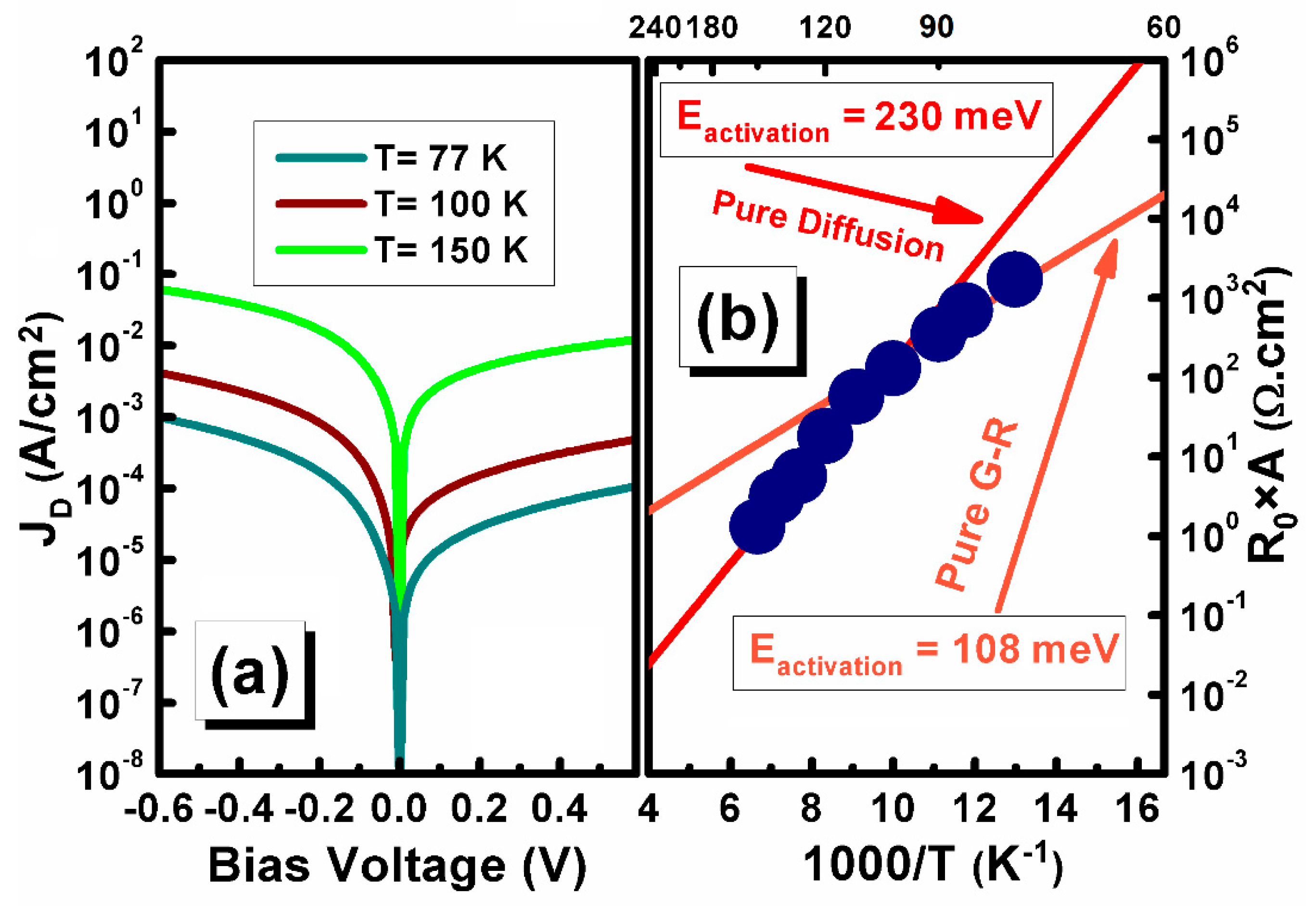
At Vb = +40 mV and T = 77 K, a 200 µm diameter optimized PT2SL device (IEng = 380 KeV and IDose = 1.0 × 1015 cm−2) shows the JD of 5.21 × 10⁻⁶ A/cm2. If the temperature is increased to 100 K the JD goes to 4.10 × 10⁻⁵ A/cm2. At 150 K, it increases to 2.68 × 10⁻³ A/cm2 (Figure 3a). An Arrhenius plot of the differential resistance area product at zero bias (R0 × A) indicates that the dark current is dominated by different mechanisms in different temperature regimes (Figure 3b). Above 100 K, the detector is diffusion limited with an activation energy (Eactivation) of 230 meV. This Eactivation is very close to the expected bandgap of the MWIR InAs/InAs1−xSbx superlattices in this temperature regime. From 100 to 77 K, the detector becomes generation-recombination limited with an Eactivation of 108 meV.
The devices were optically characterized under front–side–illumination (Figure 4) using a calibrated 1000 °C blackbody source along with a Fourier transform infrared (FTIR) spectrometer (Bruker IFS 66 v/S). No anti–refection (AR) coatings were applied to the device. The devices can operate unbiased, but it can still operate up to +40 mV before it gets saturated (Figure 4b). At 77 K and +40 mV bias, the 100% cut-off wavelength of the MWIR PT2SL device was 4.6 µm with a peak responsivity of 0.76 A/W at 3.8 µm, corresponding to a quantum efficiency (QE) of 21.5% (Figure 4a). At 150 K, the peak responsivity increases to 1.09 A/W, corresponding to a QE of 32.6%. These values are only slightly lower (17% lower at 150 k and 12% lower at 77 K) than those of the reference mesa-isolated device (Table 1). We speculate that this trend could be related to the optical contribution of the sloped mesa sidewalls in acting like mirrors and slightly enhancing the QE of mesa-isolated devices. It is worth noting that we tested the uniformity of the performances of the planar devices and the level of electrical isolation was not fully tested.
In order to ensure the ion-implantation is fully isolating, the diodes optical characterization of different size diodes was performed (Figure 4c). At all operating temperatures, the QE values are similar across a broad range of diode sizes (Figure 4c) and this is indicative that the ion-implantation is effective at defining the device active region and suggests this approach will scale down to pixel-size diodes and be a promising approach for FPA applications.
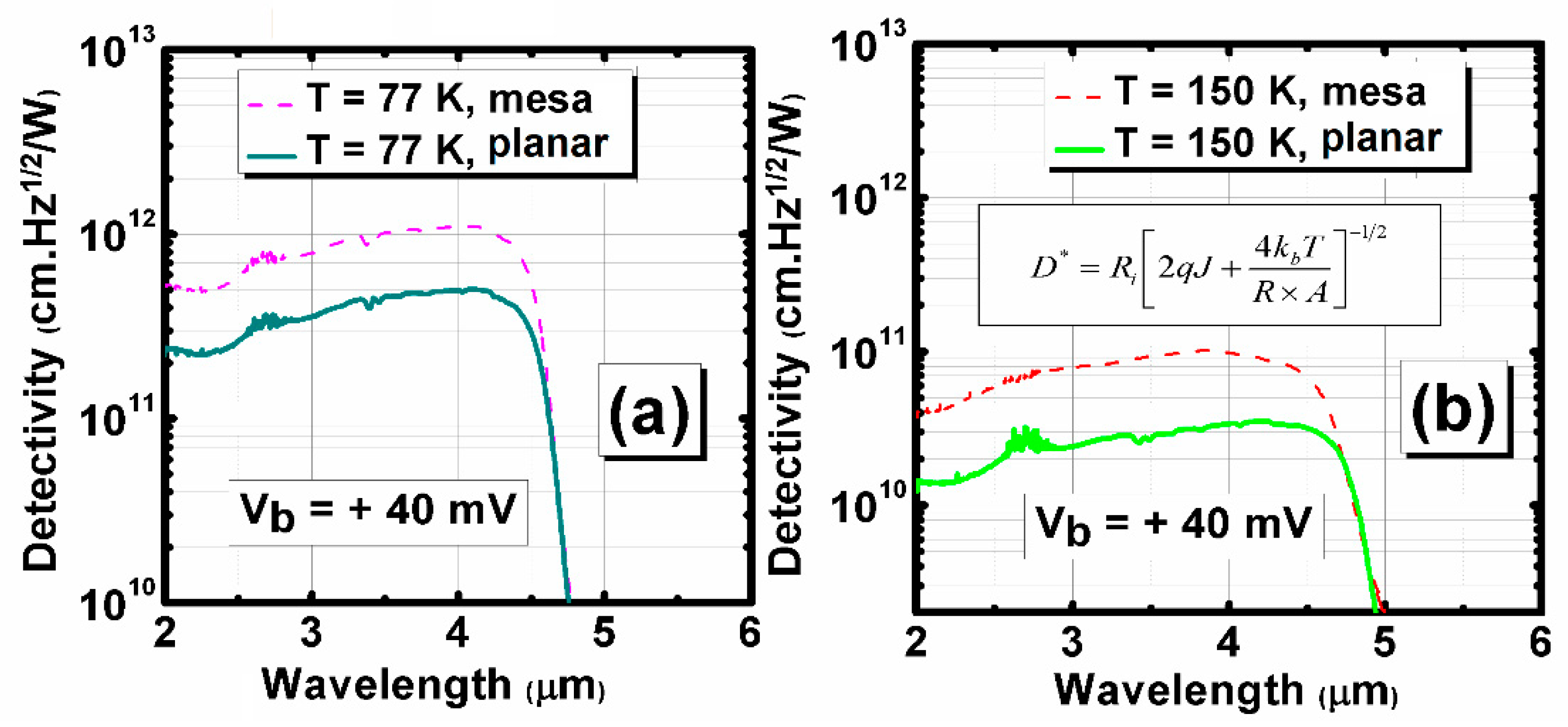
In order to estimate the detective performance of these novel planar devices in system applications, the specific detectivity (D*) was estimated assuming the device is shot noise-limited (Figure 5). At 150 K the planar device has a D* of ~3.37 × 1010 cm·Hz1/2/W at 3.8 μm, compared to ~1.0 × 1011 cm·Hz1/2/W for the mesa-isolated reference device. When the temperature is decreased to 77 K these D* values become even closer, with ~4.95 × 1011 cm·Hz1/2/W for planar device and ~1.10 × 1012 cm·Hz1/2/W for the mesa-isolated device. These detectivities are comparable to the mesa-isolated reference device and with further optimization of the ion-implantation process as well as refinement to the design of the structure, it should be possible to achieve parity in these 200 µm diameter devices and possibly superior performance in pixel-size devices that are currently dominated by mesa-sidewall leakage.
In summary, we have reported silicon ion-implanted planar pBn MWIR photodetectors based on type-II InAs/InAs1−xSbx superlattices. Several ion-implantation energies and doses were studied and the best performance was obtained with IEng = 380 KeV and IDose = 1.0 × 1015 cm−2. At 77 K, this optimized planar photodetector exhibits a peak responsivity of 0.76 A/W at 3.8 µm, corresponding to a quantum efficiency of 21.5% under Vb = +40 mV. With a 77 K dark current density of 5.21 × 10⁻⁶ A/cm2 at the same +40 mV of applied bias, the photodetector exhibits a specific detectivity of 4.95 × 1011 cm·Hz1/2/W. At 150 K, the optimized planar device’s dark current density increases to 2.68 × 10⁻³ A/cm2 and a detectivity drops to 3.37 × 1010 cm·Hz1/2/W.
Author Contributions
Conceptualization, A.D.; methodology, A.D.; validation, A.D. and R.M.; formal analysis, A.D.; investigation, A.D., D.W., J.L. and A.J.; resources, M.R. and D.W.; data curation, A.D; writing—original draft preparation, A.D.; writing—review and editing, A.D., R.M. and M.R.; supervision, M.R. All authors have read and agreed to the published version of the manuscript.
Funding
This material is based upon work supported by the Night Vision and Electronic Sensors Directorate under Contract No. W909MY19P0027.
Acknowledgments
The authors would like to acknowledge Meimei Tidrow and Lesslie Hutchinson from Army Night Vision Laboratory for her support and encouragement.
Conflicts of Interest
The authors declare no conflict of interest.
Data Availability Statements
The data that support the findings of this study are available from the corresponding author upon reasonable request.
References
- Petersen, C.R.; Møller, U.; Kubat, I.; Zhou, B.; Dupont, S.; Ramsay, J.; Benson, T.; Sujecki, S.; Abdel-Moneim, N.; Tang, Z.; et al. Mid-infrared supercontinuum covering the 1.4–13.3 μm molecular fingerprint region using ultra-high NA chalcogenide step-index fibre. Nat. Photonics 2014, 8, 830. [Google Scholar] [CrossRef]
- Seddon, A.B. A prospective for new mid-infrared medical endoscopy using chalcogenide glasses. Int. J. Appl. Glass Sci. 2011, 2, 177–191. [Google Scholar] [CrossRef]
- Wartewig, S.; Neubert, R.H.H. Pharmaceutical applications of Mid-IR and Raman spectroscopy. Adv. Drug Deliv. Rev. 2005, 57, 1144–1170. [Google Scholar] [CrossRef] [PubMed]
- Hackwell, J.A.; Warren, D.W.; Bongiovi, R.P.; Hansel, S.J.; Hayhurst, T.L.; Mabry, D.J.; Sivjee, M.G.; Skinner, J.W. LWIR/MWIR imaging hyperspectral sensor for airborne and ground-based remote sensing. In Proceedings of the International Symposium on Optical Science, Engineering, and Instrumentation, Denver, CO, USA, 4–9 August 1996; pp. 102–107. [Google Scholar]
- Razeghi, M.; Dehzangi, A.; Wu, D.; McClintock, R.; Zhang, Y.; Durlin, Q.; Li, J.; Meng, F. Antimonite-based gap-engineered type-II superlattice materials grown by MBE and MOCVD for the third generation of infrared imagers. In Proceedings of the Infrared Technology and Applications XLV, Baltimore, MD, USA, 14–18 April 2019; p. 110020G. [Google Scholar]
- Rogalski, A.; Martyniuk, P.; Kopytko, M. Type-II superlattice photodetectors versus HgCdTe photodiodes. Prog. Quantum Electron. 2019, 68, 100228. [Google Scholar] [CrossRef]
- Razeghi, M.; Haddadi, A.; Dehzangi, A.; Chevallier, R.; Yang, T. Recent advances in InAs/InAs1−xSbx/AlAs1−xSbx gap-engineered type-II superlattice-based photodetectors. In Proceedings of the SPIE Defense + Commercial Sensing, Anaheim, CA, USA, 9–13 April 2017; p. 1017705. [Google Scholar]
- Piotrowski, J.; Piotrowski, A. Mercury Cadmium Telluride: Growth, Properties and Applications; Wiley: Hoboken, NJ, USA, 2010; Room temperature IR photodetectors; pp. 513–537. [Google Scholar]
- Dehzangi, A.; Haddadi, A.; Adhikary, S.; Razeghi, M. Impact of scaling base thickness on the performance of heterojunction phototransistors. Nanotechnology 2017, 28, 10LT01. [Google Scholar] [CrossRef]
- Dehzangi, A.; McClintock, R.; Wu, D.; Li, J.; Johnson, S.M.; Dial, E.; Razeghi, M. High speed antimony-based superlattice photodetectors transferred on sapphire. Appl. Phys. Express 2019, 12, 116502. [Google Scholar] [CrossRef]
- Hoang, A.M.; Dehzangi, A.; Adhikary, S.; Razeghi, M. High performance bias-selectable three-color Short-wave/Mid-wave/Long-wave Infrared Photodetectors based on Type-II InAs/GaSb/AlSb superlattices. Sci. Rep. Artic. 2016, 6, 24144. [Google Scholar] [CrossRef] [Green Version]
- Nguyen, B.-M.; Hoffman, D.; Delaunay, P.-Y.; Huang, E.K.-W.; Razeghi, M.; Pellegrino, J. Band edge tunability of M-structure for heterojunction design in Sb based type II superlattice photodiodes. Appl. Phys. Lett. 2008, 93, 163502. [Google Scholar] [CrossRef]
- Binh-Minh, N.; Guanxi, C.; Minh-Anh, H.; Razeghi, M. Growth and Characterization of Long-Wavelength Infrared Type-II Superlattice Photodiodes on a 3-in GaSb Wafer. IEEE J. Quantum Electron. 2011, 47, 686–690. [Google Scholar] [CrossRef]
- Zegrya, G.G.; Andreev, A.D. Mechanism of suppression of Auger recombination processes in type-II heterostructures. Appl. Phys. Lett. 1995, 67, 2681–2683. [Google Scholar] [CrossRef]
- Dehzangi, A.; Haddadi, A.; Chevallier, R.; Zhang, Y.; Razeghi, M. Fabrication of 12 µm pixel-pitch 1280 × 1024 extended short wavelength infrared focal plane array using heterojunction type-II superlattice-based photodetectors. Semicond. Sci. Technol. 2019, 34, 03LT01. [Google Scholar] [CrossRef]
- Dehzangi, A.; Haddadi, A.; Chevallier, R.; Zhang, Y.; Razeghi, M. Bn extended short-wavelength infrared focal plane array. Opt. Lett. 2018, 43, 591–594. [Google Scholar] [CrossRef] [PubMed]
- Delaunay, P.-Y.; Hood, A.; Nguyen, B.M.; Hoffman, D.; Wei, Y.; Razeghi, M. Passivation of type-II InAs∕GaSb double heterostructure. Appl. Phys. Lett. 2007, 91, 091112. [Google Scholar] [CrossRef]
- Salihoglu, O.; Muti, A.; Aydinli, A. A comparative passivation study for InAs/GaSb pin superlattice photodetectors. IEEE J. Quantum Electron. 2013, 49, 661–666. [Google Scholar] [CrossRef] [Green Version]
- Rutkowski, J. Planar junction formation in HgCdTe infrared detectors. Opto-Electron. Rev. 2004, 12, 123–128. [Google Scholar]
- Musca, C.A.; Antoszewski, J.; Dell, J.M.; Faraone, L.; Terterian, S. Planar p-on-n HgCdTe heterojunction mid-wavelength infrared photodiodes formed using plasma-induced junction isolation. J. Electron. Mater. 2003, 32, 622–626. [Google Scholar] [CrossRef]
- Chang, S.-H.; Fang, Y.-K.; Ting, S.-F.; Chen, S.-F.; Lin, C.-Y.; Wu, C.-Y. Ultra high performance planar InGaAs PIN photodiodes for high speed optical fiber communication. Sens. Actuators A Phys. 2007, 133, 9–12. [Google Scholar] [CrossRef]
- Arias, J.M.; Arias, J.M.; Pasko, J.G.; Zandian, M.; Shin, S.H.; Williams, G.M.; Bubulac, L.O.; DeWames, R.E.; Tennant, W.E. Planar p-on-n HgCdTe heterostructure photovoltaic detectors. Appl. Phys. Lett. Appl. Phys. Lett. 1993, 62, 976. [Google Scholar] [CrossRef]
- Arias, J.; Pasko, J.G.; Zandian, M.; Shin, S.H.; Williams, G.M.; Bubulac, L.O.; de Wames, R.E.; Tennant, W.E. MBE HgCdTe heterostructure p-on-n planar infrared photodiodes. J. Electron. Mater. 1993, 22, 1049. [Google Scholar] [CrossRef]
- Zandian, M.; Scott, D.; Garnett, J.; Edwall, D.D.; Pasko, J.; Farris, M.; Daraselia, M.; Arias, J.M.; Bajaj, J.; Hall, D.N.B.; et al. Ten-inch molecular beam epitaxy production system for HgCdTe growth. J. Electron. Mater. 2005, 34, 891. [Google Scholar] [CrossRef]
- Wu, D.; Dehzangi, A.; Li, J.; Razeghi, M. High performance Zn-diffused planar mid-wavelength infrared type-II InAs/InAs1−xSbx superlattice photodetector by MOCVD. Appl. Phys. Lett. 2020, 116, 161108. [Google Scholar] [CrossRef] [Green Version]
- Pearton, S. Ion implantation for isolation of III-V semiconductors. J. Mater. Sci. Rep. 1990, 4, 313–363. [Google Scholar] [CrossRef]
- Eisen, F.H. Ion implantation in III–V compounds. Radiat. Eff. 1980, 47, 99–115. [Google Scholar] [CrossRef]
- Donnelly, J.P. The electrical characteristics of ion implanted compound semiconductors. Nucl. Instrum. Methods 1981, 182–183, 553–571. [Google Scholar] [CrossRef]
- Dehzangi, A.; Wu, D.; McClintock, R.; Li, J.; Razeghi, M. Planar nBn type-II superlattice mid-wavelength infrared photodetectors using zinc ion-implantation. Appl. Phys. Lett. 2020, 116, 221103. [Google Scholar] [CrossRef]
- Asano, T.; Atanassov, R.D.; Ishiwara, H.; Furukawa, S. Formation of Thick, Thermally-Stable High-Resistivity-Layers in GaAs by Oxygen Ion Implantation. Jpn. J. Appl. Phys. 1981, 20, 90107. [Google Scholar] [CrossRef]
- Ting, A.S.; Rafol, S.B.; Fisher, A.M.; Keo, S.A.; Khoshakhlagh, A.; Gunapala, S.D. Mid-wavelength infrared InAsSb/InAs nBn detectors and FPAs with very low dark current density. Appl. Phys. Lett. 2019, 114, 161103. [Google Scholar]
- Haddadi, A.; Dehzangi, A.; Chevallier, R.; Adhikary, S.; Razeghi, M. Bias-selectable nBn dual-band long-/very long-wavelength infrared photodetectors based on InAs/InAs1−xSbx/AlAs1−xSbx type-II superlattices. Sci. Rep. 2017, 7, 3379. [Google Scholar] [CrossRef] [Green Version]
- Wu, D.; Dehzangi, A.; Razeghi, M. Demonstration of mid-wavelength infrared nBn photodetectors based on type-II InAs/InAs1−xSbx superlattice grown by metal-organic chemical vapor deposition. Appl. Phys. Lett. 2019, 115, 061102. [Google Scholar] [CrossRef]
- Chevallier, R.; Dehzangi, A.; Haddadii, A.; Razeghi, M. Type-II superlattice-based extended short-wavelength infrared focal plane array with an AlAsSb/GaSb superlattice etch-stop layer to allow near-visible light detection. Opt. Lett. 2017, 42, 4299. [Google Scholar] [CrossRef]
- Dehzangi, A.; McClintock, R.; Haddadi, A.; Wu, D.; Chevallier, R.; Razeghi, M. Type-II superlattices base visible/extended short–wavelength infrared photodetectors with a bandstructure-engineered photo-generated carrier extractor. Sci. Rep. 2019, 9, 5003. [Google Scholar] [CrossRef] [PubMed] [Green Version]
Figure 1.
Images of the planar type-II superlattice (PT2SL) photodetector at different processing steps: (a) Scanning electron microscope (SEM) image and (b) optical micrograph of a circular diode covered by hard mask, ready for implantation, (c) optical micrograph after window opening to the top metal contact, and (d) SEM image after wire bonding, ready for test. (e) Schematic diagram of the device structure where the arrows showing the area of ion-implantation to isolate the diodes.

Figure 2.
(a) JD values vs. temperature for mid-wavelength infrared (MWIR) PT2SL photodetectors with IEng of 380 KeV and different IDose. (b) JD values vs. temperature with IDose = 1.0 × 1015 cm−2 and different IEng. All diodes were circular with a 200 μm diameter and the applied bias (Vb) is +40 mV.

Figure 3.
(a) JD vs. bias voltage at different temperatures for the pBn planar photodetector processed with IEng = 380 KeV and IDose = 1.0 × 1015 cm−2. (b) Arrhenius plot of the R0×A. Solid lines represent linear fits of the two dominate regimes.
Figure 3.
(a) JD vs. bias voltage at different temperatures for the pBn planar photodetector processed with IEng = 380 KeV and IDose = 1.0 × 1015 cm−2. (b) Arrhenius plot of the R0×A. Solid lines represent linear fits of the two dominate regimes.

Figure 4.
(a) Saturated 77 K and 150 K quantum efficiency (QE) spectra of the 200 µm diameter optimized planar device compared to a reference mesa-isolated device. The 100% cut-off wavelength is 4.6 µm at 77 K and increases to 4.9 µm at 150 K; (b) responsivity vs. bias voltage showing saturation at +40 mV; and (c) QE vs. diameter showing no size dependence.

Figure 5.
(a) Specific detectivity (D*) spectrum for the optimized planar (IEng = 300 KeV and Idose = 1.0 × 1015 cm−2) and mesa-isolated MWIR T2SL photodetectors at (a) 77 K and (b) 150 K. Calculation is based on the shot noise limited detectivity equation in the inset where q is the charge of the electron, kb is Boltzmann’s constant, J is the dark current density at the applied bias (Vb) of +40 mV, R × A is the differential resistance area product at Vb = +40 mV, Ri is the spectral responsivity, and T is the temperature.


Table 1.
Comparison of the QE of the planar and mesa-isolated type-II superlattice (T2SL) devices at 150 and 77 K at λ = 3.8 μm and at the applied bias of +40 mV.
Table 1.
Comparison of the QE of the planar and mesa-isolated type-II superlattice (T2SL) devices at 150 and 77 K at λ = 3.8 μm and at the applied bias of +40 mV.
| Device. | QE 150K | QE 77K |
|---|---|---|
| mesa | 39.2% | 24.4% |
| Planar | 32.6% | 21.5% |
© 2020 by the authors. Licensee MDPI, Basel, Switzerland. This article is an open access article distributed under the terms and conditions of the Creative Commons Attribution (CC BY) license (http://creativecommons.org/licenses/by/4.0/).
Share and Cite
MDPI and ACS Style
Dehzangi, A.; Wu, D.; McClintock, R.; Li, J.; Jaud, A.; Razeghi, M. Demonstration of Planar Type-II Superlattice-Based Photodetectors Using Silicon Ion-Implantation. Photonics 2020, 7, 68. https://doi.org/10.3390/photonics7030068
AMA Style
Dehzangi A, Wu D, McClintock R, Li J, Jaud A, Razeghi M. Demonstration of Planar Type-II Superlattice-Based Photodetectors Using Silicon Ion-Implantation. Photonics. 2020; 7(3):68. https://doi.org/10.3390/photonics7030068
Chicago/Turabian StyleDehzangi, Arash, Donghai Wu, Ryan McClintock, Jiakai Li, Alexander Jaud, and Manijeh Razeghi. 2020. "Demonstration of Planar Type-II Superlattice-Based Photodetectors Using Silicon Ion-Implantation" Photonics 7, no. 3: 68. https://doi.org/10.3390/photonics7030068
Note that from the first issue of 2016, this journal uses article numbers instead of page numbers. See further details here.