Tunable Plasmonic Perfect Absorber for Hot Electron Photodetection in Gold-Coated Silicon Nanopillars
by
 , and
, and
Tangyou Sun
1,2 ,
,
Wenke Song
1,
Zubin Qin
1,
Wenjing Guo
1,
Peihua Wangyang
1,2,*,
Zhiping Zhou
3 and
Yanrong Deng
1,* 1
Guangxi Key Laboratory of Precision Navigation Technology and Application, Guilin University of Electronic Technology, Guilin 541004, China
2
Key Laboratory of Microelectronic Devices and Integrated Circuits, Education Department of Guangxi Zhuang Autonomous Region, Guilin University of Electronic Technology, Guilin 541004, China
3
State Key Laboratory of Advanced Optical Communication Systems and Networks, School of Electronics Engineering and Computer Science, Peking University, Beijing 100871, China
*
Authors to whom correspondence should be addressed.
Photonics 2023, 10(1), 60; https://doi.org/10.3390/photonics10010060
Submission received: 6 December 2022
/
Revised: 20 December 2022
/
Accepted: 22 December 2022
/
Published: 6 January 2023
(This article belongs to the Special Issue Mid-Infrared Integrated Photonics)
Abstract
:Infrared detection technology has important applications in laser ranging, imaging, night vision, and other fields. Furthermore, recent studies have proven that hot carriers which are generated by surface plasmon decay can be exploited for photodetection to get beyond semiconductors’ bandgap restriction. In this study, silicon nanopillars (NPs) and gold film at the top and bottom of silicon nanopillars were designed to generate surface plasmon resonance and Fabry–Perot resonance to achieve perfect absorption. The absorption was calculated using the Finite Difference Time Domain (FDTD) method, and factors’ effects on resonance wavelength and absorption were examined. Here we demonstrate how this perfect absorber can be used to achieve near-unity optical absorption using ultrathin plasmonic nanostructures with thicknesses of 15 nm, smaller than the hot electron diffusion length. Further study revealed that the resonance wavelength can be redshifted to the mid-infrared band (e.g., 3.75 μm) by increasing the value of the structure parameters. These results demonstrate a success in the study of polarization insensitivity, detection band adjustable, and efficient perfect absorption infrared photodetectors.
1. Introduction
Infrared photodetection has been widely used for telecommunication [1,2], imaging [3], surveillance [4], and military purposes. Common photodetectors are mainly based on the mechanisms of photoconductance, photovoltaic, and so on. One type of photogenerated carrier is captured by the defect state, etc., in a photoconductance device, while the other is cycled through the device’s channel multiple times through being pushed by an electric field to add photoconductance gain. Higher photoconductance gains can be achieved by extending the lifetime of a few carriers or by using channel materials with high mobility. However, the response of photoconductance components is generally slow, in the order of ms to s. The detector based on the photo-volt effect relies on the electric field built in the junction to separate the photogenerated electron–hole pair and generate the photogenerated potential difference or photogenerated current. Photovoltaic detectors usually have a fast response speed, but due to the lack of a gain mechanism, the responsiveness of the device is not high. Photoconductance and photovoltaic devices are usually limited by the bandgap of semiconductor materials [5]. In recent years, surface plasmon has attracted much attention because the hot electrons can be transferred quickly and photoelectric conversion can be realized.
Surface Plasmons (SPs), coherent oscillations of free electrons in metal nanostructures that can excite with electromagnetic waves, provide a novel means of enhancing light–matter interaction at the nanoscale [6,7,8]. SPs can generally be divided into two classes: Localized Surface Plasmon Polariton (LSPP) (also commonly referred to as Surface Plasmons Resonance, SPR), residing on metal nanoparticles (approximately zero-dimensional structure), and Propagating Surface Plasmon Polariton (PSPP), which exists at the metal–dielectric interface. The electromagnetic field of surface plasmons is localized in a region much smaller than the wavelength scale. The energy of incident light will converge in deep subwavelength or even nanoscale space through SPs, which can greatly enhance the energy density and local electric field intensity of light, forming hot spots [9]. Following excitation, plasmons undergo non-radiative relaxation, during the electron collective oscillation process. Then, electron–electron collisions (time scales of 10 to 100 fs) lead to the de-coherence of the plasmons. The energy of the plasmons is converted to quantized electrons by the excitation of in-band electron transitions (sp band) and inter-band electron transitions (d band–sp band) [10,11]. This process produces highly energetic electrons, also known as “hot electrons”, which can escape from the plasmonic nanostructures, then over-stride the metal-semiconductor Schottky junction. Finally, hot electrons will be collected by the electrode. Therefore, SPs can significantly enhance the interaction between light and matter. Due to the strong local constraint of SPs, the light field and energy are limited to the sub-wavelength scale. Thanks to state-of-the-art fabrication techniques such as electron-beam (EBL) and focused ion-beam (FIB), as well as commercially available numerical design tools like FDTD, in addition to research on self-assembled nanostructures [12,13], the design and fabrication of metallic nanostructures for infrared range has now become very effective. It shows great potential applications such as subwavelength light confinement within ultra-small mode volume [14], ultra-compact lens and waveplates [15,16], ultrasensitive sensing [17,18], hot carrier generation for photodetection and photochemistry [19,20,21,22,23,24], etc. Among them, the hot electrons produced by SPR excitation can be transferred rapidly and photoelectric transfer can be realized. In this case, the response wavelength of the device is determined by the contact barrier between the materials rather than the band gap of the semiconductor. This working mode breaks the bottleneck that the response band of the traditional detector is limited by the semiconductor band gap, so it has a great advantage in the field of infrared detection. The electromagnetic field localization caused by the plasmon resonance effect can also significantly enhance the light absorption of the material [25] and improve the photoelectric conversion efficiency. However, the main drawbacks of previously demonstrated hot electron detectors are their low photoresponsivity [26,27] and poor light absorption [28,29]. Recent studies report significant advances in detector efficiency and absorption efficiency by exciting propagating SPP using metal gratings [30] or combining gratings with deep trench cavities [31]. Therefore, plasmonic grating is a widely studied nanostructure that can achieve hot electron detection, but polarization dependence and extra bandwidth response are unexpected.
In this study, we have designed a hot-electron perfect absorption photodetector based on Au/Si-NPs arrays/Au, which is capable of photodetection in the near-infrared range. We can attain polarization angle insensitivity as a result of this. Our Schottky diode-based hot-electron photodetectors have great photoresponsivity in the near-infrared region, which is below the Si energy gap, thanks to the ideal absorber integrated with n-Si. The stable and efficient absorption was achieved by adjusting the structural parameters of the Si-NPs arrays. The SPs generated by Au/Si-NPs arrays and Fabry–Perot resonance generated by the top and bottom gold film effectively improved the optical absorption efficiency. Specifically, by studying the relationship between the parameters of the perfect absorber and resonant wavelength, we realized the detection in the mid-infrared range.
2. Structure Design and Simulation Model
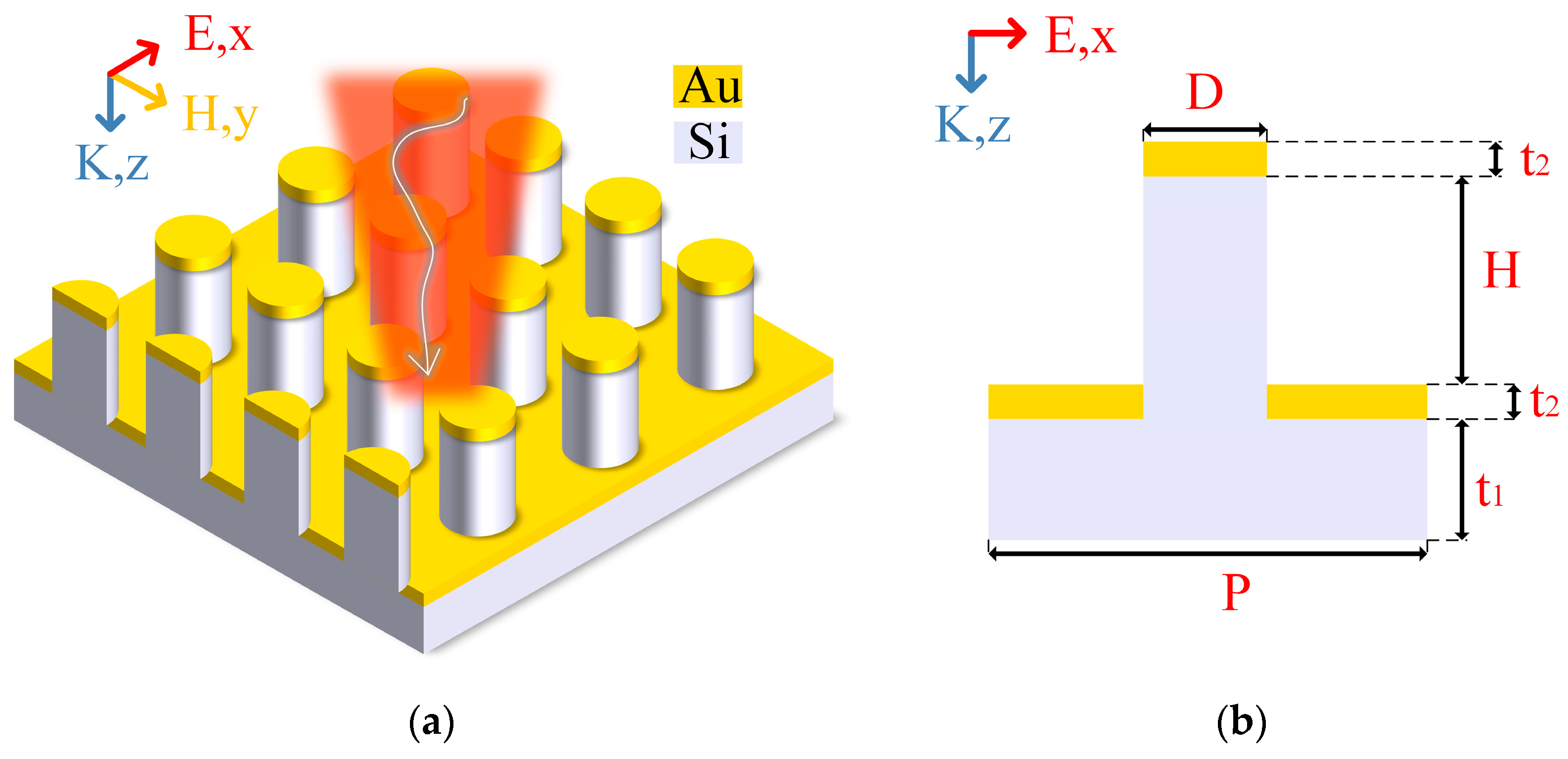
Figure 1a shows the schematic of our perfect absorption photodetectors, which consist of n-type Si NPs arrays substrate, forming a 2D optical grating, with a 15 nm gold film deposited on the surface and bottom. As shown in Figure 1b, the metal film is naturally separated into top and bottom plasmonic stripe resonators. Orthogonally arranged Si NPs covered with metal are used to excite a strong electric field, which can boost hot carrier generation [26]. Importantly, the thickness of the plasmonic resonator is only 15 nm, less than the electron diffusion length [32], ensuring that the hot carrier has a high probability of diffusing to the metal–semiconductor interface. The 3D finite-difference time-domain (FDTD) simulation is performed using commercial software (Lumerical FDTD Solutions 2020 R2) to investigate the optical properties of the proposed structure. A Three-Dimensional (3D) simulation model was built based on the FDTD method to study the Perfect Photodetectors Absorption property for the dependency of Si NP of height, diameter, and period. The periodic boundary conditions were adopted for a unit cell in both x and y directions, and the perfectly matched layers (PML) were applied in the z condition to eliminate the interference of double scattering. In the structure of gold, we used discrete mesh with a size of 5 × 5 × 2 nm3. In order to ensure the convergence of simulation results, the simulation time is set to 3000 fs. FDTD simulations were performed using the experimental dielectric function from Palik [33] for the gold and silicon materials. The incident source is a linearly polarized plane wave (1100 nm–2000 nm) propagating along the negative Z direction with the E field polarization to the X direction.
3. Result and Discussions
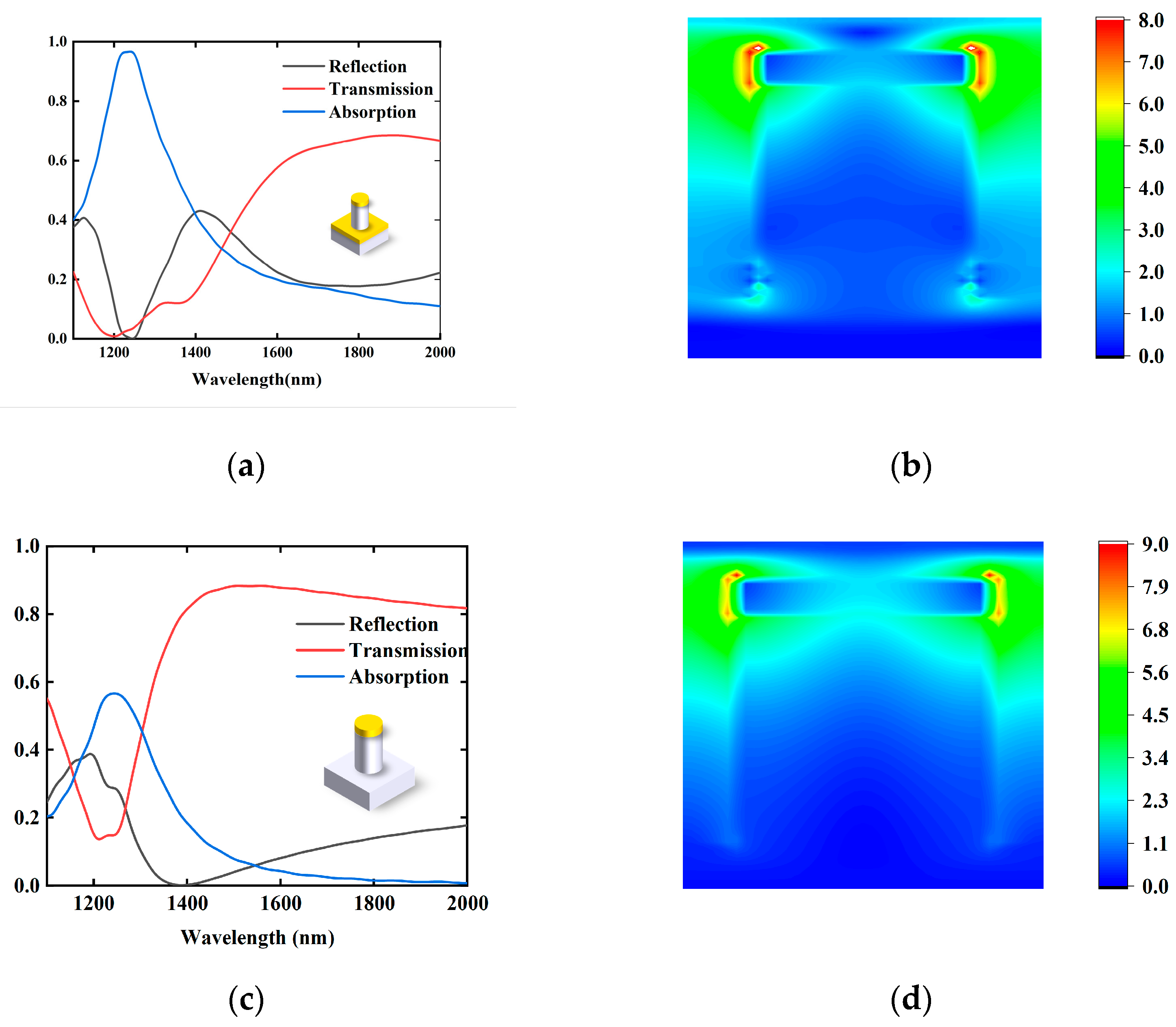
The FDTD method was used to investigate the optical absorption of the structure of Au/Si NP arrays/Au. Two monitors were used to calculate the reflection (R) coefficient and transmission (T) coefficient during the simulation. Furthermore, the absorption (A) coefficient can be calculated by A = 1-R-T. As shown in Figure 2a, it is seen that a broadband optical absorption in the near-infrared region has a maximum value of ~96% and a FWHM of ~1785 nm. We did not further tweak the parameters to bring the optical absorption close to one, as we focused more on the research of the law of change. The physical origin of perfect absorption is the interaction of propagating SPR, LSPR, and Fabry–Perot resonance [34]. Another approach is the anti-reflection of nanostructures [35] to increase optical absorption. To characterize the hot-electron response, Figure 2b shows the electric-field intensity distribution at the X-Z section at the wavelength (1285 nm) with the highest absorption. In the X-Z section, this structure can be known as Au/silicon/Au “sandwich” nanostructure. Qianyi Shangguan et al. [36] proposed an ultra-narrow band graphene refractive index sensor, consisting of a patterned graphene layer on the top, a dielectric layer of SiO2 in the middle, and a bottom Au layer. They achieved absorption efficiency of the absorption sensor of 99.41% and 99.22% at 5.664 THz and 8.062 THz by exciting the plasma of graphene. It can become conscious of two-part local enhancement effects. One of the biggest electric fields is around the bottom corner of the gold film, because the gold attached to the Si NP arrays can generate SPs [37].
Brongersma et al. [10] describe the photoexcitation and relaxation of metallic NP arrays with a four-step model. In this model, based on the law of conversion of electromagnetic energy, which is also called Poynting’s theorem [38], Jiaming Hao et al. [39] studied the losses associated with light passing through a medium, in which both the dielectric permittivity and magnetic permeability are dispersive and absorptive. In their research, the time-averaged dissipative energy density in the case of the magnetically dispersive medium can be written as:
where represents the incident light frequency, represents the imaginary part of the metal permittivity, and represents the local electric field. Therefore, Equation (1) shows that the absorption intensity is proportional to the square of the total electric field amplitude [40]. Another local enhancement effect electric field presents to the bottom of Si NP, which is caused by a Fabry–Perot resonance. Compared with the no-bottom gold film structure in Figure 2c,d, this structure does not have the bottom enhancement effect. Additionally, it has lower absorption than the first structure. Hence, gold arrays and Fabry–Perot resonance have optical coupling, so that the structure with top and bottom gold film can show higher absorption.
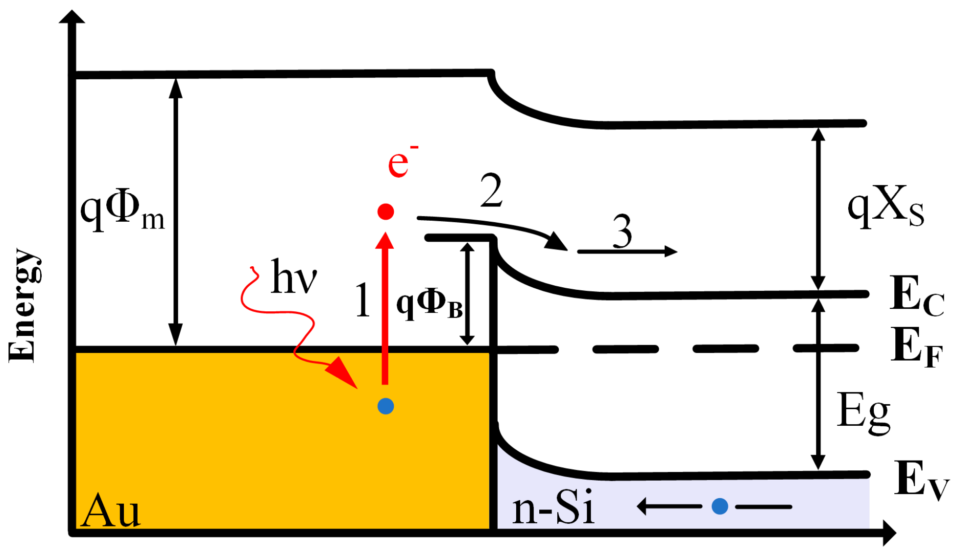
Enhancing the absorption is the first step to achieving photoelectric detection. The structure of Au/Si NP arrays/Au can realize the high optical absorption based on gold arrays and Fabry–Perot resonance optical coupling. There are three steps where the light current collected from the optical absorption to the electrodes, as shown in Figure 3, step (1) corresponds to hot electron generation. The plasmonic field can cause electrons to move from occupied to unoccupied by causing plasmons to non-radiatively decay into hot electrons (optical absorption). The distribution of hot carriers is then influenced by the shape of Si NP, the electronic structure, and other factors. In most cases, the spatial distribution of hot carrier generation from photon absorption can be written as:
where the is the resistive loss of absorbed photon energy, which is dissipated without hot electron generation arising from the finite carrier lifetime. Step (2) Diffusion to the Schottky interface. Hot electrons transport to the metal–semiconductor interface before thermalization; Wang et al. used a typical metal–insulator–metal (MIM) structure to achieve a strong chiral effect in hot carrier generation, and the hot electron excitation is considered as a surface quantum effect formalism from carrier scatting by the metal surface [21]:
where is the potential barrier height, is the component of the electric field normal to the surface, taken inside metal, and the integral is taken over the metal surface. Step (3) Transmission to the conduction band of the semiconductor: hot electrons injected into the conduction band of the semiconductor through internal photoemission. The hot carrier injection efficiency is a crucial factor to determine device performance, which is described as the number of electrons with sufficient energy to overcome the barrier [26]:
where is the Flower emission coefficient, is the photo energy, and is the Schottky barrier energy height between gold and silicon. In our work, we simulated the distributions of electric fields for two different structures. According to Equations (1)–(4), we can describe the contribution of optical absorption to the hot carrier by its electric field.
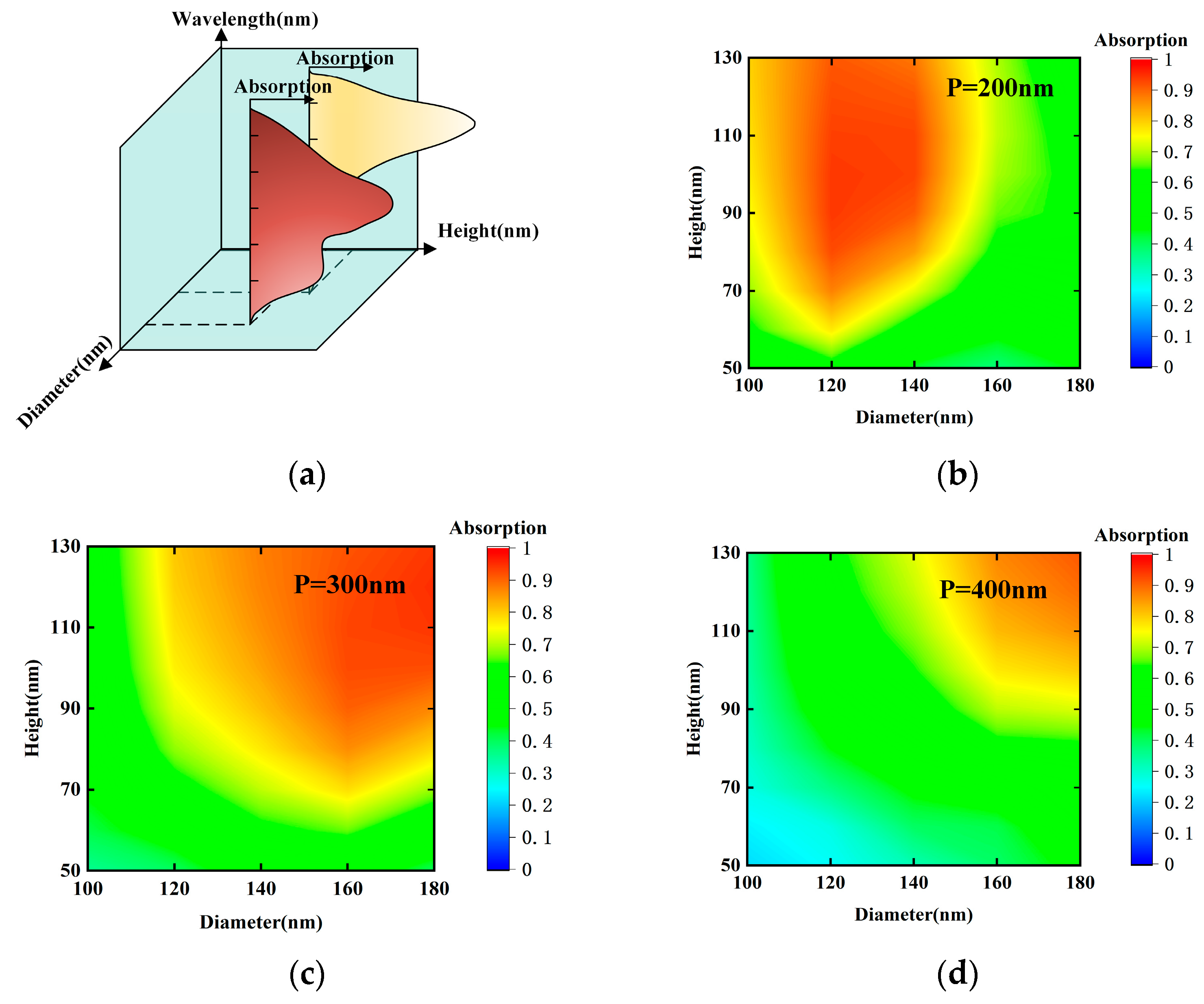
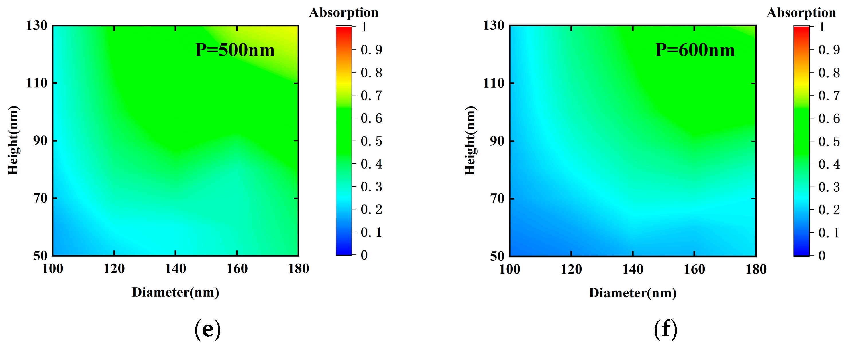
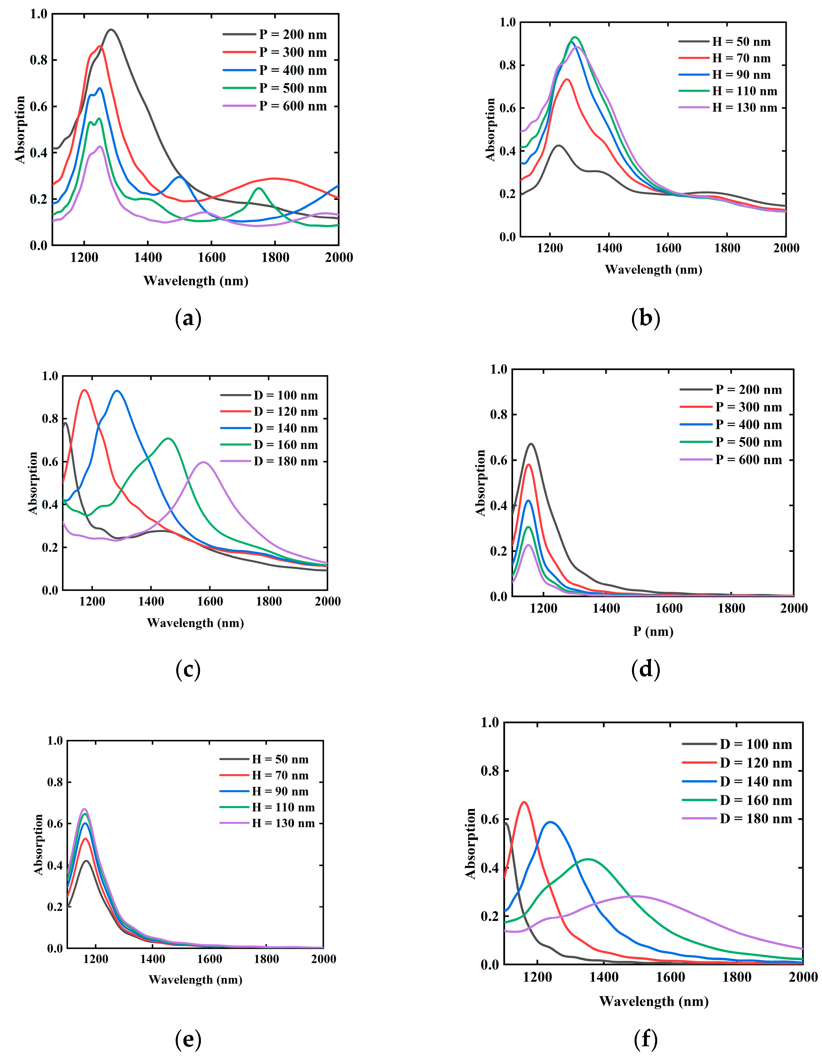
To intuitively know the effects of Si nanostructures on optical absorption, the relationships between structure parameters and the optical absorption were obtained by changing the period (P), height (H), and radius (R) of the Si nanoarrays. Firstly, absorption curves were plotted in a 3D system of coordinates, shown in Figure 4a. It cannot clearly show the change rule. The relationships between structure characteristics with different periods and the maximum absorption are therefore shown using a much simplified method. Figure 4b–f displays the simulated absorption spectra with the period of Si arrays increasing from 200 nm to 600 nm, the radius increasing from 50 nm to 90 nm, and the height increasing from 50 nm to 130 nm, respectively. It is intuitively seen that the absorption coefficient is decreased and the highest absorption peaks present greater height and radius values as the p value increases. Meanwhile, absorption efficiencies at resonance wavelengths apparently decline, which depends on the weaker plasmonic resonances in the structure of Au/Si NP arrays/Au. More specifically, either a larger period or a smaller radius makes a wider gap between the gold films above the Si NPs, which weakens the magnetic dipole resonance.
In the previous part, we researched the relationships between structure parameters and the highest optical absorption coefficient. In addition, it is meaningful to examine the influence of the period, height, and radius of Si NPs on the absorption spectrum. Figure 5a–c shows the absorption of Au/Si NP arrays/Au with fixed height H = 0.11 μm, D = 0.12 μm, and various period P, fixed diameter D = 0.12 μm, period P = 0.2 μm, and various height H, fixed height H = 0.11 μm, period P = 0.2 μm, and various diameter D, respectively. Analogously, we used the same method where two parameters were fixed and the remaining one was changed to observe the influence of parameter change on the absorption of Au/Si NP arrays; the result is shown in Figure 5d–f. To obtain the relationship between the absorption wavelength and parameters of the Si NP arrays, the absorption wavelength can be obtained by using the SPP dispersion equation, which is shown as below [41]:
where is the wave-vector in a vacuum, is the relative permittivity of the dielectric, and is the dielectric function of the metal which can be described by the Drude model. When the periodical NPs are introduced, the SPP wavevector is expressed as [42]:
where is the horizontal angle of the incident wave vector, is the grating period, and is an integer. From Equation (6), it can be seen that absorption wavelength depends only on the horizontal dimension rather than the [43] vertical dimension [44]. The horizontal dimension includes period and diameter. Firstly, the period mainly affects the density of the NP arrays for constant diameter data. When the periodicity increased from 200 nm to 600 nm, the average absorptivity decreased by 54.2%; the result is shown in Figure 5a. The absorption decreased with an increase in periodicity because the area ratio of the Si NP arrays was reduced. As shown in Figure 5d, structures without gold at the bottom also show the same pattern. The height H of Si NP also influenced the absorption, as shown in Figure 5b,e. For the structure of Au/Si NP arrays/Au with an increase in H, the absorptivity between 50 and 130 nm increased slightly. Additionally, the absorption peak showed a small redshift with increasing Si NP height. Compared with the structure of Au/Si NP arrays, there is no redshift. Therefore, the resonance wavelength is redshifted by the Fabry–Perot resonator. The distinct feature of SPR, as can be observed in Figure 5c, is that the absorption peak results from the SPR and the resonant wavelength of the absorption peak redshifts as the diameter of the Si pillars increases. Compared with Figure 5f, the structure without gold at the bottom also shows the same pattern.
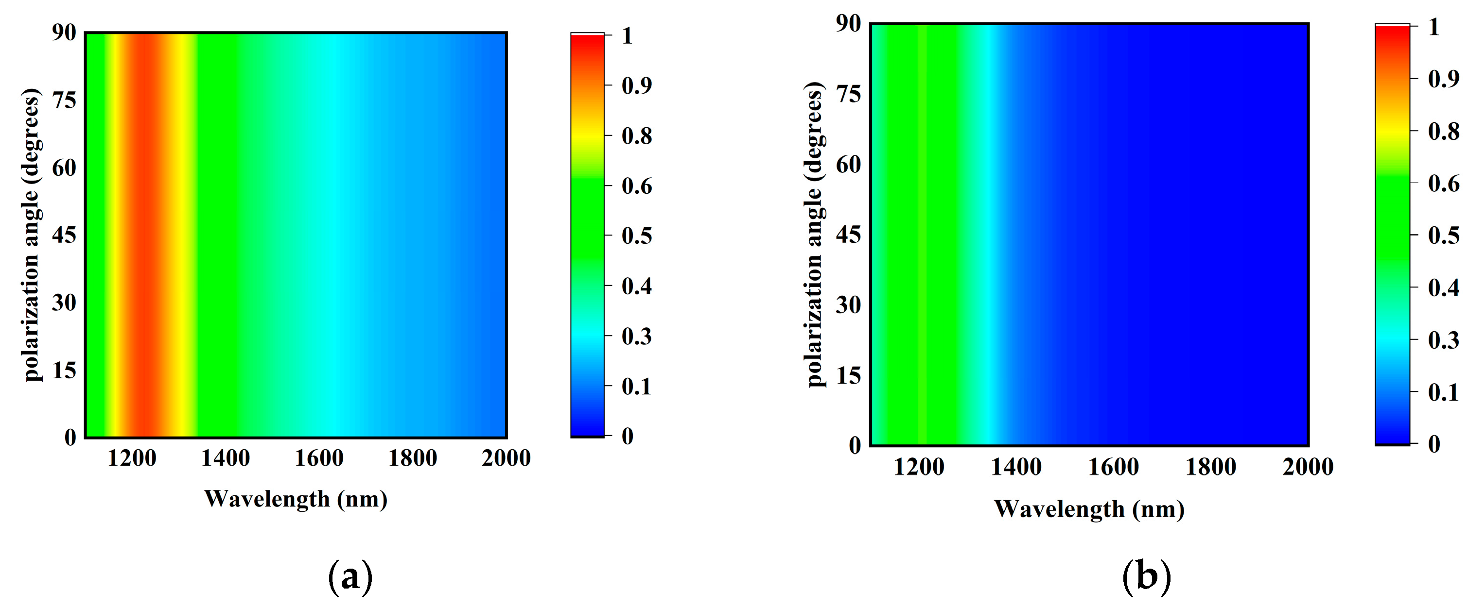
The polarization dependence of the designed perfect absorption photodetectors is also numerically investigated. As shown in Figure 6a,b, the structure with and without metal at the bottom is absorbed in a polarization angle of 0–90 degrees, respectively. A polarization angle equal to zero means that polarization direction is along the x direction (TE polarization), and equal to 90 means that polarization is along the y direction (TM polarization). Unsurprisingly, the absorber has the same resonance wavelengths under 0–90 polarization degrees at normal incidence due to the symmetrical arrangement of Si NP arrays. Polarization independence means the stable absorption of the absorber [45]. Therefore, the absorber that shows polarization independence has more application potential.
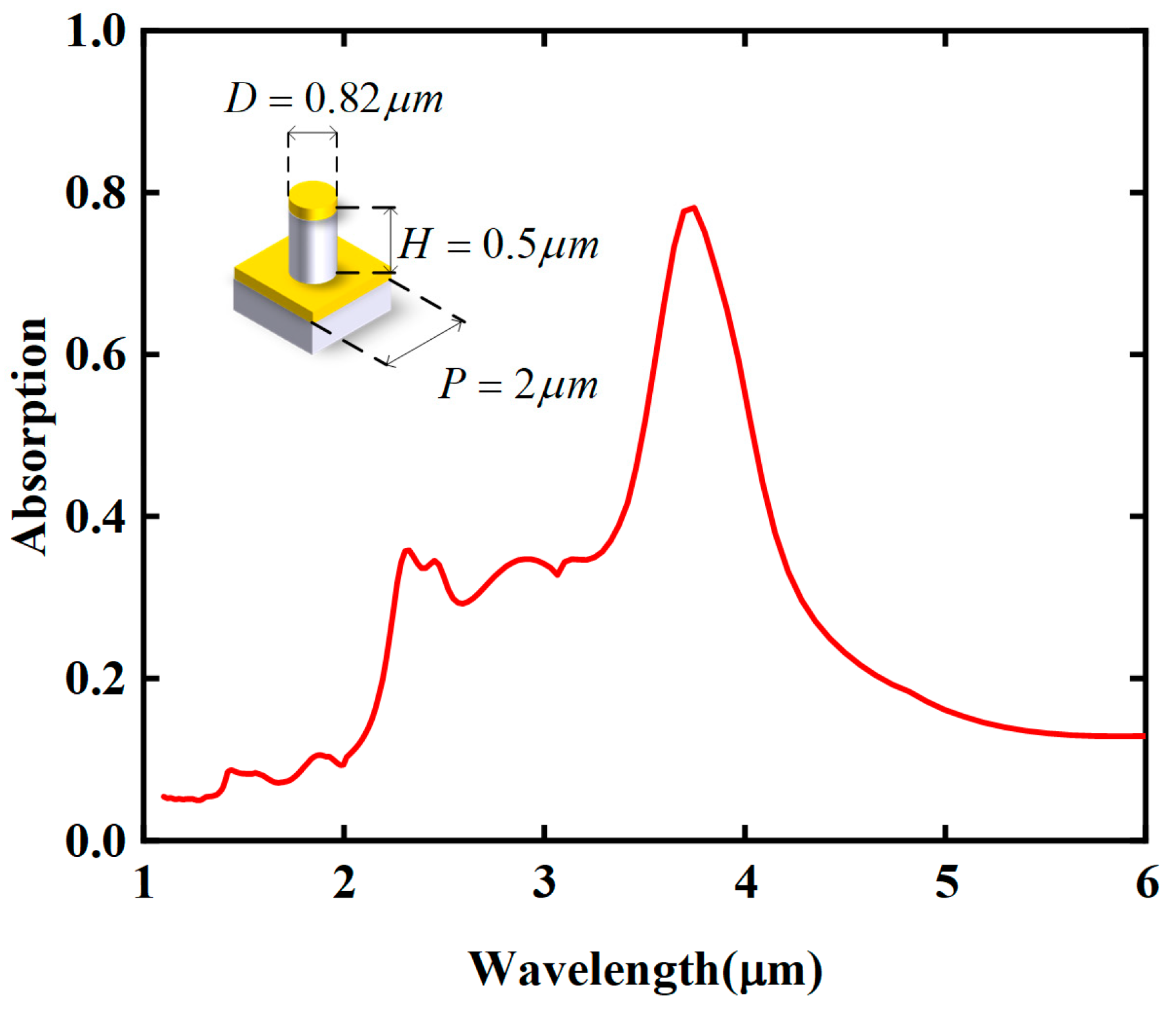
Taking advantage of the high photoresponsivity and tunability of the structure Au/Si-NPs arrays/Au, we can further achieve mid-infrared photodetection. Based on previous studies in the near-infrared range, we understand the parameter dependence and polarization dependence of the perfect absorption photodetectors. It is known that the resonant wavelength of the absorption peak redshifts as the diameter of the Si pillars increases. Next, we try to use larger structural parameters to make the resonant wavelength move to the mid-infrared band. The result is shown in Figure 7; with the thickness of the gold constant, the radius, period, and height increase so that the resonant wavelength moves to 3.75 μm; meanwhile, optical absorption in the mid-infrared region has a maximum value of ~80%. Based on the previous research results, we did not optimize the absorption peak parameters of the mid-infrared band and still maintained absorptivity over 80%. It is intuitively seen that the resonant absorption peak is redshifted as D, P, and H values increase, which is related to the weaker plasmonic resonances in Au/Si-NPs arrays/Au. Therefore, by adjusting the structural parameters, the perfect absorber can work in the mid-infrared band.
In addition, metamaterials present intriguing strategies for active tuning and provide flat, high-efficiency alternatives to conventional optical systems based on bulky components [46]. Xingyu Wang et al. [47] proposed a tunable sensing detector based on Bulk Dirac semimetals (BDS); the result achieved three perfect absorption peaks with absorptivity greater than 99.8% in the range of 2.4–5.2 THz.
4. Conclusions
In summary, we have designed and prepared a hot-electron photodetector based on Au/Si NP arrays/Au structure, which can operate in the near-infrared range well below the Si bandgap energy. Realizing near-unity absorption within ultrathin plasmonic nanostructures, it allows the efficiency of the hot electron transfer process to be significantly enhanced. Therefore, the Au-Si Schottky architecture allows us to preserve a broadband, polarization invariant, resonance wavelength adjustable absorber. This ultra-compact, CMOS-compatible Si-based photoelectric detection can also be readily integrated into on-chip optoelectronics and can be scaled to the solar spectrum, leading to enhanced efficiencies in hot-electron-based photodetection, photovoltaic, and photocatalysis systems.
Author Contributions
Conceptualization, T.S. and W.S.; methodology, W.G.; software, Z.Q.; validation, T.S., P.W. and Y.D.; data curation, Z.Q. and Z.Z.; writing—original draft preparation, W.S.; writing—review and editing, T.S. and W.S. All authors have read and agreed to the published version of the manuscript.
Funding
This research was funded by National Natural Science Foundation of China (61805053), Guangxi Science and Technology Project (No. AD18281030), Natural Science Foundation of Guangxi Province (2018GXNSFBA281152), Guangxi Key Laboratory of Precision Navigation Technology and Application, Guilin University of Electronic Technology (No. DH202203, No. DH202205), Innovation Project of GUET Graduate Education (2022YCXS043). Project was supported by Guangxi Key Laboratory of Precision Navigation Technology and Application, Guilin University of Electronic Technology (No. DH202205).
Institutional Review Board Statement
Not applicable.
Informed Consent Statement
Not applicable.
Data Availability Statement
The data that support the findings of this study are available from the corresponding author upon reasonable request.
Acknowledgments
The authors are grateful for the technical support from the School of Information and Communication, Guilin University of Electronic Technology.
Conflicts of Interest
The authors declare no conflict of interest.
References
- Goykhman, I.; Desiatov, B.; Khurgin, J.; Shappir, J.; Levy, U. Waveguide based compact silicon Schottky photodetector with enhanced responsivity in the telecom spectral band. Opt. Express 2012, 20, 28594–28602. [Google Scholar] [CrossRef] [PubMed]
- Goykhman, I.; Desiatov, B.; Khurgin, J.; Shappir, J.; Levy, U. Locally Oxidized Silicon Surface-Plasmon Schottky Detector for Telecom Regime. Nano Lett. 2011, 11, 2219–2224. [Google Scholar] [CrossRef] [PubMed]
- Engel, M.; Steiner, M.; Avouris, P. Black Phosphorus Photodetector for Multispectral, High-Resolution Imaging. Nano Lett. 2014, 14, 6414–6417. [Google Scholar] [CrossRef]
- Gong, X.; Tong, M.; Xia, Y.; Cai, W.; Moon, J.S.; Cao, Y.; Yu, G.; Shieh, C.-L.; Nilsson, B.; Heeger, A.J. High-Detectivity Polymer Photodetectors with Spectral Response from 300 nm to 1450 nm. Science 2009, 325, 1665–1667. [Google Scholar] [CrossRef]
- Zhu, Y.; Xu, H.; Yu, P.; Wang, Z. Engineering plasmonic hot carrier dynamics toward efficient photodetection. Appl. Phys. Rev. 2021, 8, 021305. [Google Scholar] [CrossRef]
- Schuller, J.A.; Barnard, E.S.; Cai, W.; Jun, Y.C.; White, J.S.; Brongersma, M.L. Plasmonics for extreme light concentration and manipulation. Nat. Mater. 2010, 9, 368. [Google Scholar] [CrossRef]
- Gramotnev, D.K.; Bozhevolnyi, S.I. Plasmonics beyond the diffraction limit. Nat. Photonics 2010, 4, 83–91. [Google Scholar] [CrossRef]
- Epstein, I.; Alcaraz, D.; Huang, Z.; Pusapati, V.-V.; Hugonin, J.-P.; Kumar, A.; Deputy, X.M.; Khodkov, T.; Rappoport, T.G.; Hong, J.-Y.; et al. Far-field excitation of single graphene plasmon cavities with ultracompressed mode volumes. Science 2020, 368, 1219–1223. [Google Scholar] [CrossRef]
- Hou, W.; Cronin, S.B. A Review of Surface Plasmon Resonance-Enhanced Photocatalysis. Adv. Funct. Mater. 2013, 23, 1612–1619. [Google Scholar] [CrossRef]
- Brongersma, M.L.; Halas, N.J.; Nordlander, P. Plasmon-induced hot carrier science and technology. Nat. Nanotechnol. 2015, 10, 25–34. [Google Scholar] [CrossRef]
- Hartland, G.V.; Besteiro, L.V.; Johns, P.; Govorov, A.O. What’s so hot about electrons in metal nanoparticles? ACS Energy Lett. 2017, 2, 1641–1653. [Google Scholar] [CrossRef] [Green Version]
- Liu, W.; Li, Q.; Wu, J.; Wang, W.; Jiang, R.; Zhou, C.; Wang, S.; Zhang, X.; Sun, T.; Xu, Z.; et al. Self-assembly of Au nanocrystals into large-area 3-D ordered flexible superlattice nanostructures arrays for ultrasensitive trace multi-hazard detection. J. Hazard. Mater. 2023, 443, 130124. [Google Scholar] [CrossRef] [PubMed]
- Li, H.; Cao, L.; Fu, T.; Li, Q.; Zhang, F.; Xiao, G.; Chen, Y.; Liu, X.; Zhao, W.; Yu, Z.; et al. Morphology-dependent high antireflective surfaces via anodic aluminum oxide nanostructures. Appl. Surf. Sci. 2019, 496, 143697. [Google Scholar] [CrossRef]
- Baumberg, J.J.; Aizpurua, J.; Mikkelsen, M.H.; Smith, D.R. Extreme nanophotonics from ultrathin metallic gaps. Nat. Mater. 2019, 18, 668–678. [Google Scholar] [CrossRef] [PubMed]
- Fang, N.; Lee, H.; Sun, C.; Zhang, X. Sub-Diffraction-Limited Optical Imaging with a Silver Superlens. Science 2005, 308, 534–537. [Google Scholar] [CrossRef] [Green Version]
- Yu, N.; Capasso, F. Flat optics with designer metasurfaces. Nat. Mater. 2014, 13, 139–150. [Google Scholar] [CrossRef]
- Coppens, Z.J.; Li, W.; Walker, D.G.; Valentine, J.G. Probing and Controlling Photothermal Heat Generation in Plasmonic Nanostructures. Nano Lett. 2013, 13, 1023–1028. [Google Scholar] [CrossRef] [Green Version]
- Zhang, S.; Bao, K.; Halas, N.J.; Xu, H.; Nordlander, P. Substrate-Induced Fano Resonances of a Plasmonic Nanocube: A Route to Increased-Sensitivity Localized Surface Plasmon Resonance Sensors Revealed. Nano Lett. 2011, 11, 1657–1663. [Google Scholar] [CrossRef]
- Li, W.; Valentine, J.G. Harvesting the loss: Surface plasmon-based hot electron photodetection. Nanophotonics 2017, 6, 177–191. [Google Scholar] [CrossRef]
- Reddy, H.; Wang, K.; Kudyshev, Z.; Zhu, L.; Yan, S.; Vezzoli, A.; Higgins, S.J.; Gavini, V.; Boltasseva, A.; Reddy, P.; et al. Determining plasmonic hot-carrier energy distributions via single-molecule transport measurements. Science 2020, 369, 423–426. [Google Scholar] [CrossRef]
- Wang, W.; Besteiro, L.V.; Liu, T.; Wu, C.; Sun, J.; Yu, P.; Chang, L.; Wang, Z.M.; Govorov, A.O. Generation of Hot Electrons with Chiral Metamaterial Perfect Absorbers: Giant Optical Chirality for Polarization-Sensitive Photochemistry. ACS Photonics 2019, 6, 3241–3252. [Google Scholar] [CrossRef]
- Besteiro, L.V.; Yu, P.; Wang, Z.; Holleitner, A.W.; Hartland, G.V.; Wiederrecht, G.P.; Govorov, A.O. The fast and the furious: Ultrafast hot electrons in plasmonic metastructures. Size and structure matter. Nano Today 2019, 27, 120–145. [Google Scholar] [CrossRef]
- Khorashad, L.K.; Besteiro, L.V.; Correa-Duarte, M.A.; Burger, S.; Wang, Z.M.; Govorov, A.O. Hot Electrons Generated in Chiral Plasmonic Nanocrystals as a Mechanism for Surface Photochemistry and Chiral Growth. J. Am. Chem. Soc. 2020, 142, 4193–4205. [Google Scholar] [CrossRef] [PubMed]
- Liu, T.; Besteiro, L.V.; Liedl, T.; Correa-Duarte, M.A.; Wang, Z.; Govorov, A.O. Chiral Plasmonic Nanocrystals for Generation of Hot Electrons: Toward Polarization-Sensitive Photochemistry. Nano Lett. 2019, 19, 1395–1407. [Google Scholar] [CrossRef] [Green Version]
- Ni, Z.; Ma, L.; Du, S.; Xu, Y.; Yuan, M.; Fang, H.; Wang, Z.; Xu, M.; Li, D.; Yang, J.; et al. Plasmonic Silicon Quantum Dots Enabled High-Sensitivity Ultrabroadband Photodetection of Graphene-Based Hybrid Phototransistors. ACS Nano 2017, 11, 9854–9862. [Google Scholar] [CrossRef]
- Knight, M.W.; Sobhani, H.; Nordlander, P.; Halas, N.J. Photodetection with Active Optical Antennas. Science 2011, 332, 702–704. [Google Scholar] [CrossRef]
- Knight, M.W.; Wang, Y.; Urban, A.S.; Sobhani, A.; Zheng, B.Y.; Nordlander, P.; Halas, N.J. Embedding Plasmonic Nanostructure Diodes Enhances Hot Electron Emission. Nano Lett. 2013, 13, 1687–1692. [Google Scholar] [CrossRef]
- Scales, C.; Berini, P. Thin-Film Schottky Barrier Photodetector Models. IEEE J. Quantum Electron. 2010, 46, 633–643. [Google Scholar] [CrossRef]
- Manjavacas, A.; Liu, J.G.; Kulkarni, V.; Nordlander, P. Plasmon-Induced Hot Carriers in Metallic Nanoparticles. ACS Nano 2014, 8, 7630–7638. [Google Scholar] [CrossRef]
- Sobhani, A.; Knight, M.; Wang, Y.; Zheng, B.; King, N.S.; Brown, L.V.; Fang, Z.; Nordlander, P.; Halas, N. Narrowband photodetection in the near-infrared with a plasmon-induced hot electron device. Nat. Commun. 2013, 4, 1643. [Google Scholar] [CrossRef]
- Lin, K.-T.; Chen, H.-L.; Lai, Y.-S.; Yu, C.-C. Silicon-based broadband antenna for high responsivity and polarization-insensitive photodetection at telecommunication wavelengths. Nat. Commun. 2014, 5, 3288. [Google Scholar] [CrossRef] [PubMed] [Green Version]
- Sze, S.; Moll, J.; Sugano, T. Range-energy relation of hot electrons in gold. Solid-State Electron. 1964, 7, 509–523. [Google Scholar] [CrossRef]
- Palik, E.D. Handbook of Optical Constants of Solids; Elsevier: Amsterdam, The Netherlands, 1998. [Google Scholar]
- Gao, H.; Peng, W.; Liang, Y.; Chu, S.; Yu, L.; Liu, Z.; Zhang, Y. Plasmonic Broadband Perfect Absorber for Visible Light Solar Cells Application. Plasmonics 2019, 15, 573–580. [Google Scholar] [CrossRef]
- Sun, T.; Liu, Y.; Tu, J.; Zhou, Z.; Cao, L.; Liu, X.; Li, H.; Li, Q.; Fu, T.; Zhang, F.; et al. Wafer-scale high anti-reflective nano/micro hybrid interface structures via aluminum grain dependent self-organization. Mater. Des. 2020, 194, 108960. [Google Scholar] [CrossRef]
- Shangguan, Q.; Chen, Z.; Yang, H.; Cheng, S.; Yang, W.; Yi, Z.; Wu, X.; Wang, S.; Yi, Y.; Wu, P. Design of Ultra-Narrow Band Graphene Refractive Index Sensor. Sensors 2022, 22, 6483. [Google Scholar] [CrossRef] [PubMed]
- Qiu, S.; Tobing, L.Y.M.; Tong, J.; Xie, Y.; Xu, Z.; Ni, P.; Zhang, D.-H. Two-dimensional metallic square-hole array for enhancement of mid-wavelength infrared photodetection. Opt. Quantum Electron. 2016, 48, 203. [Google Scholar] [CrossRef]
- Jackson, J.D.; Fox, R.F. Classical Electrodynamics, 3rd ed. Am. J. Phys. 1999, 67, 841–842. [Google Scholar] [CrossRef]
- Hao, J.; Zhou, L.; Qiu, M. Nearly total absorption of light and heat generation by plasmonic metamaterials. Phys. Rev. B 2011, 83, 165107. [Google Scholar] [CrossRef]
- Loudon, R. The propagation of electromagnetic energy through an absorbing dielectric. J. Phys. A Gen. Phys. 1970, 3, 233. [Google Scholar] [CrossRef]
- Maier, S.A. Plasmonics: Fundamentals and Applications; Springer Science & Business Media: New York, NY, USA, 2007; Volume 1. [Google Scholar]
- Seddon, A.B. Mid-infrared (IR)—A hot topic: The potential for using mid-IR light for non-invasive early detection of skin cancer in vivo. Phys. Status Solidi (B) 2013, 250, 1020–1027. [Google Scholar] [CrossRef]
- Jackson, J.D. Classical Electrodynamics; American Association of Physics Teachers: College Park, MD, USA, 1999. [Google Scholar]
- Liu, Y.; Huang, W.; Gong, T.; Su, Y.; Zhang, H.; He, Y.; Liu, Z.; Yu, B. Ultra-sensitive near-infrared graphene photodetectors with nanopillar antennas. Nanoscale 2017, 9, 17459–17464. [Google Scholar] [CrossRef] [PubMed]
- Malheiros-Silveira, G.N.; Bhattacharya, I.; Deshpande, S.V.; Skuridina, D.; Lu, F.; Chang-Hasnain, C.J. Room-temperature Fabry-Perot resonances in suspended InGaAs/InP quantum-well nanopillars on a silicon substrate. Opt. Express 2017, 25, 271–277. [Google Scholar] [CrossRef] [PubMed]
- Xiao, S.; Wang, T.; Liu, T.; Zhou, C.; Jiang, X.; Zhang, J. Active metamaterials and metadevices: A review. J. Phys. D Appl. Phys. 2020, 53, 503002. [Google Scholar] [CrossRef]
- Wang, X.; Lin, J.; Yan, Z.; Yi, Z.; Yu, J.; Zhang, W.; Qin, F.; Wu, X.; Zhang, J.; Wu, P. Tunable high-sensitivity sensing detector based on Bulk Dirac semimetal. RSC Adv. 2022, 12, 32583–32591. [Google Scholar] [CrossRef] [PubMed]
Figure 1.
(a) Schematic of the proposed Au/Si NP arrays/Au perfect absorption photodetector. (b) The structure parameters are t1 = 1 μm, t2 = 0.015 μm, H = 0.12 μm, D = 0.13 μm, and P = 0.2 μm.
Figure 1.
(a) Schematic of the proposed Au/Si NP arrays/Au perfect absorption photodetector. (b) The structure parameters are t1 = 1 μm, t2 = 0.015 μm, H = 0.12 μm, D = 0.13 μm, and P = 0.2 μm.

Figure 2.
(a) Simulated optical reflection, transmission, and absorption for Au/Si NP arrays/Au. (b) Simulated electric field distribution in the structure of (a). (c) Simulated optical reflection, transmission, and absorption for Au/Si NP arrays. (d) Simulated electric field distribution in the structure of (c).

Figure 3.
Schematic of the hot electron transfer process over the Schottky barrier formed by the metal-semiconductor interface. Steps 1 to 3 correspond to hot electron generation, diffusion to the Schottky interface, and transmission to the conduction band of the semiconductor.
Figure 3.
Schematic of the hot electron transfer process over the Schottky barrier formed by the metal-semiconductor interface. Steps 1 to 3 correspond to hot electron generation, diffusion to the Schottky interface, and transmission to the conduction band of the semiconductor.

Figure 4.
(a) Schematic diagram of the three-dimensional relationship between absorption and radius, height, and wavelength. Si under the period of (b) 0.2 μm, (c) 0.3 μm, (d) 0.4 μm, (e) 0.5 μm, and (f) 0.6 μm. Height ranges from 0.05 μm to 0.13 μm with a step size of 0.02 μm. The radius factor ranges from 0.05 μm to 0.09 μm with a step size of 0.01 μm.


Figure 5.
(a–c) Calculated absorption spectra of the Au/Si NP arrays/Au with a varying period, height, and diameter, respectively. (d–f) Calculated absorption spectra of the Au/Si NP arrays with varying periods, heights, and diameters, respectively.
Figure 5.
(a–c) Calculated absorption spectra of the Au/Si NP arrays/Au with a varying period, height, and diameter, respectively. (d–f) Calculated absorption spectra of the Au/Si NP arrays with varying periods, heights, and diameters, respectively.

Figure 6.
The polarization angle dependence for (a) the structure of Au/Si NP arrays/Au and (b) the structure of Au/Si NP arrays.
Figure 6.
The polarization angle dependence for (a) the structure of Au/Si NP arrays/Au and (b) the structure of Au/Si NP arrays.

Figure 7.
Simulated optical absorption for Au/Si NP arrays/Au. The structure parameters are t1 = 1 μm, t2 = 0.015 μm, H = 0.5 μm, D = 0.82 μm, and P = 2 μm.
Figure 7.
Simulated optical absorption for Au/Si NP arrays/Au. The structure parameters are t1 = 1 μm, t2 = 0.015 μm, H = 0.5 μm, D = 0.82 μm, and P = 2 μm.

Disclaimer/Publisher’s Note: The statements, opinions and data contained in all publications are solely those of the individual author(s) and contributor(s) and not of MDPI and/or the editor(s). MDPI and/or the editor(s) disclaim responsibility for any injury to people or property resulting from any ideas, methods, instructions or products referred to in the content. |
© 2023 by the authors. Licensee MDPI, Basel, Switzerland. This article is an open access article distributed under the terms and conditions of the Creative Commons Attribution (CC BY) license (https://creativecommons.org/licenses/by/4.0/).
Share and Cite
MDPI and ACS Style
Sun, T.; Song, W.; Qin, Z.; Guo, W.; Wangyang, P.; Zhou, Z.; Deng, Y. Tunable Plasmonic Perfect Absorber for Hot Electron Photodetection in Gold-Coated Silicon Nanopillars. Photonics 2023, 10, 60. https://doi.org/10.3390/photonics10010060
AMA Style
Sun T, Song W, Qin Z, Guo W, Wangyang P, Zhou Z, Deng Y. Tunable Plasmonic Perfect Absorber for Hot Electron Photodetection in Gold-Coated Silicon Nanopillars. Photonics. 2023; 10(1):60. https://doi.org/10.3390/photonics10010060
Chicago/Turabian StyleSun, Tangyou, Wenke Song, Zubin Qin, Wenjing Guo, Peihua Wangyang, Zhiping Zhou, and Yanrong Deng. 2023. "Tunable Plasmonic Perfect Absorber for Hot Electron Photodetection in Gold-Coated Silicon Nanopillars" Photonics 10, no. 1: 60. https://doi.org/10.3390/photonics10010060
Note that from the first issue of 2016, this journal uses article numbers instead of page numbers. See further details here.