
On-Chip Modification of Titanium Electrothermal Characteristics by Joule Heating: Application to Terahertz Microbolometer

 , ,
, ,
Abstract
:1. Introduction
- (1)
- Crystalline defects, such as vacancy, interstitial, dislocation, etc., to be reduced, resulting in lower resistivity and TCR closer to that of bulk material.
- (2)
- Grain size increase, also resulting in lower resistivity and TCR closer to that of bulk material. This may alleviate the narrow width effect caused by the small grain size.
- (3)
- Phase separation in the case of multi-element material, i.e., where impurities are included unintentionally.
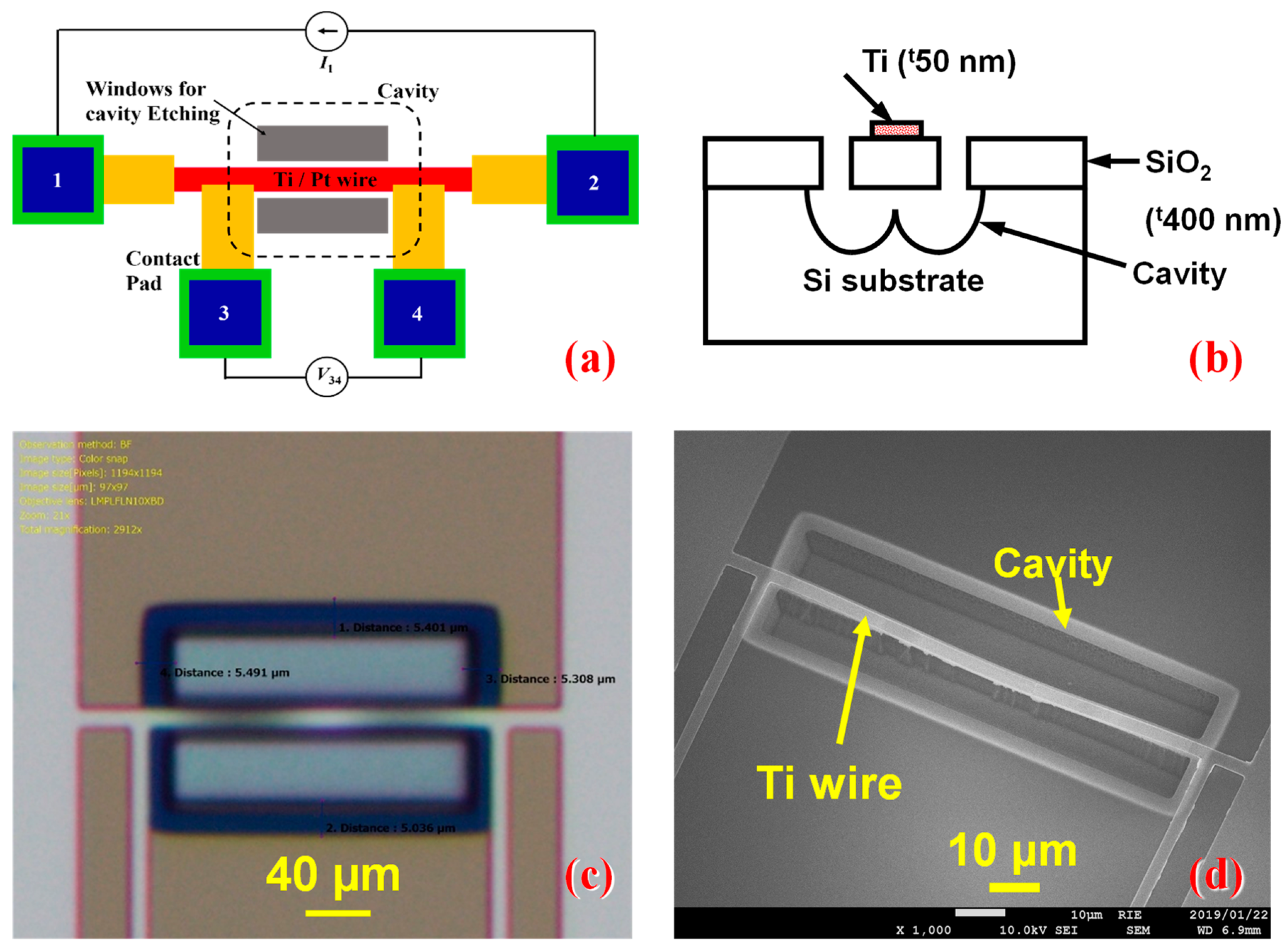
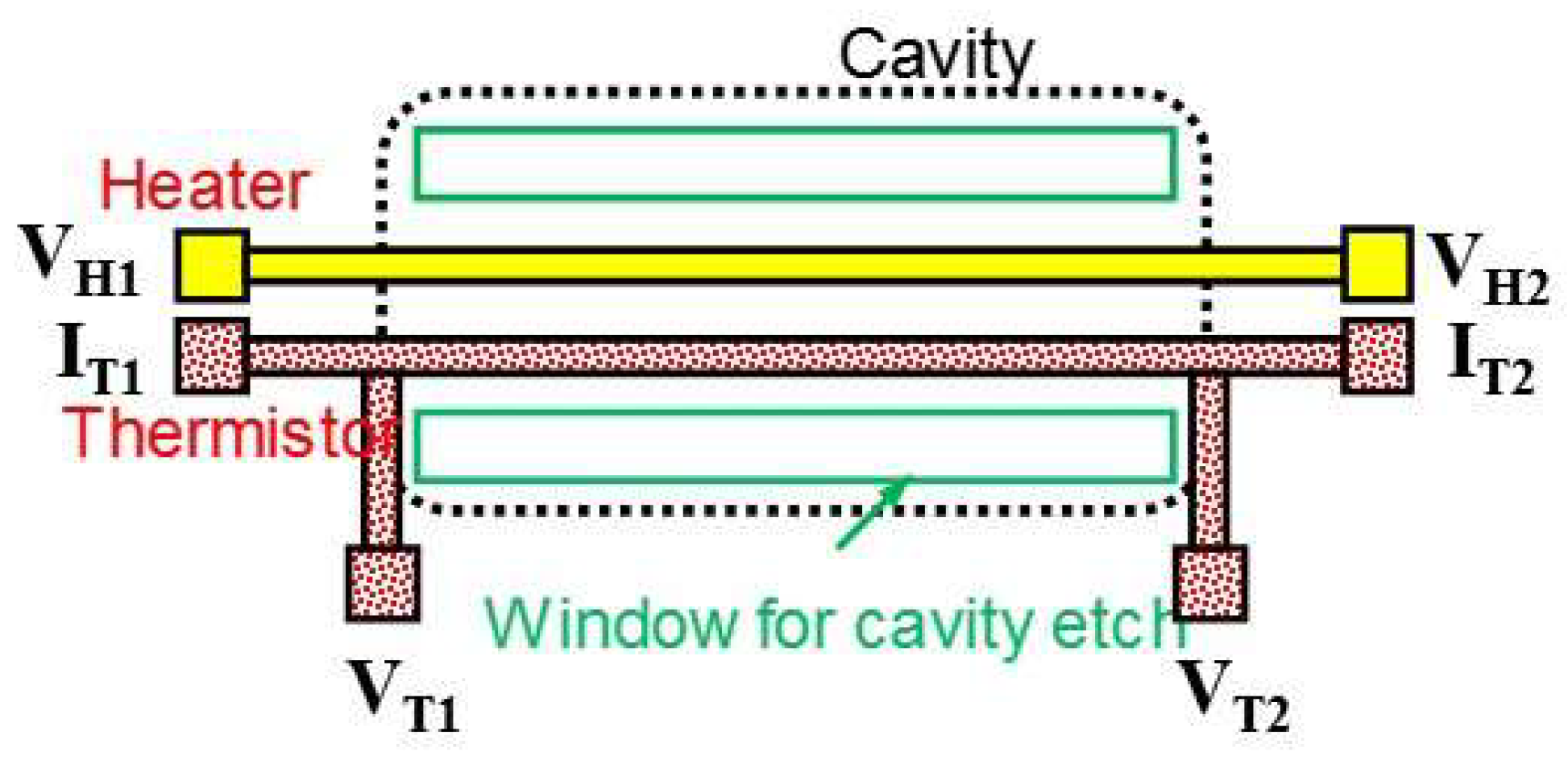
2. Materials and Methods
3. Results and Discussion
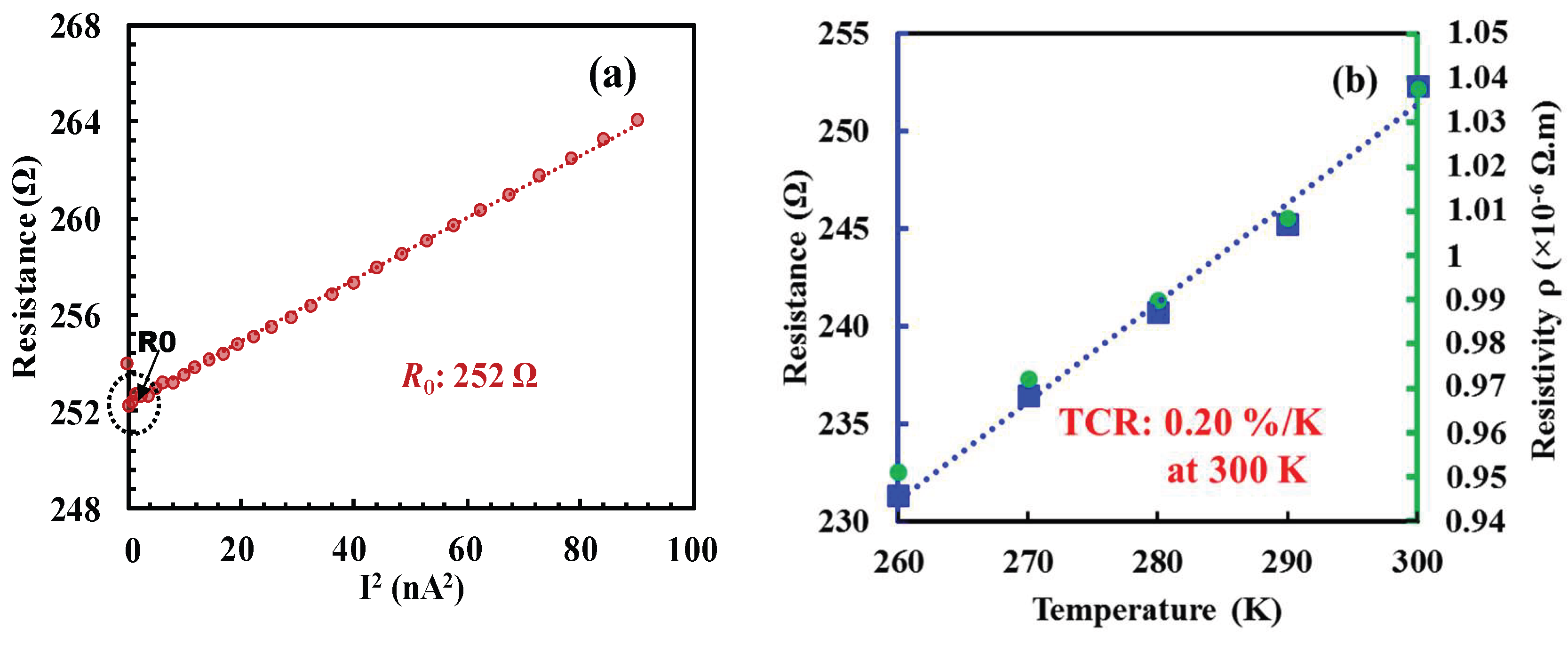
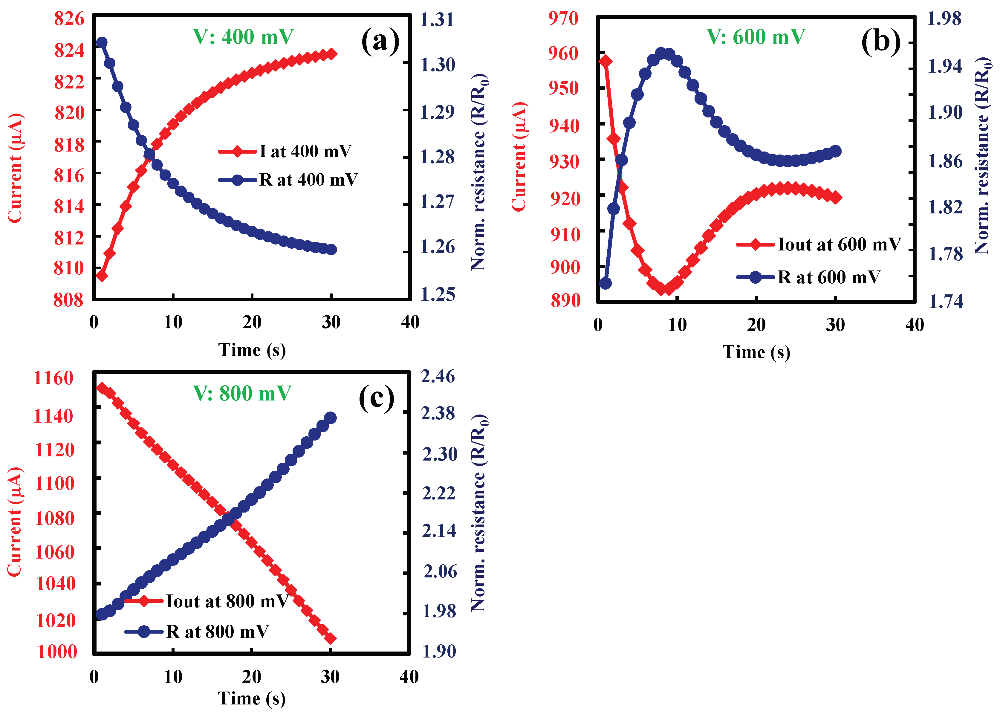
3.1. Comparative Study: Before and after Joule Heating
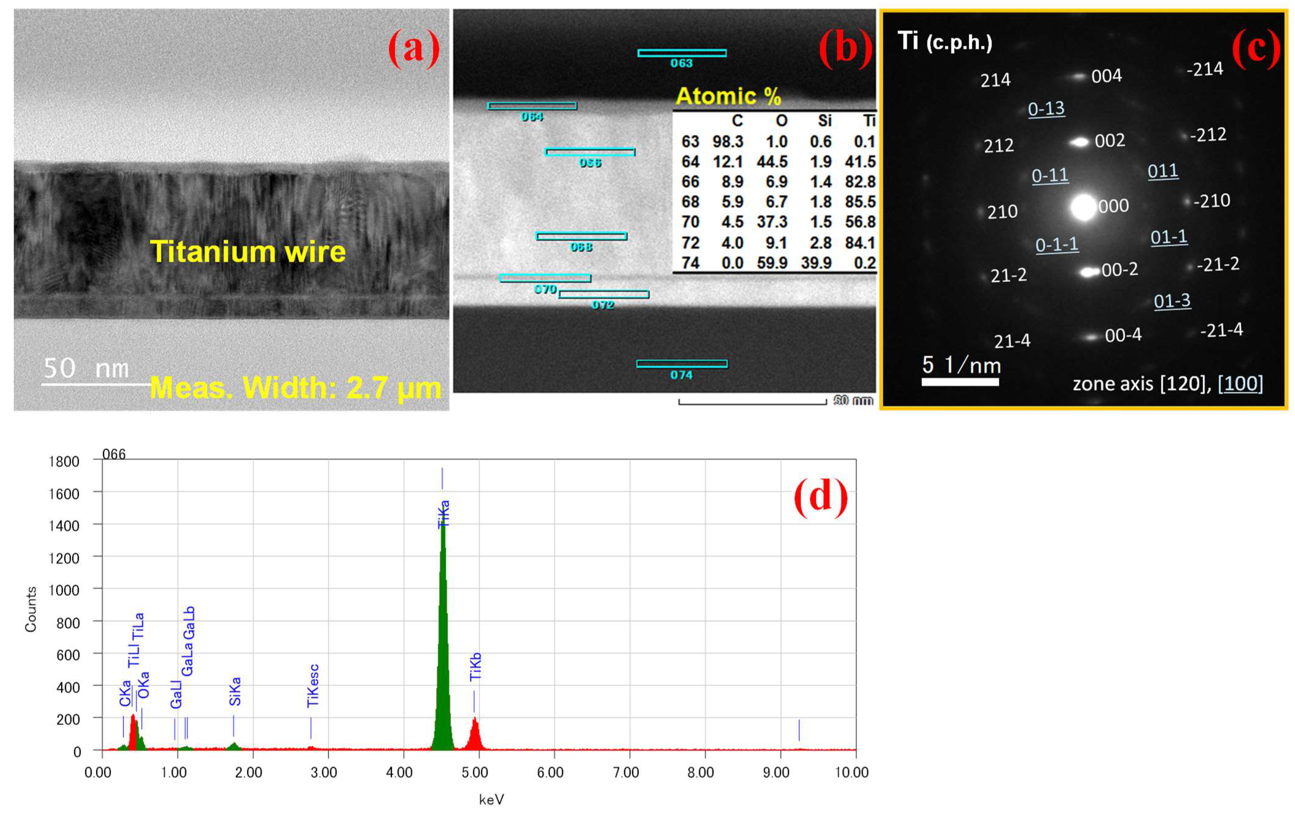
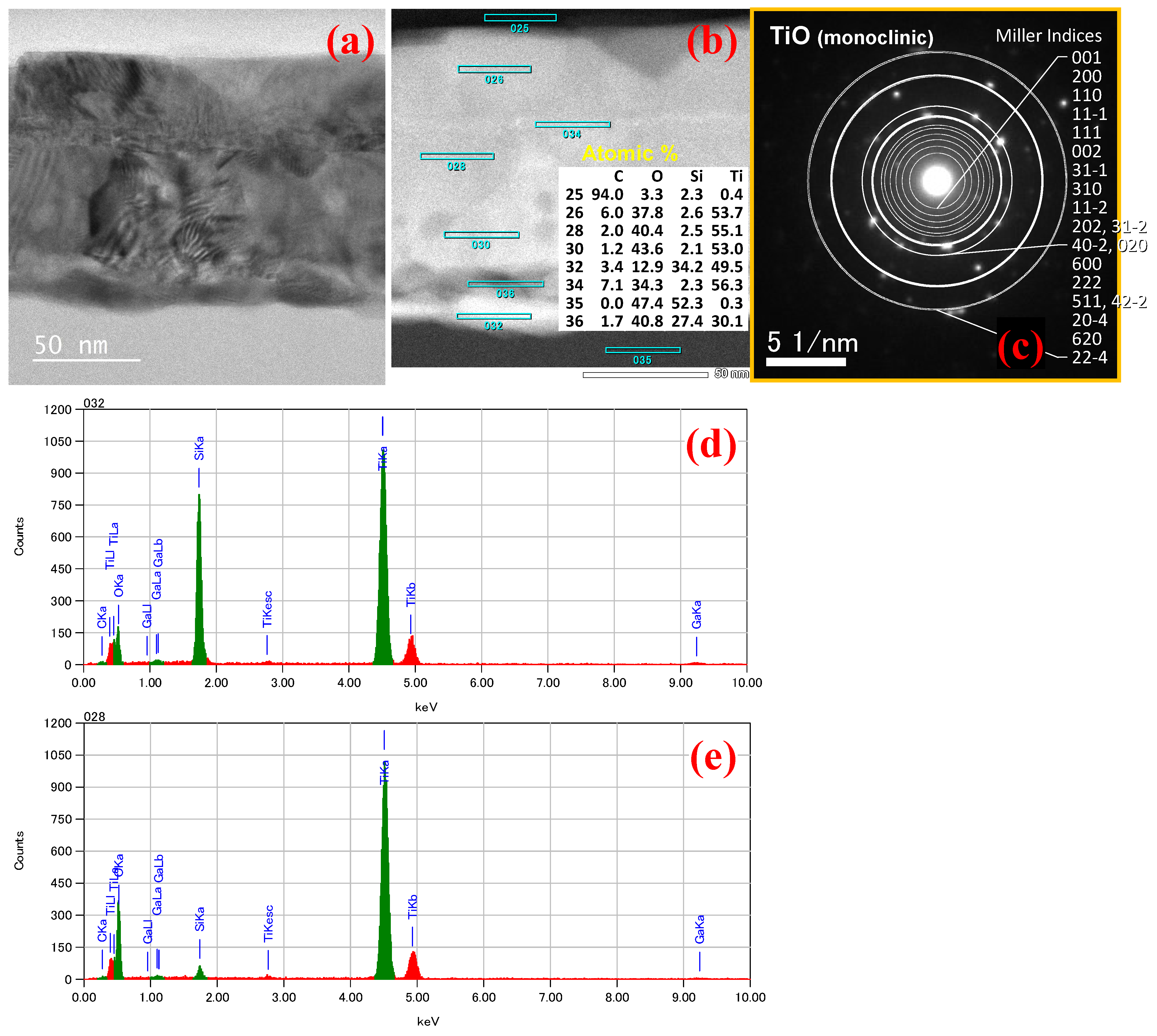
3.2. TEM Analysis on Ti Thermistors before and after Joule Heating
4. Conclusions
Author Contributions
Funding
Data Availability Statement
Acknowledgments
Conflicts of Interest
References
- Gary, S.M.; Sze, S.M. Fundamentals of Semiconductor Fabrication; John Wiley and Sons: New York, NY, USA, 2003; ISBN 9780471452386. [Google Scholar]
- Ziental, D.; Czarczynska-Goslinska, B.; Mlynarczyk, D.T.; Glowacka-Sobotta, A.; Stanisz, B.; Goslinski, T.; Sobotta, L. Nanomaterials. Nanomaterials 2020, 10, 387. [Google Scholar] [CrossRef] [PubMed]
- Yamamoto, K.; Yamaguchi, M.; Miyamaru, F.; Tani, M.; Ikeda, T.; Matsushita, A.; Koide, K.; Tatsuno, M.; Minami, Y. The Japan Society of Applied Physics Noninvasive Inspection of C-4 Explosive in Mails by Terahertz Time-Domain Spectroscopy. Jpn. J. Appl. Phys. 2004, 43, L414. [Google Scholar] [CrossRef]
- Kawase, K.; Ogawa, Y.; Watanabe, Y.; Inoue, H. Non-Destructive Terahertz Imaging of Illicit Drugs Using Spectral Fingerprints; OPTICA: Las Vegas, NV, USA, 2003; Volume 11, pp. 2549–2554. [Google Scholar] [CrossRef]
- Federici, J.F.; Schulkin, B.; Huang, F.; Gary, D.; Barat, R.; Oliveira, F.; Zimdars, D. Semiconductor Science and Technology THz imaging and sensing for security applications—explosives, weapons and drugs. Semicond. Sci. Technol. 2005, 20, S266. [Google Scholar] [CrossRef]
- Horowitz, J.D.; Thesis, M.S.; Chester, F. Carlson Center for Imaging Science, Rochester Inst. of Tech. 2017. Available online: http://www.iupac.org/dhtml_home.html (accessed on 10 December 2023).
- Woolard, D.L.; Brown, E.R.; Pepper, M.; Kemp, M. Terahertz Frequency Sensing and Imaging: A Time of Reckoning Future Applications? IEEE: Piscataway, NJ, USA, 2005; pp. 1722–1743. [Google Scholar] [CrossRef]
- Jha, K.R.; Singh, G.; Technol, I.P. Terahertz planar antennas for future wireless communication: A technical review. Infrared Phys. Technol. 2013, 60, 71–80. [Google Scholar] [CrossRef]
- Woodward, R.M.; Cole, B.E.; Wallace, V.P.; Pye, R.J.; Arnone, D.D.; Linfield, E.H.; Pepper, M.; Biol, P.M. Terahertz pulse imaging in reflection geometry of human skin cancer and skin tissue. Phys. Med. Biol. 2002, 47, 3853. [Google Scholar] [CrossRef] [PubMed]
- Nagel, M.; Bolivar, P.H.; Brucherseifer, M.; Kurz, H.; Bosserhoff, A.; Buttner, R. Integrated THz technology for label-free genetic diagnostics. Appl. Phys. Lett. 2002, 80, 154–156. [Google Scholar] [CrossRef]
- Karpowicz, N.; Zhong, H.; Zhang, C.; Lin, K.I.; Hwang, J.S.; Xu, J.; Zhang, X.C. Compact continuous-wave subterahertz system for inspection applications. Appl. Phys. Lett. 2005, 86, 054105. [Google Scholar] [CrossRef]
- Yamashita, M.; Otani, C.; Matsumoto, T.; Midoh, Y.; Miura, K.; Nakamae, K.; Nikawa, K.; Kim, S.; Murakami, H.; Tonouchi, M. THz emission characteristics from p/n junctions with metal lines under non-bias conditions for LSI failure analysis. Opt. Express 2011, 19, 10864–10873. [Google Scholar] [CrossRef]
- Kan, W.-C.; Lee, W.-S.; Cheung, W.-H.; Wallace, V.P.; Pickwell-MacPherson, E. Terahertz pulsed imaging of knee cartilage. Biomed. Opt. Express 2010, 1, 967–974. [Google Scholar] [CrossRef]
- Taylor, Z.D.; Singh, R.S.; Culjat, M.O.; Suen, J.Y.; Grundfest, W.S.; Lee, H.; Brown, E.R. Reflective terahertz imaging of porcine skin burns. Opt. Lett. 2008, 33, 1258–1260. [Google Scholar] [CrossRef]
- Schirmer, M.; Fujio, M.; Minami, M.; Miura, J.; Araki, T.; Yasui, T. Biomedical applications of a real-time terahertz color scanner. Biomed. Opt. Express 2010, 1, 354–366. [Google Scholar] [CrossRef] [PubMed]
- Nemirovsky, Y.; Svetlitza, A.; Brouk, I.; Stolyarova, S. Nanometric CMOS-SOI-NEMS Transistor for Uncooled THz Sensing. IEEE Trans. Electron Devices 2013, 60, 1575–1583. [Google Scholar] [CrossRef]
- Garn, L.E. Fundamental noise limits of thermal detectors. J. Appl. Phys. 1984, 55, 1243–1253. [Google Scholar] [CrossRef]
- Kruse, P.W. Uncooled Thermal Imaging Arrays, Systems, and Applications; SPIE: Bellingham, WA, USA, 2001; ISBN 0-8194-4122-8. [Google Scholar]
- Hay, K.A. Large format VOx microbolometer UFPA development at ITC. In Infrared Detectors and Focal Plane Arrays VIII; SPIE: Bellingham, WA, USA, 2006; Volume 6295, pp. 26–31. [Google Scholar] [CrossRef]
- Neikirk, D.P.; Lam, W.W.; Rutledge, D.B. Far-infrared microbolometer detectors. Int. J. Infrared Millim. Waves 1984, 5, 245–278. [Google Scholar] [CrossRef]
- Shimizu, T.; Moritsu, H.; Yasuoka, Y.; Gamo, K. Fabrication of Antenna-Coupled Microbolometers. Jpn. J. Appl. Phys. 1995, 34, 6352. [Google Scholar] [CrossRef]
- Son, L.N.; Tachiki, T.; Uchida, T. Fabrication and Evaluation of Thin-Film Spiral-Antenna-Coupled VOx Microbolometer by Metal–Organic Decomposition. Jpn. J. Appl. Phys. 2013, 52, 046601. [Google Scholar] [CrossRef]
- Uchida, T.; Matsushita, A.; Tachiki, T. High DC sensitivity of VOxbolometer thin films on Si3N4/SiO2membranes fabricated by metal–organic decomposition. Jpn. J. Appl. Phys. 2014, 53, 068009. [Google Scholar] [CrossRef]
- Banerjee, A.; Satoh, H.; Tiwari, A.; Apriono, C.; Rahardjo, E.T.; Hiromoto, N.; Inokawa, H. Width dependence of platinum and titanium thermistor characteristics for application in room-temperature antenna-coupled terahertz microbolometer. Jpn. J. Appl. Phys. 2017, 56, 04CC07. [Google Scholar] [CrossRef]
- Banerjee, A.; Satoh, H.; Sharma, Y.; Hiromoto, N.; Inokawa, H. Characterization of platinum and titanium thermistors for terahertz antenna-coupled bolometer applications. Sens. Actuators A Phys. 2018, 273, 49–57. [Google Scholar] [CrossRef]
- Banerjee, A.; Satoh, H.; Elamaran, D.; Sharma, Y.; Hiromoto, N.; Inokawa, H. Optimization of narrow width effect on titanium thermistor in uncooled antenna-coupled terahertz microbolometer. Jpn. J. Appl. Phys. 2018, 57, 04FC09. [Google Scholar] [CrossRef]
- Banerjee, A.; Satoh, H.; Elamaran, D.; Sharma, Y.; Hiromoto, N.; Inokawa, H. Performance improvement of on-chip integrable terahertz microbolometer arrays using nanoscale meander titanium thermistor. J. Appl. Phys. 2019, 125, 214502. [Google Scholar] [CrossRef]
- Peter, H.B.; Nagel, M.; Richter, F.; Brucherseifer, M.; Kurz, H.; Bosserhoff, A.; Büttner, R. Label–free THz sensing of genetic sequences: Towards ‘THz biochips’. Philos. Trans. R. Soc. A Math. Phys. Eng. Sci. 2003, 362, 323–335. [Google Scholar] [CrossRef]
- Ferguson, B.; Zhang, X.C. Materials for terahertz science and technology. Nature Mater. 2002, 1, 26–33. [Google Scholar] [CrossRef]
- Tonouchi, M. Cutting-edge terahertz technology. Nat. Photon. 2007, 1, 97–105. [Google Scholar] [CrossRef]
- Williams, B.S. Terahertz quantum-cascade lasers. Nat. Photon. 2007, 1, 517–525. [Google Scholar] [CrossRef]
- Watts, C.M.; Shrekenhamer, D.; Montoya, J.; Lipworth, G.; Hunt, J.; Sleasman, T.; Krishna, S.; Smith, D.R.; Padilla, W.J. Terahertz compressive imaging with metamaterial spatial light modulators. Nat. Photon. 2014, 8, 605–609. [Google Scholar] [CrossRef]
- Han, D.P.; Fujiki, R.; Takahashi, R.; Ueshima, Y.; Ueda, S.; Lu, W.; Iwaya, M.; Takeuchi, T.; Kamiyama, S.; Akasaki, I. n-type GaN surface etched green light-emitting diode to reduce non-radiative recombination centers. Appl. Phys. Lett. 2021, 118, 021102. [Google Scholar] [CrossRef]
- But, D.B.; Drexler, C.; Sakhno, M.V.; Dyakonova, N.; Drachenko, O.; Sizov, F.F.; Gutin, A.; Ganichev, S.D.; Knap, W. Nonlinear photoresponse of field effect transistors terahertz detectors at high irradiation intensities. J. Appl. Phys. 2014, 115, 164514. [Google Scholar] [CrossRef]
- Yang, X.; Vorobiev, A.; Generalov, A.; Andersson, M.A.; Stake, J. A flexible graphene terahertz detector. Appl. Phys. Lett. 2017, 11, 1021102. [Google Scholar] [CrossRef]
- Huang, X.; Leng, T.; Zhu, M.; Zhang, X.; Chen, J.C.; Chang, K.H.; Aqeeli, M.; Geim, A.K.; Novoselov, K.S.; Hu, Z. Highly Flexible and Conductive Printed Graphene for Wireless Wearable Communications Applications. Sci. Rep. 2015, 5, 18298. [Google Scholar] [CrossRef]
- Tiwari, A.; Satoh, H.; Aoki, M.; Takeda, M.; Hiromoto, N.; Inokawa, H. Fabrication and analytical modeling of integrated heater and thermistor for antenna-coupled bolometers. Sens. Actuators A Phys. 2015, 222, 160–166. [Google Scholar] [CrossRef]
- Elamaran, D.; Suzuki, Y.; Satoh, H.; Banerjee, A.; Hiromoto, N.; Inokawa, H. Performance Comparison of SOI-Based Temperature Sensors for Room-Temperature Terahertz Antenna-Coupled Bolometers: MOSFET, PN Junction Diode and Resistor. Micromachines 2020, 11, 718. [Google Scholar] [CrossRef] [PubMed]
- Banerjee, A.; Vajandar, S.; Basu, T. Prospects in Medical Applications of Terahertz Waves. In Terahertz Biomedical and Healthcare Technologies; Elsevier: Amsterdam, The Netherlands, 2020; pp. 225–239. [Google Scholar] [CrossRef]
- Samanta, D.; Karthikeyan, M.; Banerjee, A.; Inokawa, H. Tunable graphene nanopatch antenna design for on-chip integrated terahertz detector arrays with potential application in cancer imaging. Nanomedicine 2021, 16, 1035–1047. [Google Scholar] [CrossRef] [PubMed]
- Kašalynas, I.; Venckevičius, R.; Minkevičius, L.; Sešek, A.; Wahaia, F.; Tamošiūnas, V.; Voisiat, B.; Seliuta, D.; Valušis, G.; Švigelj, A.; et al. Spectroscopic Terahertz Imaging at Room Temperature Employing Microbolometer Terahertz Sensors and Its Application to the Study of Carcinoma Tissues. Sensors 2016, 16, 432. [Google Scholar] [CrossRef]
- Fukasawa, R. Terahertz Imaging: Widespread Industrial Application in Non-destructive Inspection and Chemical Analysis. In IEEE Transactions on Terahertz Science and Technology; IEEE: Piscataway, NJ, USA, 2015; Available online: https://ieeexplore.ieee.org/document/7335441 (accessed on 10 December 2023).
- Kim, R.H.J.; Liu, Z.; Huang, C.; Park, J.M.; Haeuser, S.J.; Song, Z.; Yan, Y.; Yao, Y.; Luo, L.; Wang, J. Terahertz Nanoimaging of Perovskite Solar Cell Materials. ACS Photon. 2022, 9, 3550–3556. [Google Scholar] [CrossRef]
- Hempel, H.; Savenjie, T.J.; Stolterfoht, M.; Neu, J.; Failla, M.; Paingad, V.C.; Kužel, P.; Heilweil, E.J.; Spies, J.A.; Schleuning, M.; et al. Predicting Solar Cell Performance from Terahertz and Microwave Spectroscopy. Adv. Energy Mater. 2022, 12, 2102776. [Google Scholar] [CrossRef]
- Nakanishi, H.; Ito, A.; Takayama, K.; Kawayama, I.; Murakami, H.; Tonouchi, M. Comparison between laser terahertz emission microscope and conventional methods for analysis of polycrystalline silicon solar cell. AIP Adv. 2015, 5, 117129. [Google Scholar] [CrossRef]
- Yang, H.U.; Raschke, M.B. Resonant optical gradient force interaction for nano-imaging and -spectroscopy. New J. Phys. 2016, 18, 053042. [Google Scholar] [CrossRef]
- Murakami, H.; Serita, K.; Maekawa, Y.; Fujiwara, S.; Matsuda, E.; Kim, S.; Kawayama, I.; Tonouchi, M. Scanning laser THz imaging system. J. Phys. D Appl. Phys. 2014, 47, 374007. [Google Scholar] [CrossRef]
- Khan, S.; Acharyya, A.; Inokawa, H.; Satoh, H.; Biswas, A.; Dhar, R.S.; Banerjee, A.; Seteikin, A.Y. Terahertz Radiation from High Electron Mobility Avalanche Transit Time Sources Prospective for Biomedical Spectroscopy. Photonics 2023, 10, 800. [Google Scholar] [CrossRef]
- Carranza, I.E. Metamaterial Based CMOS Terahertz Focal Plane Array. Ph.D. Thesis, University of Glasgow, London, UK, 2015. Available online: http://theses.gla.ac.uk/id/eprint/6955 (accessed on 10 December 2023).
- Cheng, Y.L.; Wei, B.J.; Shih, F.H.; Wang, Y.L. Stability and Reliability of Ti/TiN as a Thin Film Resistor. ECS J. Solid State Sci. Technol. 2012, 2, Q12–Q15. [Google Scholar] [CrossRef]
- Tanaka, A.; Matsumoto, S.; Tsukamoto, N.; Itoh, S.; Chiba, K.; Endoh, T.; Nakazato, A.; Okuyama, K.; Kumazawa, Y.; Hijikawa, M.; et al. Infrared focal plane array incorporating silicon IC process compatible bolometer. IEEE Trans. Electron Devices 1996, 43, 1844–1850. [Google Scholar] [CrossRef]
- Zhang, S.; Yang, Y.; Sadeghipour, S.M.; Asheghi, M. Thermal Characterization of the 144 nm GMR Layer Using Microfabricated Suspended Structures. In Proceedings of the ASME 2003 Heat Transfer Summer Conference, Las Vegas, NV, USA, 21–23 July 2003; pp. 89–92. [Google Scholar] [CrossRef]
- Liu, W.; Asheghi, M. Thermal conduction in ultrathin pure and doped single-crystal silicon layers at high temperatures. J. Appl. Phys. 2005, 98, 123523. [Google Scholar] [CrossRef]
- Watanabé, D.; Castles, J.R.; Jostsons, A.; Malin, A.S. The ordered structure of TiO. Acta Crystallogr. 1967, 23, 307–313. [Google Scholar] [CrossRef]


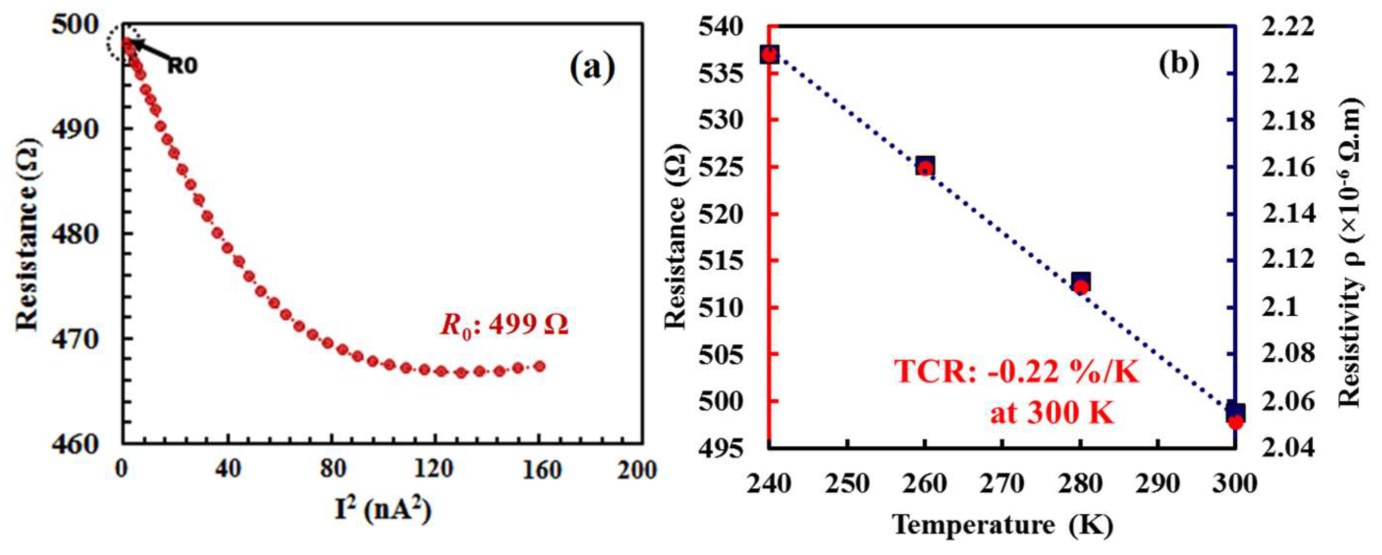
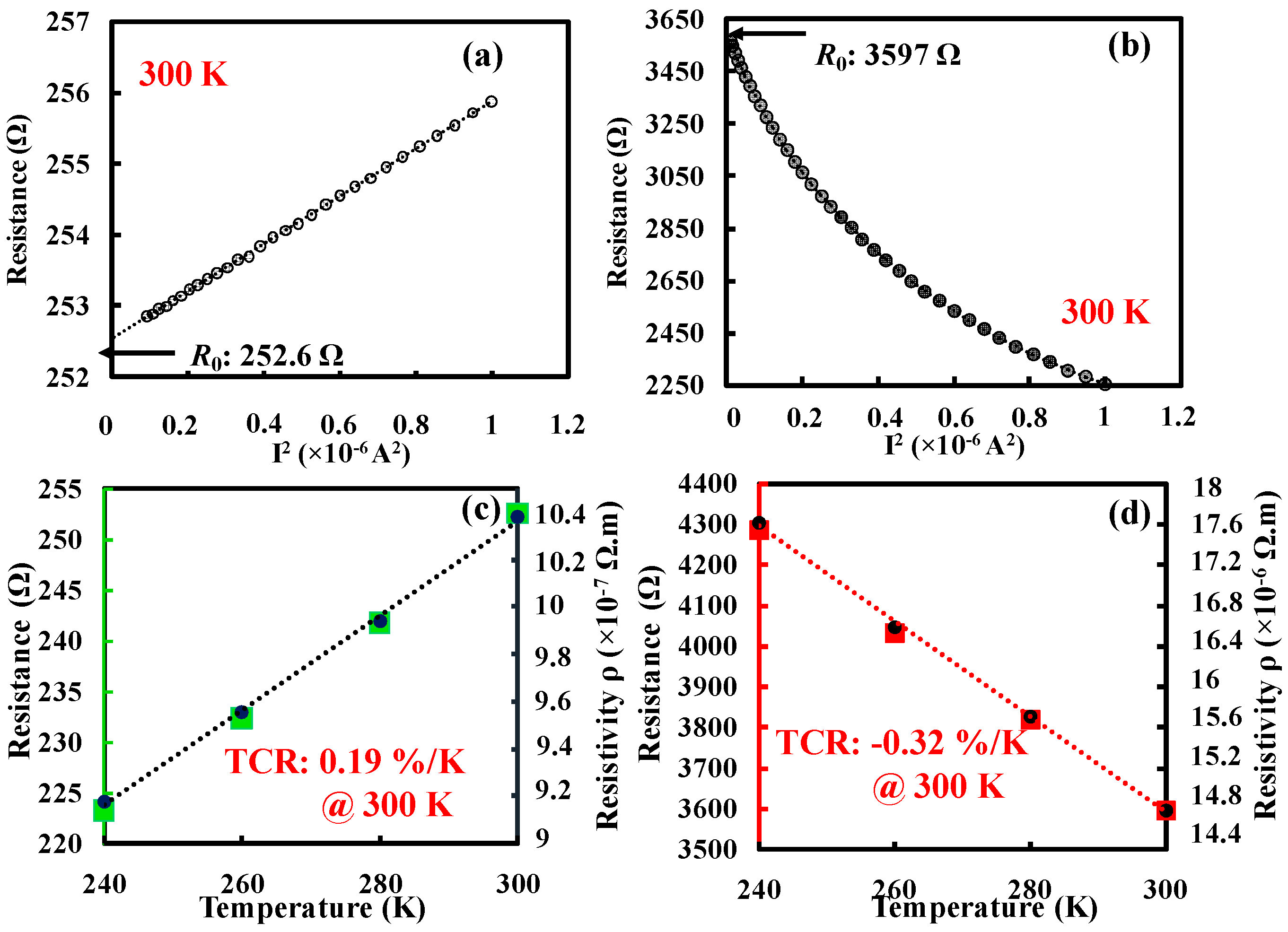
| Device Name | Resistance (Ω) | TCR (%/K) | dR/dI2/R02 (1/W) | |||
|---|---|---|---|---|---|---|
| Before Annealing | After Annealing | Before Annealing | After Annealing | Before Annealing | After Annealing | |
| UR | 253 | 3597 | 0.19 | −0.31 | 52.2 | −249 |
| UL | 254 | 3140 | 0.19 | −0.33 | 52.9 | −178 |
| LR | 250 | 4224 | 0.19 | −0.5 | 47.8 | −864 |
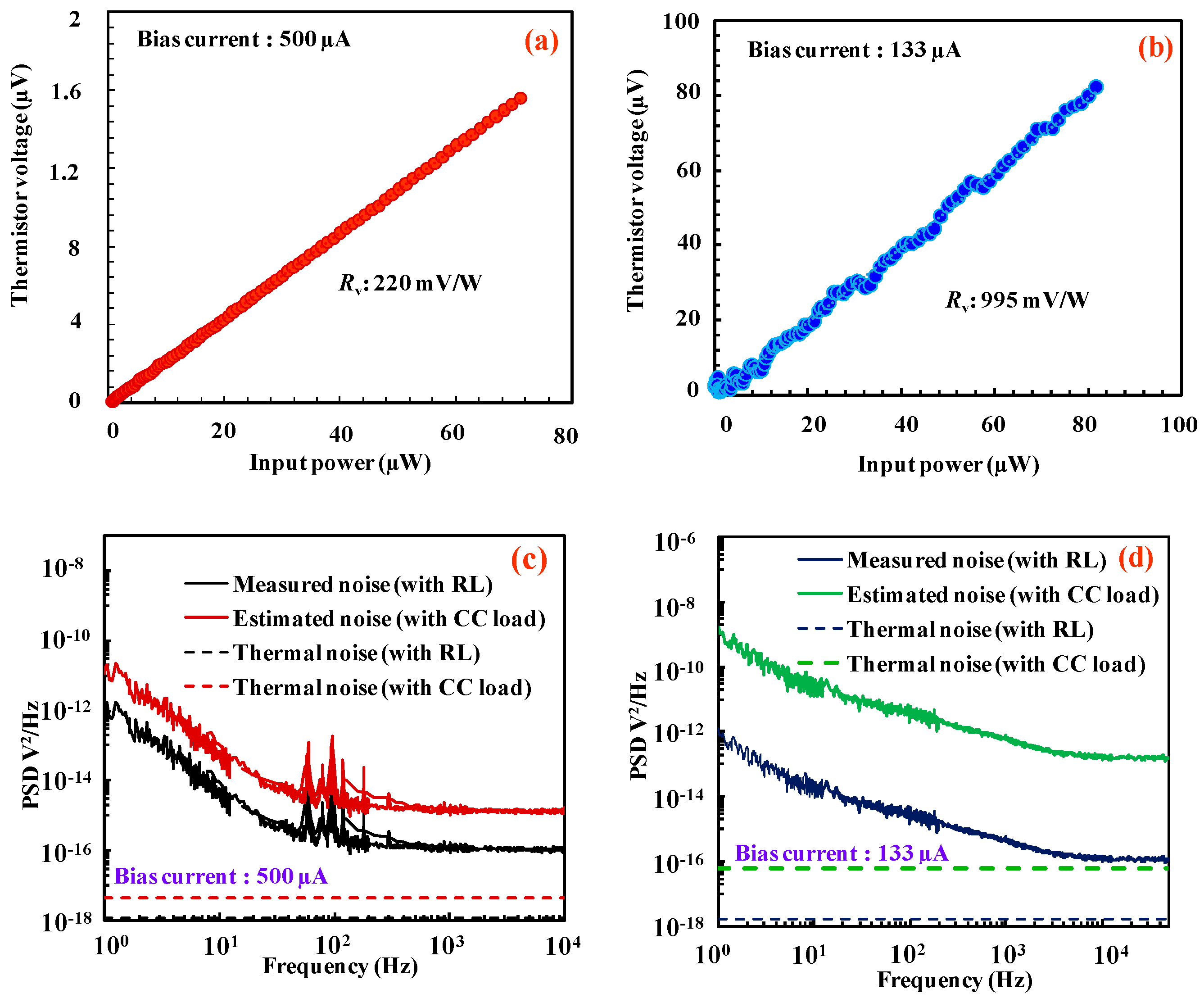
| Parameter | Factor | Remarks |
|---|---|---|
| Electrical resistance (Re) * | K | After Joule heating |
| Thermal resistance (Rt) * | K | Rt ∝ Re |
| Bias voltage (Vb) | 1 | |
| Bias current (Ib), input power (Pin) due to bias | 1/K | Pin = Ib2 × Re |
| Temperature rise (ΔT) due to bias | 1 | ΔT ∝ Pin × Rt |
| Temperature rise by optical input (ΔTopt) | K | ΔT ∝ Popt × Rt (Popt: const.) |
| Output voltage (Vout) | K | Vout ∝ Ib × Re × ΔTopt |
| Responsivity (Rv) | K | Rv ∝ Vout/Popt |
Disclaimer/Publisher’s Note: The statements, opinions and data contained in all publications are solely those of the individual author(s) and contributor(s) and not of MDPI and/or the editor(s). MDPI and/or the editor(s) disclaim responsibility for any injury to people or property resulting from any ideas, methods, instructions or products referred to in the content. |
© 2024 by the authors. Licensee MDPI, Basel, Switzerland. This article is an open access article distributed under the terms and conditions of the Creative Commons Attribution (CC BY) license (https://creativecommons.org/licenses/by/4.0/).
Share and Cite
Elamaran, D.; Akiba, K.; Satoh, H.; Banerjee, A.; Hiromoto, N.; Inokawa, H. On-Chip Modification of Titanium Electrothermal Characteristics by Joule Heating: Application to Terahertz Microbolometer. Nanomaterials 2024, 14, 225. https://doi.org/10.3390/nano14020225
Elamaran D, Akiba K, Satoh H, Banerjee A, Hiromoto N, Inokawa H. On-Chip Modification of Titanium Electrothermal Characteristics by Joule Heating: Application to Terahertz Microbolometer. Nanomaterials. 2024; 14(2):225. https://doi.org/10.3390/nano14020225
Chicago/Turabian StyleElamaran, Durgadevi, Ko Akiba, Hiroaki Satoh, Amit Banerjee, Norihisa Hiromoto, and Hiroshi Inokawa. 2024. "On-Chip Modification of Titanium Electrothermal Characteristics by Joule Heating: Application to Terahertz Microbolometer" Nanomaterials 14, no. 2: 225. https://doi.org/10.3390/nano14020225