
Coexistent VO2 (M) and VO2 (B) Polymorphous Thin Films with Multiphase-Driven Insulator–Metal Transition
by
Mengxia Qiu
1,2,
Wanli Yang
3,
Peiran Xu
1,
Tiantian Huang
1,
Xin Chen
1,3,* and
Ning Dai
1,2,3,* 1
State Key Laboratory of Infrared Physics, Shanghai Institute of Technical Physics, Chinese Academy of Sciences, Shanghai 200083, China
2
School of Physical Science and Technology, ShanghaiTech University, Shanghai 201210, China
3
Hangzhou Institute for Advanced Study, University of Chinese Academy of Sciences, Hangzhou 310024, China
*
Authors to whom correspondence should be addressed.
Nanomaterials 2023, 13(9), 1514; https://doi.org/10.3390/nano13091514
Submission received: 11 April 2023
/
Revised: 25 April 2023
/
Accepted: 27 April 2023
/
Published: 28 April 2023
(This article belongs to the Special Issue Research on Nano-Lattice)
Abstract
:Reversible insulator–metal transition (IMT) and structure phase change in vanadium dioxide (VO2) remain vital and challenging with complex polymorphs. It is always essential to understand the polymorphs that coexist in desired VO2 materials and their IMT behaviors. Different electrical properties and lattice alignments in VO2 (M) and VO2 (B) phases have enabled the creation of versatile functional devices. Here, we present polymorphous VO2 thin films with coexistent VO2 (M) and VO2 (B) phases and phase-dependent IMT behaviors. The presence of VO2 (B) phases may induce lattice distortions in VO2 (M). The plane spacing of (011)M in the VO2 (M) phase becomes widened, and the V-V and V-O vibrations shift when more VO2 (B) phase exists in the VO2 (M) matrix. Significantly, the coexisting VO2 (B) phases promote the IMT temperature of the polymorphous VO2 thin films. We expect that such coexistent polymorphs and IMT variations would help us to understand the microstructures and IMT in the desired VO2 materials and contribute to advanced electronic transistors and optoelectronic devices.
1. Introduction
Polarizable metal–oxygen bonds [1] and strong correlations among localized valance electrons in transition metal oxides [2,3] have sparked intensive interest, and they have shown promise in optoelectronics [4,5,6,7], sensors [8,9,10,11] and catalysis [12,13,14,15]. As one of the correlated electronic oxides, VO2 has several polymorphs, including VO2 (R) [16], VO2 (B) [17] and VO2 (M) [18]. Various crystalline symmetries and electronic structures in these polymorphs have shown versatile potential applications [19,20,21]. Wherein, the stable monoclinic VO2 (M) (P21/c) phase has attracted widespread attention due to a reversible IMT near 340 K. Lattice variations are often connected with the transformation between delocalized and localized states during IMT in VO2. Meanwhile, pure electronic behaviors have been observed due to strain-engineering and lattice-freezing during IMT processes [22,23]. Companied with IMT, structural distortion generally occurs within a first-order phase change from a low-temperature monoclinic VO2 (M) phase to a high-temperature rutile VO2 (R) phase [24]. In the insulating VO2 (M) phase, adjacent vanadium atoms form zigzag chains with two types of vanadium–vanadium bond lengths along the cR axis, and the shorter one may form a vanadium–vanadium dimer, which makes the electrons localized [25].
The polymorphous lattices and crystalline phases often affect electrical and optical behaviors in VO2, which are closely related to the vanadium–vanadium bonds. Different from the VO2 (M) phase, the VO2 (B) (C2/m) phase is a Wadsley phase with a quasi-layered monoclinic structure [26] and undergoes IMT over a wide temperature range from 180 K to 300 K [27], while the vanadium–vanadium pairs induce layered alignments. It is noted that the edge-sharing VO6 octahedra in the VO2(B) phase aid ion diffusion and gas reduction in ion batteries and energy storage devices [28]. When VO2 (B)-like vanadium–vanadium bonds exist in VO2 (M) lattices, the microstructures, the electronic states and IMT behaviors in VO2 (M) may be modified due to the variations in crystal field energy and orbital occupancies near the Fermi level [29]. Actually, it is still of significance and challenging to understand microstructural changes and IMT in the coexistent polymorphs in VO2 towards versatile applications [30].
Herein, we described the lattice variations and IMT behaviors in VO2 thin films with coexistent VO2 (M) and VO2 (B) phases. The widened plane spacing of (011)M and varied V-V and V-O phonon vibrations were induced by the coexisting VO2 (B) phase in the VO2 (M) thin films, as confirmed via Raman spectra and X-ray diffraction (XRD). The IMT temperature for the VO2 (M) thin films increased when more VO2 (B) phases were presented in the polymorphous thin films. We expected such phase-dependent IMT behaviors to aid our understanding of polymorphous lattice variations and electronic phase changes in correlated vanadium oxides and enable the fabrication of advanced optical, electronic and even energy devices.
2. Results and Discussion
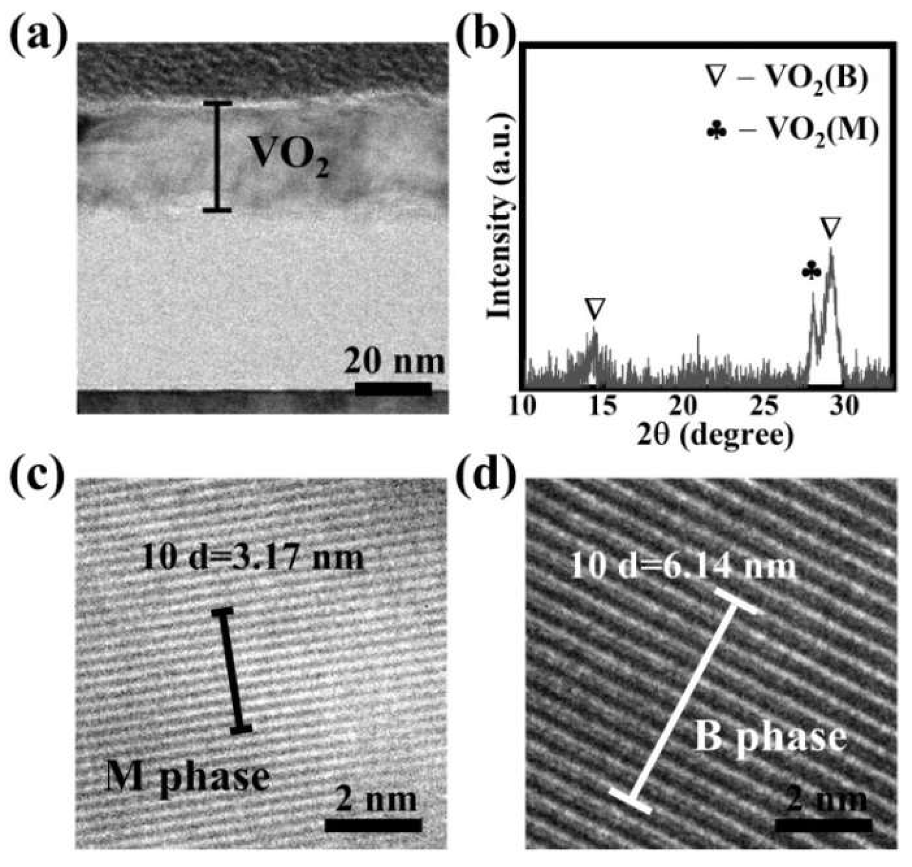
According to previous work [31], we exploited atomic layer deposition and post-annealing processes to obtain coexistent VO2 (M) and VO2 (B) phases in the VO2 thin films. Figure 1a displays a cross-sectional TEM image for a ~32 nm thick VO2 thin film. When the XRD measurement was performed on the VO2 thin film, diffraction peaks were obvious in the XRD patterns, as shown in Figure 1b. The diffraction peaks near 2θ = 28.00° were ascribed to monoclinic VO2(PDF #09-0142) [29], indicating the presence of a VO2 (M) phase in the resulting thin film. In the TEM image (Figure 1c), obvious lattice fringes were also found with a d-spacing of 10d ≈ 3.17 nm, which further confirmed the existence of a VO2 (M) phase [32]. As expected for the VO2 (M) phase, the VO2 (B) phase was also found in the resulting VO2 thin film, as shown in Figure 1. XRD peaks near 2θ = 14.40° and 2θ = 29.00° in Figure 1b corresponded to VO2 (B) (PDF #81-2392) [33], which was also verified by a d-spacing of 10d ≈ 6.14 nm for the lattice fringes in VO2 (B) [34] in Figure 1d. All these results suggested the presence of coexistent VO2 (M) and VO2 (B) phases in the as-prepared VO2 thin film.
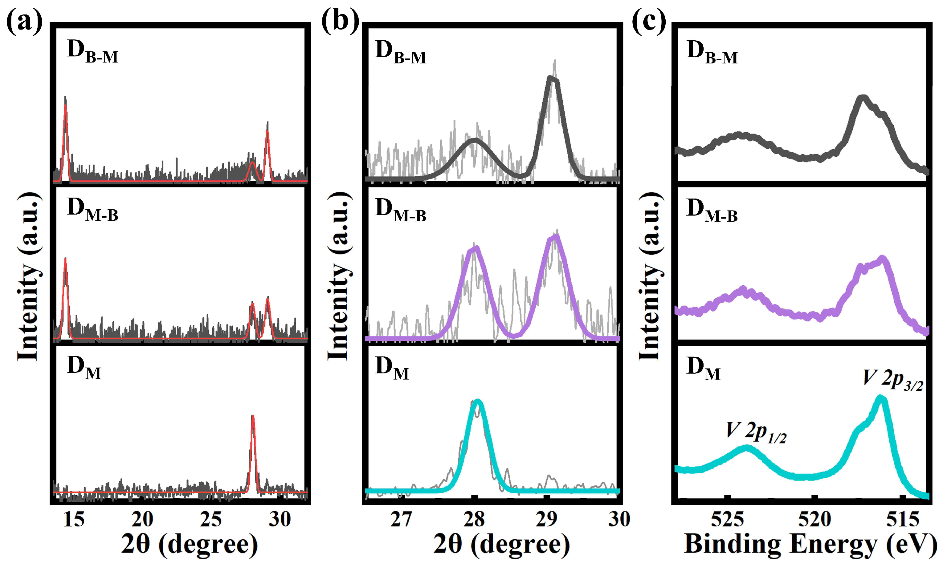
As mentioned above, the microstructures of VO2 (M) thin films may be changed due to the existence of the VO2 (B) phase. Figure 2 displays the microstructure variations in VO2 (M) thin films when the content of VO2 (B) phases increased in the as-prepared polymorphous VO2 thin films. Figure 2a,b displays the XRD patterns of the polymorphous VO2 thin films with various VO2 (B) contents, referred to as DM (VO2 thin film with few VO2 (B) phases), DM-B (VO2 thin film with some VO2 (B) phases) and DB-M (VO2 thin film with more VO2 (B) phases). The XRD peaks around 2θ = 28.00° appeared in all DM, DM-B and DB-M thin films and were assigned to the (011) plane of VO2 (M). Notably, XRD peaks near 2θ = 14.40° and 2θ = 29.00° were obvious and found in the DM-B and DB-M thin films, and they were assigned to the (001) and (002) planes in VO2 (B) (PDF #81-2392), respectively. For the DM thin film, XRD peaks near 2θ = 14.40 ° were hardly observed, which indicated the main lattice was the VO2 (M) phase in the DM thin film, and few VO2 (B) phases might have existed. We also found the intensity ratios at the XRD peaks near 2θ = 28.00° and 2θ = 29.00° were different in the case of the DM-B and DB-M thin films. For the DB-M thin film, a larger ratio implied that there was more VO2 (B) phases in the VO2 thin films with coexistent VO2 (M) and VO2 (B) phases. Figure 2a suggests that the XRD patterns were different and related to the content of VO2 (B) phases. More VO2 (B) phases would have enhanced the intensity at about 2θ = 29.00°, while the intensity declined at about 2θ = 28.00° for VO2 (M). The color changed in the temperature-dependent optical images for the DM-B thin film upon heating (Figure S1 in SI), which indicated that the VO2 (M) phase was dominant in the DM-B thin film. In contrast, the invariant color in the optical images (Figure S1 in SI) above room temperature for the DB-M thin film implied that the VO2 (B) phase dominated in the DB-M thin film, because the IMT process associated with the VO2 (B) phase occurred between 180 K and 300 K. All measurements and analyses above suggested that the contents of the VO2 (B) phase in the DM, DM-B and DB-M thin films increased gradually.
Subsequently, we fitted the XRD curves and checked the peak variations for the (011)M plane in the VO2 (M) phase, as shown in Figure 2b. For the DM, DM-B and DB-M thin films, the corresponding 2θ were about 28.05°, 28.00° and 27.98°, respectively. According to Bragg’s law [35], the d-spacings for the (011)M plane in VO2 (M) were calculated to be about 3.179 Å, 3.184 Å and 3.186 Å by using the above 2θ values for the DM, DM-B and DB-M thin films, respectively. The d-spacing of (011)M plane directly impacted the distance of the V-V lattice along the cR axis, which was related to electron–electron and electron–phonon interactions and the IMT behaviors of VO2 (M) [25]. The above results suggested that the VO2 (B) phases may affect the lattice, especially the d-spacing of the (011)M plane in VO2 (M) in the VO2 thin films with coexistent VO2 (M) and VO2 (B) phases. VO2 (B) usually formed in an oxygen-excess environment, while VO2 (M) formed in an oxygen-deficient environment. An appropriate amount of V could support an environment where VO2 (B) was formed [36]. The thin films with more VO2 (B) phases annealed at a slower heating rate, resulting in the formation of VO2 (B) at a lower temperature and insufficient activation energy to fully convert to stable VO2 (R), which would transform to VO2 (M) below about 340 K [37]. X-ray photoelectron spectroscopy (XPS) measurements were used to analyze the binding energy and oxidation state related to vanadium [38] (Figure 2c and Figure S2). Figure S2 indicates the fitted peaks for varied oxidation states involving V+4 (with binding energies at about 516.2 eV and 523.4 eV) and V+5 (with binding energies at about 517.4 eV and 525.2 eV) for the V 2p core-level peaks [38]. We made calculations according to the XPS peaks and found that the valence of V+4 was dominant in the DB-M (~57.5%), DM-B (~59.2%) and DM (~67.6%) thin films, while the V+5 contents in the DB-M and DM-B thin films were higher than that in the DM thin film. The presence of V+5 might have been induced by surface oxidation and adsorption or the precursor of vanadium pentoxide [38]. Noticeably, the binding energy between vanadium atoms had a tendency to decrease from the DM to DM-B, and then to DB-M thin films (Figure 2c). As verified in the XRD patterns, the XPS spectra suggested that the increased binding energy possibly corresponded to more VO2 (B) existing in the polymorphous thin films. The layered lattice alignments and surface-induced V+5 components might have increased the binding energy and stabilized the VO2 (B) phases in the DM-B and DB-M thin films [36,39].
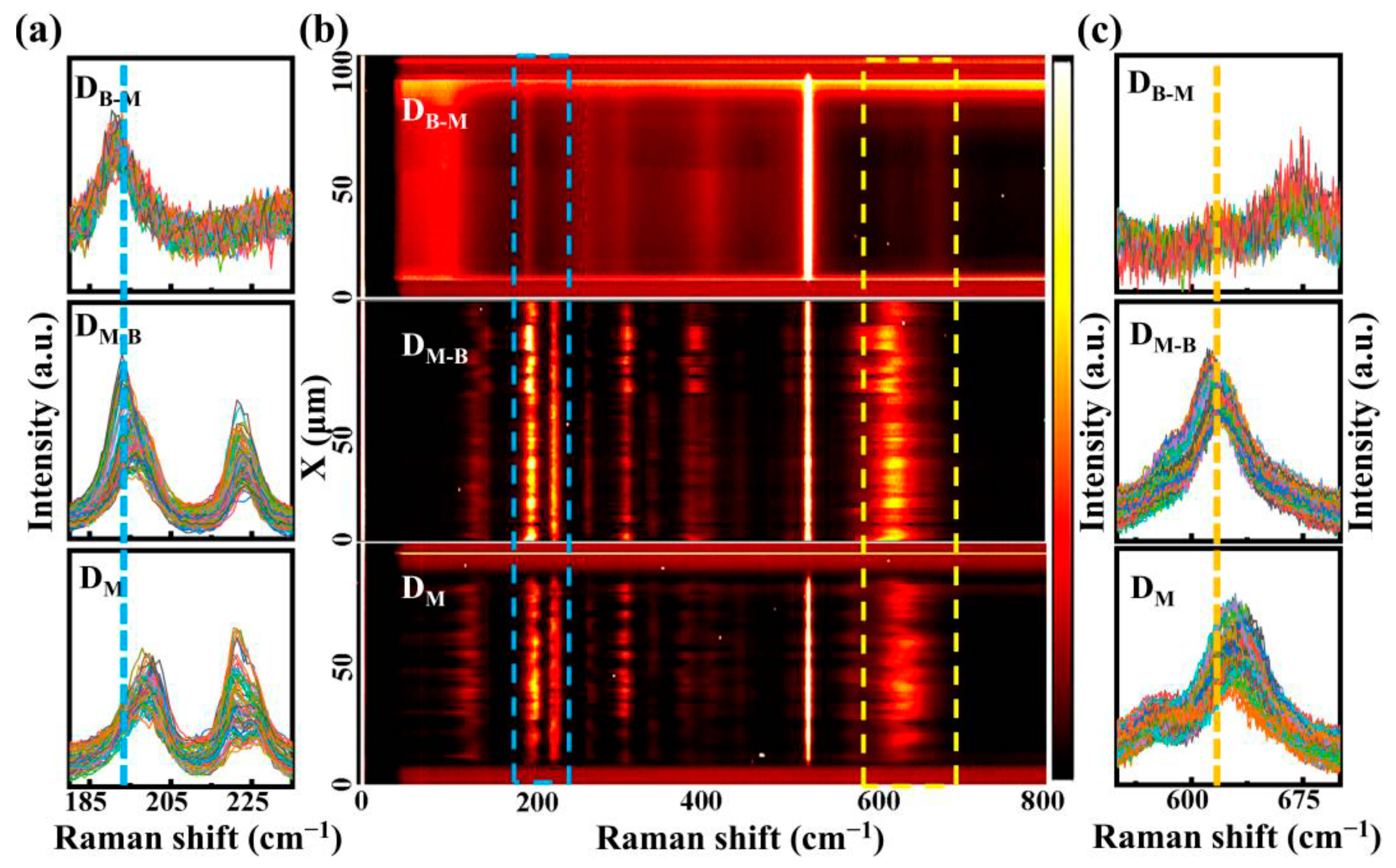
Raman spectra were adopted to identify the phases and lattice distortion in the DM, DM-B and DB-M thin films, as shown in Figure 3 and Figure S3. The distinguishable Raman shifts at about 137, 195, 224 and 615 cm−1 corresponded to the VO2 (M) in the DM and DM-B thin films [40], while the one at about 520 cm−1 was from silicon substrate. For the DB-M thin film, the Raman vibration modes at around 96, 191, 403 and 668 cm−1 were obvious and assigned to VO2 (B). The strong Raman peaks (520 cm−1) from silicon substrate indicated a deeper detective depth, which implied that the vibration modes of the whole thin film could be obtained along the vertical direction. The vibration mode at about 96 cm−1 corresponded to the translations of adjacent layers, and the vibration modes at around 191 and 403 cm−1 were related to the bending and stretching of the V-O-V structure in VO2 (B) [40]. Generally, the Raman shift at about 195 cm−1 (referred as ωV1) corresponded to the tilting motion of the V-V dimer, while the one at around 615 cm−1 (referred as ωV-O) was used to identify the V-O bond vibrations in VO2 [41]. Line-scanned Raman mapping in Figure 3 further displays the variations in the phonon vibration modes in the DM, DM-B and DB-M thin films. Here, about 100 statistical points were obtained with a scan length of 100 µm and a step of 1 µm during micro-Raman mapping. The thermal effect of the laser could be ignored because no obvious shift was found at 520 cm−1 for the silicon substrates [42]. Figure 3a,c show the Raman details at each scan position around 194 cm−1 (dashed blue box in Figure 3b) and 640 cm−1 (dashed yellow box in Figure 3b) for the DM, DM-B and DB-M thin films. In Figure 3a, Raman peaks shift towards low frequencies from around 198.5 cm−1 in the DM, to around 195 cm−1 in the DM-B, and then to around 191 cm−1 in the DB-M thin film. The Raman peak around 224 cm−1 for the VO2 (M) phase was observed in both the DM and DM-B thin films, while this peak was hardly observed in the case of the DB-M thin film. As shown in Figure 3c, the ωV-O peak around 668 cm−1 was obvious in the DB-M thin film, while the ones around 629 cm−1 and 619 cm−1 were for the DM and DM-B thin films, respectively. The above peaks indicated the variations in the ωV1 and ωV-O modes in the DM, DM-B and DB-M thin films. When comparing the varied ωV1 and ωV-O modes in the DM to DM-B thin films, we found an obvious shift because of the presence of VO2 (B), as shown in Figure 3 and Figure S3. In the DM thin film, the ωV-O peaks were dispersed and changed with the scanning position, while the ωV-O peaks in the DM-B thin film shifted and were concentrated. Meanwhile, the VO2 (B) domains were distributed in the DM-B film, which may have induced an abrupt shift [43]. For the DM and DM-B thin films, the variations in the ωV-O modes were different, which may have been attributed to the content or grain size of the VO2 (B) phase [43,44] in the corresponding thin films. In addition, the characteristic peaks around 668 cm−1 for VO2 (B) kept in the DB-M thin film. In general, the phonon behavior in the DB-M thin film was mainly attributed to the VO2 (B) phase. All these results further verified the role of VO2 (B) in the DM, DM-B and DB-M thin films, which were consistent with those indicated during the above XRD measurements.
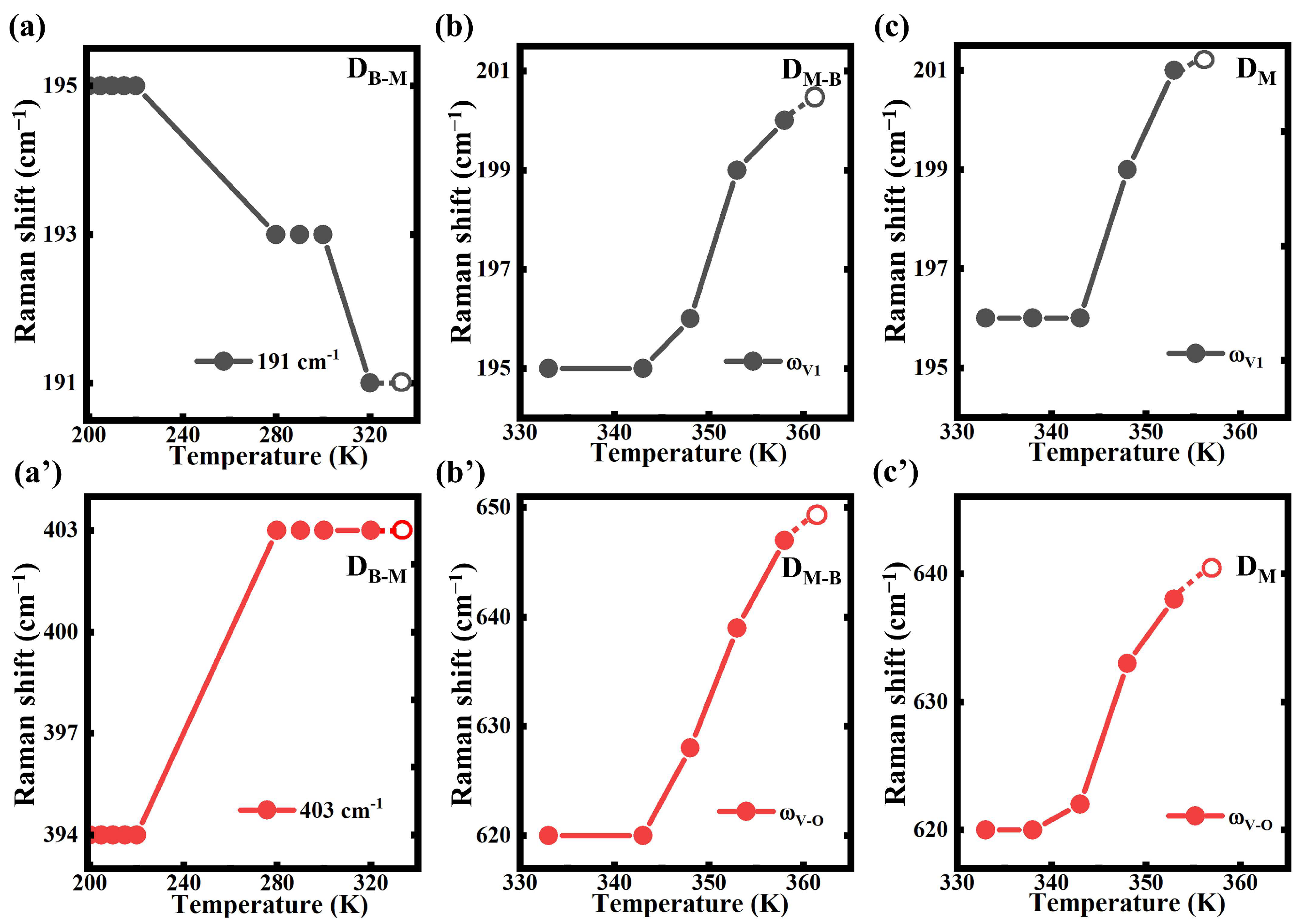
As shown in Figure 4 and Figure S4, variable-temperature Raman measurements were taken to detect the thermal-induced structural evolutions in the DB-M, DM-B and DM thin films. Figure 4a displays the peak variations in the temperature-dependent Raman spectra for the DB-M. The two modes at around ~191 and 400 cm−1 were related to the bending and stretching vibration of the V-O-V structure in the VO2 (B) phase. When the temperature rose from 220 K to 280 K, the mode at ~394 cm−1 shifted to ~403 cm−1 (Figure 4a’). The vibration mode around ~195 cm−1 at 200 K shifted to ~193 cm−1 at 280 K, and then to ~191 cm−1 at 320 K. Meanwhile, the intensity of the Raman peak around ~195 cm−1 increased obviously from 200 K to 320 K (Figure 4a). There was no significant change in Raman spectra for the DB-M above 320 K. Due to the semimetal nature of the VO2 (B) phase at room temperature [44], we could still observe a relatively resolvable Raman shift. In the DM-B thin film, the ωV1 vibration mode of ~195 cm−1 at 343 K shifted to ~201 cm−1 at 358 K, while the ωV-O vibration mode changed from ~620 cm−1 to ~647 cm−1 due to the thermal-induced lattice distortion. Above 358 K, the ωV1 and ωV-O modes vanished due to the formation of metallic rutile VO2 during IMT (Figure 4b, b’ and Figure S4b). The metallic rutile phase did not contribute to a discriminable Raman signal, and thus, a flat Raman spectrum indicated its presence. Meanwhile, in the DM thin film, the ωV1 vibrations suddenly changed from ~195 cm−1 at 343 K to ~201 cm−1 at 353 K, and the ωV-O mode at 620 cm−1 shifted to 638 cm−1. In Figure 4c,c’ and Figure S4c, both two modes disappeared above 353 K, which also resulted from the formation of rutile VO2 during IMT. Although the ωV1 and ωV-O modes in the DM-B and DM thin films were similar at room temperature, the structural evolution in the DM-B thin film finished at a higher temperature (at 358 K) than that in the DM thin film (at 353 K). We believed that the higher evolution temperature was attributed to the increased content of VO2 (B) in the coexistent VO2 (M) and VO2 (B) thin films.
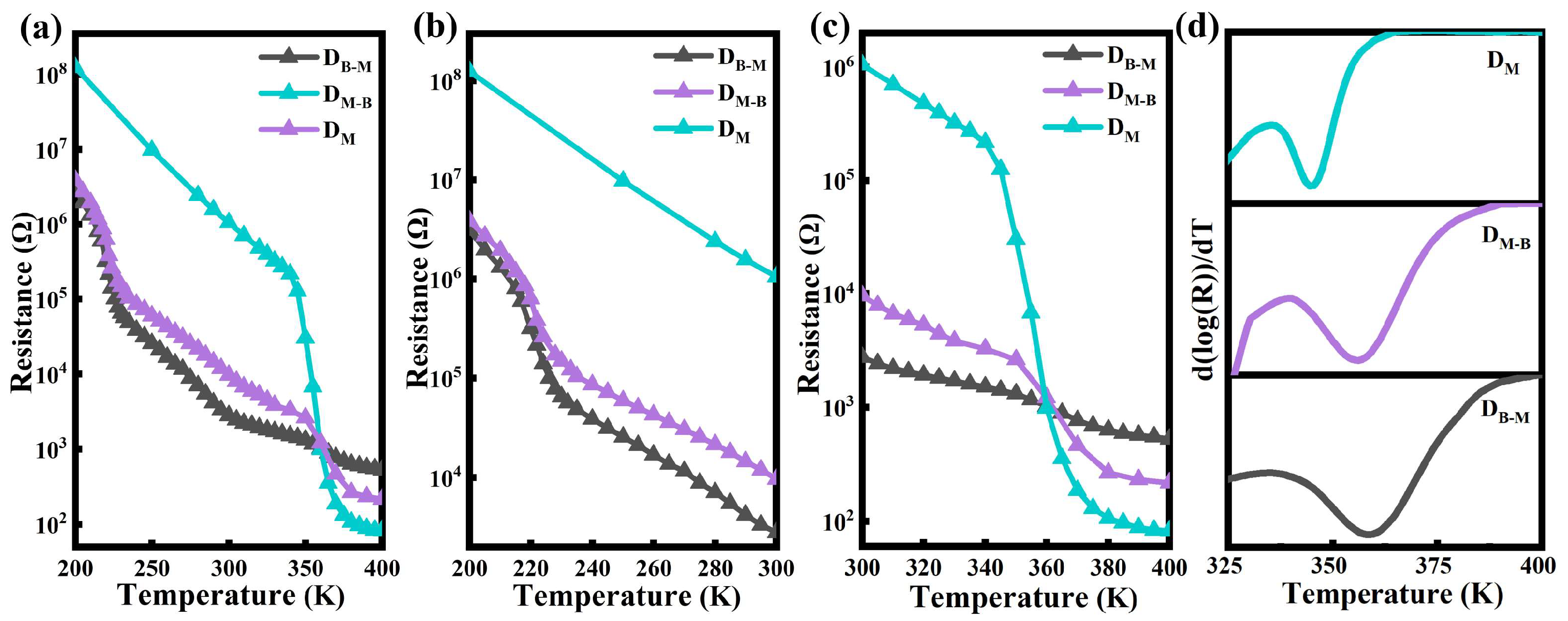
As indicated by the XRD and Raman measurements, the coexistent VO2 (M) and VO2 (B) phases were likely to modify the microstructure and the temperature-dependent structure evolutions. Subsequently, the temperature dependent resistance of the DM, DM-B and DB-M thin films is shown in Figure 5 and Figure S5. The resistance of the DB-M and DM-B thin films changed and underwent a change of over 2 orders of magnitude when the temperature went from 200 K to 300 K, which was related to the IMT process of the VO2 (B) phase [27]. However, no such decrease occurred in the DM thin film, as displayed in Figure 5b. The following drop in the resistance of the DM, DB-M and DM-B thin films at around 350 K was related to VO2 (M) (Figure 5c) [45]. For the DM-B thin film, the small change in resistance from 200 K to 300 K shown in Figure 5b may have resulted from the lower VO2 (B) content and the poorer crystallinity [32]. Figure 5c further suggests the variations in resistance changed from 300 K to 400 K in the DM, DM-B and DB-M thin films [46]. Notably, the increased content of VO2 (B) would have greatly reduced the resistance variations in the as-prepared coexistent VO2 (M) and VO2 (B) thin films from 300 K to 400 K [29]. By taking the derivation curves and using a Gaussian fit, we obtained the transition temperature (TIMT) above room temperature of about 345, 357 and 360 K for the DM, DM-B and DB-M thin films, respectively (Figure 5d). As we obtained in the temperature-dependent Raman spectra, the increased contents of VO2 (B) led to an increase in TIMT [44]. In addition, the TIMT increased with the widened plane spacing from the DM to DM-B and then to DB-M thin films. These results implied that coexistent polymorphs and lattice distortion accompanied and caused such changes in the VO2 thin films with the coexistent VO2 (M) and VO2 (B) phases [45].
3. Conclusions
We have demonstrated the lattice variations and phase-dependent IMT behaviors in the polymorphous thin films with coexistent VO2 (M) and VO2 (B). XRD and Raman measurements revealed that the increased (011)M plane spacing and the red-shifted V-V and V-O vibrations in VO2 (M) were triggered by the presence of more VO2 (B) phases. Temperature-dependent electrical and Raman analyses indicated that increased VO2 (B) phases would promote the transition temperature and reduce the strength of IMT in the polymorphous VO2 thin films. We believe that such a study will contribute to uncovering the coexistent polymorphous phases and the underlying physics behind IMT in VO2 towards advanced electronic and optical devices.
4. Experimental Section
The polymorphous VO2 thin films were obtained with a combination of ALD and post-annealing procedures according to the processes previously reported [31]. The temperature-dependent optical images were obtained via a optical microscope with a home-made heating stage. Raman spectra (Nanofinder 30, Tokyo Instruments, Inc., Tokyo, Japan, the spot size of laser was about 500 nm, power was 1 mW and the grating was 1800 g/mm), micro-XRD (Bruker D8 Discover, Bruker, Karlsruhe, Germany), XRD (Bruker D8, Bruker, Karlsruhe, Germany), X-ray photoelectron spectroscopy (XPS, ESCALAB Xi+, Thermo Fischer Scientific Inc., Waltham, MA, USA) and transmission electron microscopy (TEM, JOEL JEM-2100F, JOEL Ltd., Tokyo, Japan) were used to characterize the VO2 thin films. Electrical curves were recorded at variable temperatures from 77 K to 450 K on a cryogenic probe station (Lakeshore TTPX, Lake Shore Cryotronics, Inc., Woburn, MA, USA) with a semiconductor characterization system (Keithley 2636B, Tektronix, Inc., Beaverton, OR, USA).
Supplementary Materials
The following supporting information can be downloaded at: https://www.mdpi.com/article/10.3390/nano13091514/s1, Figure S1: Optical microscopy images for the DM-B (a) and DB-M (b) thin films at varied temperatures, Figure S2: (a) The V 2p and O 1s XPS spectra and (b) the fitted V 2p XPS spectra for the DM, DM-B and DB-M thin films with coexistent VO2 (M) and VO2 (B) phases, Figure S3: (a) Raman spectra for the polymorphous VO2 thin films with coexistent VO2 (M) and VO2 (B) phases, and details at around 640 cm−1 for the DB-M (b), DM-B (c) and DM (d) thin films, Figure S4: Temperature-dependent Raman spectra for the DB-M (a), DM-B (b) and DM (c) thin films, Figure S5: Temperature-dependent resistance curves and their derivative curves for the DB-M (a), DM-B (b) and DM (c) thin films.
Author Contributions
Conceptualization, X.C. and N.D.; Methodology, M.Q., X.C. and N.D.; Software, M.Q.; Validation, M.Q., W.Y., P.X. and T.H.; Formal analysis, M.Q. and T.H.; Investigation, M.Q.; Resources, X.C. and N.D.; Data curation, M.Q. and P.X.; Writing—original draft, M.Q.; Writing—review & editing, W.Y., T.H., X.C. and N.D.; Project administration, N.D.; Funding acquisition, X.C. and N.D. All authors have read and agreed to the published version of the manuscript.
Funding
This work was funded by NSFC (92064014, 11933006), the National Key R&D Program of China, HZSTB (TD2020002) and Youth Innovation Promotion Association CAS.
Data Availability Statement
Not applicable.
Conflicts of Interest
The authors declare no conflict of interest.
References
- Kalinin, S.V.; Spaldin, N.A. Functional ion defects in transition metal oxides. Science 2013, 341, 858–859. [Google Scholar] [CrossRef] [PubMed]
- Parida, P.; Kashikar, R.; Jena, A.; Nanda, B. Universality in the electronic structure of 3d transition metal oxides. J. Phys. Chem. Solids 2018, 123, 133–149. [Google Scholar] [CrossRef]
- Mizokawa, T.; Fujimori, A. Electronic structure and orbital ordering in perovskite-type 3d transition-metal oxides studied by Hartree-Fock band-structure calculations. Phys. Rev. B 1996, 54, 5368–5380. [Google Scholar] [CrossRef] [PubMed]
- Deka, S. Nanostructured Mixed Transition Metal Oxide Spinels for Supercapacitor Application. Dalton Trans. 2023, 52, 839–856. [Google Scholar] [CrossRef]
- Nandagudi, A.; Nagarajarao, S.H.; Santosh, M.S.; Basavaraja, B.M.; Malode, S.J.; Mascarenhas, R.J.; Shetti, N.P. Hydrothermal synthesis of transition metal oxides, transition metal oxide/carbonaceous material nanocomposites for supercapacitor applications. Mater. Today Sustain. 2022, 19, 100214. [Google Scholar] [CrossRef]
- Zhou, W.; Feng, Z.; Xiong, Y.; Du, G.; Lin, X.; Su, Q.; Lou, Y.; An, S.; You, Y. Visualization of Ferroelectric Domains in Thin Films of Molecular Materials Using Confocal Micro-Raman Spectroscopy. Chem. Res. Chin. Univ. 2022, 38, 1394–1399. [Google Scholar] [CrossRef]
- Li, L.; Zhou, B.; Gao, L.; Jiang, K.; Zhu, L.; Zhang, J.; Hu, Z.; Chu, J. Influence of oxygen partial pressure on the optical properties of β-Ga2O3-δ films deposited by pulsed laser deposition. J. Infrared Millim. W. 2022, 41, 279–284. [Google Scholar]
- Mohammadinejad, A.; Abouzari-Lotf, E.; Aleyaghoob, G.; Rezayi, M.; Oskuee, R.K. Application of a transition metal oxide/carbon-based nanocomposite for designing a molecularly imprinted poly (l-cysteine) electrochemical sensor for curcumin. Food Chem. 2022, 386, 132845. [Google Scholar] [CrossRef]
- Bhardwaj, A.; Kim, I.H.; Hong, J.W.; Kumar, A.; Song, S.J. Transition metal oxide (Ni, Co, Fe)-tin oxide nanocomposite sensing electrodes for a mixed-potential based NO2 sensor. Sens. Actuators B Chem. 2019, 284, 534–544. [Google Scholar] [CrossRef]
- Ahmad, S.; Ayoub, M.H.; Khan, A.M.; Waseem, A.; Yasir, M.; Khan, M.S.; Bajwa, T.M.; Shaikh, A.J. Diverse comparative studies for preferential binding of graphene oxide and transition metal oxide nanoparticles. Colloids Surf. A Physicochem. Eng. Asp. 2022, 647, 129057. [Google Scholar] [CrossRef]
- Ganesamurthi, J.; Shanmugam, R.; Chen, S.M.; Alagumalai, K.; Balamurugan, M.; Yu, Y.Y. Binary transition metal oxide based electrochemical sensor for the evaluation of chlorogenic acid in rea-time samples. Mater. Chem. Phys. 2022, 292, 126757. [Google Scholar] [CrossRef]
- Wang, X.; Gong, X.; Chen, L.; Li, S.; Xie, J.; Liu, Y. Ti3C2 supported transition metal oxides and silver as catalysts toward efficient electricity generation in microbial fuel cells. Catal. Sci. Technol. 2021, 11, 4823–4830. [Google Scholar] [CrossRef]
- Poges, S.; Dutta, B.; Khanna, H.; Moharreri, E.; Aindow, M.; Suib, S.L. Cross Sectional Analysis of Cation Doped Transition Metal Oxide Mesoporous Catalyst Materials. Microsc. Microanal. 2017, 23, 292–293. [Google Scholar] [CrossRef]
- Gu, H.; Lan, J.; Liu, Y.; Ling, C.; Wei, K.; Zhan, G.; Guo, F.; Jia, F.; Ai, Z.; Zhang, L. Water enables lattice oxygen activation of transition metal oxides for volatile organic compound oxidation. ACS Catal. 2022, 12, 11272–11280. [Google Scholar] [CrossRef]
- Ciotonea, C.; Mazilu, I.; Dragoi, B.; Catrinescu, C.; Dumitriu, E.; Ungureanu, A.; Alamdari, H.; Petit, S.; Royer, S. Confining for stability: Heterogeneous catalysis with Transition Metal (Oxide) Nanoparticles confined in the secondary pore network of mesoporous scaffolds. ChemNanoMat 2017, 3, 233–237. [Google Scholar] [CrossRef]
- Mjejri, I.; Etteyeb, N.; Somrani, S.; Sediri, F. Tetragonal pencil-like VO2(R) as electrode materials for high-performance redox activities. Ceram. Int. 2016, 42, 6121–6128. [Google Scholar] [CrossRef]
- Zhang, Y.; Wang, X.; Zhou, Y.; Lai, H.; Liu, P.; Chen, H.; Wang, X.; Xie, W. Highly Sensitive and Ultra-Broadband VO2(B) Photodetector Dominated by Bolometric Effect. Nano Lett. 2021, 22, 485–493. [Google Scholar] [CrossRef]
- Chen, Y.; Ma, S.; Li, X.; Zhao, X.; Cheng, X.; Liu, J. Preparation and microwave absorption properties of microsheets VO2(M). J. Alloy. Compd. 2019, 791, 307–315. [Google Scholar] [CrossRef]
- Strelcov, E.; Lilach, Y.; Kolmakov, A. Gas sensor based on metal-insulator transition in VO2 nanowire thermistor. Nano Lett. 2009, 9, 2322–2326. [Google Scholar] [CrossRef]
- Kasırga, T.S.; Sun, D.; Park, J.H.; Coy, J.M.; Fei, Z.; Xu, X.; Cobden, D.H. Photoresponse of a strongly correlated material determined by scanning photocurrent microscopy. Nat. Nanotechnol. 2012, 7, 723–727. [Google Scholar] [CrossRef]
- Hu, X.; Zhao, Z.; Wang, L.; Li, J.; Wang, C.; Zhao, Y.; Jin, H. VO2(A)/graphene nanostructure: Stand up to Na ion intercalation/deintercalation for enhanced electrochemical performance as a Na-ion battery cathode. Electrochim. Acta 2019, 293, 97–104. [Google Scholar] [CrossRef]
- Polewczyk, V.; Chaluvadi, S.; Orgiani, P.; Panaccione, G.; Vinai, G.; Rossi, G.; Torelli, P. Tuning the magnetic properties of V2O3/CoFeB heterostructures across the V2O3 structural transition. Phys. Rev. Mater. 2021, 5, 034413. [Google Scholar] [CrossRef]
- Mazzola, F.; Chaluvadi, S.K.; Polewczyk, V.; Mondal, D.; Fujii, J.; Rajak, P.; Islam, M.; Ciancio, R.; Barba, L.; Fabrizio, M. Disentangling Structural and Electronic Properties in V2O3 Thin Films: A Genuine Nonsymmetry Breaking Mott Transition. Nano Lett. 2022, 22, 5990–5996. [Google Scholar] [CrossRef] [PubMed]
- Morin, F. Oxides which show a metal-to-insulator transition at the Neel temperature. Phys. Rev. Lett. 1959, 3, 34–36. [Google Scholar] [CrossRef]
- Rodríguez, L.; Sandiumenge, F.; Frontera, C.; Caicedo, J.M.; Padilla, J.; Catalán, G.; Santiso, J. Strong strain gradients and phase coexistence at the metal-insulator transition in VO2 epitaxial films. Acta Mater. 2021, 220, 117336. [Google Scholar] [CrossRef]
- Choi, S.; Son, J.; Oh, J.; Lee, J.-H.; Jang, J.H.; Lee, S. Sharp contrast in the electrical and optical properties of vanadium Wadsley (VmO2m+1, m>1) epitaxial films selectively stabilized on (111)-oriented Y-stabilized ZrO2. Phys. Rev. Mater. 2019, 3, 063401. [Google Scholar] [CrossRef]
- Kumar, M.; Kim, Y.; Lee, H.H. Temperature dependent structural, electrical and electronic investigation of VO2(B) thin film. Curr. Appl. Phys. 2021, 30, 85–90. [Google Scholar] [CrossRef]
- Choi, S.; Chang, S.J.; Oh, J.; Jang, J.H.; Lee, S. Electrical and Optical Properties of VO2 Polymorphic Films Grown Epitaxially on Y-Stabilized ZrO2. Adv. Electron. Mater. 2018, 4, 1700620. [Google Scholar] [CrossRef]
- Majid, S.S.; Ahad, A.; Rahman, F.; Sathe, V.; Shukla, D. Unveiling the Role of VO2(B) Polymorph in the Insulator-Metal Transition of VO2(M1) Thin Films. Phys. Status Solidi B 2022, 259, 2200108. [Google Scholar] [CrossRef]
- Wentzcovitch, R.M.; Schulz, W.W.; Allen, P.B. VO2: Peierls or Mott-Hubbard? A view from band theory. Phys. Rev. Lett. 1994, 72, 3389–3392. [Google Scholar] [CrossRef]
- Wang, S.; Wei, W.; Huang, T.; Zhang, T.; Chen, Z.; Chen, X.; Dai, N. Nonstoichiometric Oxygen-Dependent Microstructures and Phase Transitions in Post-Annealed Vanadium Dioxides. Adv. Eng. Mater. 2019, 21, 1801374. [Google Scholar] [CrossRef]
- Gu, D.; Li, Y.; Zhou, X.; Xu, Y. Facile fabrication of composite vanadium oxide thin films with enhanced thermochromic properties. ACS Appl. Mater. Interfaces 2019, 11, 37617–37625. [Google Scholar] [CrossRef] [PubMed]
- Wang, S.; Wei, W.; Huang, T.; Yuan, M.; Yang, Y.; Yang, W.; Zhang, R.; Zhang, T.; Chen, Z.; Chen, X. Al-Doping-Induced VO2(B) Phase in VO2(M) Toward Smart Optical Thin Films with Modulated ΔTvis and ΔTc. Adv. Eng. Mater. 2019, 21, 1900947. [Google Scholar] [CrossRef]
- Chen, A.; Bi, Z.; Zhang, W.; Jian, J.; Jia, Q.; Wang, H. Textured metastable VO2(B) thin films on SrTiO3 substrates with significantly enhanced conductivity. Appl. Phys. Lett. 2014, 104, 071909. [Google Scholar] [CrossRef]
- Humphreys, C. The significance of Bragg’s law in electron diffraction and microscopy, and Bragg’s second law. Acta Crystallogr. A Found. Adv. 2013, 69, 45–50. [Google Scholar] [CrossRef]
- Liu, H.; Wan, D.; Ishaq, A.; Chen, L.; Guo, B.; Shi, S.; Luo, H.; Gao, Y. Sputtering deposition of sandwich-structured V2O5/metal (V, W)/V2O5 multilayers for the preparation of high-performance thermally sensitive VO2 thin films with selectivity of VO2(B) and VO2(M) polymorph. ACS Appl. Mater. Interfaces 2016, 8, 7884–7890. [Google Scholar] [CrossRef]
- Leroux, C.; Nihoul, G.; Van Tendeloo, G. From VO2(B) to VO2(R): Theroretical structures of VO2 polymorphs and in situ electron microscopy. Phys. Rev. B 1999, 57, 5111–5121. [Google Scholar] [CrossRef]
- Biesinger, M.C.; Payne, B.P.; Grosvenor, A.P.; Lau, L.W.; Gerson, A.R.; Smart, R.S.C. Resolving surface chemical states in XPS analysis of first row transition metals, oxides and hydroxides: Cr, Mn, Fe, Co and Ni. Appl. Surf. Sci. 2011, 257, 2717–2730. [Google Scholar] [CrossRef]
- Miao, P.; Wu, J.; Du, Y.; Sun, Y.; Xu, P. Phase transition induced Raman enhancement on vanadium dioxide (VO2) nanosheets. J. Mater. Chem. C 2018, 6, 10855–10860. [Google Scholar] [CrossRef]
- Shvets, P.; Dikaya, O.; Maksimova, K.; Goikhman, A. A review of Raman spectroscopy of vanadium oxides. J. Raman Spectrosc. 2019, 50, 1226–1244. [Google Scholar] [CrossRef]
- Shi, R.; Chen, Y.; Cai, X.; Lian, Q.; Zhang, Z.; Shen, N.; Amini, A.; Wang, N.; Cheng, C. Phase management in single-crystalline vanadium dioxide beams. Nat. Commun. 2021, 12, 34244501. [Google Scholar] [CrossRef]
- Bersani, D.; Lottici, P.; Montenero, A. Micro-Raman investigation of iron oxide films and powders produced by sol-gel syntheses. J. Raman Spectrosc. 1999, 30, 355–360. [Google Scholar] [CrossRef]
- Lee, S.; Sun, X.-G.; Lubimtsev, A.A.; Gao, X.; Ganesh, P.; Ward, T.Z.; Eres, G.; Chisholm, M.F.; Dai, S.; Lee, H.N. Persistent electrochemical performance in epitaxial VO2(B). Nano Lett. 2017, 17, 2229–2233. [Google Scholar] [CrossRef]
- Oka, Y.; Yao, T.; Yamamoto, N.; Ueda, Y.; Hayashi, A. Phase transition and V4+-V4+ pairing in VO2 (B). J. Solid State Chem. 1993, 105, 271–278. [Google Scholar] [CrossRef]
- Muraoka, Y.; Hiroi, Z. Metal-insulator transition of VO2 thin films grown on TiO2 (001) and (110) substrates. Appl. Phys. Lett. 2002, 80, 583–585. [Google Scholar] [CrossRef]
- Émond, N.; Torriss, B.; Chaker, M. Natural and induced growth of VO2 (M) on VO2 (B) ultrathin films. Sci. Rep. 2018, 8, 7153. [Google Scholar] [CrossRef]
Figure 1.
(a) TEM cross-section image and (b) XRD pattern for the VO2 thin films with coexistent VO2 (M) and VO2 (B) phases, and magnified TEM images for (c) VO2 (M) and (d) VO2 (B) phases.
Figure 1.
(a) TEM cross-section image and (b) XRD pattern for the VO2 thin films with coexistent VO2 (M) and VO2 (B) phases, and magnified TEM images for (c) VO2 (M) and (d) VO2 (B) phases.

Figure 2.
(a) XRD patterns, (b) fitted XRD patterns, and (c) XPS spectra for the DM, DM-B and DB-M thin films with coexistent VO2 (M) and VO2 (B) phases.
Figure 2.
(a) XRD patterns, (b) fitted XRD patterns, and (c) XPS spectra for the DM, DM-B and DB-M thin films with coexistent VO2 (M) and VO2 (B) phases.

Figure 3.
(a) Raman spectra at around 194 cm−1 (the blue dashed box in (b)), (b) line-scanned Raman mapping and (c) Raman spectra at around 640 cm−1 (the yellow dashed box in (b)) in the DB-M, DM-B and DM thin films. The blue and yellow dashed lines were used to show the position variations of Raman peaks at around 195 and 620 cm−1 among the DB-M, DM-B and DM thin films, respectively.

Figure 4.
Temperature-dependent Raman modes at around (a) 191 and (a’) 403 cm−1 for the DB-M thin film. Temperature-dependent (b) ωV1 and (b’) ωV-O modes for the DM-B thin film, and temperature-dependent (c) ωV1 and (c’) ωV-O modes for the DM thin film.
Figure 4.
Temperature-dependent Raman modes at around (a) 191 and (a’) 403 cm−1 for the DB-M thin film. Temperature-dependent (b) ωV1 and (b’) ωV-O modes for the DM-B thin film, and temperature-dependent (c) ωV1 and (c’) ωV-O modes for the DM thin film.

Figure 5.
(a) Temperature-dependent resistance curves for the DM, DM-B and DB-M thin films during a heating process. The resistance–temperature curves in the temperature range of (b) 200–300 K and (c) 300–400 K, and (d) the derivation curves for calculating TIMT for the DM, DM-B and DB-M thin films.

Disclaimer/Publisher’s Note: The statements, opinions and data contained in all publications are solely those of the individual author(s) and contributor(s) and not of MDPI and/or the editor(s). MDPI and/or the editor(s) disclaim responsibility for any injury to people or property resulting from any ideas, methods, instructions or products referred to in the content. |
© 2023 by the authors. Licensee MDPI, Basel, Switzerland. This article is an open access article distributed under the terms and conditions of the Creative Commons Attribution (CC BY) license (https://creativecommons.org/licenses/by/4.0/).
Share and Cite
MDPI and ACS Style
Qiu, M.; Yang, W.; Xu, P.; Huang, T.; Chen, X.; Dai, N. Coexistent VO2 (M) and VO2 (B) Polymorphous Thin Films with Multiphase-Driven Insulator–Metal Transition. Nanomaterials 2023, 13, 1514. https://doi.org/10.3390/nano13091514
AMA Style
Qiu M, Yang W, Xu P, Huang T, Chen X, Dai N. Coexistent VO2 (M) and VO2 (B) Polymorphous Thin Films with Multiphase-Driven Insulator–Metal Transition. Nanomaterials. 2023; 13(9):1514. https://doi.org/10.3390/nano13091514
Chicago/Turabian StyleQiu, Mengxia, Wanli Yang, Peiran Xu, Tiantian Huang, Xin Chen, and Ning Dai. 2023. "Coexistent VO2 (M) and VO2 (B) Polymorphous Thin Films with Multiphase-Driven Insulator–Metal Transition" Nanomaterials 13, no. 9: 1514. https://doi.org/10.3390/nano13091514
Note that from the first issue of 2016, this journal uses article numbers instead of page numbers. See further details here.