
Structure Formation and Regulation of Au Nanoparticles in LiTaO3 by Ion Beam and Thermal Annealing Techniques

 and
and 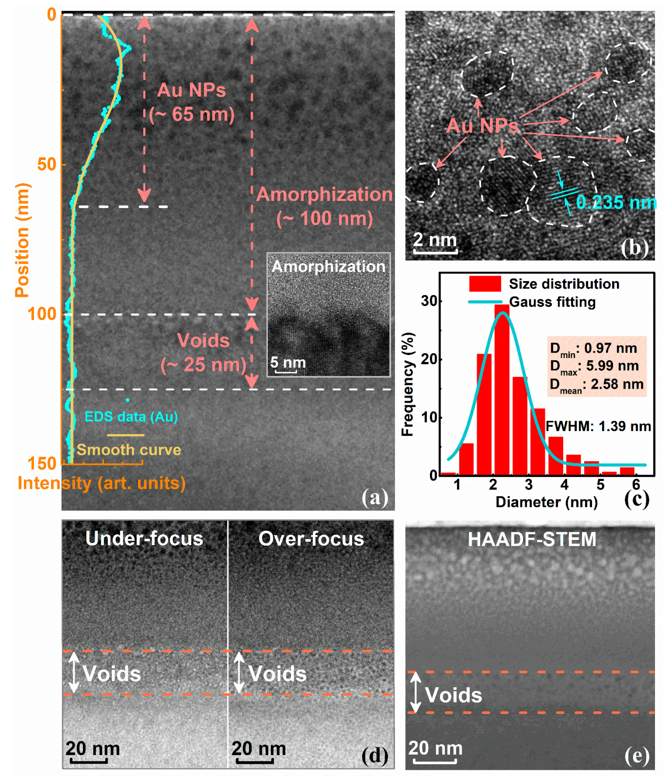
Abstract
:1. Introduction
2. Materials and Methods
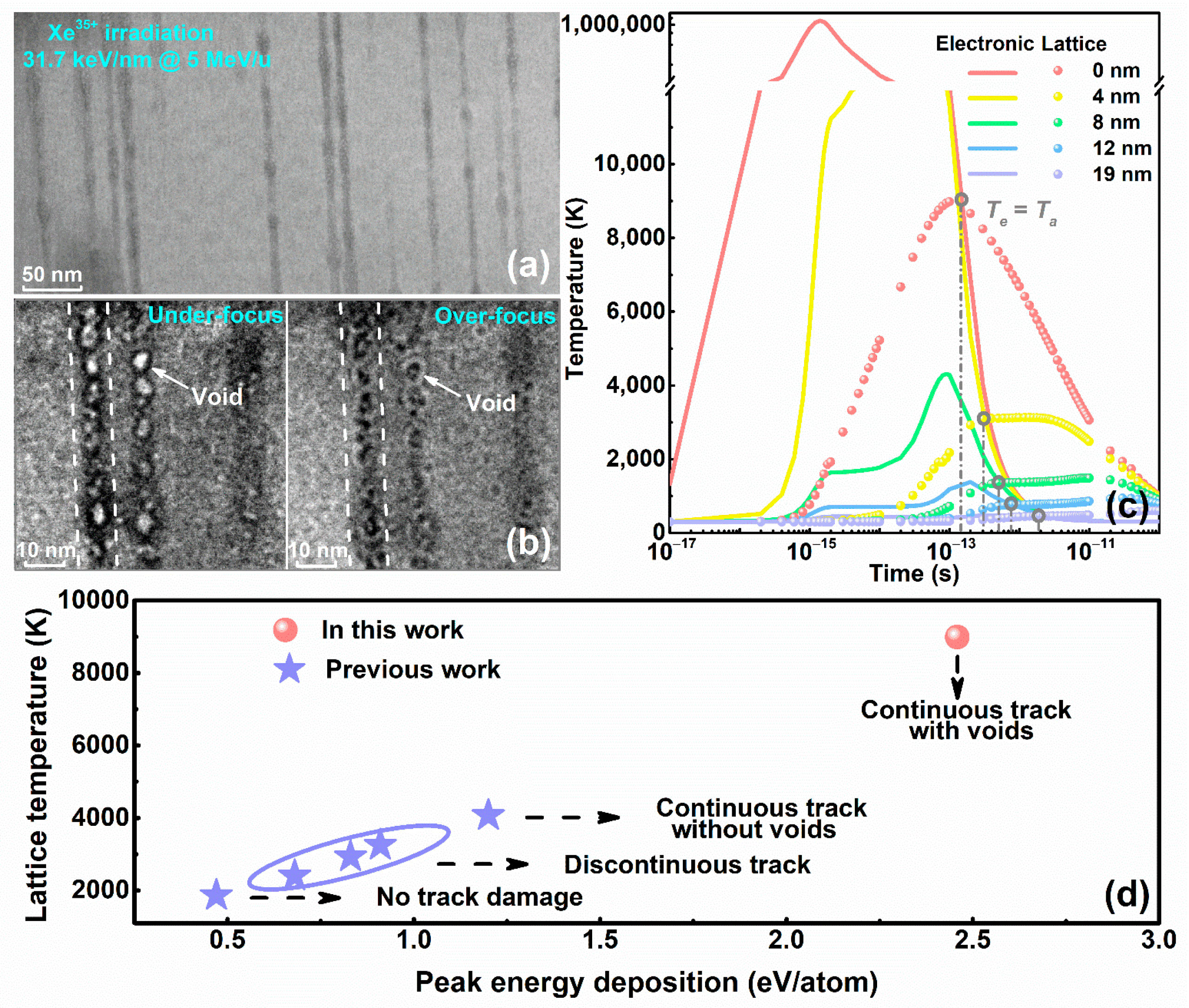
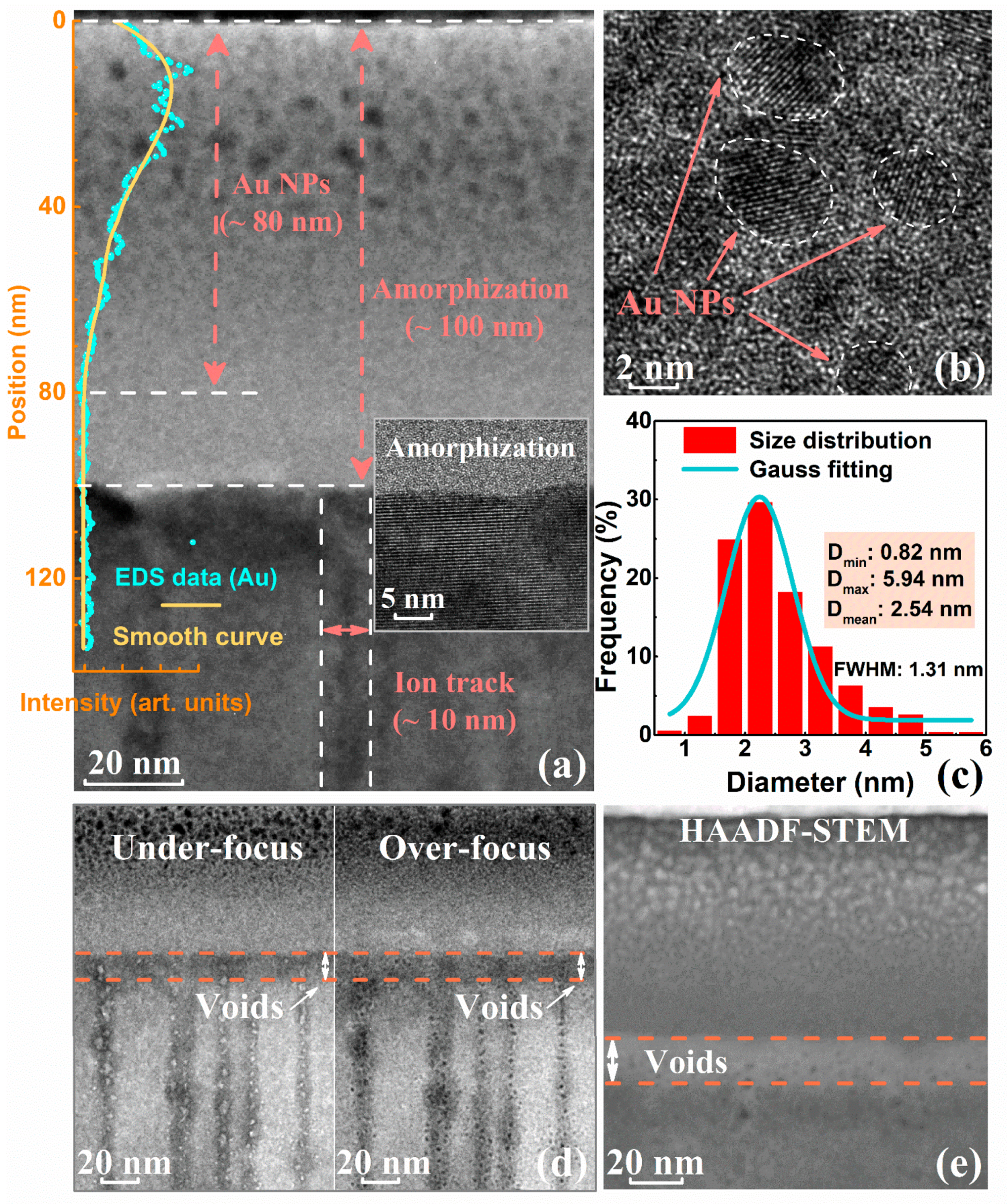
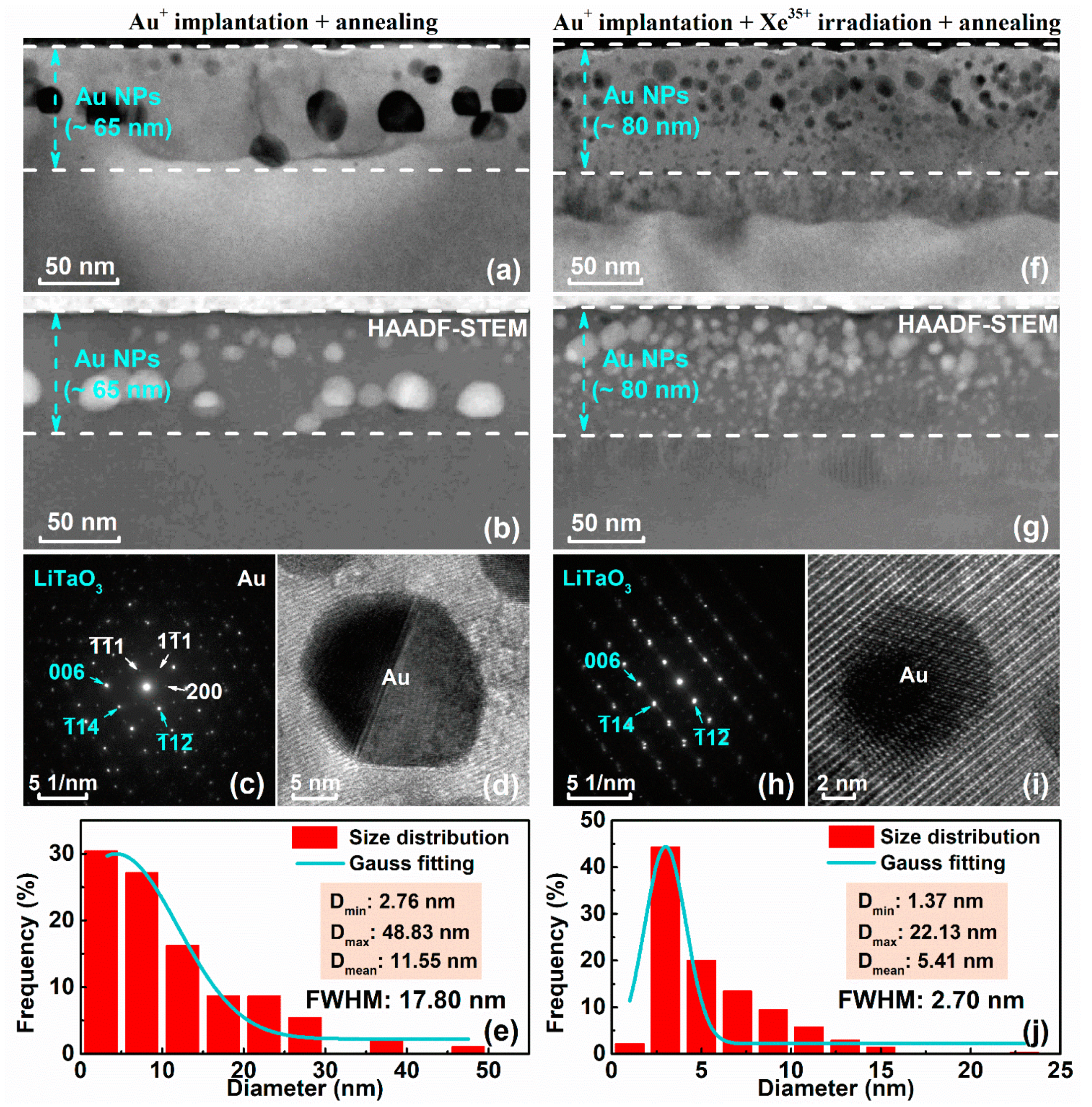
3. Results and Discussion
4. Conclusions
Author Contributions
Funding
Data Availability Statement
Acknowledgments
Conflicts of Interest
References
- Nie, W.J.; Zhang, Y.X.; Yu, H.H.; Li, R.; He, R.Y.; Dong, N.N.; Wang, J.; Hübner, R.; Böttger, R.; Zhou, S.Q.; et al. Plasmonic nanoparticles embedded in single crystals synthesized by gold ion implantation for enhanced optical nonlinearity and efficient Q-switched lasing. Nanoscale 2018, 10, 4228–4236. [Google Scholar] [CrossRef] [PubMed] [Green Version]
- Zhou, L.; Mao, J.Y.; Ren, Y.; Yang, J.Q.; Zhang, S.R.; Zhou, Y.; Liao, Q.; Zeng, Y.J.; Shan, H.; Xu, Z.; et al. Biological spiking synapse constructed from solution processed bimetal core-shell nanoparticle based composites. Small 2018, 14, 1800288. [Google Scholar] [CrossRef] [PubMed]
- Franco-Ulloa, S.; Tatulli, G.; Bore, S.L.; Moglianetti, M.; Pompa, P.P.; Cascella, M.; De Vivo, M. Dispersion state phase diagram of citrate-coated metallic nanoparticles in saline solutions. Nat. Commun. 2020, 11, 5422. [Google Scholar] [CrossRef] [PubMed]
- Tagliabue, G.; DuChene, J.S.; Abdellah, M.; Habib, A.; Gosztola, D.J.; Hattori, Y.; Cheng, W.H.; Zheng, K.; Canton, S.E.; Sundararaman, R.; et al. Ultrafast hot-hole injection modifies hot-electron dynamics in Au/p-GaN heterostructures. Nat. Mater. 2020, 19, 1312–1318. [Google Scholar] [CrossRef]
- Zhao, X.; Tu, B.; Li, M.; Feng, X.; Zhang, Y.; Fang, Q.; Li, T.; Grzybowski, B.A.; Yan, Y. Switchable counterion gradients around charged metallic nanoparticles enable reception of radio waves. Sci. Adv. 2018, 4, eaau3546. [Google Scholar] [CrossRef] [Green Version]
- Dean, J.; Taylor, M.G.; Mpourmpakis, G. Unfolding adsorption on metal nanoparticles: Connecting stability with catalysis. Sci. Adv. 2019, 5, eaax5101. [Google Scholar] [CrossRef] [Green Version]
- Liu, Y.; Liu, S.; Chen, R.; Zhan, W.; Ni, H.; Liang, F. An antibacterial nonenzymatic glucose sensor composed of carbon nanotubes decorated with silver nanoparticles. Electroanalysis 2015, 27, 1138–1143. [Google Scholar] [CrossRef]
- Yang, A.H.; Moore, S.D.; Schmidt, B.S.; Klug, M.; Lipson, M.; Erickson, D. Optical manipulation of nanoparticles and biomolecules in sub-wavelength slot waveguides. Nature 2009, 457, 71–75. [Google Scholar] [CrossRef]
- Carles, R.; Bayle, M.; Benzo, P.; Benassayag, G.; Bonafos, C.; Cacciato, G.; Privitera, V. Plasmon-resonant Raman spectroscopy in metallic nanoparticles: Surface-enhanced scattering by electronic excitations. Phys. Rev. B 2015, 92, 174302. [Google Scholar] [CrossRef] [Green Version]
- Choi, J.H.; Choi, J.W. Metal-enhanced fluorescence by bifunctional Au nanoparticles for highly sensitive and simple detection of proteolytic enzyme. Nano Lett. 2020, 20, 7100–7107. [Google Scholar] [CrossRef]
- Stepanov, A.L.S. Synthesis of silver nanoparticles in dielectric matrix by ion implantation: A review. Rev. Adv. Mater. Sci. 2010, 26, 1–29. [Google Scholar]
- Bogani, L.; Cavigli, L.; de Julián Fernández, C.; Mazzoldi, P.; Mattei, G.; Gurioli, M.; Dressel, M.; Gatteschi, D. Photocoercivity of Nano-Stabilized Au: Fe Superparamagnetic Nanoparticles. Adv. Mater. 2010, 22, 4054–4058. [Google Scholar] [CrossRef] [PubMed]
- Can-Uc, B.; Rangel-Rojo, R.; Peña-Ramírez, A.; de Araújo, C.B.; Baltar, H.T.M.C.M.; Crespo-Sosa, A.; Garcia-Betancourt, M.L.; Oliver, A. Nonlinear optical response of platinum nanoparticles and platinum ions embedded in sapphire. Opt. Express 2016, 24, 9955–9965. [Google Scholar] [CrossRef] [PubMed]
- Roorda, S.; van Dillen, T.; Polman, A.; Graf, C.; van Blaaderen, A.; Kooi, B.J. Aligned gold nanorods in silica made by ion irradiation of core-shell colloidal particles. Adv. Mater. 2004, 16, 235–237. [Google Scholar] [CrossRef] [Green Version]
- Leveneur, J.; Waterhouse, G.I.; Kennedy, J.; Metson, J.B.; Mitchell, D.R. Nucleation and growth of Fe nanoparticles in SiO2: A TEM, XPS, and Fe L-edge XANES investigation. J. Phys. Chem. C 2011, 115, 20978–20985. [Google Scholar] [CrossRef]
- Wolf, S.; Rensberg, J.; Johannes, A.; Thomae, R.; Smit, F.; Neveling, R.; Moodley, M.; Bierschenk, T.; Rodriguez, M.; Afra, B.; et al. Shape manipulation of ion irradiated Ag nanoparticles embedded in lithium niobate. Nanotechnology 2016, 27, 145202. [Google Scholar] [CrossRef]
- Pang, C.; Li, R.; Li, Z.; Dong, N.; Wang, J.; Ren, F.; Chen, F. Plasmonic Ag nanoparticles embedded in lithium tantalate crystal for ultrafast laser generation. Nanotechnology 2019, 30, 334001. [Google Scholar] [CrossRef]
- Carles, R.; Farcău, C.; Bonafos, C.; Benassayag, G.; Pécassou, B.; Zwick, A. The synthesis of single layers of Ag nanocrystals by ultra-low-energy ion implantation for large-scale plasmonic structures. Nanotechnology 2009, 20, 355305. [Google Scholar] [CrossRef]
- Kishimoto, N.; Umeda, N.; Takeda, Y.; Gritsyna, V.T.; Renk, T.J.; Thompson, M.O. In-beam growth and rearrangement of nanoparticles in insulators induced by high-current negative copper ions. Vacuum 2000, 58, 60–78. [Google Scholar] [CrossRef]
- Ramaswamy, V.; Haynes, T.E.; White, C.W.; MoberlyChan, W.J.; Roorda, S.; Aziz, M.J. Synthesis of nearly monodisperse embedded nanoparticles by separating nucleation and growth in ion implantation. Nano Lett. 2005, 5, 373–377. [Google Scholar] [CrossRef]
- Valentin, E.; Bernas, H.; Ricolleau, C.; Creuzet, F. Ion Beam “Photography”: Decoupling nucleation and growth of metal clusters in glass. Phys. Rev. Lett. 2001, 86, 99. [Google Scholar] [CrossRef] [PubMed]
- Song, H.; Yu, X.; Chen, M.; Qiao, M.; Wang, T.; Zhang, J.; Liu, Y.; Liu, P.; Wang, X. Modification of WS2 nanosheets with controllable layers via oxygen ion irradiation. Appl. Surf. Sci. 2018, 439, 240–245. [Google Scholar] [CrossRef]
- Liu, Y.; Crespillo, M.L.; Huang, Q.; Wang, T.J.; Liu, P.; Wang, X.L. Lattice damage assessment and optical waveguide properties in LaAlO3 single crystal irradiated with swift Si ions. J. Phys. D 2017, 50, 055303. [Google Scholar] [CrossRef]
- Zhao, J.H.; Huang, Q.; Liu, P.; Wang, X.L. An He-implanted optical planar waveguide in an Nd: YGG laser crystal preserving fluorescence properties. Appl. Surf. Sci. 2011, 257, 7310–7313. [Google Scholar] [CrossRef]
- Liu, T.; Liu, P.; Zhang, L.; Zhou, Y.F.; Yu, X.F.; Zhao, J.H.; Wang, X.L. Visible and near-infrared planar waveguide structure of polycrystalline zinc sulfide from C ions implantation. Opt. Express 2013, 21, 4671–4676. [Google Scholar] [CrossRef] [PubMed]
- Liu, Y.; Huang, Q.; Crespillo, M.L.; Qiao, M.; Liu, P.; Wang, X.L. Ion beam damage assessment and waveguide formation induced by energetic Si-ion irradiation in lanthanum aluminate crystal. Opt. Mater. 2017, 64, 391–400. [Google Scholar] [CrossRef]
- Liu, H.; Zhang, X.; Shen, Y.; Zhang, L.; Wang, J.; Zhu, F.; Zhang, B.; Liu, C. Tailoring the size distribution of Ag nanoparticles embedded in SiO2 by Xe ion postirradiation. Appl. Phys. Express 2012, 5, 105002. [Google Scholar] [CrossRef]
- Giulian, R.; Kluth, P.; Araujo, L.L.; Llewellyn, D.J.; Ridgway, M.C. Pt nanocrystals formed by ion implantation: A defect-mediated nucleation process. Appl. Phys. Lett. 2007, 91, 093115. [Google Scholar] [CrossRef] [Green Version]
- D’Orléans, C.; Stoquert, J.P.; Estournes, C.; Cerruti, C.; Grob, J.J.; Guille, J.L.; Haas, F.; Muller, D.; Richard-Plouet, M. Publisher’s Note: Anisotropy of Co nanoparticles induced by swift heavy ions. Phys. Rev. B 2003, 67, 220101. [Google Scholar] [CrossRef]
- Kluth, P.; Schnohr, C.S.; Pakarinen, O.H.; Djurabekova, F.; Sprouster, D.J.; Giulian, R.; Ridgway, M.C.; Byrne, A.P.; Trautmann, C.; Cookson, D.J.; et al. Fine structure in swift heavy ion tracks in amorphous SiO2. Phys. Rev. Lett. 2008, 101, 175503. [Google Scholar] [CrossRef] [Green Version]
- Liu, Y.; Han, X.; Crespillo, M.L.; Huang, Q.; Liu, P.; Wang, X. Ion tracks formation through synergistic energy processes in strontium titanate under swift heavy ion irradiation: Experimental and theoretical approaches. Materialia 2019, 7, 100402. [Google Scholar] [CrossRef]
- Ridgway, M.C.; Giulian, R.; Sprouster, D.J.; Kluth, P.; Araújo, L.L.; Llewellyn, D.J.; Byrne, A.P.; Kremer, F.; Fichtner, P.F.P.; Rizza, G. Role of thermodynamics in the hape transformation of embedded metal nanoparticles induced by swift heavy-ion irradiation. Phys. Rev. Lett. 2011, 106, 095505. [Google Scholar] [CrossRef] [PubMed] [Green Version]
- Zhang, Y.; Lian, J.; Zhu, Z.; Bennett, W.D.; Saraf, L.V.; Rausch, J.L.; Hendricks, C.A.; Ewing, R.C.; Weber, W.J. Response of strontium titanate to ion and electron irradiation. J. Nucl. Mater. 2009, 389, 303–310. [Google Scholar] [CrossRef]
- Ziegler, J.F.; Ziegler, M.D.; Biersack, J.P. SRIM–The stopping and range of ions in matter. Nucl. Instrum. Methods Phys. Res. Sect. 2010, 268, 1818–1823. [Google Scholar] [CrossRef] [Green Version]
- Toulemonde, M.; Assmann, W.; Dufour, C.; Meftah, A.; Studer, F.; Trautmann, C. Experimental phenomena and thermal spike model description of ion tracks in amorphisable inorganic insulators. Mat. Fys. Medd. 2006, 52, 263–292. [Google Scholar]
- Liu, Y.; Han, X.; Huang, Q.; Crespillo, M.L.; Liu, P.; Zarkadoula, E.; Wang, X. Structural damage response of lanthanum and yttrium aluminate crystals to nuclear collisions and electronic excitation: Threshold assessment of irradiation damage. J. Mater. Sci. Technol. 2021, 90, 95–107. [Google Scholar] [CrossRef]
- Waligorski, M.P.R.; Hamm, R.N.; Katz, R. The radial distribution of dose around the path of a heavy ion in liquid water. Nucl. Tracks Radiat. Meas. 1986, 11, 309–319. [Google Scholar] [CrossRef] [Green Version]
- Baranov, I.A.; Martynenko, Y.V.; Tsepelevich, S.O.; Yavlinskiĭ, Y.N. Inelastic sputtering of solids by ions. Sov. Phys. Usp. 1988, 31, 1015. [Google Scholar] [CrossRef]
- Toulemonde, M.; Trautmann, C.; Balanzat, E.; Hjort, K.; Weidinger, A. Track formation and fabrication of nanostructures with MeV-ion beams. Nucl. Instrum. Methods Phys. Res. 2004, 216, 1–8. [Google Scholar] [CrossRef]
- Assmann, W.; Toulemonde, M.; Trautmann, C. Electronic sputtering with swift heavy ions. In Sputtering by Particle Bombardment; Springer: Berlin/Heidelberg, Germany, 2007; pp. 401–450. [Google Scholar]
- Toulemonde, M.; Dufour, C.; Paumier, E. Transient thermal process after a high-energy heavy-ion irradiation of amorphous metals and semiconductors. Phys. Rev. B 1992, 46, 14362. [Google Scholar] [CrossRef]
- Han, X.; Liu, Y.; Huang, Q.; Crespillo, M.L.; Liu, P.; Wang, X. Swift heavy ion tracks in alkali tantalate crystals: A combined experimental and computational study. J. Phys. D Appl. Phys. 2020, 53, 105304. [Google Scholar] [CrossRef]
- Wang, Y.Q.; Liang, W.S.; Geng, C.Y. Coalescence behavior of gold nanoparticles. Nanoscale Res. Lett. 2009, 4, 684–688. [Google Scholar] [CrossRef] [PubMed]
- Han, X.; Liu, Y.; Crespillo, M.L.; Zarkadoula, E.; Huang, Q.; Wang, X.; Liu, P. Latent tracks in ion-irradiated LiTaO3 crystals: Damage morphology characterization and thermal spike analysis. Crystal 2020, 10, 877. [Google Scholar] [CrossRef]
- Dufour, C.; Khomenkov, V.; Rizza, G.; Toulemonde, M. Ion-matter interaction: The three-dimensional version of the thermal spike model. Application to nanoparticle irradiation with swift heavy ions. J. Phys. D 2012, 45, 065302. [Google Scholar] [CrossRef] [Green Version]
- Singh, S.K.; Singhal, R. Thermal annealing and SHI irradiation induced modifications in sandwiched structured Carbon-gold-Carbon (a-C/Au/a-C) nanocomposite thin film. Nucl. Instrum. Methods Phys. Res. Sect. B 2017, 407, 118–124. [Google Scholar] [CrossRef]
- Zhang, X.D.; Xi, J.F.; Shen, Y.Y.; Zhang, L.H.; Zhu, F.; Wang, Z.; Xue, Y.H.; Liu, C.L. Thermal evolution and optical properties of Cu nanoparticles in SiO2 by ion implantation. Opt. Mater. 2011, 33, 570–575. [Google Scholar] [CrossRef]


Publisher’s Note: MDPI stays neutral with regard to jurisdictional claims in published maps and institutional affiliations. |
© 2022 by the authors. Licensee MDPI, Basel, Switzerland. This article is an open access article distributed under the terms and conditions of the Creative Commons Attribution (CC BY) license (https://creativecommons.org/licenses/by/4.0/).
Share and Cite
Liu, Y.; Han, X.; Zhao, J.; Sun, J.; Huang, Q.; Wang, X.; Liu, P. Structure Formation and Regulation of Au Nanoparticles in LiTaO3 by Ion Beam and Thermal Annealing Techniques. Nanomaterials 2022, 12, 4028. https://doi.org/10.3390/nano12224028
Liu Y, Han X, Zhao J, Sun J, Huang Q, Wang X, Liu P. Structure Formation and Regulation of Au Nanoparticles in LiTaO3 by Ion Beam and Thermal Annealing Techniques. Nanomaterials. 2022; 12(22):4028. https://doi.org/10.3390/nano12224028
Chicago/Turabian StyleLiu, Yong, Xinqing Han, Jinhua Zhao, Jian Sun, Qing Huang, Xuelin Wang, and Peng Liu. 2022. "Structure Formation and Regulation of Au Nanoparticles in LiTaO3 by Ion Beam and Thermal Annealing Techniques" Nanomaterials 12, no. 22: 4028. https://doi.org/10.3390/nano12224028