
Effect of Cu Intercalation Layer on the Enhancement of Spin-to-Charge Conversion in Py/Cu/Bi2Se3
 ,
, 
Abstract
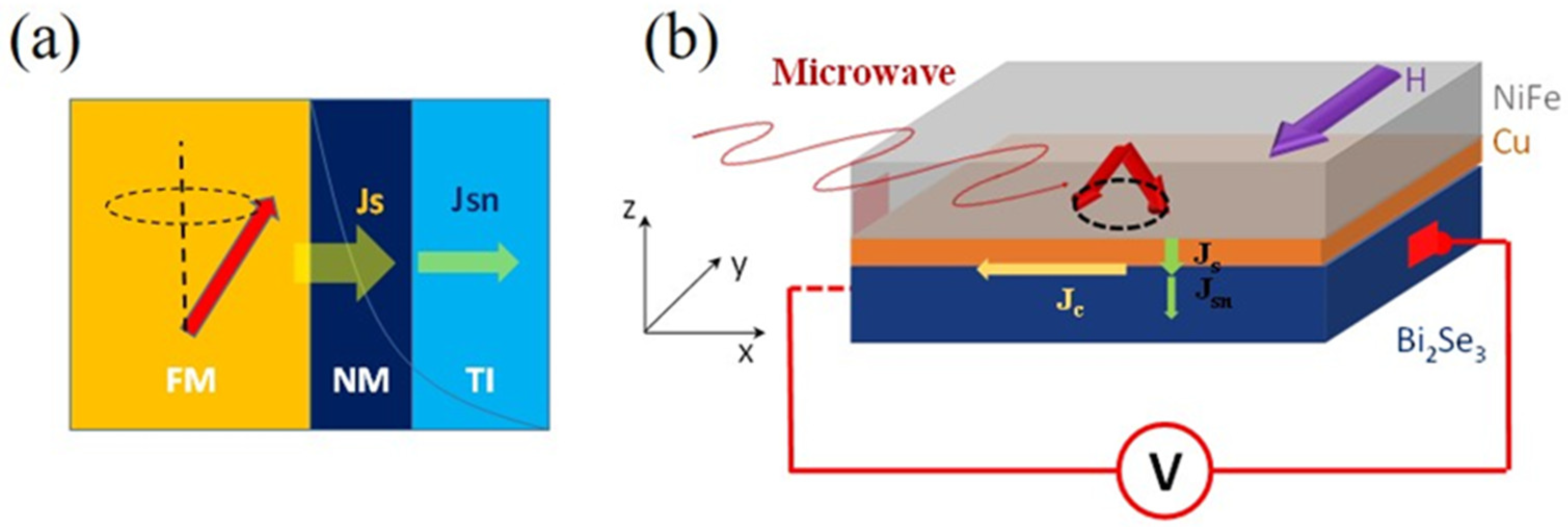
:1. Introduction
2. Experimental
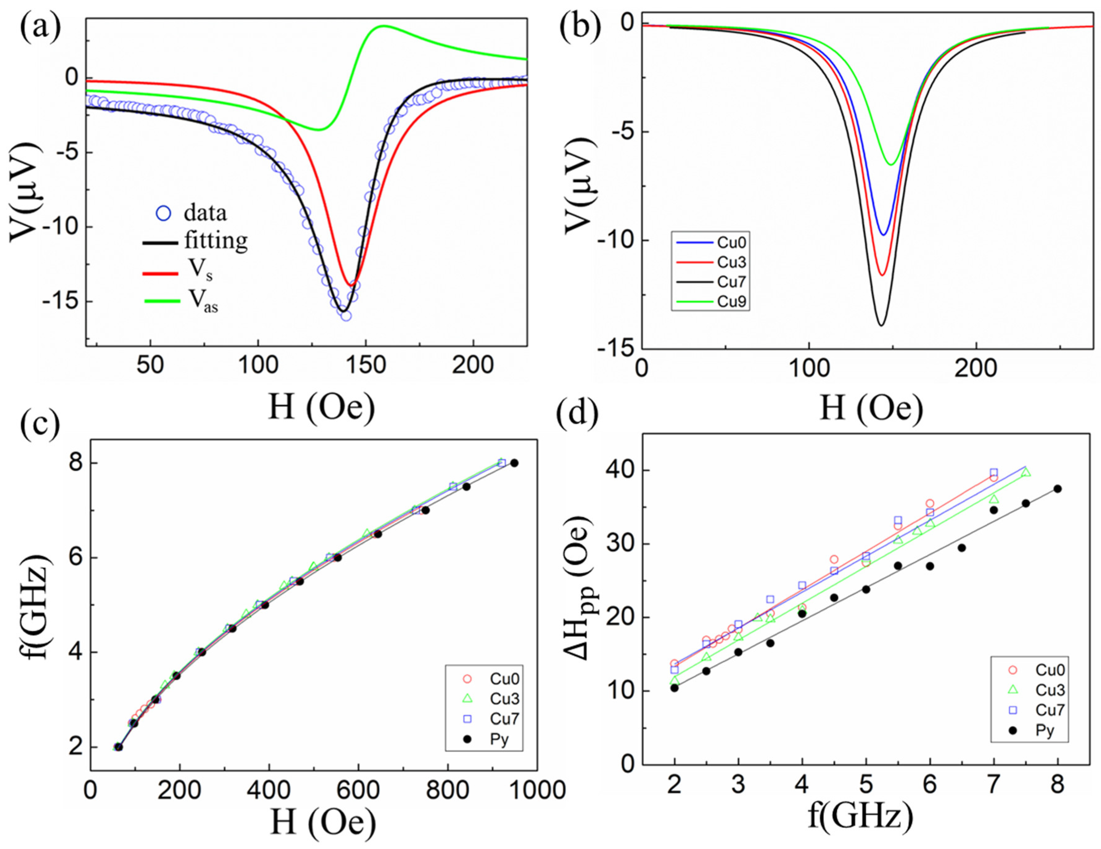
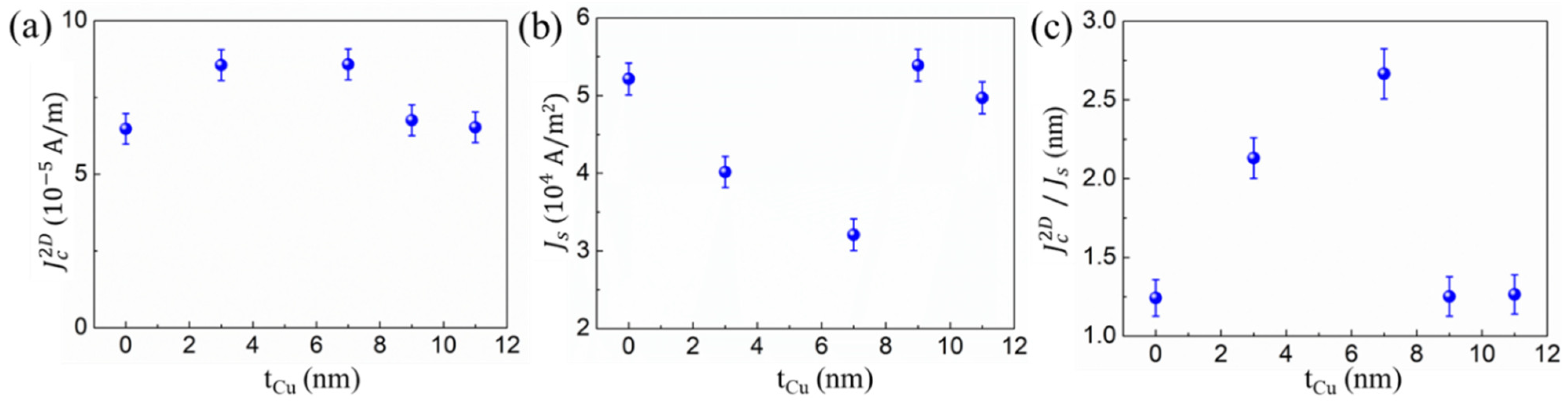
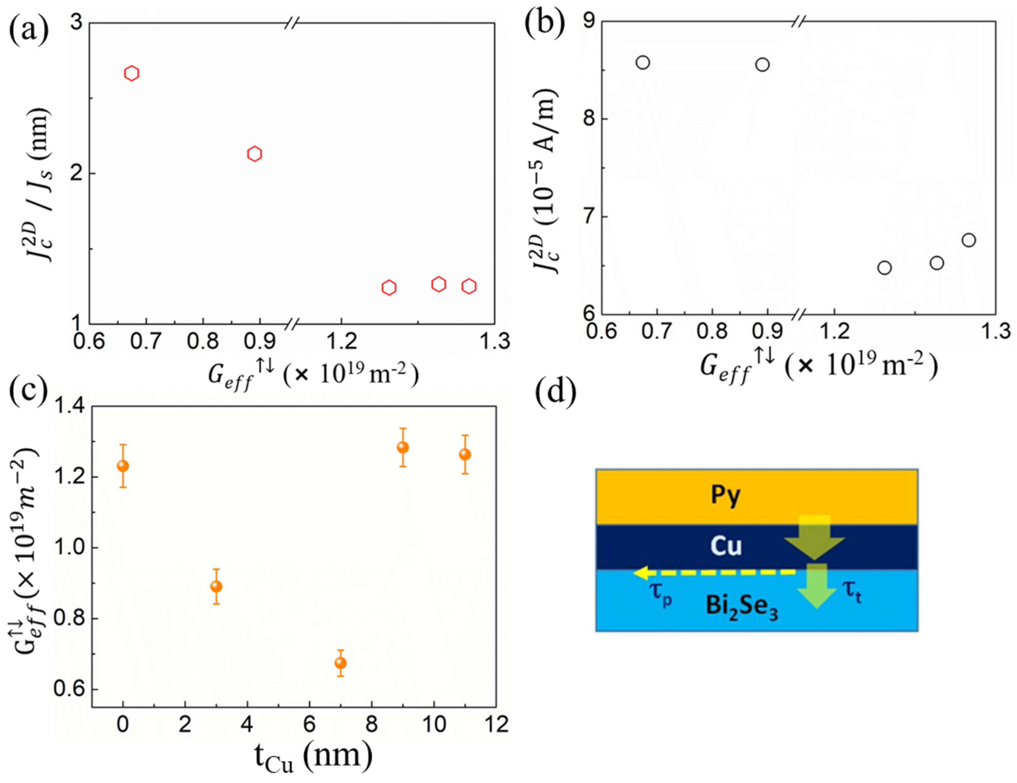
3. Results and Discussion
4. Conclusions
Supplementary Materials
Author Contributions
Funding
Data Availability Statement
Acknowledgments
Conflicts of Interest
References
- Han, W.; Otani, Y.; Maekawa, S. Quantum materials for spin and charge conversion. npj Quantum Mater. 2018, 3, 27. [Google Scholar] [CrossRef] [Green Version]
- Manchon, A.; Koo, H.C.; Nitta, J.; Frolov, S.M.; Duine, R.A. New perspectives for Rashba spin-orbit coupling. Nat. Mater. 2015, 14, 871–882. [Google Scholar] [CrossRef] [PubMed] [Green Version]
- Longo, E.; Belli, M.; Alia, M.; Rimoldi, M.; Cecchini, R.; Longo, M.; Wiemer, C.; Locatelli, L.; Tsipas, P.; Dimoulas, A.; et al. Large Spin-to-Charge Conversion at Room Temperature in Extended Epitaxial Sb2Te3 Topological Insulator Chemically Grown on Silicon. Adv. Funct. Mater. 2022, 32, 2109361. [Google Scholar] [CrossRef]
- Sun, R.; Yang, S.; Yang, X.; Vetter, E.; Sun, D.; Li, N.; Su, L.; Li, Y.; Li, Y.; Gong, Z.-Z.; et al. Large Tunable spin-to-charge conversion induced by hybrid Rashba and Dirac surface states in topological insulator heterostructures. Nano Lett. 2019, 19, 4420–4426. [Google Scholar] [CrossRef]
- Manipatruni, S.; Nikonov, D.E.; Young, I.A. Beyond CMOS computing with spin and polarization. Nat. Phys. 2018, 14, 338–343. [Google Scholar] [CrossRef]
- Manipatruni, S.; Nikonov, D.E.; Lin, C.-C.; Gosavi, T.A.; Liu, H.; Prasad, B.; Huang, Y.-L.; Bonturim, E.; Ramesh, R.; Young, I.A. Scalable energy-efficient magnetoelectric spin-orbit logic. Nature 2019, 565, 35–42. [Google Scholar] [CrossRef]
- Wang, H.; Kally, J.; Lee, J.S.; Liu, T.; Chang, H.; Hickey, D.R.; Mkhoyan, K.A.; Wu, M.; Richardella, A.; Samarth, N. Surface-state-dominated spin-charge current conversion in topological-insulator–ferromagnetic-insulator heterostructures. Phys. Rev. Lett. 2016, 117, 076601. [Google Scholar] [CrossRef] [Green Version]
- Rojas-Sánchez, J.-C.; Oyarzún, S.; Fu, Y.; Marty, A.; Vergnaud, C.; Gambarelli, S.; Vila, L.; Jamet, M.; Ohtsubo, Y.; Taleb-Ibrahimi, A.; et al. Spin-to-charge conversion at room temperature by spin pumping into a new type of topological insulator: α-Sn films. Highly efficient spin-to-charge conversion in a topological insulator is observed at room temperature. Phys. Rev. Lett. 2016, 116, 096602. [Google Scholar] [CrossRef] [Green Version]
- Noel, P.; Thomas, C.; Fu, Y.; Vila, L.; Haas, B.; Jouneau, P.-H.; Gambarelli, S.; Meunier, T.; Ballet, P.; Attane, J.P. Highly efficient spin-to-charge current conversion in strained HgTe surface states protected by a HgCdTe layer. Phys. Rev. Lett. 2018, 120, 167201. [Google Scholar] [CrossRef] [Green Version]
- DC, M.; Chen, J.Y.; Peterson, T.; Sahu, P.; Ma, B.; Mousavi, N.; Harjani, R.; Wang, J.P. Observation of high spin-to-charge conversion by sputtered bismuth selenide thin films at room temperature. Nano Lett. 2019, 19, 4836–4844. [Google Scholar] [CrossRef]
- Jamali, M.; Lee, J.S.; Jeong, J.S.; Mahfouzi, F.; Lv, Y.; Zhao, Z.; Nikolic, B.K.; Mkhoyan, K.A.; Samarth, N.; Wang, J.-P. Giant Spin pumping and inverse spin Hall effect in the presence of surface and bulk spin-orbit coupling of topological insulators Bi2Se3. Nano Lett. 2015, 15, 7126–7132. [Google Scholar] [CrossRef] [PubMed]
- Su, S.H.; Chuang, P.-Y.; Lee, J.-C.; Chong, C.-W.; Li, Y.W.; Lin, Z.M.; Chen, Y.-C.; Cheng, C.-M.; Huang, J.C.A. Spin-to-Charge Conversion Manipulated by Fine-Tuning the Fermi Level of Topological Insulator (Bi1–xSbx)2Te3. ACS Appl. Electron. Mater. 2021, 3, 2988–2994. [Google Scholar] [CrossRef]
- Du, C.; Wang, H.; Yang, F.; Chris Hammel, P. Enhancement of pure spin currents in spin pumping Y3Fe5O12/Cu/Metal trilayers through spin conductance matching. Phys. Rev. Appl. 2014, 1, 044004. [Google Scholar] [CrossRef] [Green Version]
- Zhang, W.; Jungfleisch, M.B.; Jiang, W.; Pearson, J.E.; Hoffmann, A. Spin pumping and inverse Rashba-Edelstein effect in NiFe/Ag/Bi and NiFe/Ag/Sb. J. Appl. Phys. 2015, 117, 17C727. [Google Scholar] [CrossRef]
- Tserkovnyak, Y.; Brataas, A.; Bauer, G.E.W. Spin pumping and magnetization dynamics in metallic multilayers. Phys. Rev. B 2002, 66, 224403. [Google Scholar] [CrossRef] [Green Version]
- Deorani, P.; Yanga, H. Role of spin mixing conductance in spin pumping: Enhancement of spin pumping efficiency in Ta/Cu/Py structures. Appl. Phys. Lett. 2013, 103, 232408. [Google Scholar] [CrossRef] [Green Version]
- Ding, J.; Zhang, W.; Jungfleisch, M.B.; Pearson, J.E.; Ohldag, H.; Novosad, V.; Hoffmann, A. Direct observation of spin accumulation in Cu induced by spin pumping. Phys. Rev. Res. 2020, 2, 013262. [Google Scholar] [CrossRef] [Green Version]
- Kondou, K.; Yoshimi, R.; Tsukazaki, A.; Fukuma, Y.; Matsuno, J.; Takahashi, K.S.; Kawasaki, M.; Tokura, Y.; Otani, Y. Fermi-level-dependent charge-to-spin current conversion by Dirac surface state of topological insulators. Nat. Phys. 2016, 12, 1027–1031. [Google Scholar] [CrossRef] [Green Version]
- Wray, L.A.; Xu, S.; Neupane, M.; Fedorov, A.V.; Hor, Y.S.; Cava, R.J.; Hasan, M.Z. Chemically gated electronic structure of a superconducting doped topological insulator system. J. Phys. Conf. Ser. 2013, 449, 012037. [Google Scholar] [CrossRef] [Green Version]
- Tsukahara, A.; Ando, Y.; Kitamura, Y.; Emoto, H.; Shikoh, E.; Delmo, M.P.; Shinjo, T.; Shiraishi, M. Self-induced inverse spin Hall effect in permalloy at room temperature. Phys. Rev. B 2014, 89, 235317. [Google Scholar] [CrossRef]
- Azevedo, A.; Vilela-Leão, L.H.; Rodríguez-Suárez, R.L.; Lacerda Santos, A.F.; Rezende, S.M. Spin pumping and anisotropic magnetoresistance voltages in magnetic bilayers: Theory and experiment. Phys. Rev. B 2011, 83, 144402. [Google Scholar] [CrossRef]
- Bai, L.; Hyde, P.; Gui, Y.S.; Hu, C.-M.; Vlaminck, V.; Pearson, J.E.; Bader, S.D.; Hoffmann, A. Universal Method for Separating Spin Pumping from Spin Rectification Voltage of Ferromagnetic Resonance. Phys. Rev. Lett. 2013, 111, 217602. [Google Scholar] [CrossRef] [PubMed]
- Bai, L.; Feng, Z.; Hyde, P.; Ding, H.F.; Hu, C.-M. Distinguishing spin pumping from spin rectification in a Pt/Py bilayer through angle dependent line shape analysis. Appl. Phys. Lett. 2013, 102, 242402. [Google Scholar]
- Zhang, W.; Peng, B.; Han, F.; Wang, Q.; Soh, W.T.; Ong, C.K.; Zhang, W. Separating inverse spin Hall voltage and spin rectification voltage by inverting spin injection direction. Appl. Phys. Lett. 2016, 108, 102405. [Google Scholar] [CrossRef] [Green Version]
- Mendes, J.B.S.; Gamino, M.; Cunha, R.O.; Abrão, J.E.; Rezende, S.M.; Azevedo, A. Unveiling the spin-to-charge current conversion signal in the topological insulator Bi2Se3 by means of spin pumping experiments. Phys. Rev. Mater. 2021, 5, 024206. [Google Scholar] [CrossRef]
- Singh, B.B.; Jena, S.K.; Samanta, M.; Biswas, K.; Bedanta, S. High Spin to Charge Conversion Efficiency in Electron Beam-Evaporated Topological Insulator Bi2Se3. ACS Appl. Mater. Interfaces 2020, 12, 53409–53415. [Google Scholar] [CrossRef]
- Ni, L.; Chen, Z.; Lu, X.; Yan, Y.; Jin, L.; Zhou, J.; Yue, W.; Zhang, Z.; Zhang, L.; Wang, W.; et al. Strong interface-induced spin-charge conversion in YIG/Cr heterostructures. Appl. Phys. Lett. 2020, 117, 112402. [Google Scholar] [CrossRef]
- Tao, X.; Liu, Q.; Miao, B.; Yu, R.; Feng, Z.; Sun, L.; You, B.; Du, J.; Chen, K.; Zhang, S.; et al. Self-consistent determination of spin Hall angle and spin diffusion length in Pt and Pd: The role of the interface spin loss. Sci. Adv. 2018, 4, 1670. [Google Scholar] [CrossRef] [Green Version]
- Chen, K.; Zhang, S. Spin Pumping Induced Electric Voltage. IEEE Magn. Lett. 2015, 6, 1. [Google Scholar] [CrossRef]
- Gannett, W.; Kellera, M.W.; Nembach, H.T.; Silva, T.J.; Chiaramonti, A.N. Suppression of spin pumping between Ni80Fe20 and Cu by a graphene interlayer. J. Appl. Phys. 2015, 117, 213907. [Google Scholar] [CrossRef] [Green Version]
- Zhang, S.; Fert, A. Conversion between spin and charge currents with topological insulators. Phys. Rev. B 2016, 94, 184423. [Google Scholar] [CrossRef]
- Gonçalves, A.M.; Garcia, F.; Lee, H.K.; Smith, A.; Soledade, P.R.; Passos, C.A.C.; Costa, M.; Souza-Neto, N.M.; Krivorotov, I.N.; Sampaio, L.C.; et al. Oscillatory interlayer coupling in spin Hall systems. Sci. Rep. 2018, 8, 2318. [Google Scholar] [CrossRef] [PubMed] [Green Version]
- Montoya, E.; Heinrich, B.; Girt, E. Quantum Well State Induced Oscillation of Pure Spin Currents in Fe/Au/Pd (001) Systems. Phys. Rev. Lett. 2014, 113, 136601. [Google Scholar] [CrossRef]
- Dey, R.; Prasad, N.; Register, L.F.; Banerjee, S.K. Conversion of spin current into charge current in a topological insulator: Role of the interface. Phys. Rev. B 2018, 97, 174406. [Google Scholar] [CrossRef] [Green Version]
- Kim, J.; Chen, Y.-T.; Karube, S.; Takahashi, S.; Kondou, K.; Tatara, G.; Otani, Y. Evaluation of bulk-interface contributions to Edelstein magnetoresistance at metal/oxide interfaces. Phys. Rev. B 2017, 96, 140409. [Google Scholar] [CrossRef] [Green Version]
- Su, S.H.; Chuang, P.-Y.; Chen, S.W.; Chen, H.Y.; Tung, Y.; Chen, W.-C.; Wang, C.-H.; Yang, Y.-W.; Huang, J.C.A.; Chang, T.-R.; et al. Selective Hydrogen etching leads to 2D Bi(111) bilayers on Bi2Se3: Large Rashba splitting in topological insulator heterostructure. Chem. Mater. 2017, 29, 8992–9000. [Google Scholar] [CrossRef]
- Rojas Sánchez, J.C.; Vila, L.; Desfonds, G.; Gambarelli, S.; Attané, J.P.; De Teresa, J.M.; Magén, C.; Fert, A. Spin-to-charge conversion using Rashba coupling at the interface between non-magnetic materials. Nat. Commun. 2013, 4, 2944. [Google Scholar] [CrossRef] [Green Version]
- Zhou, C.; Liu, Y.P.; Wang, Z.; Ma, S.J.; Jia, M.W.; Wu, R.Q.; Zhou, L.; Zhang, W.; Liu, M.K.; Wu, Y.Z.; et al. Broadband Terahertz Generation via the Interface Inverse Rashba-Edelstein Effect. Phys. Rev. Lett. 2018, 121, 086801. [Google Scholar] [CrossRef] [Green Version]
- Wang, X.; Cheng, L.; Zhu, D.; Wu, Y.; Chen, M.; Wang, Y.; Zhao, D.; Boothroyd, C.B.; Lam, Y.M.; Zhu, J.X.; et al. Ultrafast Spin-to-Charge Conversion at the Surface of Topological Insulator Thin Films. Adv. Mater. 2018, 30, 1802356. [Google Scholar] [CrossRef] [Green Version]
- Cheng, P.; Song, C.; Zhang, T.; Zhang, Y.; Wang, Y.; Jia, J.-F.; Wang, J.; Wang, Y.; Zhu, B.-F.; Chen, X.; et al. Landau Quantization of Topological Surface States in Bi2Se3. Phys. Rev. Lett. 2010, 105, 076801. [Google Scholar] [CrossRef] [Green Version]
- Atuchin, V.V.; Golyashov, V.A.; Kokh, K.A.; Korolkov, I.V.; Kozhukhov, A.S.; Kruchinin, V.N.; Makarenko, S.V.; Pokrovsky, L.D.; Prosvirin, I.P.; Romanyuk, K.N.; et al. Formation of Inert Bi2Se3(0001) Cleaved Surface. Cryst. Growth Des. 2011, 11, 5507–5514. [Google Scholar] [CrossRef]


Publisher’s Note: MDPI stays neutral with regard to jurisdictional claims in published maps and institutional affiliations. |
© 2022 by the authors. Licensee MDPI, Basel, Switzerland. This article is an open access article distributed under the terms and conditions of the Creative Commons Attribution (CC BY) license (https://creativecommons.org/licenses/by/4.0/).
Share and Cite
Su, S.H.; Chong, C.-W.; Lee, J.-C.; Chen, Y.-C.; Marchenkov, V.V.; Huang, J.-C.A. Effect of Cu Intercalation Layer on the Enhancement of Spin-to-Charge Conversion in Py/Cu/Bi2Se3. Nanomaterials 2022, 12, 3687. https://doi.org/10.3390/nano12203687
Su SH, Chong C-W, Lee J-C, Chen Y-C, Marchenkov VV, Huang J-CA. Effect of Cu Intercalation Layer on the Enhancement of Spin-to-Charge Conversion in Py/Cu/Bi2Se3. Nanomaterials. 2022; 12(20):3687. https://doi.org/10.3390/nano12203687
Chicago/Turabian StyleSu, Shu Hsuan, Cheong-Wei Chong, Jung-Chuan Lee, Yi-Chun Chen, Vyacheslav Viktorovich Marchenkov, and Jung-Chun Andrew Huang. 2022. "Effect of Cu Intercalation Layer on the Enhancement of Spin-to-Charge Conversion in Py/Cu/Bi2Se3" Nanomaterials 12, no. 20: 3687. https://doi.org/10.3390/nano12203687