
Investigation of Combinatorial WO3-MoO3 Mixed Layers by Spectroscopic Ellipsometry Using Different Optical Models

 , , and
Abstract
:1. Introduction
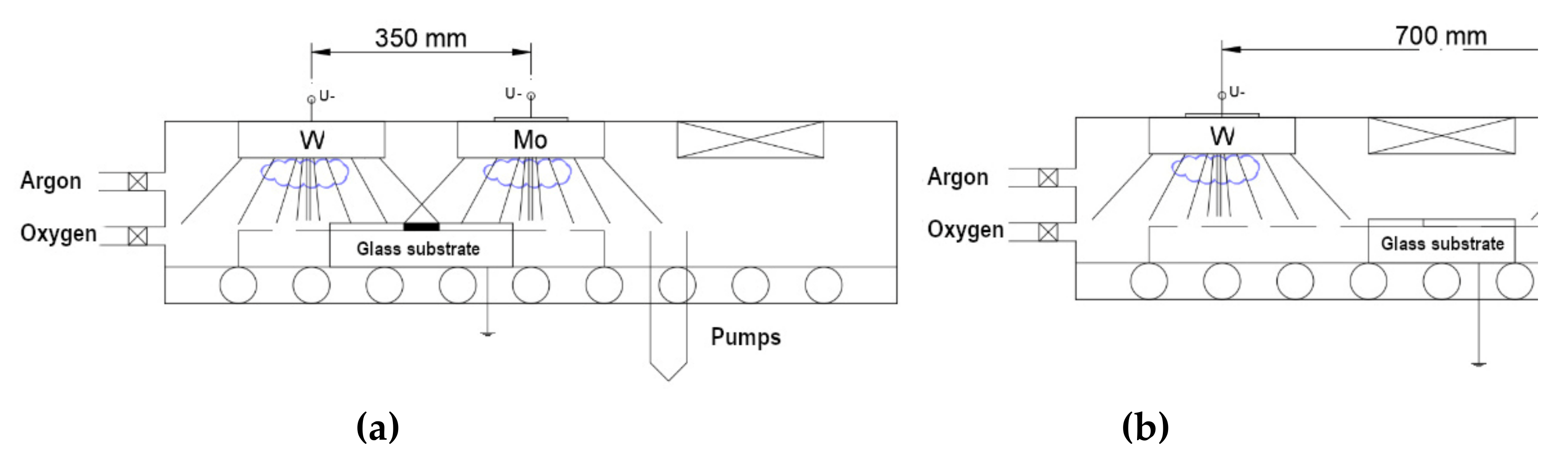
2. Materials and Methods
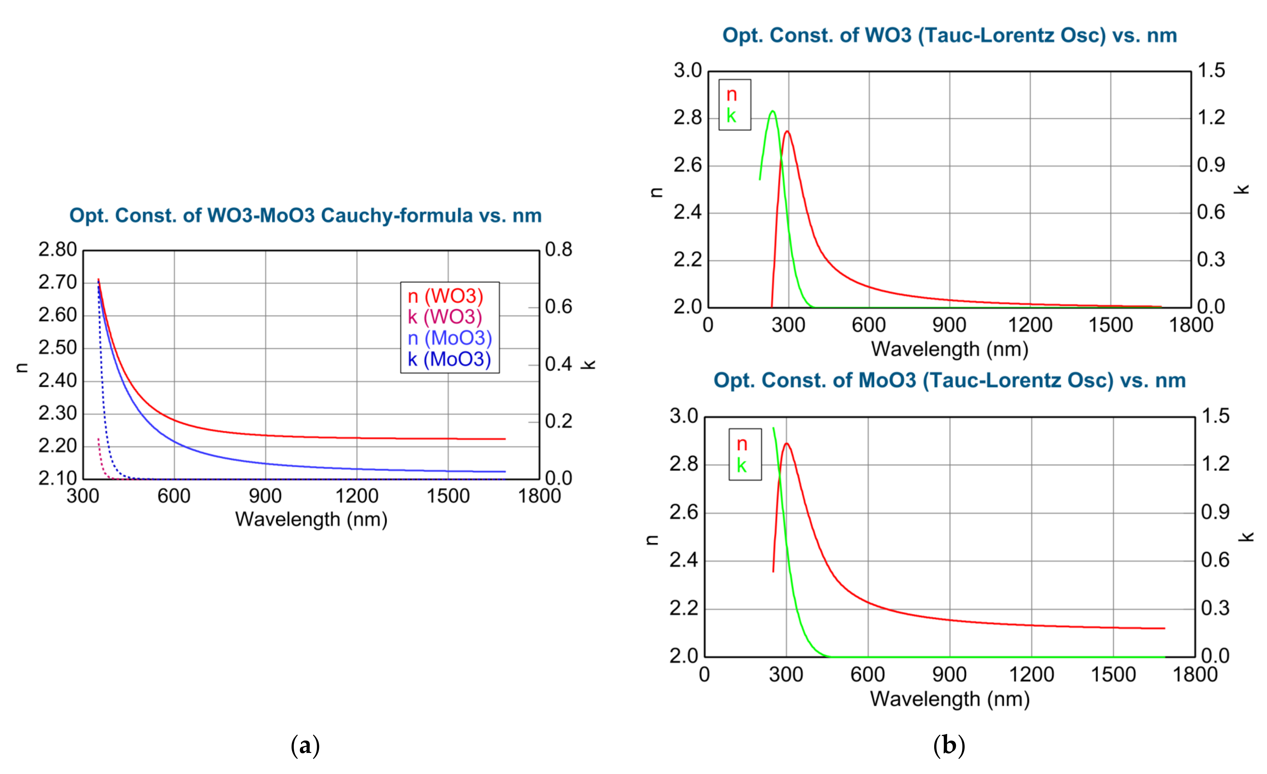
Dispersion Relations
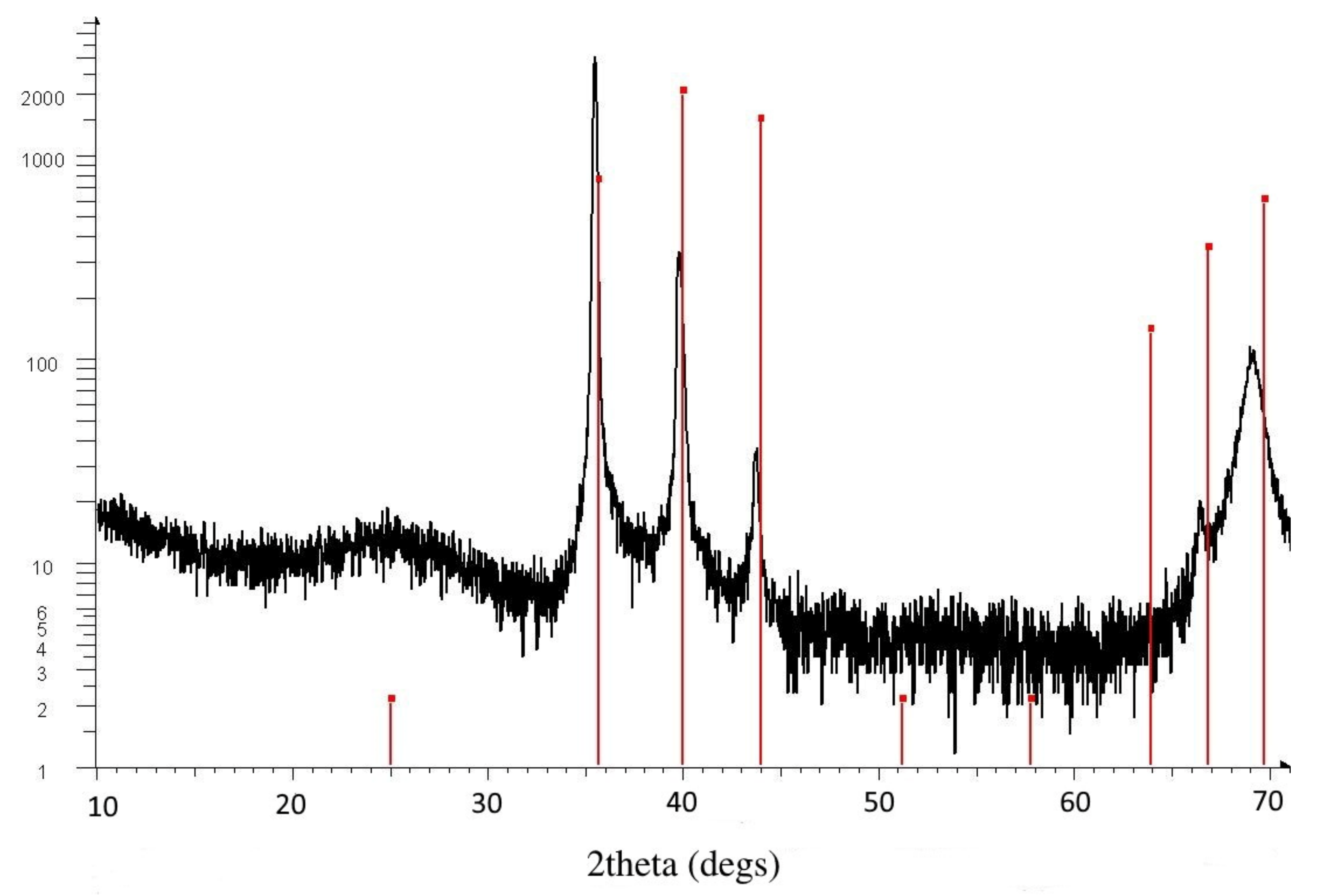
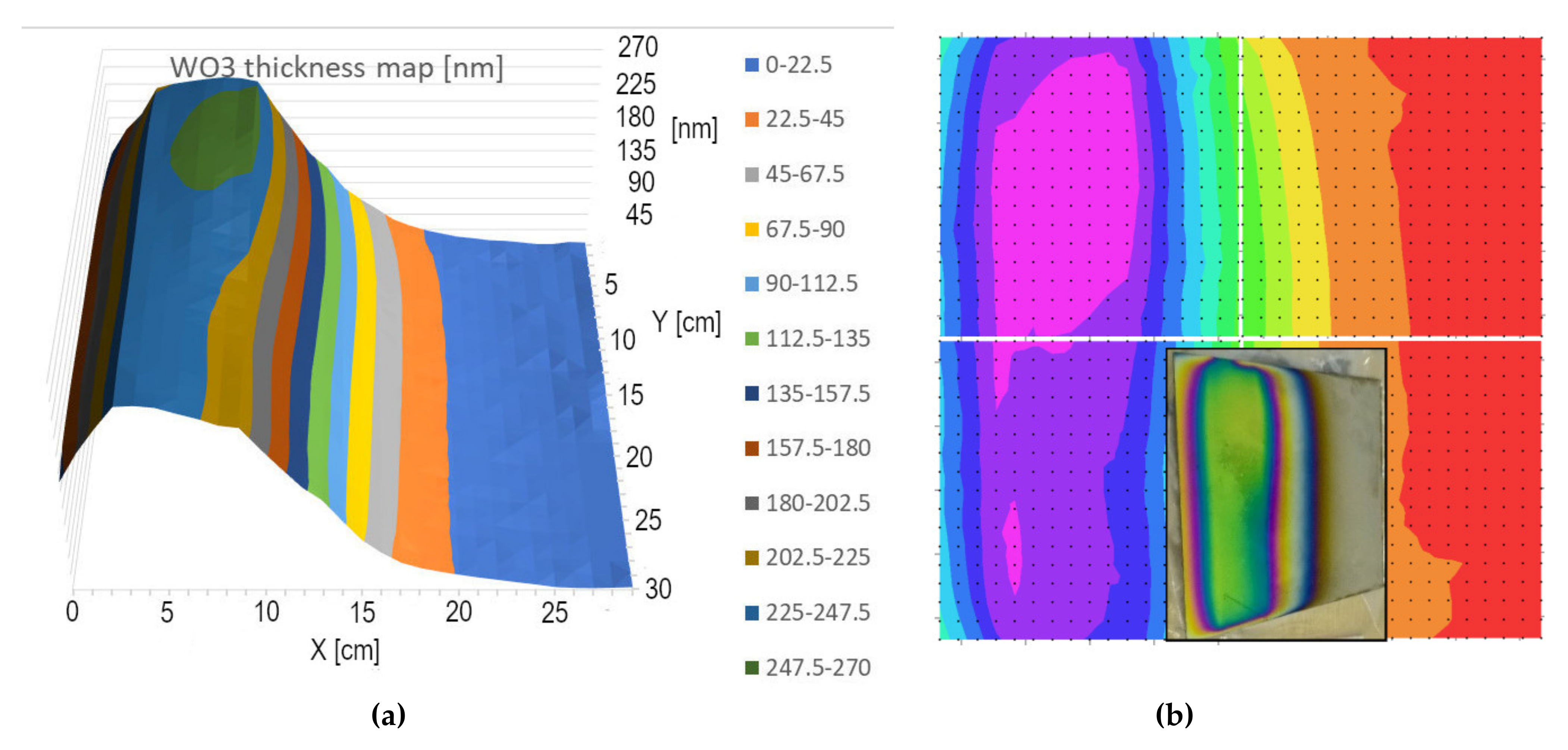
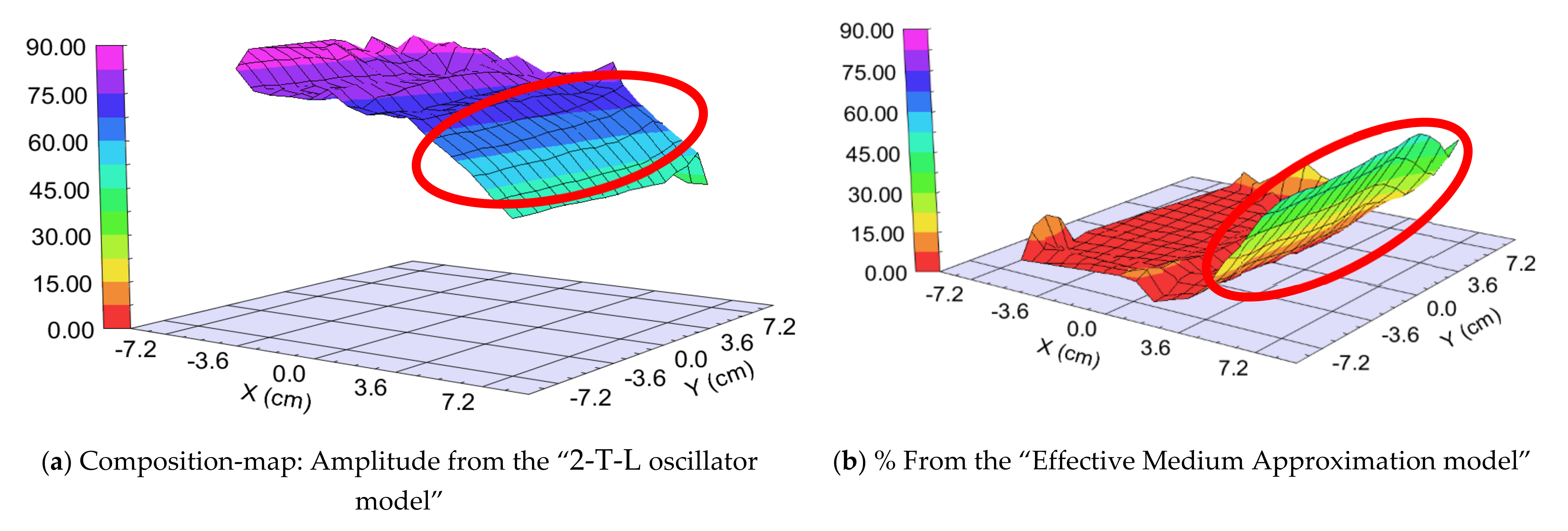
3. Results and Discussion
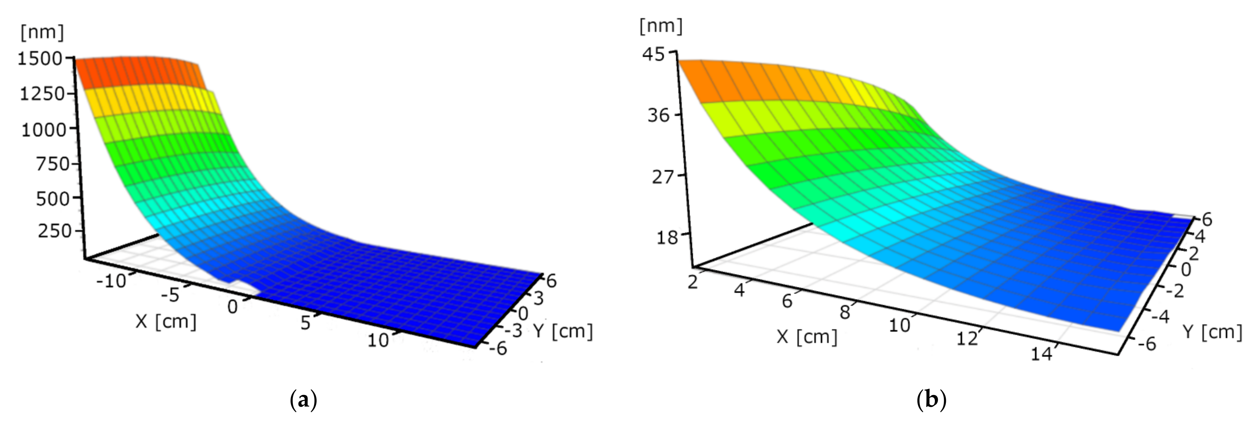
3.1. Single-Target Samples
3.2. Thickness vs. Power
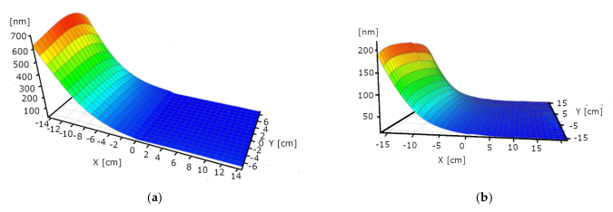
3.3. Double-Target Samples
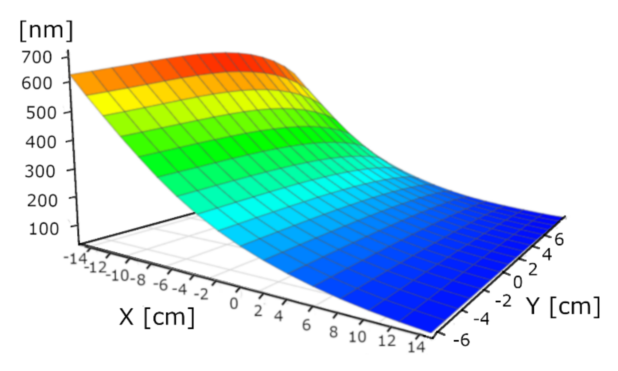
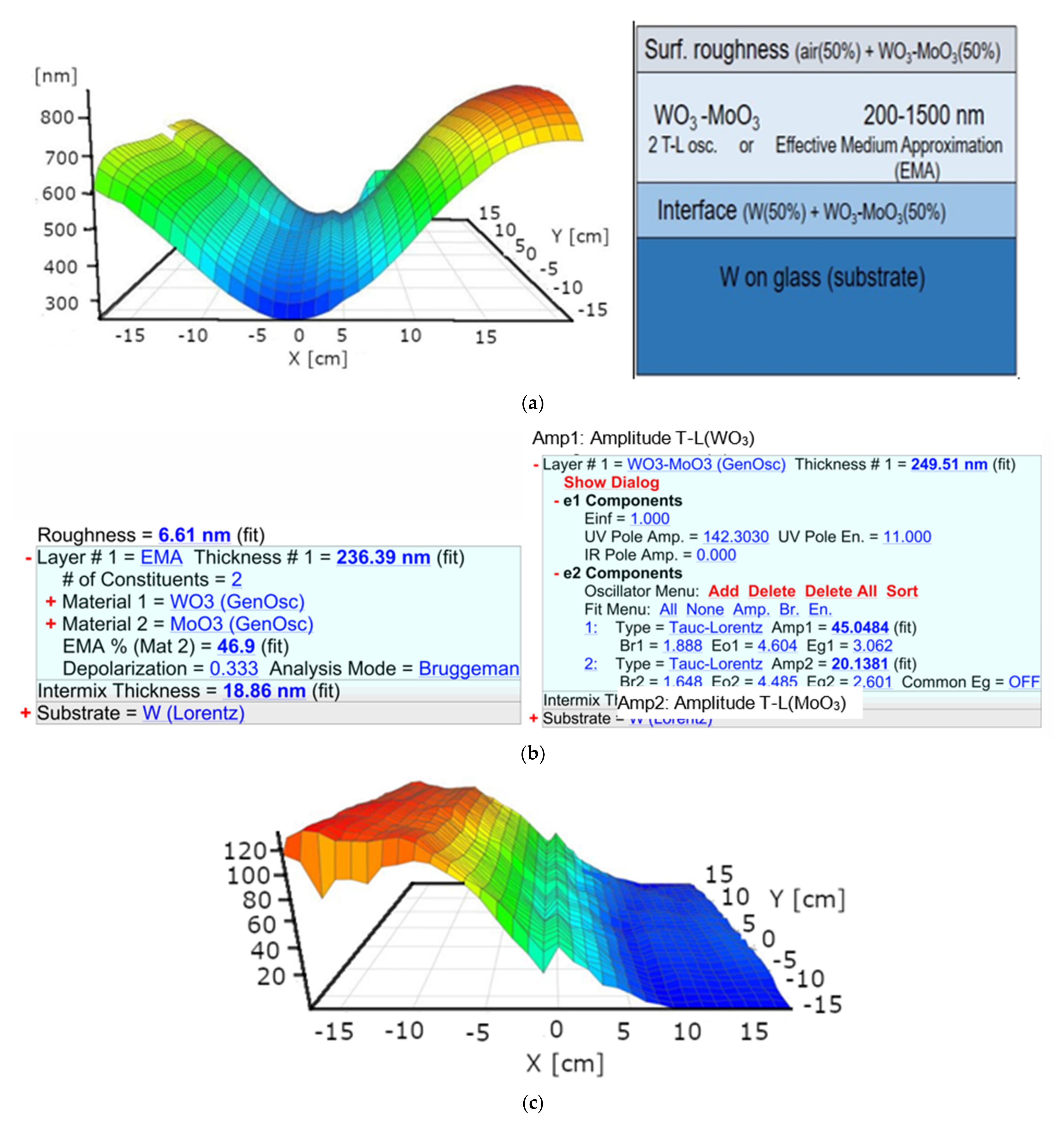
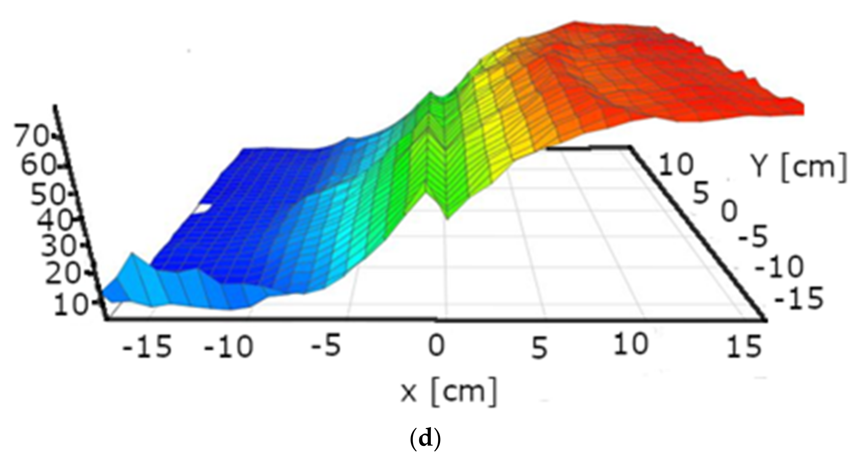
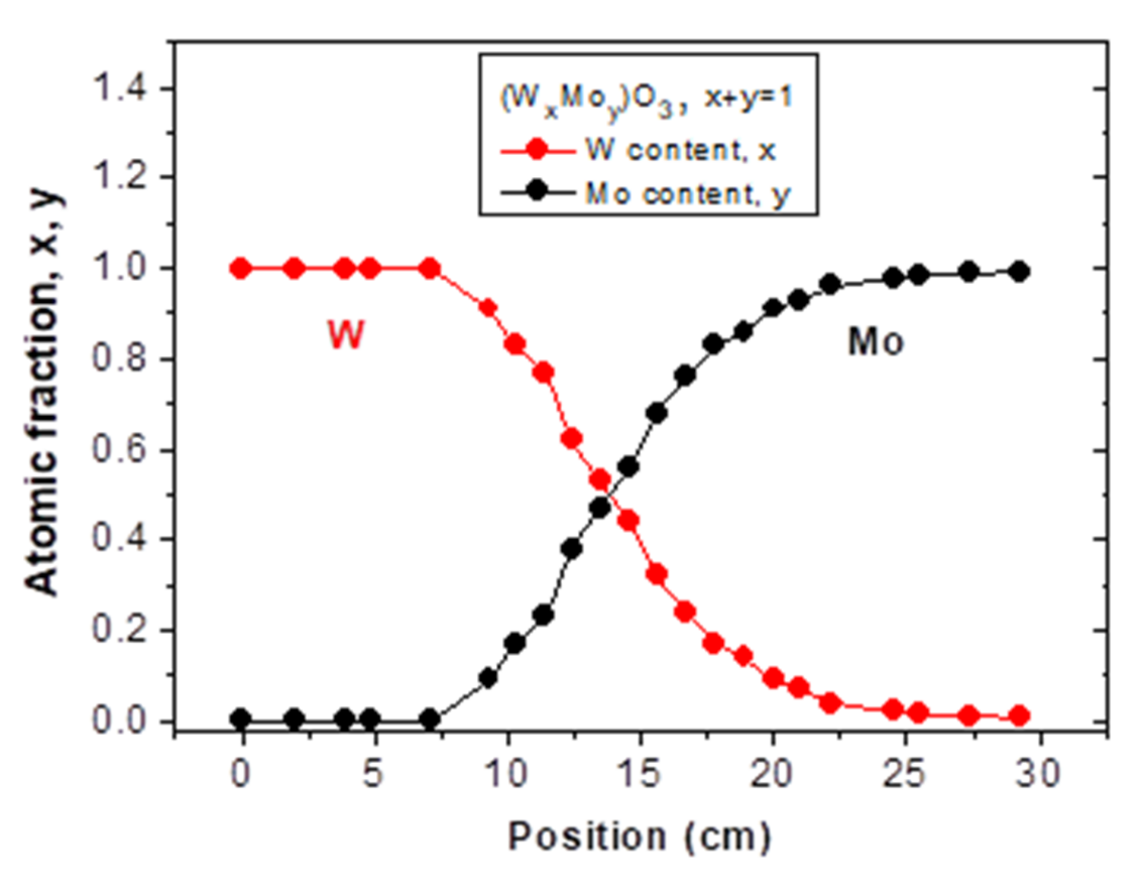
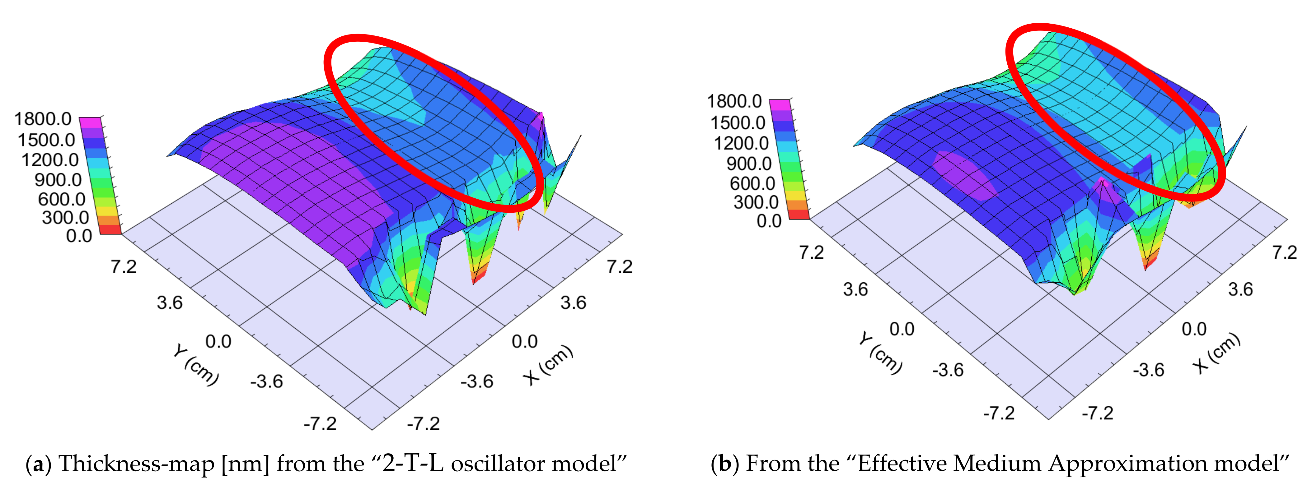
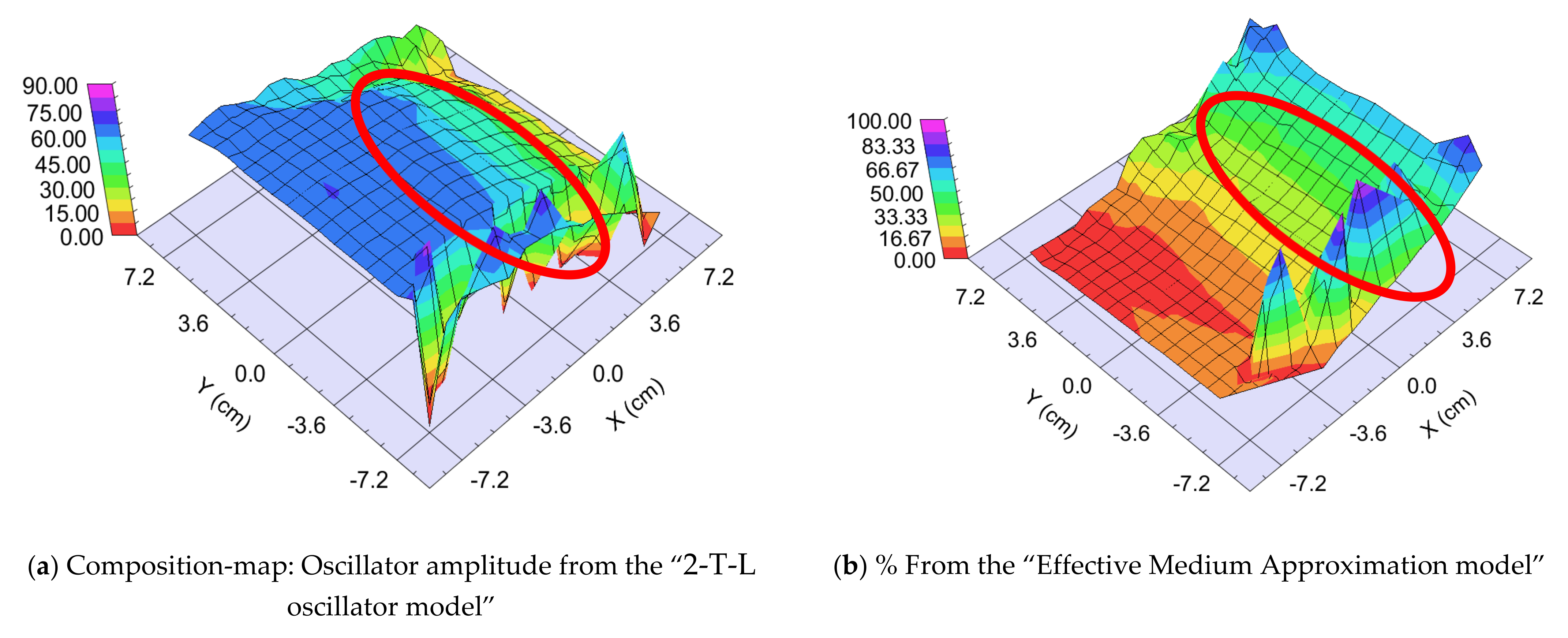
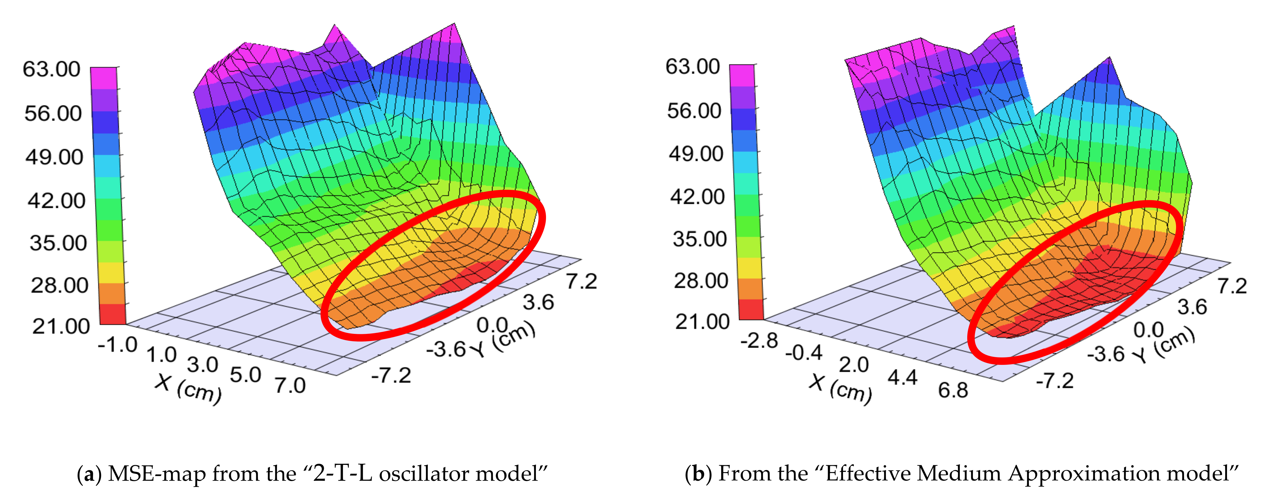
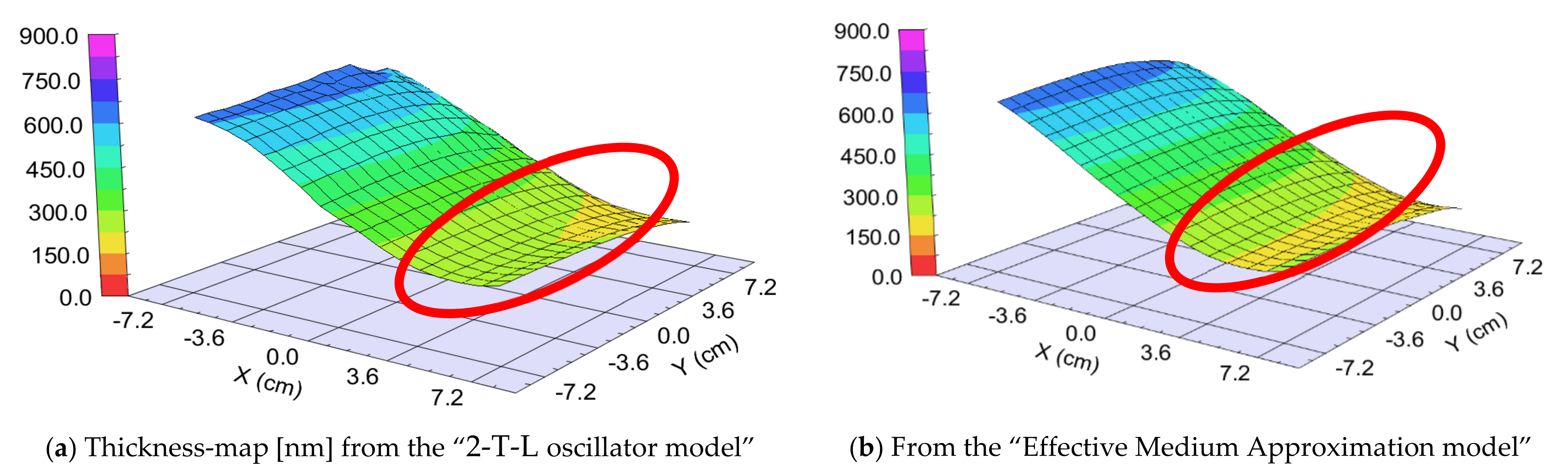
3.3.1. Targets in Closer Position
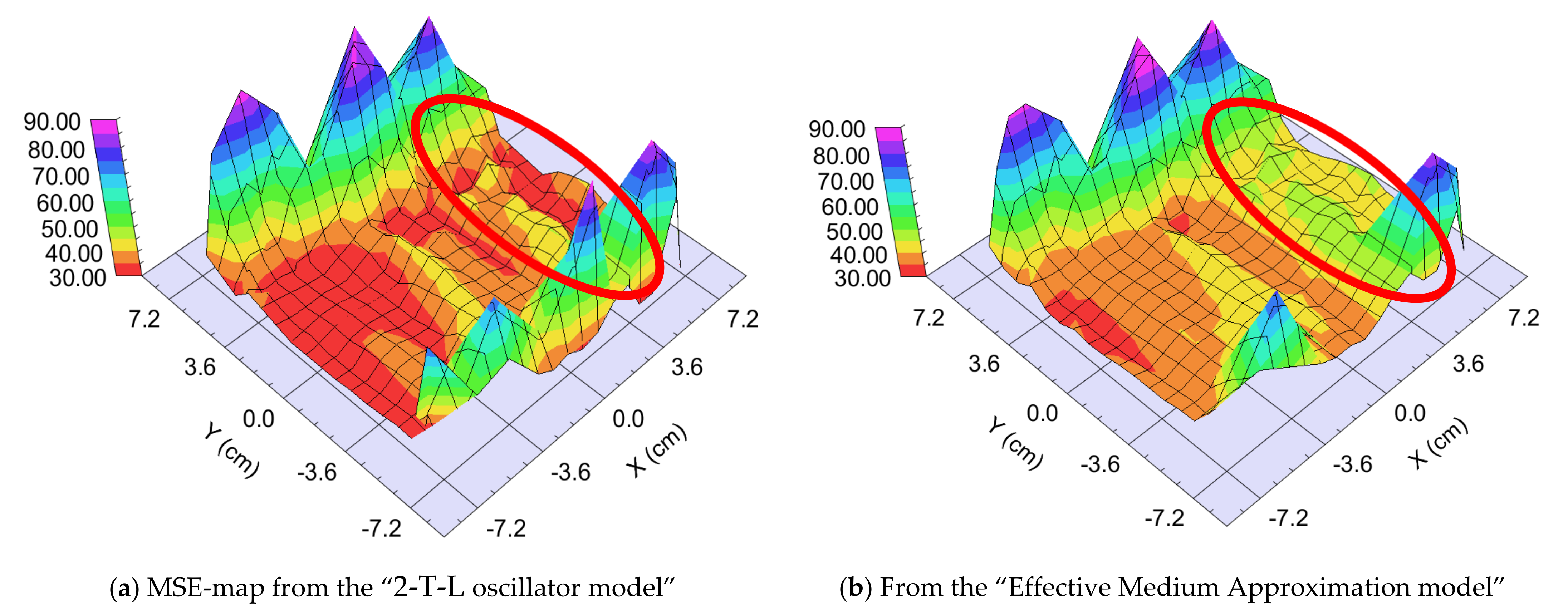
3.3.2. Atomic (or “Molecular”) Mixture vs. “Superlattice”
“Fast” Sample, 25 cm/s Walking: ~0.5 nm “Sublayer Thickness”
“Slow” Sample, 1 cm/s Walking: 3–5 nm Sublayer Thickness
4. Conclusions
Author Contributions
Funding
Institutional Review Board Statement
Informed Consent Statement
Data Availability Statement
Conflicts of Interest
References
- Granqvist, C.G. Handbook of Inorganic Electrochromic Materials; Elsevier: Amsterdam, The Netherlands, 1995. [Google Scholar]
- Livage, J.; Ganguli, D. Sol-gel electrochromic coatings and devices: A review. Sol. Energy Mater. Sol. Cells. 2001, 68, 365–381. [Google Scholar] [CrossRef]
- Hsu, C.S.; Chan, C.C.; Huang, H.T.; Peng, C.H.; Hsu, W.C. Electrochromic properties of nanocrystalline MoO3 thin films. Thin Solid Film. 2008, 516, 4839–4844. [Google Scholar] [CrossRef]
- Lin, S.-Y.; Wang, C.-M.; Kao, K.-S.; Chen, Y.-C.; Liu, C.-C. Electrochromic properties of MoO3 thin films derived by a sol–gel process. J. Sol Gel Sci. Technol. 2010, 53, 51–58. [Google Scholar] [CrossRef]
- Madhavi, V.; Jeevan Kumar, P.; Kondaiah, P.; Hussain, O.M.; Uthanna, S. Effect of molybdenum doping on the electrochromic properties of tungsten oxide thin films by RF magnetron sputtering. Ionics 2014, 20, 1737–1745. [Google Scholar] [CrossRef]
- Ivanova, T.; Gesheva, K.A.; Kalitzova, M.; Hamelmann, F.; Luekermann, F.; Heinzmann, U. Electrochromic mixed films based on WO3 and MoO3, obtained by an APCVD method. J. Optoelectron. Adv. Mater. 2009, 11, 1513–1516. [Google Scholar]
- Novinrooz, A.; Sharbatdaran, M.; Noorkojouri, H. Structural and optical properties of WO3 electrochromic layers prepared by the sol-gel method. Cent. Eur. Sci. J. 2005, 3, 456–466. [Google Scholar] [CrossRef]
- Prameelaand, C.; Srinivasarao, K. Characterization of (MoO3)x-(Wo3)1-x composites. Int. J. Appl. Eng. Res. 2015, 10, 9865–9875. [Google Scholar]
- Zimmer, A.; Gilliot, M.; Broch, L.; Boulanger, C.; Stein, N.; Horwat, D. Morphological and chemical dynamics upon electrochemical cyclic sodiation of electrochromic tungsten oxide coatings extracted by in situ ellipsometry. Appl. Opt. 2020, 59, 3766–3772. [Google Scholar] [CrossRef] [PubMed]
- Sauvet, K.; Rougier, A.; Sauques, L. Electrochromic WO3 thin films active in the IR region. Sol. Energy Mater. Sol. Cells 2008, 92, 209–215. [Google Scholar] [CrossRef]
- Hales, J.S.; DeVries, M.; Dworak, B.; Woollam, J.A. Visible and infrared optical constants of electrochromic materials for emissivity modulation applications. Thin Solid Film. 1998, 313–314, 205. [Google Scholar] [CrossRef]
- Available online: https://www.jawoollam.com/products/m-2000-ellipsometer (accessed on 15 May 2022).
- Fried, M. On-line monitoring of solar cell module production by ellipsometry technique. Thin Solid Film. 2014, 571, 345–355. [Google Scholar] [CrossRef] [Green Version]
- Major, C.; Juhasz, G.; Labadi, Z.; Fried, M. High speed spectroscopic ellipsometry technique for on-line monitoring in large area thin layer production. In Proceedings of the IEEE 42nd Photovoltaic Specialist Conference, PVSC, New Orleans, LA, USA, 14–19 June 2015; pp. 1–6. Available online: https://ieeexplore.ieee.org/document/7355640 (accessed on 15 May 2022). [CrossRef]
- Horváth, Z.G.; Juhász, G.; Fried, M.; Major, C.; Petrik, P. Imaging Optical Inspection Device with a Pinhole Camera U.S. Patent 8437002 B2, 23 May 2007.
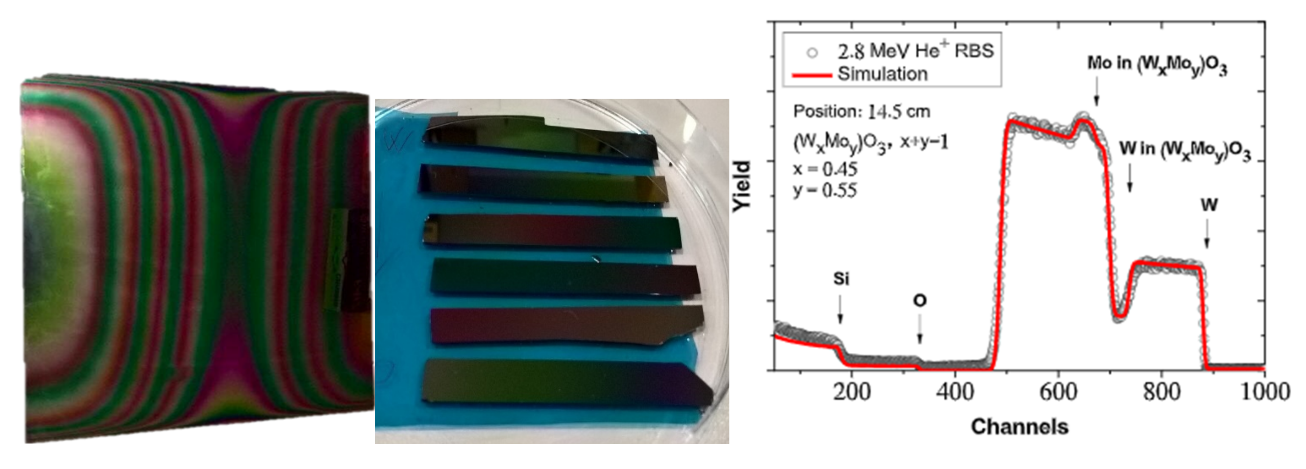
- Kótai, E. Computer Methods for Analysis and Simulation of RBS and ERDA spectra. Nucl. Instr. Meth. B 1994, 85, 588–596. [Google Scholar] [CrossRef]
- Bruggeman, D.A.G. Dielectric constant and conductivity of mixtures of isotropic materials. Ann. Phys. 1935, 24, 636–664. [Google Scholar] [CrossRef]
- Jellison, G.E., Jr.; Modine, F.A. Parameterization of the optical functions of amorphous materials in the interband region. Appl. Phys. Lett. 1996, 69, 371. [Google Scholar] [CrossRef]
- Petrik, P.; Fried, M. Mapping and imaging of thin films on large surfaces. Phys. Status Solidi 2022, 219, 2100800. [Google Scholar] [CrossRef]
- Labadi, Z.; Takács, D.; Zolnai, Z.; Petrik, P.; Fried, M. Electrochromic properties of mixed-oxide WO3/MoO3 films deposited by reactive sputtering. Appl. Surf. Sci. 2022; submitted. [Google Scholar]


| Sample Name | Target (s) | Target Position | Plasma Powers [kW] | Walking Cycles | Walking Speed |
|---|---|---|---|---|---|
| W-target-only | W | center | 0.75 | 500 | 5 cm/s |
| W-target-only | W | center | 1 | 500 | 5 cm/s |
| W-target-only | W | center | 1.5 | 500 | 5 cm/s |
| Mo-target-only | Mo | center | 0.75 | 500 | 5 cm/s |
| Mo-target-only | Mo | center | 1 | 500 | 5 cm/s |
| Mo-target-only | Mo | center | 1.5 | 500 | 5 cm/s |
| Double-target in closer position | W-Mo | Left-center | 0.75–1.5 | 300 | 5 cm/s |
| Double-target in distant position “Slow” | W-Mo | Left-right | 0.75–1.5 | 75 | 1 cm/s |
| Double-target in distant position “Fast” | W-Mo | Left-right | 0.75–1.5 | 1500 | 25 cm/s |
Publisher’s Note: MDPI stays neutral with regard to jurisdictional claims in published maps and institutional affiliations. |
© 2022 by the authors. Licensee MDPI, Basel, Switzerland. This article is an open access article distributed under the terms and conditions of the Creative Commons Attribution (CC BY) license (https://creativecommons.org/licenses/by/4.0/).
Share and Cite
Fried, M.; Bogar, R.; Takacs, D.; Labadi, Z.; Horvath, Z.E.; Zolnai, Z. Investigation of Combinatorial WO3-MoO3 Mixed Layers by Spectroscopic Ellipsometry Using Different Optical Models. Nanomaterials 2022, 12, 2421. https://doi.org/10.3390/nano12142421
Fried M, Bogar R, Takacs D, Labadi Z, Horvath ZE, Zolnai Z. Investigation of Combinatorial WO3-MoO3 Mixed Layers by Spectroscopic Ellipsometry Using Different Optical Models. Nanomaterials. 2022; 12(14):2421. https://doi.org/10.3390/nano12142421
Chicago/Turabian StyleFried, Miklos, Renato Bogar, Daniel Takacs, Zoltan Labadi, Zsolt Endre Horvath, and Zsolt Zolnai. 2022. "Investigation of Combinatorial WO3-MoO3 Mixed Layers by Spectroscopic Ellipsometry Using Different Optical Models" Nanomaterials 12, no. 14: 2421. https://doi.org/10.3390/nano12142421