
General Molecular Dynamics Approach to Understand the Mechanical Anisotropy of Monocrystalline Silicon under the Nanoscale Effects of Point Defect


Abstract
:1. Introduction
2. Model and Method
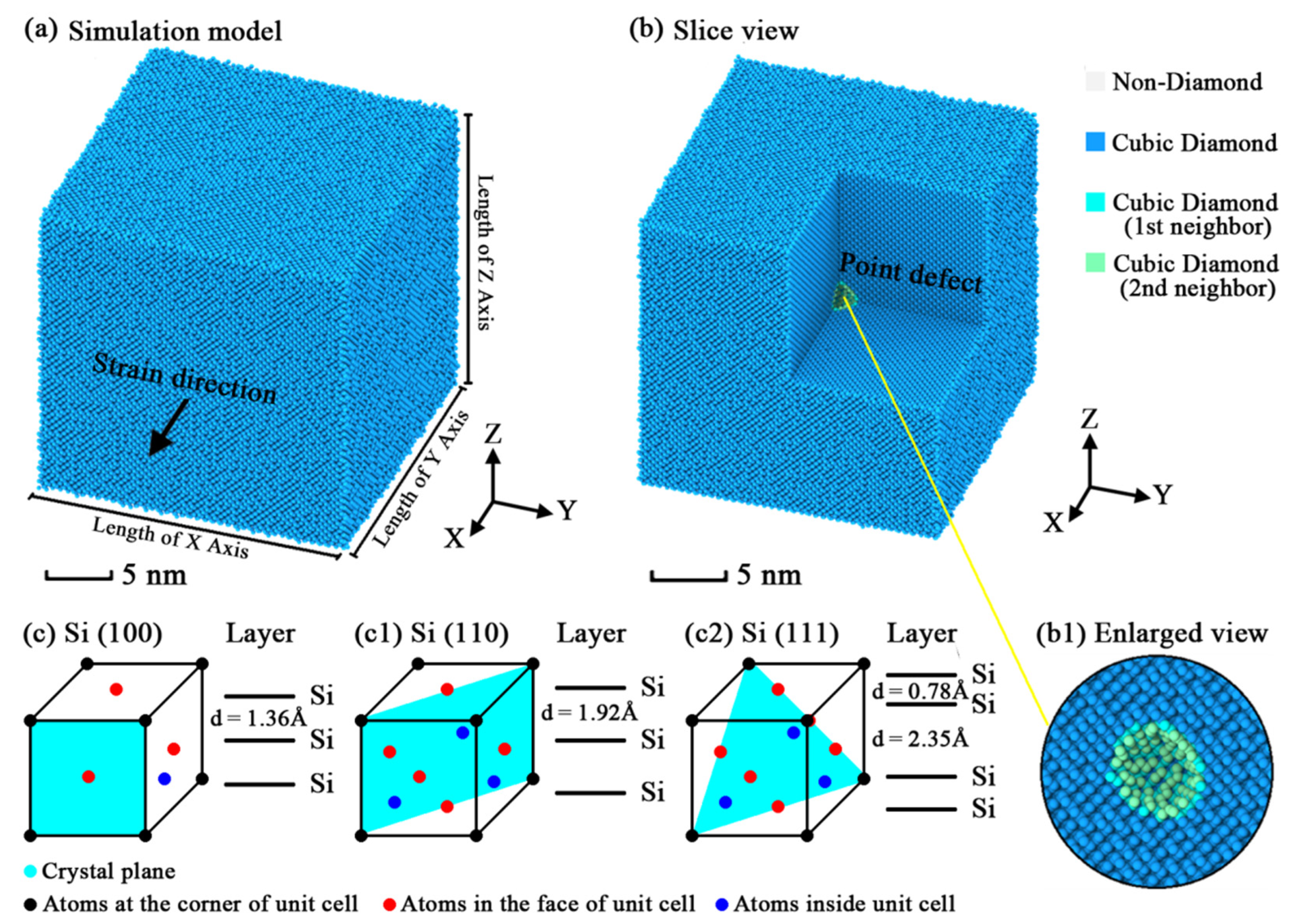
2.1. Model
2.2. Potential
2.3. Method
3. Results
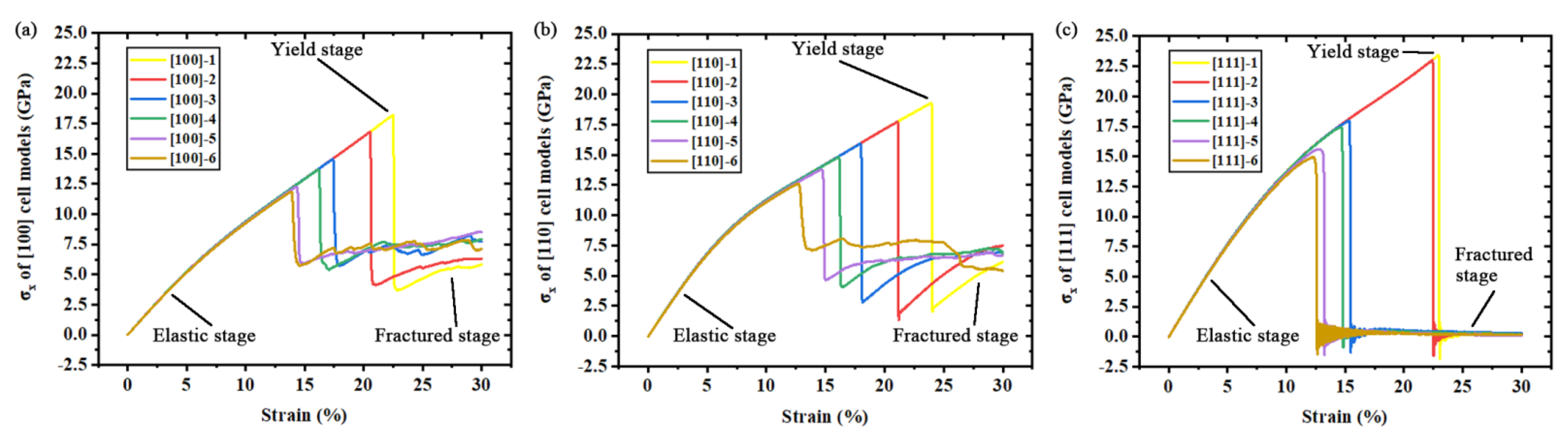
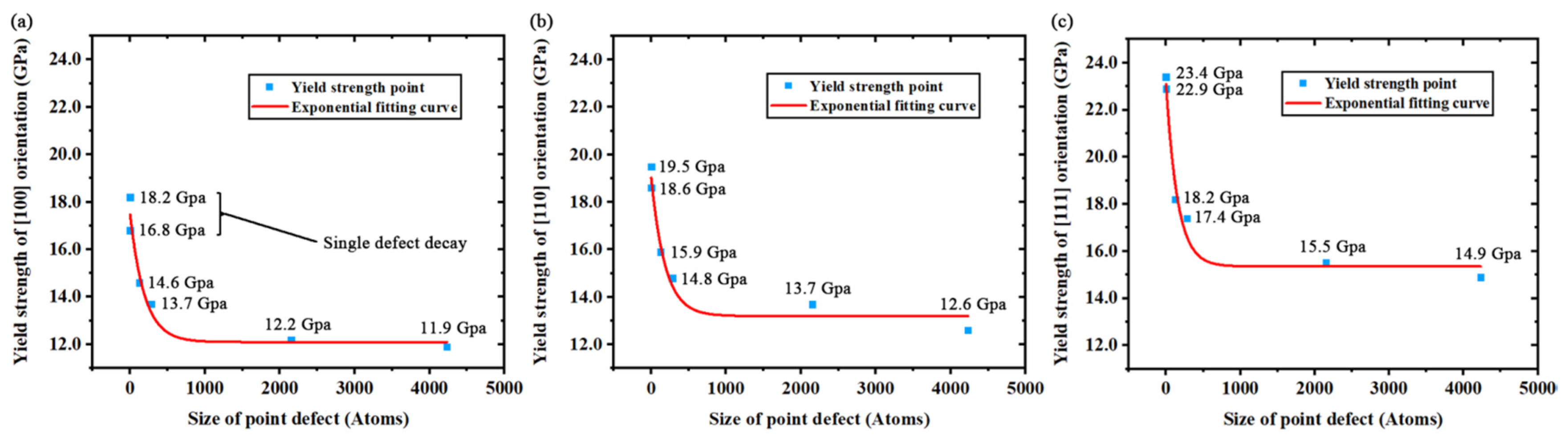
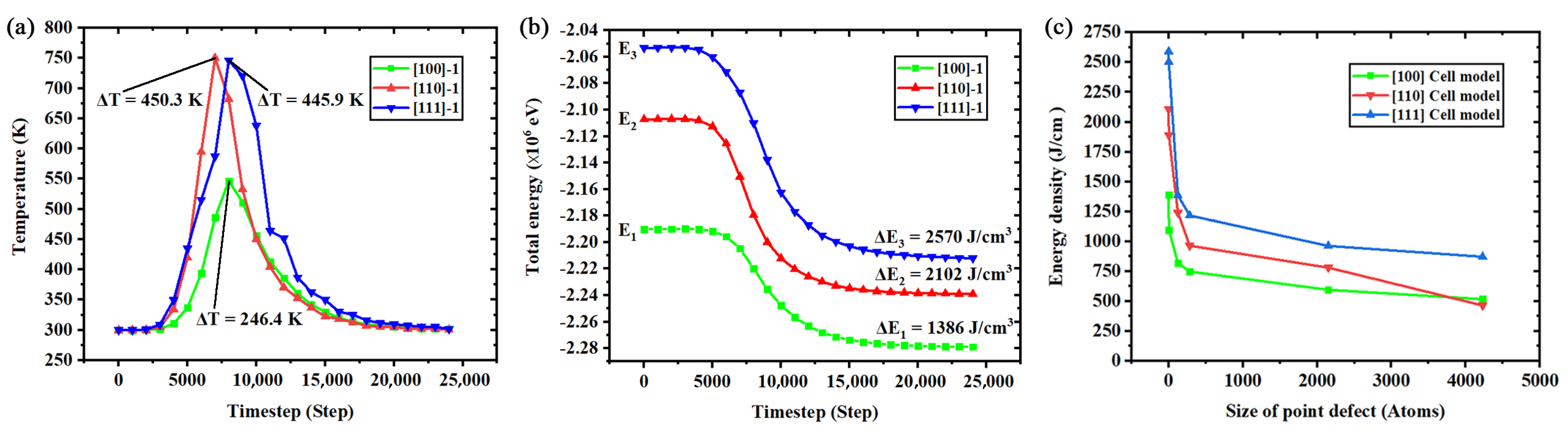
3.1. Anisotropy of Mechanical Performances
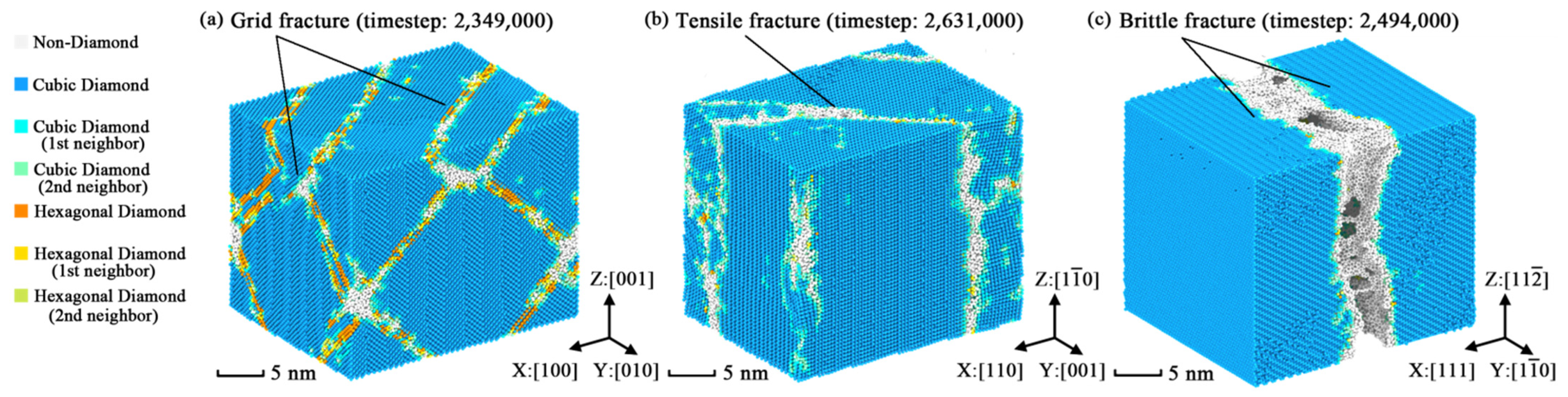
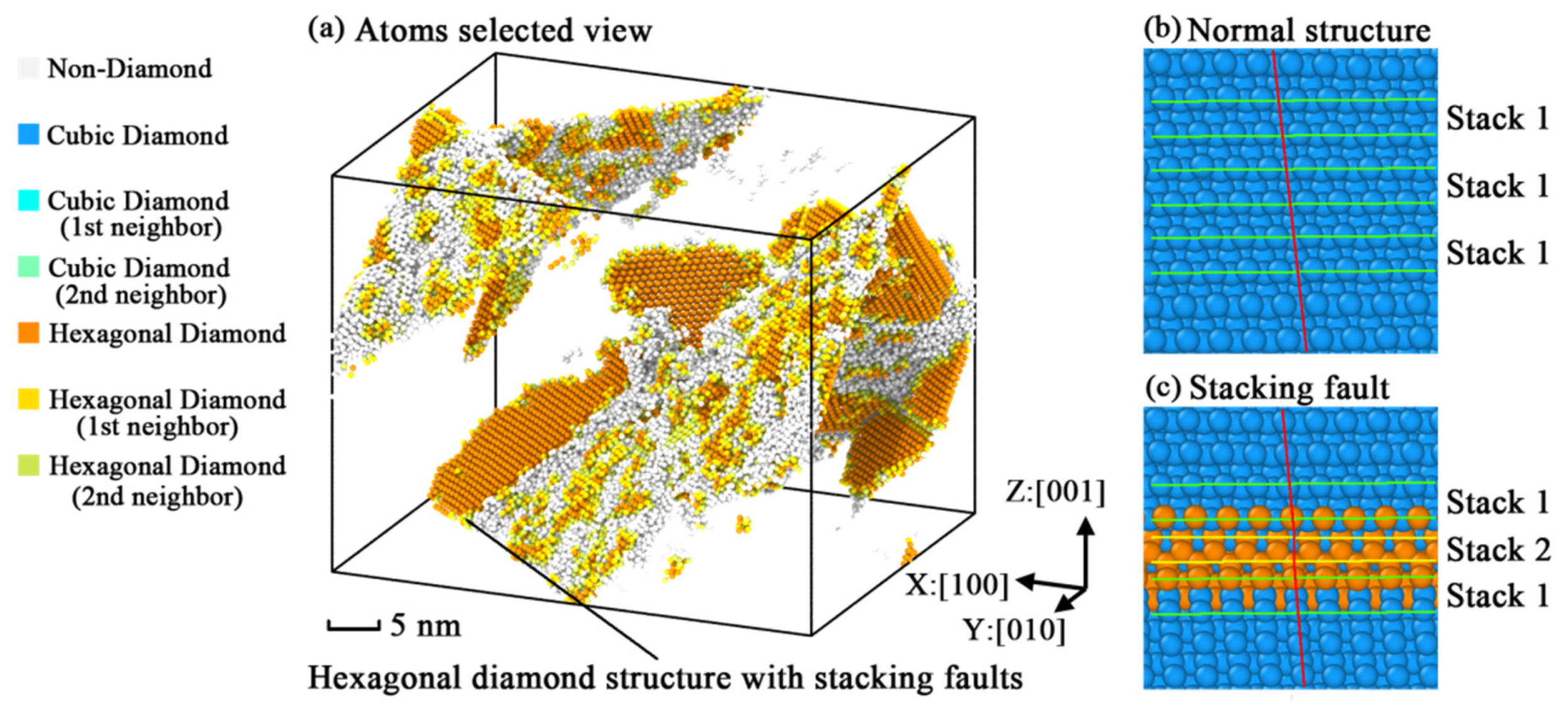
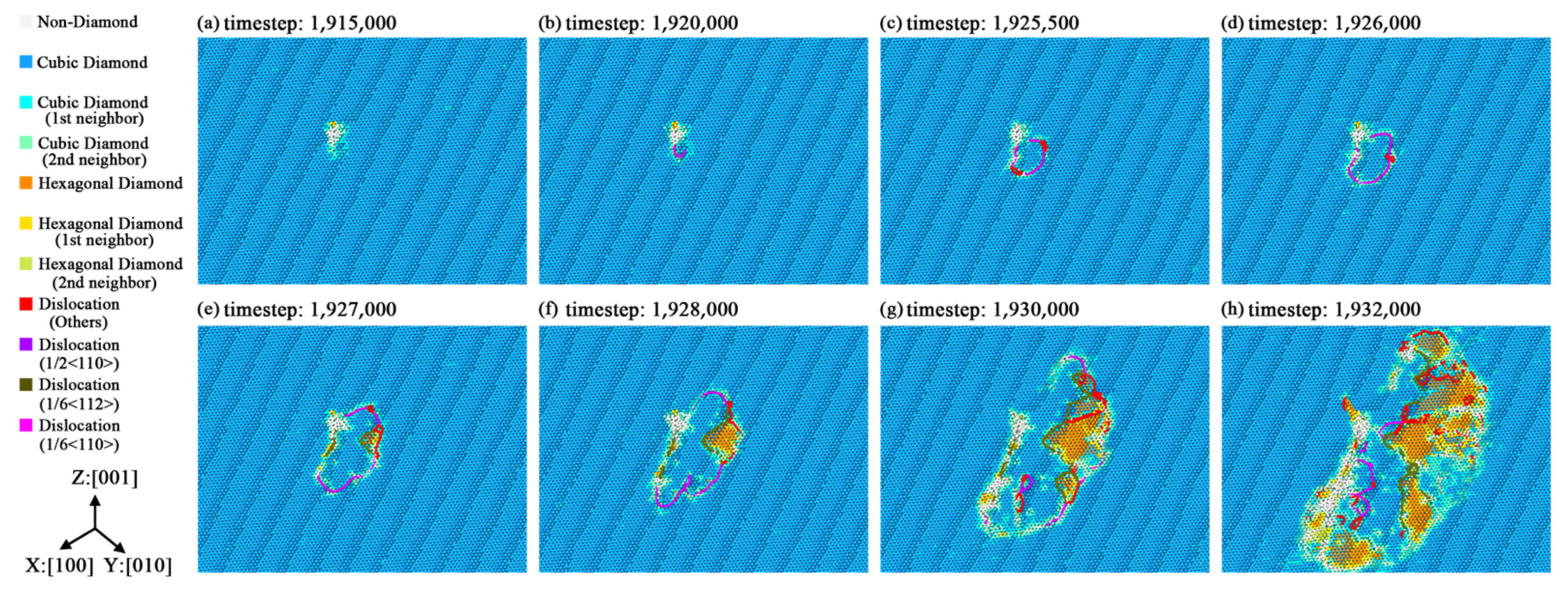
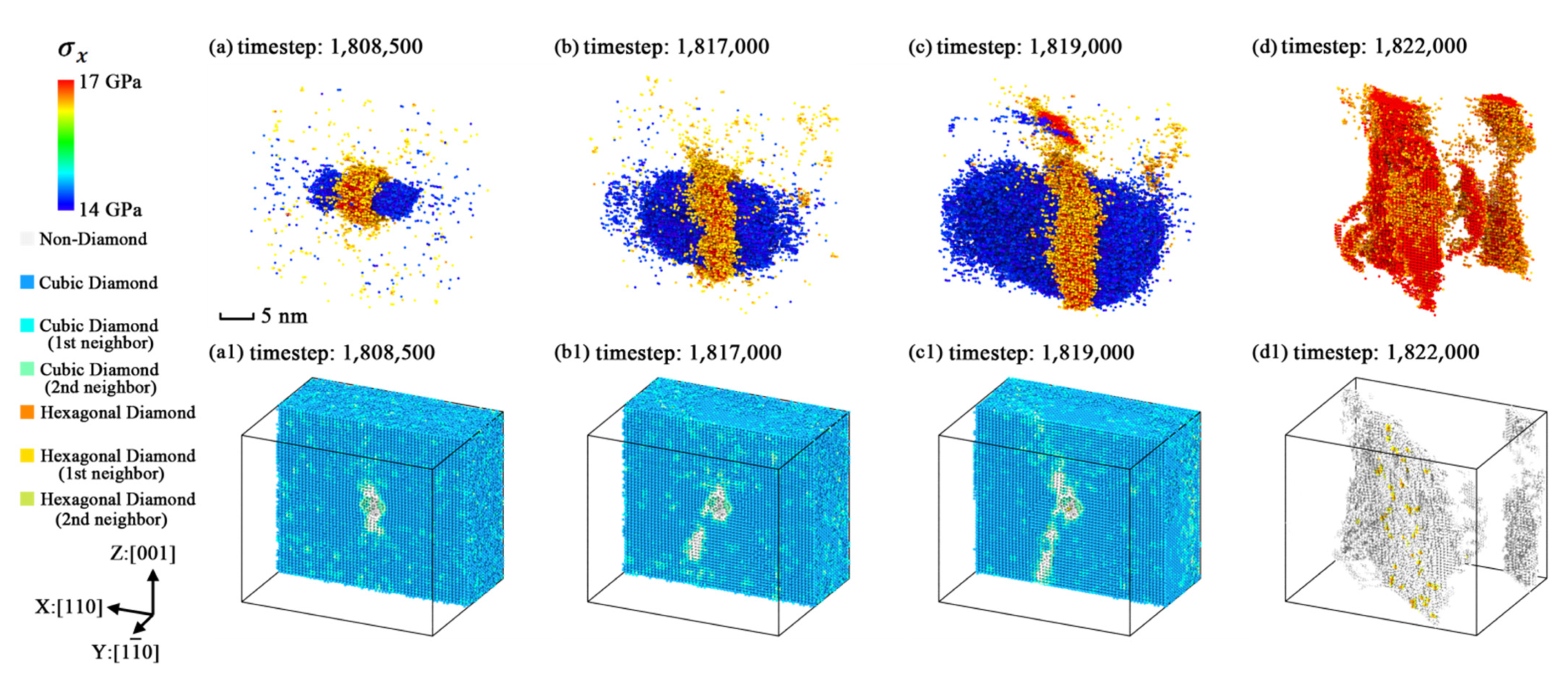
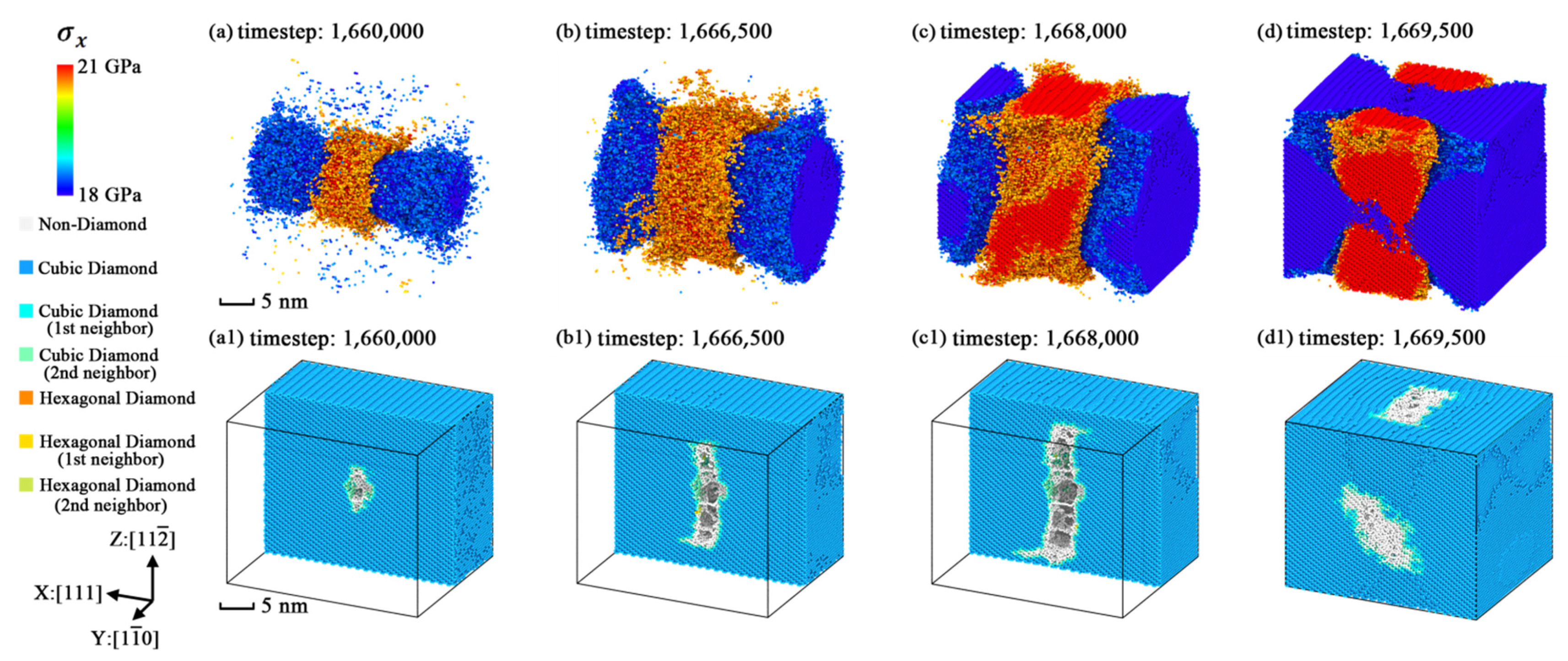
3.2. Anisotropy of Fracture Phenomena
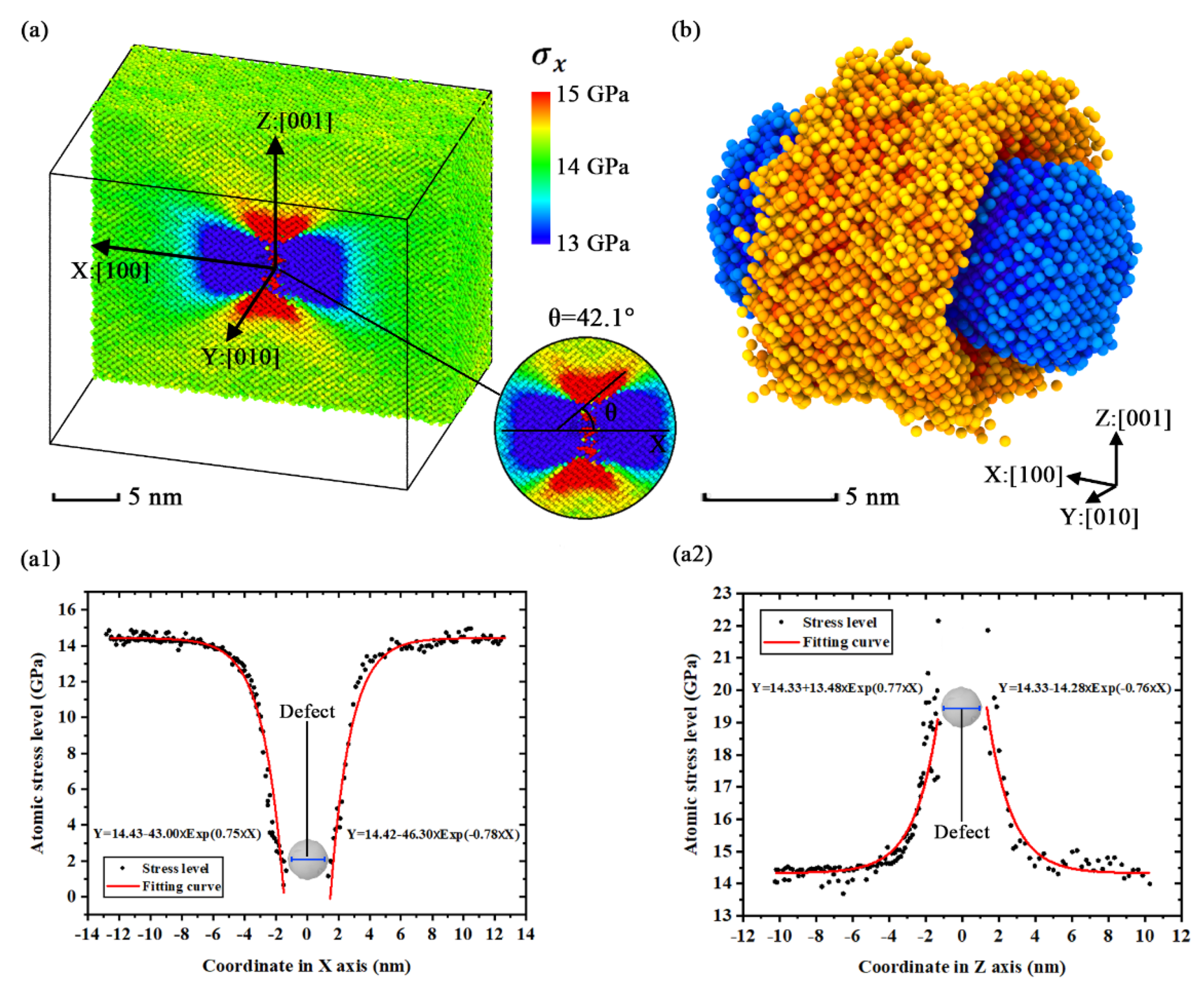
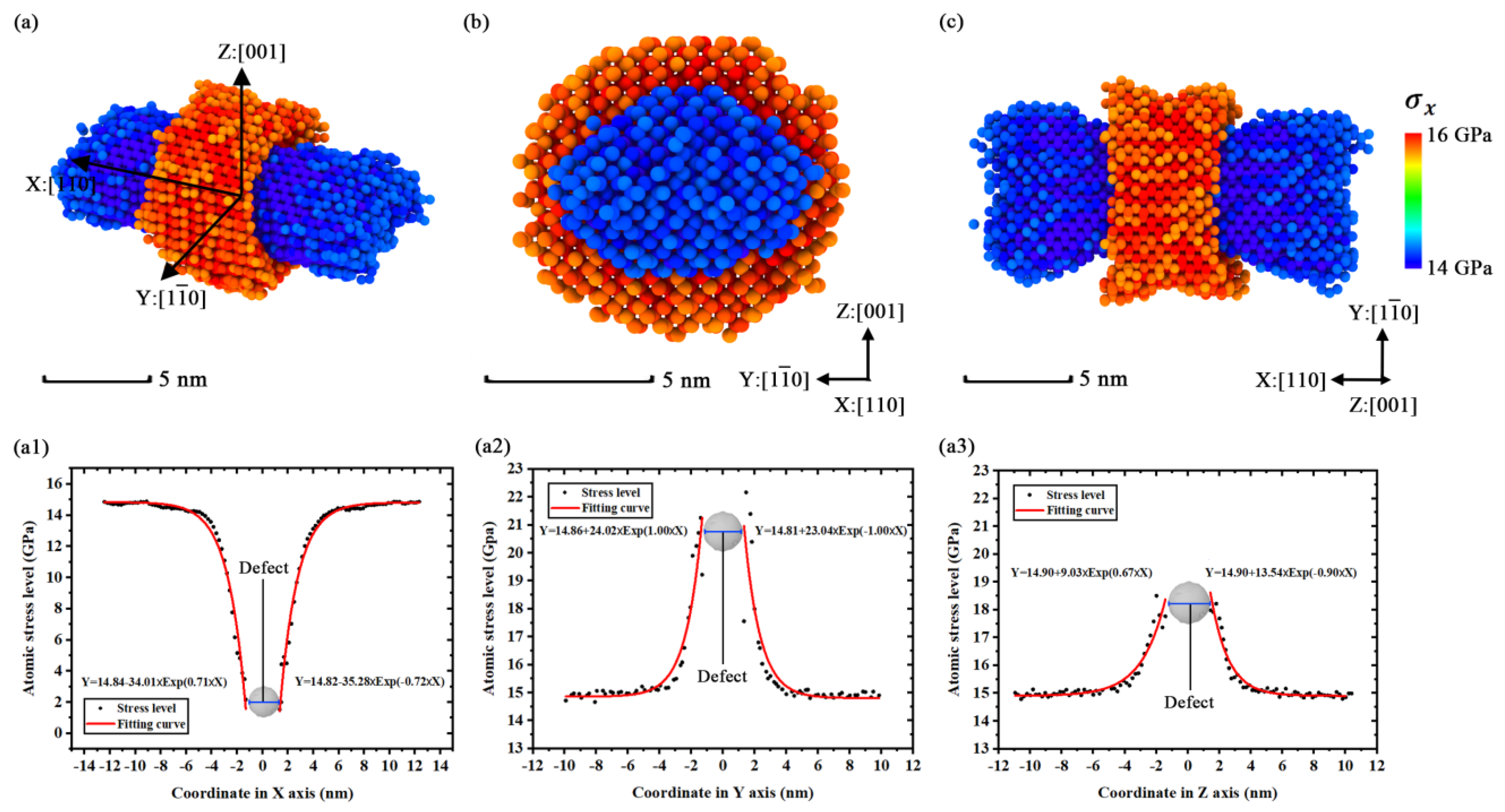
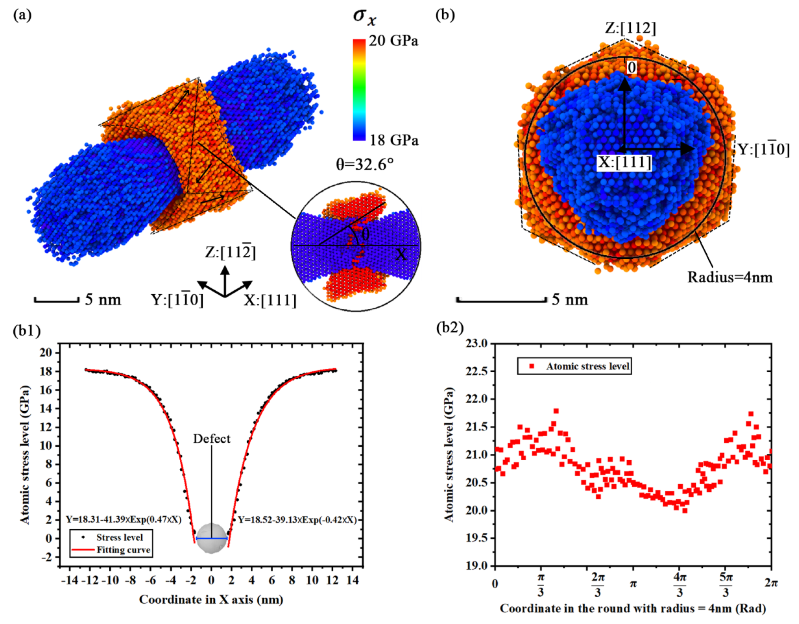
3.3. Anisotropy of Internal Stress
4. Conclusions
Author Contributions
Funding
Data Availability Statement
Acknowledgments
Conflicts of Interest
References
- Koga, Y.; Kurita, K. Floating zone silicon wafer bonded to Czochralski silicon substrate by surface-activated bonding at room temperature for infrared complementary metal-oxide-semiconductor image sensors. Jpn. J. Appl. Phys. 2021, 60, 015502. [Google Scholar] [CrossRef]
- Kuo, C.L.; Nien, Y.P.; Chiang, A.C.; Atsushi, H. Surface modification using assisting electrodes in wire electrical discharge machining for silicon wafer preparation. Materials 2021, 14, 1355. [Google Scholar] [CrossRef] [PubMed]
- Kang, R.K.; Zeng, Y.F.; Gao, S.; Dong, Z.G.; Guo, D.M. Surface layer damage of silicon wafers sliced by wire saw process. Adv. Mater. Res. 2013, 797, 685–690. [Google Scholar] [CrossRef]
- Sekhar, H.; Fukuda, T.; Tanahashi, K.; Takato, H.; Ono, H.; Sampei, Y.; Kobayashi, T. Mechanical strength problem of thin silicon wafers (120 and 140 µm) cut with thinner diamond wires (Si kerf 120→100 µm) for photovoltaic use. Mat. Sci. Semicond. Proc. 2020, 119, 105209. [Google Scholar] [CrossRef]
- Costa, E.C.; Xavier, F.A.; Knoblauch, R.; Binder, C.; Weingaertner, W.L. Effect of cutting parameters on surface integrity of monocrystalline silicon sawn with an endless diamond wire saw. Sol. Energy 2020, 207, 640–650. [Google Scholar] [CrossRef]
- Borrero-Lopez, O.; Vodenitcharova, T.; Hoffman, M. Anisotropy effects on the reliability of single-crystal silicon. Scripta Mater. 2010, 63, 997–1000. [Google Scholar] [CrossRef]
- Ebrahimi, F.; Kalwani, L. Fracture anisotropy in silicon single crystal. Mat. Sci. Eng. A-Struct. 1999, 268, 116–216. [Google Scholar] [CrossRef]
- Ebrahimi, F.; Hussain, S.I. Crack path in single-crystals. Scr. Mater. 1995, 32, 1507–1511. [Google Scholar] [CrossRef]
- Brookes, C.A.; Oneill, J.B.; Redfern, B.A.W. Anisotropy in hardness of single crystals. Proc. R. Soc. Lond. Ser. A-Math. Phys. Sci. 1971, 322, 73. [Google Scholar]
- Perez, R.; Gumbsch, P. Directional anisotropy in the cleavage fracture of silicon. Phys. Rev. Lett. 2000, 84, 5347–5350. [Google Scholar] [CrossRef] [Green Version]
- Moulins, A.; Ma, L.Y.; Dugnani, R.; Zednik, R.J. Dynamic crack modeling and analytical stress field analysis in single-crystal silicon using quantitative fractography. Theor. Appl. Fract. Mec. 2020, 109, 102693. [Google Scholar] [CrossRef]
- Mylvaganam, K.; Zhang, L. Effect of crystal orientation on the formation of bct-5 silicon. Comp. Mater. Sci. 2014, 81, 10–14. [Google Scholar] [CrossRef]
- George, A.; Michot, G. Dislocation loops at crack tips: Nucleation and growth-an experimental study in silicon. Mat. Sci. Eng. A-Struct. 1993, 164, 118–134. [Google Scholar] [CrossRef]
- Zhang, X.; Zhang, L.; Mironov, S.; Xiao, R.S.; Guo, L.; Huang, T. Effect of crystallographic orientation on structural response of silicon to femtosecond laser irradiation. Appl. Phys. A-Mater. 2021, 127, 196. [Google Scholar] [CrossRef]
- Liu, B.; Xu, Z.W.; Chen, C.; Li, R.; Gao, X.; Liang, L. Numerical and experimental investigation on ductile deformation and subsurface defects of monocrystalline silicon during nano-scratching. Appl. Surf. Sci. 2020, 528, 147034. [Google Scholar] [CrossRef]
- Rickhey, F.; Marimuthu, K.P.; Lee, K.; Lee, H. Indentation cracking of monocrystalline silicon considering fracture anisotropy. Theor. Appl. Fract. Mech. 2019, 100, 128–138. [Google Scholar] [CrossRef]
- Liu, X.; Devor, R.E.; Kapoor, S.G.; Ehmann, K.F. The mechanics of machining at the microscale: Assessment of the current state of the science. J. Manuf. Sci. Eng. 2015, 126, 5064–5070. [Google Scholar] [CrossRef]
- Komanduri, R.; Raff, L.M. A review on the molecular dynamics simulation of machining at the atomic scale. P. I. Mech. Eng. B-J. Eng. 2001, 215, 1639–1672. [Google Scholar] [CrossRef]
- Goel, S.; Luo, X.C.; Agrawal, A.; Reuben, R.L. Diamond machining of silicon: A review of advances in molecular dynamics simulation. Int. J. Mach. Tools Manuf. 2015, 88, 131–164. [Google Scholar] [CrossRef] [Green Version]
- Gumbsch, P.; Zhou, S.J.; Holian, B.L. Molecular dynamics investigation of dynamic crack stability. Phys. Rev. B 1997, 55, 3445–3455. [Google Scholar] [CrossRef]
- Wang, G.L.; Feng, Z.J.; Hu, Y.H.; Liu, J.; Zheng, Q.C. Effects of anisotropy on single crystal silicon in polishing non-continuous surface. Micromachines 2020, 11, 742. [Google Scholar] [CrossRef] [PubMed]
- Wu, H.; Melkote, S.N. Effect of crystal defects on mechanical properties relevant to cutting of multicrystalline solar silicon. Mat. Sci. Semicond. Proc. 2013, 16, 1416. [Google Scholar] [CrossRef]
- Korsós, F.; Roszol, L.; Jay, F.; Veirman, J.; Draoua, D.A.; Albaric, M.; Szarvas, T.; Kiss, Z.; Szabó, A.; Soczó, I.; et al. Efficiency limiting crystal defects in monocrystalline silicon and their characterization in production. Sol. Energy Mater. Sol. Cell 2018, 186, 217–226. [Google Scholar] [CrossRef]
- Menold, T.; Hadjixenophontos, E.; Lawitzki, R.; Schmitz, G.; Ametowobla, M. Crystal defects in monocrystalline silicon induced by spot laser melting. J. Appl. Phys. 2020, 127, 093102. [Google Scholar] [CrossRef]
- Pham, V.T.; Fang, T.H. Anisotropic mechanical strength, negative Poisson’s ratio and fracture mechanism of borophene with defects. Thin Solid Films 2020, 709, 138197. [Google Scholar] [CrossRef]
- Bagheripoor, M.; Klassen, R. The effect of crystal anisotropy and pre-existing defects on the incipient plasticity of Fcc single crystals during nanoindentation. Mech. Mater. 2020, 143, 103311. [Google Scholar] [CrossRef]
- Dong, S.H.; Xia, Y.X.; Huang, R.Y.; Zhao, J.H. Modulating mechanical anisotropy of two-dimensional materials by controlling their defects. Carbon 2019, 158, 77–88. [Google Scholar] [CrossRef]
- Wan, W.; Tang, C.X.; Qiu, A.; Xiang, Y.K. The size effects of point defect on the mechanical properties of monocrystalline silicon: A molecular dynamics study. Materials 2021, 14, 3011. [Google Scholar] [CrossRef]
- Balamane, H.; Halicioglu, T.; Tiller, W.A. Comparative study of silicon empirical interatomic potentials. Phys. Rev. B 1992, 46, 2250. [Google Scholar] [CrossRef] [PubMed]
- Tersoff, J. Empirical interatomic potential for silicon with improved elastic properties. Phys. Rev. B 1988, 38, 9902. [Google Scholar] [CrossRef]
- Zhou, N.G.; Hu, Q.F.; Xu, W.X.; Li, K.; Zhou, L. A comparative study of different potentials for molecular dynamics simulations of melting process of silicon. Acta Phys. Sin-Ch. Ed. 2013, 62, 146401. [Google Scholar]
- Zhou, Z.Y.; Wang, T.B.; Cheng, Z.N. Molecular dynamics study on local structure of molten silicon. Acta Phys. Sin-Ch. Ed. 1999, 48, 2239–2240. [Google Scholar]
- Erhart, P.; Albe, K. Analytical potential for atomistic simulations of silicon, carbon, and silicon carbide. Phys. Rev. B 2005, 71, 035211. [Google Scholar] [CrossRef] [Green Version]
- Nielsen, O.H.; Martin, R.M. Stresses in semiconductors: Ab initio calculations on Si, Ge, and GaAs. Phys. Rev. B 1985, 32, 3792. [Google Scholar] [CrossRef]
- Lenosky, T.J.; Kress, J.D.; Kwon, I.; Voter, A.F.; Edwards, B.; Yang, D.F.; Yang, S.; Adams, J.B. Highly optimized tight-binding model of silicon. Phys. Rev. B 1997, 55, 1528. [Google Scholar] [CrossRef]
- Tersoff, J. Modeling solid-state chemistry: Interatomic potentials for multicomponent systems. Phys. Rev. B 1989, 39, 5566. [Google Scholar] [CrossRef] [PubMed]
- Justo, J.F.; Bazant, M.Z.; Kaxiras, E.; Bulatov, V.V.; Yip, S. Interatomic potential for silicon defects and disordered phases. Phys. Rev. B 1998, 58, 2539. [Google Scholar] [CrossRef] [Green Version]
- Berendsen, H.J.C.; Postma, J.P.M.; VanGunsteren, W.F.; DiNola, A.; Haak, J.R. Molecular dynamics with coupling to an external bath. J. Chem. Phys. 1984, 81, 3684. [Google Scholar] [CrossRef] [Green Version]
- Stukowski, A. Visualization and analysis of atomistic simulation data with ovito–the open visualization tool. Model. Simul. Mater. Sci. Eng. 2010, 18, 015012. [Google Scholar] [CrossRef]
- Amini, H.; Simchi, A.; Kokabi, A.H. Effects of crystal orientation on the tensile and shear deformation of nickel-silicon interfaces: A molecular dynamics simulation. Mat. Sci. Eng. A-Struct. 2012, 543, 217–223. [Google Scholar] [CrossRef]
- Tsai, Y.L.; Mecholsky, J.J. Fractal fracture of single-crystal silicon. J. Mater. Res. 1991, 6, 1248–1263. [Google Scholar] [CrossRef]
- Liu, J.; Yuan, H. The evolution and failure mechanism of lithium metal anode under practical working conditions. J. Energy Chem. 2020, 48, 440–441. [Google Scholar] [CrossRef]
- Herold, S.; Acker, J. Lattice strain enhanced acidic etching on as cut sawn silicon wafer. Mat. Sci. Semicond. Proc. 2021, 123, 105575. [Google Scholar] [CrossRef]
- Chevrier, J. Experimental-analysis of river patterns in silicon brittle fractures. J. Phys. I 1995, 5, 675–683. [Google Scholar] [CrossRef] [Green Version]
- Tsoutsouva, M.G.; Regula, G.; Ryningen, B.; Vullum, P.E.; Mangelinck-Noel, N.; Stokkan, G. Dynamic observation of dislocation evolution and interaction with twin boundaries in silicon crystal growth using in-situ synchrotron X-ray diffraction imaging. Acta Mater. 2021, 210, 116819. [Google Scholar] [CrossRef]
- Sumino, K.; Yonenaga, I. Difference in the mechanical strengths of dislocation-free crystals of Czochralski silicon and Float-zone silicon. Jpn. J. Appl. Phys. 1981, 20, L685–L688. [Google Scholar] [CrossRef]
- Chiao, Y.H.; Clarke, D.R. Direct observation of dislocation emission from crack tips in silicon at high-temperatures. Acta Mater. 1989, 37, 203–219. [Google Scholar] [CrossRef]
- Thaulow, C.; Sen, D.P.J.; Buehler, M.J. Atomistic study of the effect of crack tip ledges on the nucleation of dislocations in silicon single crystals at elevated temperature. Mat. Sci. Eng. A-Struct. 2011, 528, 4357–4364. [Google Scholar] [CrossRef]
- Zenari, M.; Buffolo, M.; De Santi, C.; Norman, J.; Meneghesso, G.; Bowers, J.E.; Zanoni, E.; Meneghini, M. Identification of dislocation-related and point-defects in III-As layers for silicon photonics applications. J. Phys. D Appl. Phys. 2021, 54, 285101. [Google Scholar] [CrossRef]
- Atrash, F.; Hashibon, A.; Gumbsch, P.; Sherman, D. Phonon emission induced dynamic fracture phenomena. Phys. Rev. Lett. 2011, 106, 085502. [Google Scholar] [CrossRef]


| Model Type | Crystal Orientation | Axial Length/nm | Atoms Per Single Cell | Atoms Amount | ||||
|---|---|---|---|---|---|---|---|---|
| X Axis | Y Axis | Z Axis | X Axis | Y Axis | Z Axis | |||
| [100] Simulation Model | [100] | [010] | [001] | 21.7 | 21.7 | 21.7 | 8 | 512,000 |
| [110] Simulation Model | [110] | [001] | 21.5 | 21.7 | 21.5 | 16 | 501,760 | |
| [111] Simulation Model | [111] | 21.6 | 21.5 | 21.3 | 32 | 494,592 | ||
| Postfix of Model ID | “-1” | “-2” | “-3” | “-4” | “-5” | “-6” |
|---|---|---|---|---|---|---|
| Defect Size/Atoms | 0 | 1 | 123 | 281 | 2149 | 4229 |
| Defect Radius/nm | 0.000 | 0.118 | 0.815 | 1.086 | 2.172 | 2.715 |
| Elastic Constants | Expt. [33] | QM Methods | Molecular Dynamics Simulation | ||||
|---|---|---|---|---|---|---|---|
| DFT [34] | TB [35] | Tersoff T2 [30] | Tersoff T3 [36] | SW [29] | EDIP [37] | ||
| C11 (GPa) | 168 | 159 | 167 | 166 | 143 | 162 | 175 |
| C12 (GPa) | 65 | 61 | 67 | 65 | 75 | 82 | 62 |
| C44 (GPa) | 80 | 85 | 75 | 77 | 69 | 60 | 71 |
| Crystal Orientation | Young’s Modulus/GPa | Yield Strength/GPa | Single Defect Decay/GPa |
|---|---|---|---|
| [100] | 111.2 | 18.2 | 1.4 |
| [110] | 148.2 | 19.5 | 0.9 |
| [111] | 163.9 | 23.4 | 0.5 |
| Crystal Orientation | σ/GPa | A/GPa | R/Atoms−1 |
|---|---|---|---|
| [100] | 12.05 ± 0.46 | 5.41 ± 0.64 | −0.0051 ± 0.0015 |
| [110] | 13.20 ± 0.44 | 5.82 ± 0.62 | −0.0054 ± 0.0015 |
| [111] | 15.35 ± 0.47 | 7.74 ± 0.66 | −0.0065 ± 0.0015 |
Publisher’s Note: MDPI stays neutral with regard to jurisdictional claims in published maps and institutional affiliations. |
© 2021 by the authors. Licensee MDPI, Basel, Switzerland. This article is an open access article distributed under the terms and conditions of the Creative Commons Attribution (CC BY) license (https://creativecommons.org/licenses/by/4.0/).
Share and Cite
Wan, W.; Tang, C.; Zhang, J.; Zhou, L. General Molecular Dynamics Approach to Understand the Mechanical Anisotropy of Monocrystalline Silicon under the Nanoscale Effects of Point Defect. Nanomaterials 2021, 11, 1965. https://doi.org/10.3390/nano11081965
Wan W, Tang C, Zhang J, Zhou L. General Molecular Dynamics Approach to Understand the Mechanical Anisotropy of Monocrystalline Silicon under the Nanoscale Effects of Point Defect. Nanomaterials. 2021; 11(8):1965. https://doi.org/10.3390/nano11081965
Chicago/Turabian StyleWan, Wei, Changxin Tang, Jianjie Zhang, and Lang Zhou. 2021. "General Molecular Dynamics Approach to Understand the Mechanical Anisotropy of Monocrystalline Silicon under the Nanoscale Effects of Point Defect" Nanomaterials 11, no. 8: 1965. https://doi.org/10.3390/nano11081965