
Fabrication of Piezoelectric ZnO Nanowires Energy Harvester on Flexible Substrate Coated with Various Seed Layer Structures

 , and
, and 
Abstract
:1. Introduction
2. Experimental
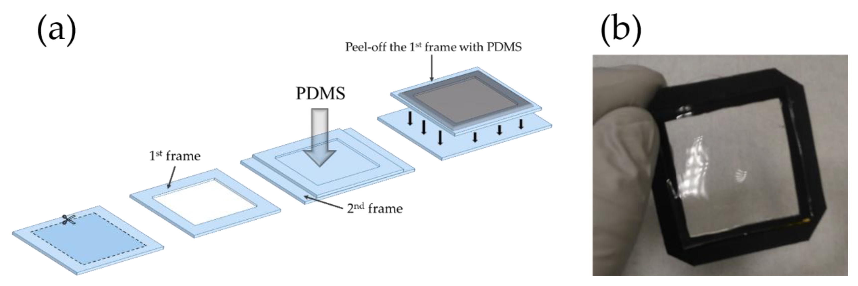
2.1. Flexible Substrate Preparation
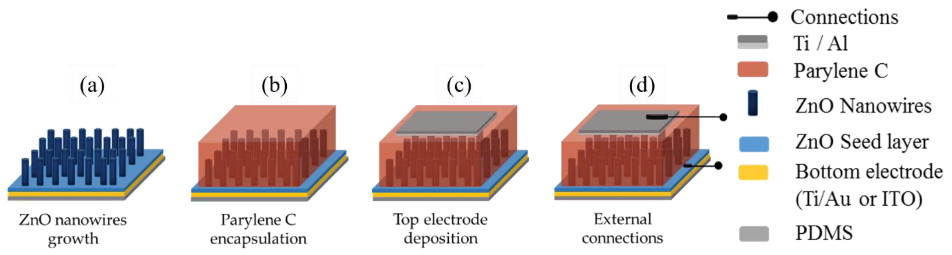
2.2. Bottom Electrode-Seed Layers Preparation (ITO/ZnO, Ti/Au/ZnO) and Growth of the ZnO Nanowires
2.3. Fabrication of PENG Device
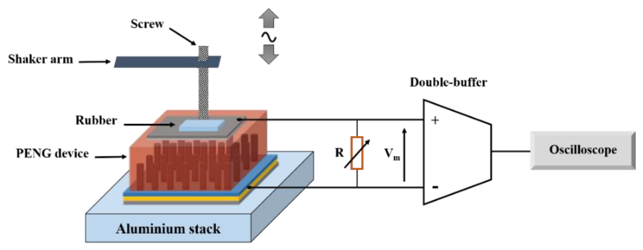
2.4. Characterization Techniques
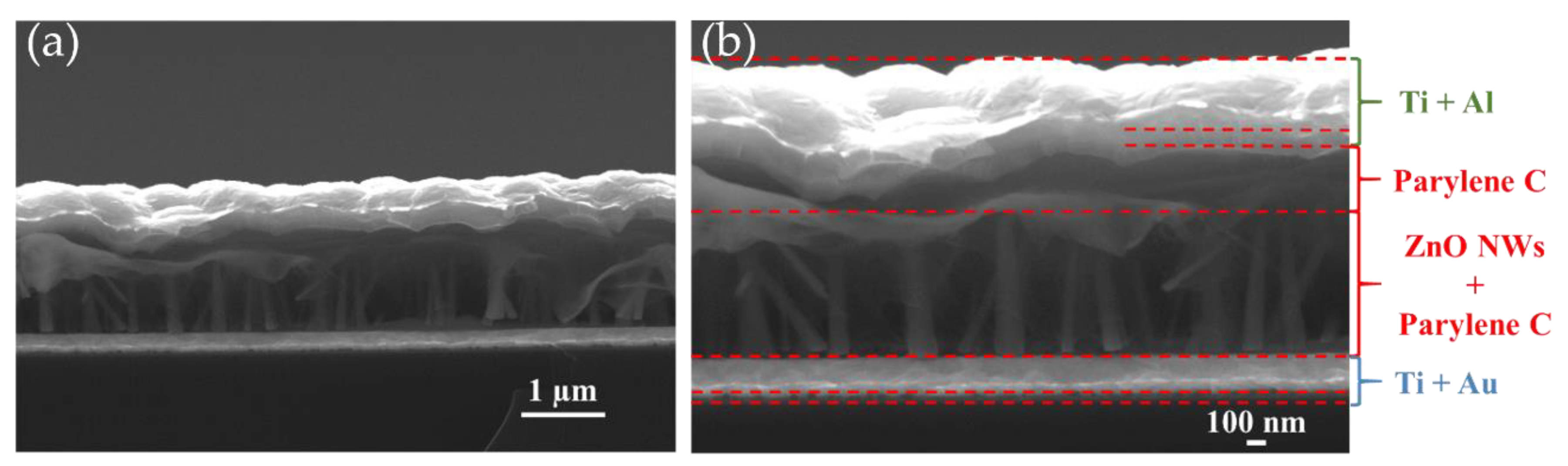
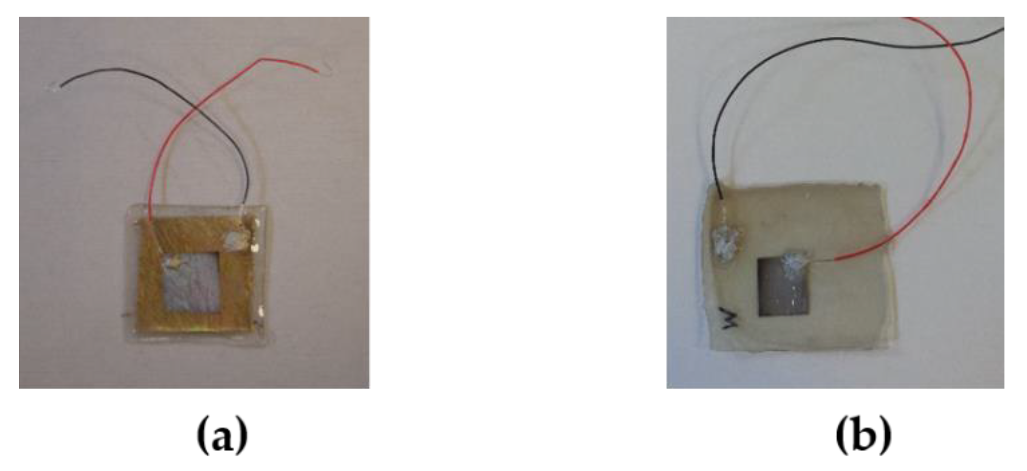
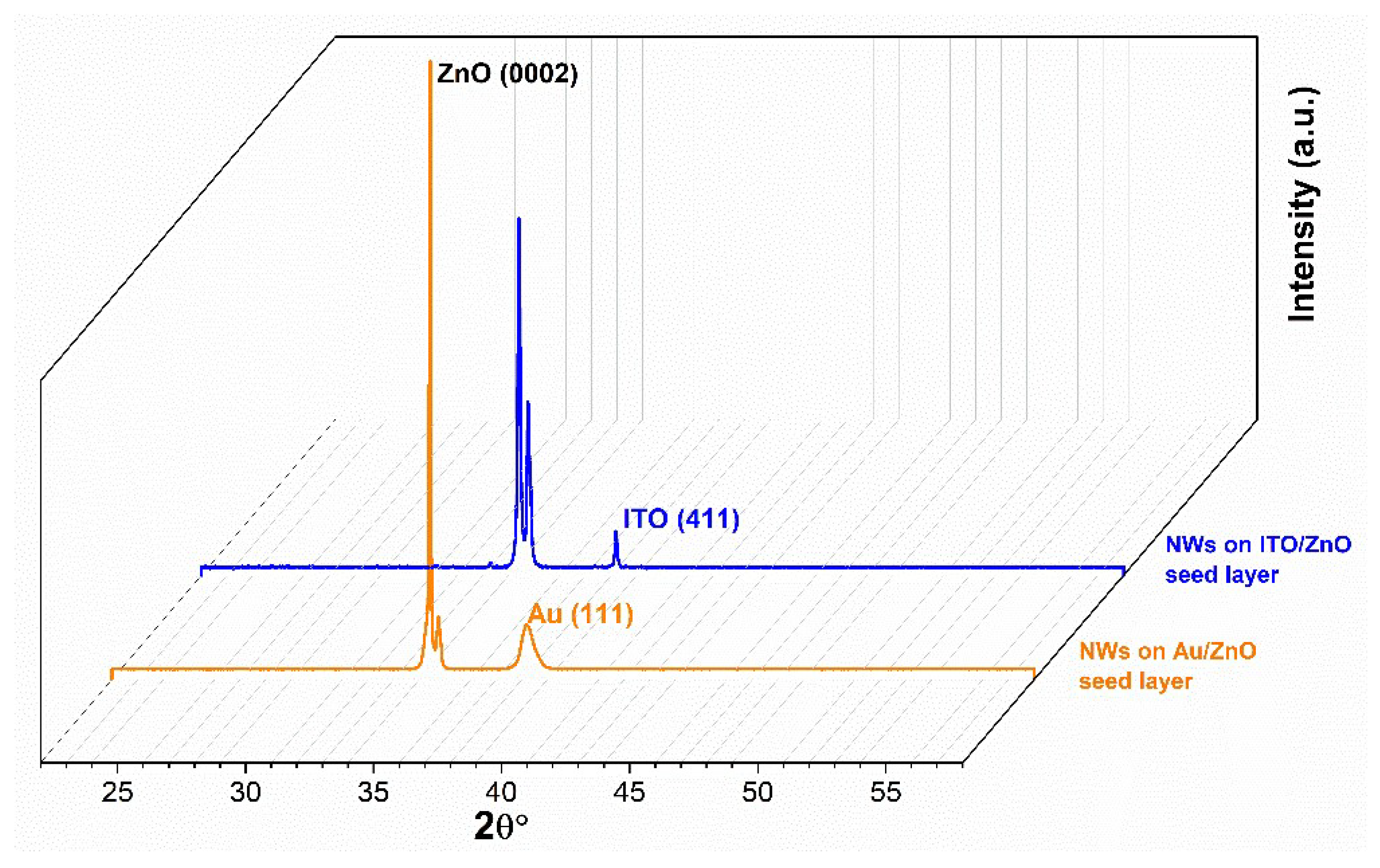
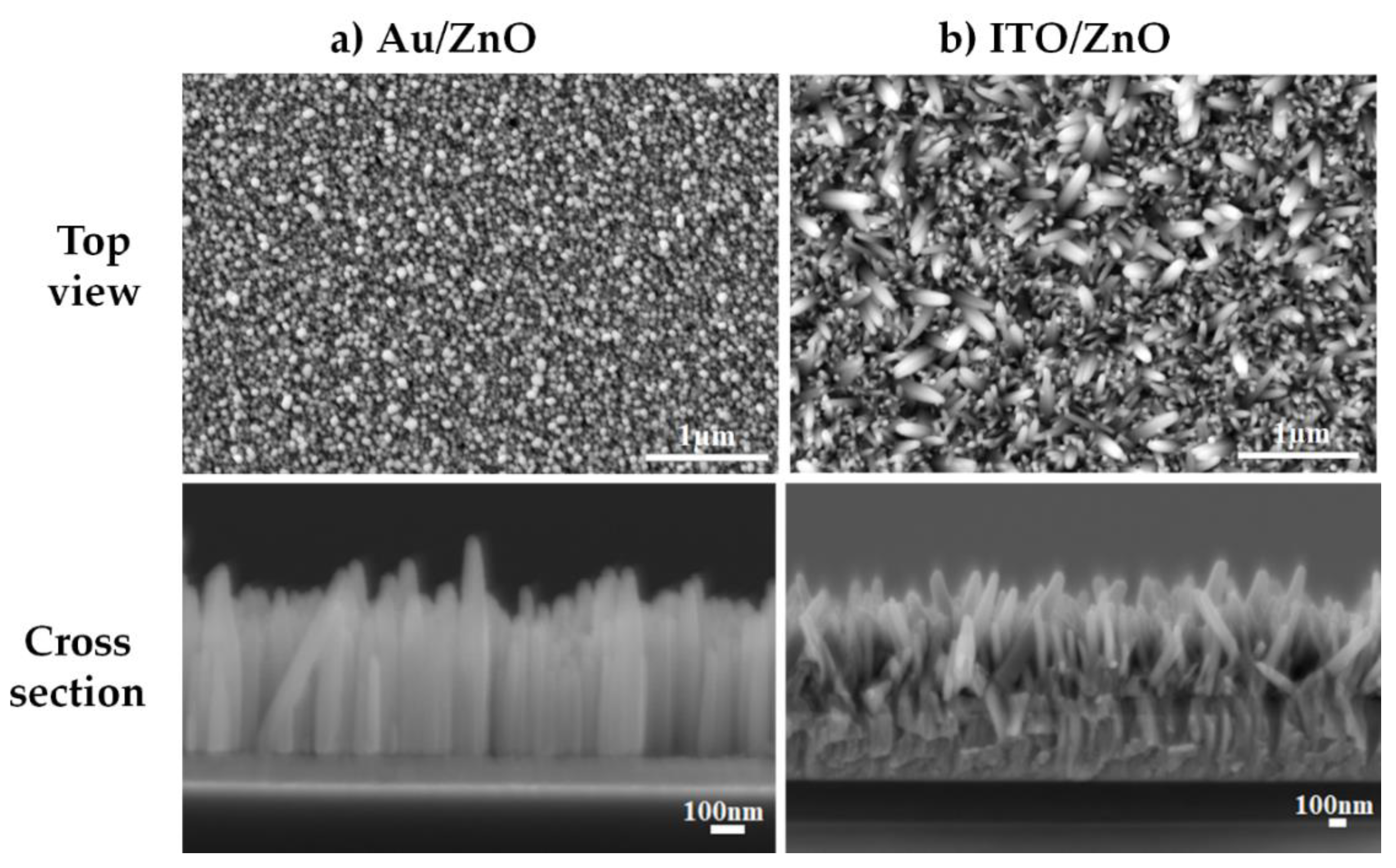
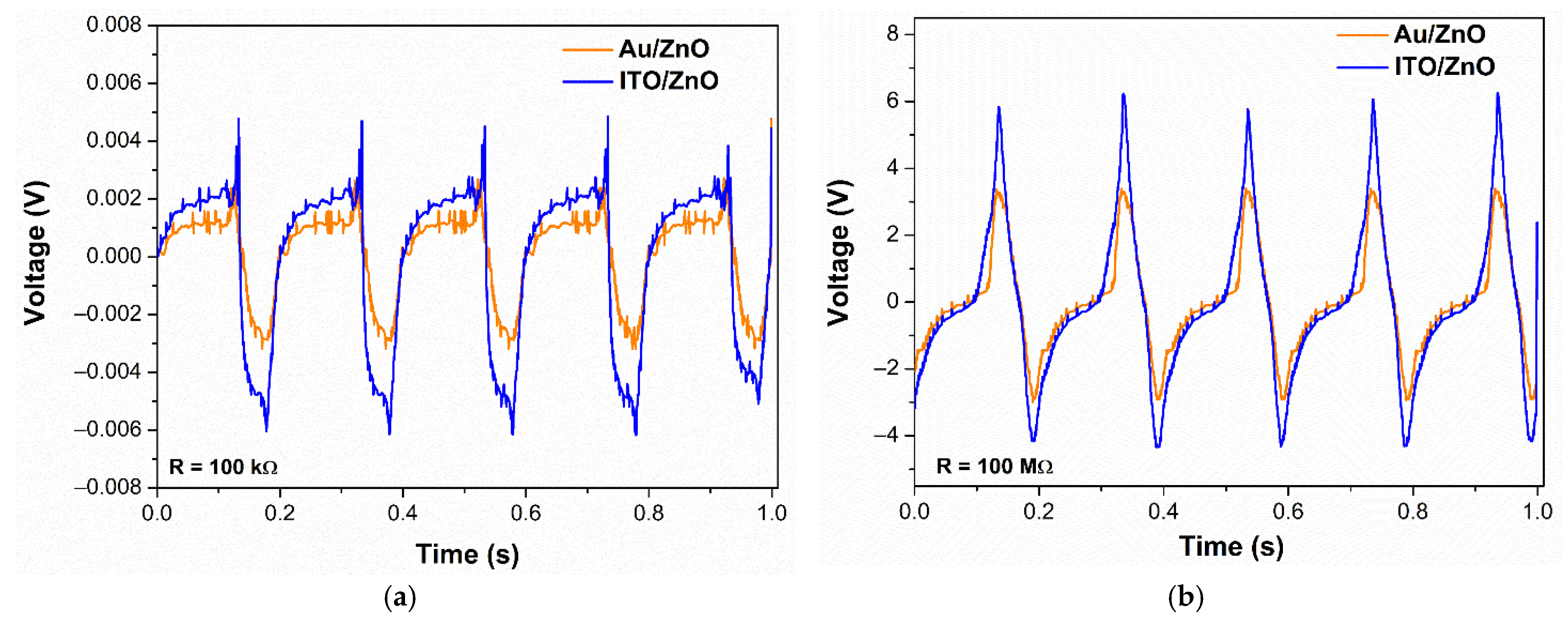
3. Results and Discussion
4. Conclusions
Author Contributions
Funding
Institutional Review Board Statement
Informed Consent Statement
Data Availability Statement
Conflicts of Interest
References
- Sripadmanabhan Indira, S.; Aravind Vaithilingam, C.; Oruganti, K.S.P.; Mohd, F.; Rahman, S. Nanogenerators as a Sustain-able Power Source: State of Art, Applications, and Challenges. Nanomaterials 2019, 9, 773. [Google Scholar] [CrossRef] [PubMed] [Green Version]
- Hu, Y.; Wang, Z.L. Recent progress in piezoelectric nanogenerators as a sustainable power source in self-powered systems and active sensors. Nano Energy 2015, 14, 3–14. [Google Scholar] [CrossRef] [Green Version]
- Dagdeviren, C.; Yang, B.D.; Su, Y.; Tran, P.L.; Joe, P.; Anderson, E.; Xia, J.; Doraiswamy, V.; Dehdashti, B.; Feng, X.; et al. Conformal piezoelectric energy harvesting and storage from motions of the heart, lung, and diaphragm. Proc. Natl. Acad. Sci. USA 2014, 111, 1927–1932. [Google Scholar] [CrossRef] [Green Version]
- Ye, S.; Cheng, C.; Chen, X.; Chen, X.; Shao, J.; Zhang, J.; Hu, H.; Tian, H.; Li, X.; Ma, L.; et al. High-performance piezoelec-tric nanogenerator based on microstructured P(VDF-TrFE)/BNNTs composite for energy harvesting and radiation protection in space. Nano Energy 2019, 60, 701–714. [Google Scholar] [CrossRef]
- Liu, Y.; Wang, L.; Zhao, L.; Yu, X.; Zi, Y. Recent progress on flexible nanogenerators toward self-powered systems. InfoMat 2020, 2, 318–340. [Google Scholar] [CrossRef] [Green Version]
- Fan, F.R.; Tang, W.; Wang, Z.L. Flexible Nanogenerators for Energy Harvesting and Self-Powered Electronics. Adv. Mater. 2016, 28, 4283–4305. [Google Scholar] [CrossRef] [PubMed]
- Wang, Z.L.; Song, J.H. Piezoelectric Nanogenerators Based on Zinc Oxide Nanowire Arrays. Science 2006, 312, 42–46. [Google Scholar] [CrossRef]
- Borysiewicz, M.A. ZnO as a Functional Material, a Review. Crystals 2019, 9, 505. [Google Scholar] [CrossRef] [Green Version]
- Fakhri, P.; Amini, B.; Bagherzadeh, R.; Kashfi, M.; Latifi, M.; Yavari, N.; Kani, S.A.; Kong, L. Flexible hybrid structure piezo-electric nanogenerator based on ZnO nanorod/PVDF nanofibers with improved output. RSC Adv. 2019, 9, 17–23. [Google Scholar] [CrossRef] [Green Version]
- Tlemcani, T.S.; Justeau, C.; Nadaud, K.; Poulin-Vittrant, G.; Alquier, D. Deposition Time and Annealing Effects of ZnO Seed Layer on Enhancing Vertical Alignment of Piezoelectric ZnO Nanowires. Chemosensors 2019, 7, 7. [Google Scholar] [CrossRef] [Green Version]
- Justeau, C.; Tlemcani, T.S.; Poulin-Vittrant, G.; Nadaud, K.; Alquier, D. A Comparative Study on the Effects of Au, ZnO and AZO Seed Layers on the Performance of ZnO Nanowire-Based Piezoelectric Nanogenerators. Materials 2019, 12, 2511. [Google Scholar] [CrossRef] [Green Version]
- Boubenia, S.; Dahiya, A.S.; Poulin-Vittrant, G.; Morini, F.; Nadaud, K.; Alquier, D. A facile hydrothermal approach for the density tunable growth of ZnO nanowires and their electrical characterizations. Sci. Rep. 2017, 7, 1–10. [Google Scholar] [CrossRef] [PubMed] [Green Version]
- Poulin-Vittrant, G.; Oshman, C.; Opoku, C.; Dahiya, A.S.; Camara, N.; Alquier, D.; Tran Huu Hue, L.P.; Lethiecq, M. Fabri-cation and Characterization of ZnO Nanowire-based Piezoelectric Nanogenerators for Low Frequency Mechanical Energy Harvesting. Phys. Procedia 2015, 70, 909–913. [Google Scholar] [CrossRef] [Green Version]
- Ou, C.; Sanchez-Jimenez, P.E.; Datta, A.; Boughey, F.L.; Whiter, R.A.; Sahonta, S.L.; Kar-Narayan, S. Template-assisted hy-drothermal growth of aligned zinc oxide nanowires for piezoelectric energy harvesting applications. Appl. Mater. Interfaces 2016, 8, 13678–13683. [Google Scholar] [CrossRef] [PubMed]
- Dahiya, A.S.; Morini, F.; Boubenia, S.; Justeau, C.; Nadaud, K.; Rajeev, K.P.; Alquier, D.; Poulin-Vittrant, G. Zinc oxide nanowire-parylene nanocomposite based stretchable piezoelectric nanogenerators for self-powered wearable electronics. J. Phys. Conf. Ser. 2018, 1052, 012028. [Google Scholar] [CrossRef]
- Boubenia, S. Générateurs Piézoélectriques à Base de Nanofils Piézo-Semiconducteurs: Modélisation, Fabrication et Caractérisation. Ph.D. Thesis, University of Tours, Tours, France, 2019. [Google Scholar]
- Dahiya, A.S.; Morini, F.; Boubenia, S.; Nadaud, K.; Alquier, D.; Poulin-Vittrant, G. Organic/Inorganic Hybrid Stretchable Piezoelectric Nanogenerators for Self-Powered Wearable Electronics. Adv. Mater. Technol. 2018, 3, 1700249. [Google Scholar] [CrossRef] [Green Version]
- Lien, S.-Y.; Nautiyal, A.; Lee, S.J. Optoelectronic Properties of Indium–Tin Oxide Films Deposited on Flexible and Transparent Poly(dimethylsiloxane) Substrate. Jpn. J. Appl. Phys. 2013, 52, 115801. [Google Scholar] [CrossRef]
- Casper, M.D.; Gözen, A.Ö.; Dickey, M.D.; Genzer, J.; Maria, J.-P. Surface wrinkling by chemical modification of poly(dimethylsiloxane)-based networks during sputtering. Soft Matter 2013, 9, 7797–7803. [Google Scholar] [CrossRef]
- Ghayour, H.; Rezaie, H.R.; Mirdamadi, S.; Nourbakhsh, A.A. The effect of seed layer thickness on alignment and morphol-ogy of ZnO nanorods. Vaccum 2011, 86, 101–105. [Google Scholar] [CrossRef]
- Guillemin, S.; Consonni, V.; Appert, E.; Puyoo, E.; Rapenne, L.; Roussel, H. Critical Nucleation Effects on the Structural Rela-tionship Between ZnO Seed Layer and Nanowires. J. Phys. Chem. C 2012, 116, 25106–25111. [Google Scholar] [CrossRef]
- Elzein, B.; Yao, Y.; Barham, A.S.; Dogheche, E.; Jabbour, G.E. Toward the Growth of Self-Catalyzed ZnO Nanowires Perpen-dicular to the Surface of Silicon and Glass Substrates, by Pulsed Laser Deposition. Materials 2020, 13, 4427. [Google Scholar] [CrossRef]
- Gorham, W.F. A New, General Synthetic Method for the Preparation of Linear Poly-p-xylylenes. J. Polym. Sci. Part A-1 Polym. Chem. 1966, 4, 3027–3039. [Google Scholar] [CrossRef]
- Yang, D.; Qiu, Y.; Jiang, Q.; Guo, Z.; Song, W.; Xu, J.; Zong, Y.; Feng, Q.; Sun, X. Patterned growth of ZnO nanowires on flexible substrates for enhanced performance of flexible piezoelectric nanogenerators. Appl. Phys. Lett. 2017, 110, 063901. [Google Scholar] [CrossRef]
- Lee, K.Y.; Bae, J.; Kim, S.; Lee, J.-H.; Yoon, G.C.; Gupta, M.K.; Kim, S.; Kim, H.; Park, J.; Kim, S.-W. Depletion width engineering via surface modification for high performance semiconducting piezoelectric nanogenerators. Nano Energy 2014, 8, 165–173. [Google Scholar] [CrossRef]
- Nadaud, K.; Morini, F.; Dahiya, A.S.; Justeau, C.; Boubenia, S.; Rajeev, K.P.; Alquier, D.; Poulin-Vittrant, G. Double buffer circuit for the characterization of piezoelectric nanogenerators based on ZnO nanowires. Appl. Phys. Lett. 2018, 112, 063901. [Google Scholar] [CrossRef]
- Giri, P.; Dhara, S.; Chakraborty, R. Effect of ZnO seed layer on the catalytic growth of vertically aligned ZnO nanorod arrays. Mater. Chem. Phys. 2010, 122, 18–22. [Google Scholar] [CrossRef]
- Li, S.Y.; Lee, C.Y.; Tseng, T.Y. Copper-catalyzed ZnO nanowires on silicon (1 0 0) grown by vapor–liquid–solid process. J. Cryst. Growth 2003, 247, 357–362. [Google Scholar] [CrossRef]
- Van den Heever, T.S.; Perold, W.J. Comparing three different energy harvesting circuits for a ZnO nanowire based nano-generator. Smart Mater. Struct. 2013, 22, 105029. [Google Scholar] [CrossRef]
- Dahiya, A.S.; Thireau, J.; Boudaden, J.; Lal, S.; Gulzar, U.; Zhang, Y.; Gil, T.; Azemard, N.; Ramm, P.; Kiessling, T.; et al. Review—Energy Autonomous Wearable Sensors for Smart Healthcare: A Review. J. Electrochem. Soc. 2020, 167, 037516. [Google Scholar] [CrossRef]
- Schmid, H.; Wolf, H.; Allenspach, R.; Riel, H.; Karg, S.; Michel, B.; Delamarche, E. Preparation of Metallic Films on Elasto-meric Stamps and Their Application for Contact Processing and Contact Printing. Adv. Funct. Mater. 2003, 13, 145–153. [Google Scholar] [CrossRef]
- Kim, T.-W.; Lee, J.-S.; Kim, Y.-C.; Joo, Y.-C.; Kim, B.-J. Bending Strain and Bending Fatigue Lifetime of Flexible Metal Electrodes on Polymer Substrates. Materials 2019, 12, 2490. [Google Scholar] [CrossRef] [PubMed] [Green Version]
- Huck, W.T.S.; Bowden, N.; Onck, P.; Pardoen, T.; Hutchinson, A.J.W.; Whitesides, G.M. Ordering of Spontaneously Formed Buckles on Planar Surfaces. Langmuir 2000, 16, 3497–3501. [Google Scholar] [CrossRef]
- Sekitani, T. Someya, Stretchable, Large-area Organic Electronics. Adv. Mater. 2010, 22, 2228–2246. [Google Scholar] [CrossRef] [PubMed]
- Gupta, R. Fabrication of stretchable compliant electrodes on PDMS with Au nanoparticles. Bull. Mater. Sci. 2018, 41, 114. [Google Scholar] [CrossRef] [Green Version]
- Gao, Y.; Wang, Z.L. Electrostatic Potential in a Bent Piezoelectric Nanowire. The Fundamental Theory of Nanogenerator and Nanopiezotronics. Nano Lett. 2007, 7, 2499–2505. [Google Scholar] [CrossRef]
- Zhu, G.; Yang, R.; Wang, S.; Wang, Z.L. Flexible High-Output Nanogenerator Based on Lateral ZnO Nanowire Array. Nano Lett. 2010, 10, 3151–3155. [Google Scholar] [CrossRef] [Green Version]
- Lin, L.; Hu, Y.; Xu, C.; Zhang, Y.; Zhang, R.; Wen, X.; Wang, Z.L. Transparent flexible nanogenerator as self-powered sensor for transportation monitoring. Nano Energy 2013, 2, 75–81. [Google Scholar] [CrossRef]
- Hinchet, R.; Lee, S.; Ardila, G.; Montès, L.; Mouis, M.; Wang, Z.L. Performance Optimization of Vertical Nanowire-based Piezoelectric Nanogenerators. Adv. Funct. Mater. 2013, 24, 971–977. [Google Scholar] [CrossRef]


| Step | Pressure | Gas Flow | Power | Deposition Time | Thickness |
|---|---|---|---|---|---|
| 1 | 5 mTorr | O2:Ar (1:1) | 50 W | 5 min | ≈20 nm |
| 2 | 5 mTorr | Ar | 65 W | 58 min | 380 nm |
| Seed Layer Structure | NWs Length (µm) | NWs Diameter (µm) | Density (NWs/µm2) | NWs Aspect Ratio |
|---|---|---|---|---|
| Au/ZnO | 0.59 ± 0.15 | 0.07 ± 0.01 | 39.2 ± 0.3 | 9 |
| ITO/ZnO | 0.70 ± 0.17 | 0.07 ± 0.02 | 41.4 ± 0.2 | 10 |
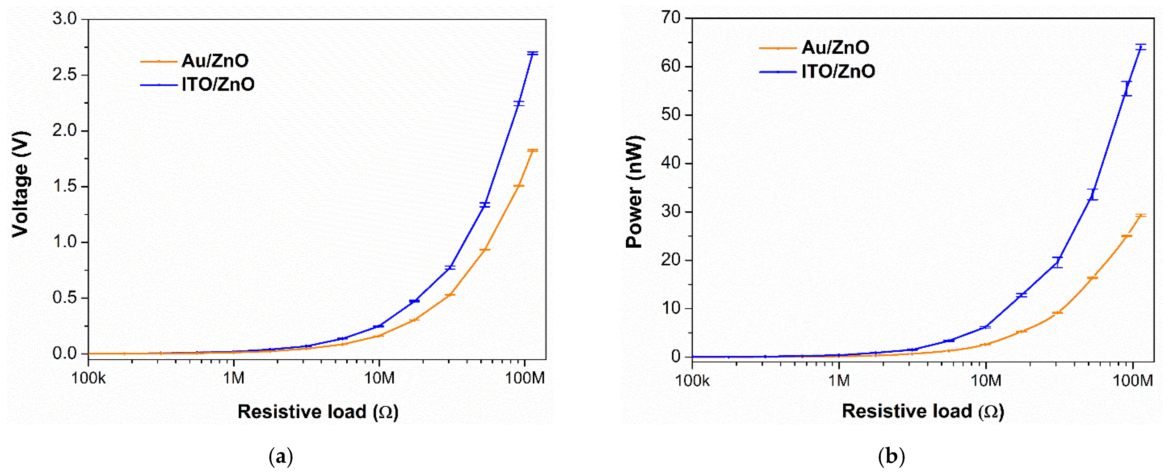
| Seed Layer Structure | Vpeak (V) | VRMS (max) (V) | Isc (RMS) (nA) | Pav (max) (nW) | W (nJ) | Ropt (MΩ) |
|---|---|---|---|---|---|---|
| Au/ZnO | 3.9 | 1.8 | 15 | 29 | 5.8 | >100 |
| ITO/ZnO | 6.8 | 2.7 | 28 | 64 | 12.8 | >100 |
| Substrate | Seed Layer Structure | Vpeak (V) | Mechanical Loading: Force (N) | Device Dimensions (cm2) | Ref. |
|---|---|---|---|---|---|
| Silicon | Au/ZnO | 0.27 | 3 | 1.2 | [11] |
| PDMS | Au/ZnO | 9.1 | 13 | 1.2 | [17] |
| PDMS | Au/ZnO | 2.03 | N/A | 1 | [37] |
| PDMS | ITO/ZnO | 8 | N/A | 1.5 | [38] |
| PDMS | ITO/ZnO | 6.8 | 3 | 1.2 | This work |
Publisher’s Note: MDPI stays neutral with regard to jurisdictional claims in published maps and institutional affiliations. |
© 2021 by the authors. Licensee MDPI, Basel, Switzerland. This article is an open access article distributed under the terms and conditions of the Creative Commons Attribution (CC BY) license (https://creativecommons.org/licenses/by/4.0/).
Share and Cite
Slimani Tlemcani, T.; Justeau, C.; Nadaud, K.; Alquier, D.; Poulin-Vittrant, G. Fabrication of Piezoelectric ZnO Nanowires Energy Harvester on Flexible Substrate Coated with Various Seed Layer Structures. Nanomaterials 2021, 11, 1433. https://doi.org/10.3390/nano11061433
Slimani Tlemcani T, Justeau C, Nadaud K, Alquier D, Poulin-Vittrant G. Fabrication of Piezoelectric ZnO Nanowires Energy Harvester on Flexible Substrate Coated with Various Seed Layer Structures. Nanomaterials. 2021; 11(6):1433. https://doi.org/10.3390/nano11061433
Chicago/Turabian StyleSlimani Tlemcani, Taoufik, Camille Justeau, Kevin Nadaud, Daniel Alquier, and Guylaine Poulin-Vittrant. 2021. "Fabrication of Piezoelectric ZnO Nanowires Energy Harvester on Flexible Substrate Coated with Various Seed Layer Structures" Nanomaterials 11, no. 6: 1433. https://doi.org/10.3390/nano11061433