Article

Effect of Annealing Temperature on Spatial Atomic Layer Deposited Titanium Oxide and Its Application in Perovskite Solar Cells

1
School of Opto-electronic and Communication Engineering, Xiamen University of Technology, Xiamen 361024, China
2
School of Information Engineering, Jimei University, Xiamen 361021, China
3
Department of Materials Science and Engineering, Da-Yeh University, Changhua 51591, Taiwan
4
CAS Key Laboratory of Design a Assembly of Functional Nanostructures, and Fujian Provincial Key Laboratory of Nanomaterials, Fujian Institute of Research on the Structure of Matter, Chinese Academy of Sciences, Fuzhou 350002, China
5
Key Laboratory of Green Perovskites Application of Fujian Province Universities, Fujian Jiangxia University, Fuzhou 350108, China
6
Fujian Key Laboratory of Optoelectronic Technology and Devices, Xiamen University of Technology, Xiamen 361024, China
*
Author to whom correspondence should be addressed.
Nanomaterials 2020, 10(7), 1322; https://doi.org/10.3390/nano10071322
Submission received: 27 May 2020 / Revised: 2 July 2020 / Accepted: 3 July 2020 / Published: 5 July 2020

Abstract

:
In this study, spatial atomic layer deposition (sALD) is employed to prepare titanium dioxide (TiO2) thin films by using titanium tetraisopropoxide and water as metal and water precursors, respectively. The post-annealing temperature is varied to investigate its effect on the properties of the TiO2 films. The experimental results show that the sALD TiO2 has a similar deposition rate per cycle to other ALD processes using oxygen plasma or ozone oxidant, implying that the growth is limited by titanium tetraisopropoxide steric hindrance. The structure of the as-deposited sALD TiO2 films is amorphous and changes to polycrystalline anatase at the annealing temperature of 450 °C. All the sALD TiO2 films have a low absorption coefficient at the level of 10−3 cm−1 at wavelengths greater than 500 nm. The annealing temperatures of 550 °C are expected to have a high compactness, evaluated by the refractive index and x-ray photoelectron spectrometer measurements. Finally, the 550 °C-annealed sALD TiO2 film with a thickness of ~8 nm is applied to perovskite solar cells as a compact electron transport layer. The significantly enhanced open-circuit voltage and conversion efficiency demonstrate the great potential of the sALD TiO2 compact layer in perovskite solar cell applications.

1. Introduction

Among a wide variety of metal oxides, TiO2 is a promising material for many emerging applications, such as gas sensors [1,2], dye-sensitized solar cells [3,4], photocatalysis [5] and gate insulators in metal-oxide-semiconductor field-effect transistors [6]. The characteristics of TiO2 thin films prepared by sol-gel, chemical vapor deposition or sputtering have been extensively studied [7,8,9,10]. Fujishima et al. reviewed the properties of TiO2 prepared by various methods, the fundamentals of photocatalysts, as well as applications [11]. Carp et al. reviewed the photoinduced reactivity of TiO2 [12]. In recent years, atomic layer deposition (ALD) has received great attention due to its unique features, such as the ability to prepare highly conformal thin films on high-aspect ratio substrates and to control the film thickness on an atomic level [13,14]. The self-limiting surface reaction in ALD leads to a continuous pinhole-free film, which can be used to deposit different metals, metal oxides and nitrides at relatively low temperatures [15,16,17]. Due to the high density of ALD thin films, single-layer and multi-layer stacks of TiO2 by thermal- and plasma-assisted ALD have been used for packaging and moisture-proof purposes [18,19]. The ALD TiO2 is also expected to be a promising electron transport layer (ETL) of perovskite solar cells owing to its high compactness and ability to have excellent coverage on a transparent conductive layer [20,21,22,23]. ALD TiO2 films can be deposited by using different titanium precursors, such as TiCl4 [24], TiI4 [25], tetra-dimethyl-amino titanium [26], titanium tetraisopropoxide (TTIP) [27], titanium ethoxide [28] and titanium methoxide [29]. Details for the preparation of TiO2 films based on these precursors are reviewed in ref. [30]. Among the various precursors, TTIP is cost-effective and has the highest vapor pressure, which makes it an interesting precursor for the ALD process development. For the metal precursors with a low vapor pressure, such as tetrakis(dimethylamido)titanium, the saturation of the surface chemical reaction can hardly be obtained unless by using a high bubbler temperature, high flow rate of the carrier gas and slow substrate moving speed. In comparison, by using a high vapor pressure precursor such as TTIP, a lower bubbler temperature and a faster substrate speed can be used.
Metal oxides often require an annealing process to improve the density of the film, and the crystal structure of the film is strongly affected by the annealing temperature. The existing research on TiO2 annealing is mostly based on sol-gel [8,31] or sputtering [32], where TiO2 is reported to have mainly three types of crystal phases, an anatase phase at below 600 °C, rutile phase at above 800 °C and brookite mesophase. The crystal phase of TiO2 also depends on the particle size, due to the interplay between the thermodynamic quantities, particularly the surface energy [33]. Although this is usually a concern for nanoparticles, nanocrystalline particles could be formed in the ALD films. Nabatame et al. [34] studied anatase TiO2 films fabricated by using ALD and postdeposition annealing, and discussed the flat band voltage change caused by the bottom interface dipole as well as how the dipole relates to oxygen introduced into the TiO2 layer during oxidation annealing. Few studies reported the effect of annealing on the properties of plasma or thermal ALD TiO2 films. Luka et al. studied the mechanism of the crystallization of thermal ALD TiO2 based on TiCl4/H2O annealed at 160–220 °C [35]. Matsui et al. reported that TiOx can act as either an electron or hole selective contact depending on the thermal or plasma ALD process and that its selectivity is strongly affected by post-annealing and the work function of the metal or transparent conducting oxide contact on top of the TiOx layer [36]. Won et al. investigated the effect of post-annealing in vacuum on the electrical properties and interfacial reaction in a thermal ALD TiO2/SiO2/Si system [37]. However, there are very limited studies on the annealing of TiO2 prepared by spatial ALD (sALD).
In this paper, TiO2 films are prepared by using sALD with TTIP and water precursors. The annealing temperature is varied, and its effect on the optical and crystalline properties of the films is investigated. Finally, the sALD TiO2 is applied to perovskite solar cells as a compact layer. The solar cell performance, such as the open circuit voltage (Voc), short circuit current density (Jsc), fill factor (FF) and conversion efficiency (η), is also discussed.

2. Materials and Methods
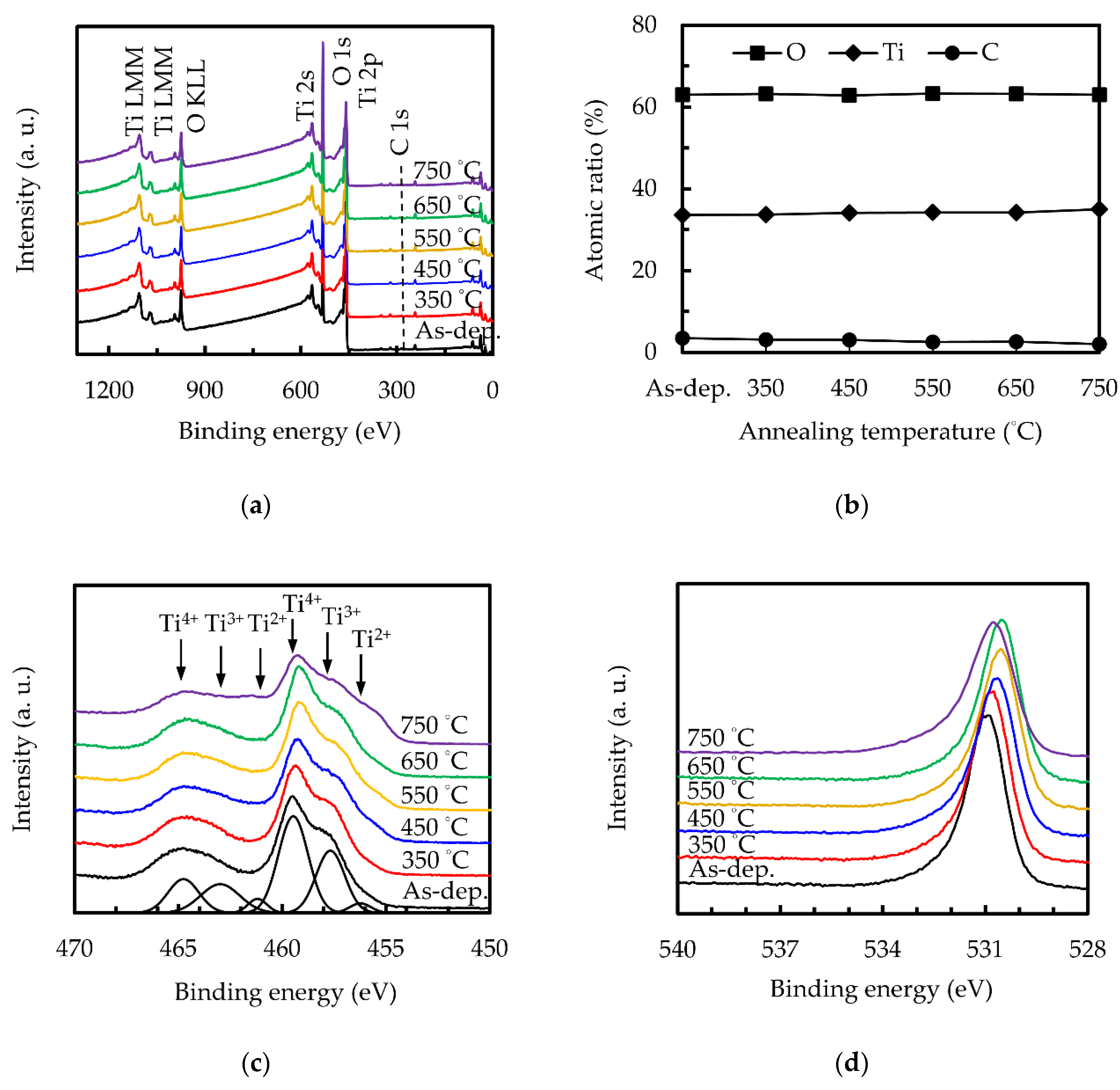
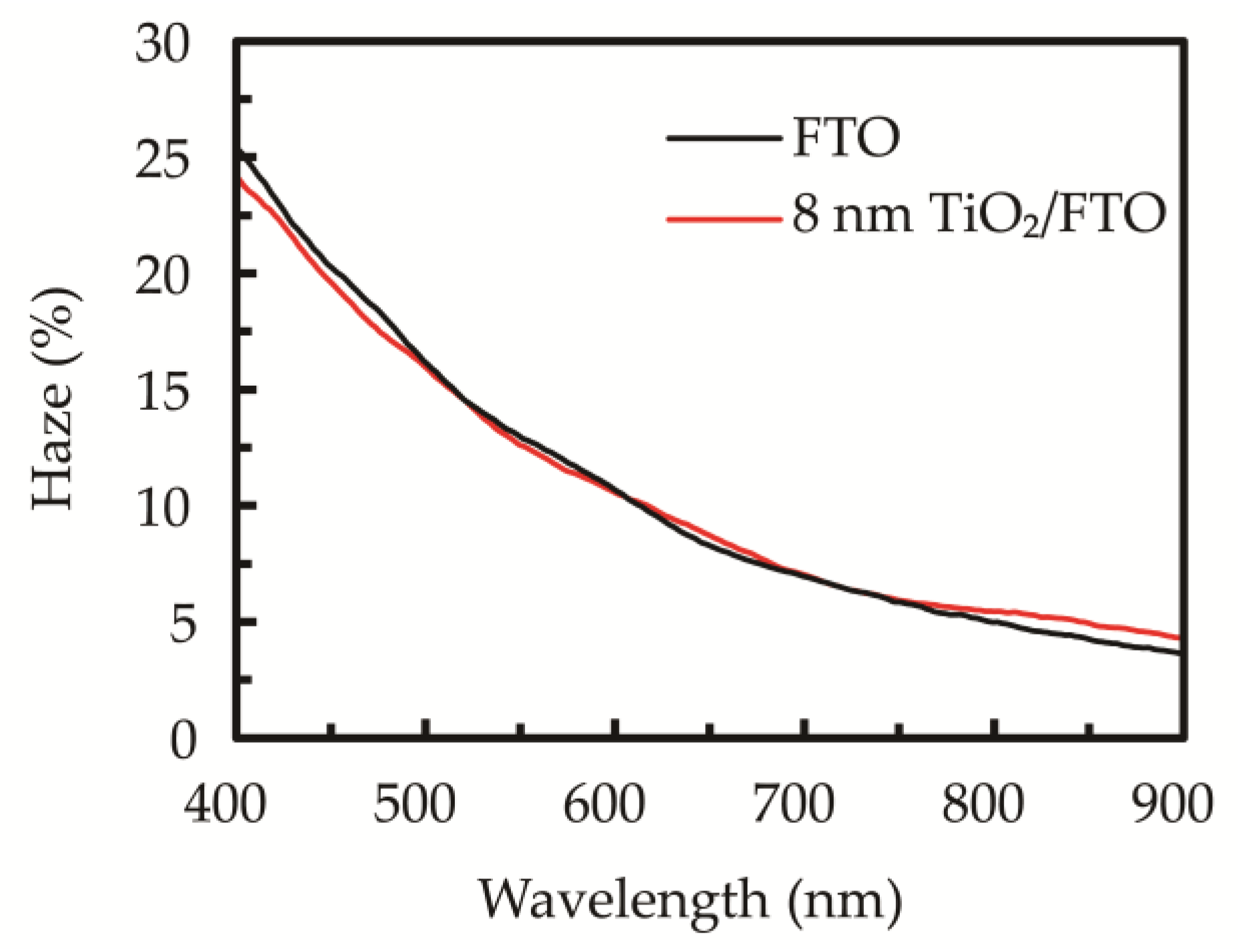
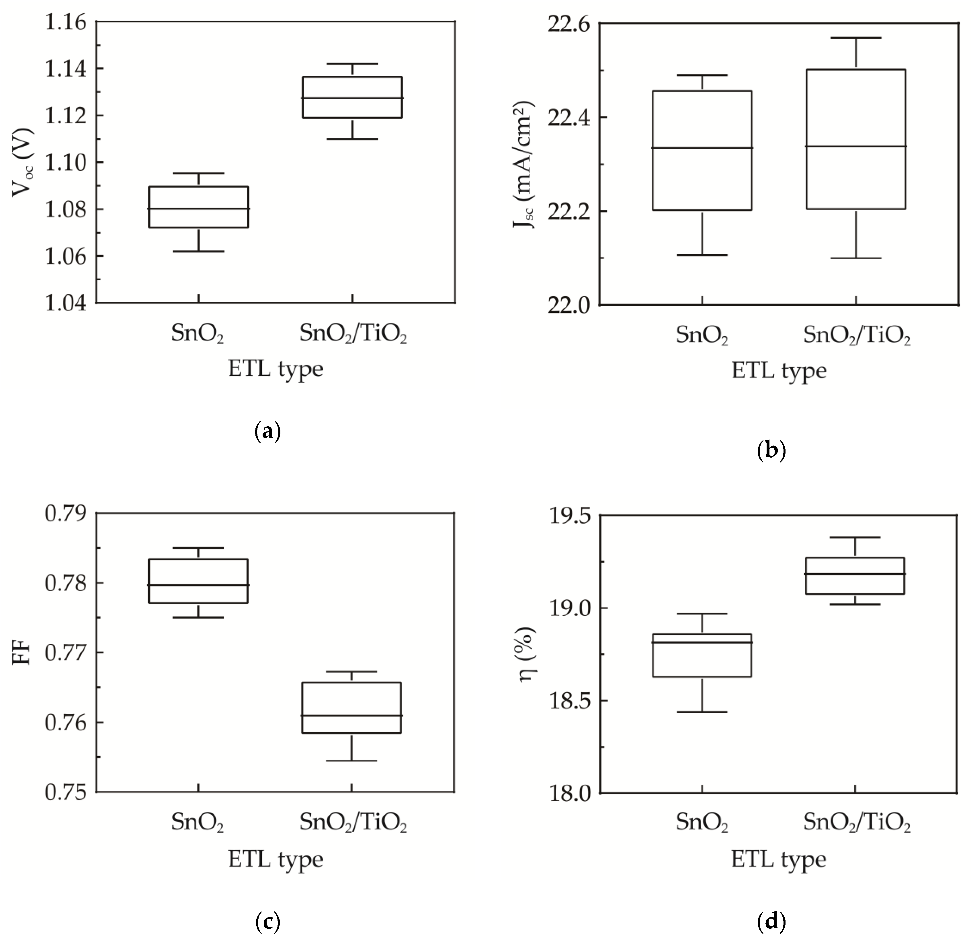
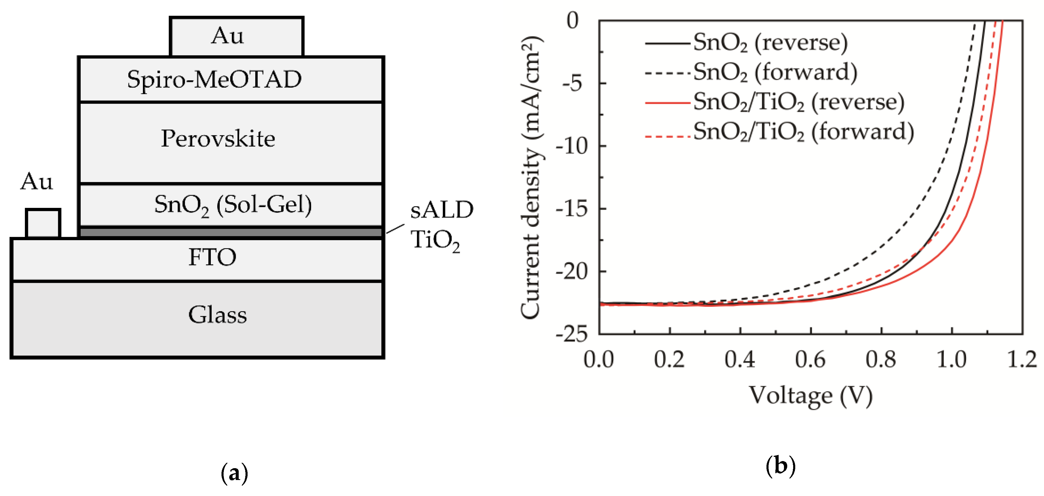
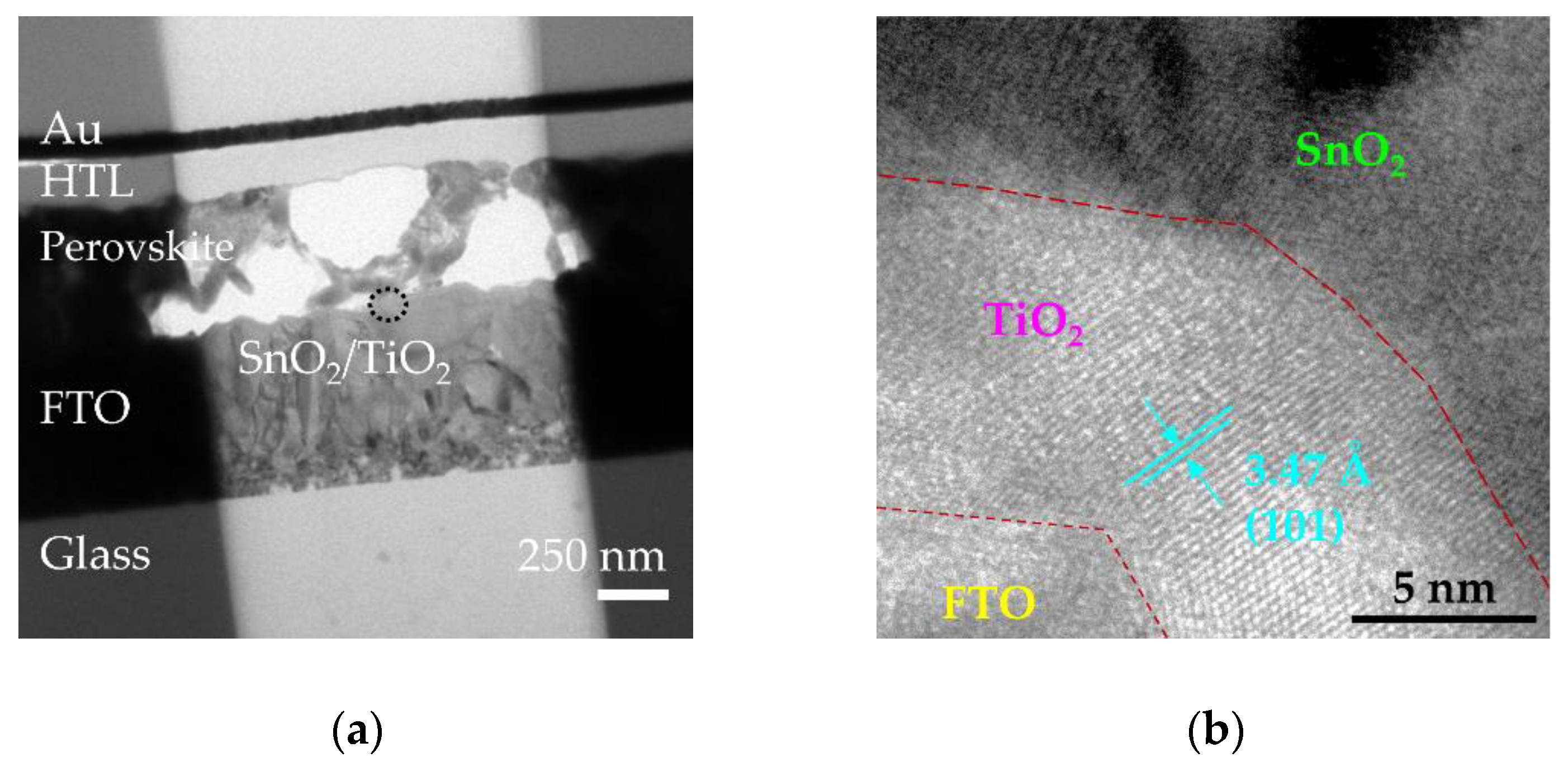
P-type 1–20 Ω-cm, CZ-type silicon (100) wafers and borosilicate glasses with a thickness of 0.2 mm were used as substrates. The glass substrates were ultrasonic-cleaned with propanol, alcohol and deionized water for 10 min each, and dried in nitrogen. The silicon wafers were cleaned using RCA standard procedures, followed by a dip in HF solution to remove natural oxide on the silicon surface, and finally they were dried with nitrogen. TiO2 thin films were prepared using a home-built sALD system (model Al2O3, Henghao, Taiwan) with TTIP (99.9999% purity, Aimou Yuan Scientific, Nanjing, China) and H2O as the titanium source and oxidant, respectively. The TTIP bubbler was placed in a gas cabinet equipped with a smoke detector. The vapor of the TTIP precursor was delivered through 1/4’ stainless steel tubing with VCR fittings to ensure safety. The reactor consisted of a substrate stage able to move back and forth and three precursor nozzles arranged in the order of H2O/TTIP/H2O. Each precursor nozzle was separated by a nitrogen curtain nozzle. The diameter of the nozzles was about 0.2 mm, and the gap between the injectors and substrate was 2 mm. The deposition area could be 15.6 cm × 15.6 cm. In this area, the error of the TiO2 film thickness was within 3%, evaluated from the nine-point measurement. The TTIP bubbler was heated to 70 °C to obtain a sufficiently high vapor pressure. Nitrogen (99.999% purity) was used as the carrier gas. The TTIP pipeline was heated to 75 °C to prevent vapor condensation. The temperature of the deionized water bubbler and delivery pipeline were kept to 25 and 30 °C, respectively. The substrate temperature was set to 110 °C. Nitrogen with flow rates of 400 and 2000 sccm were used as the carrier gas for TTIP and water, respectively, in order to take the precursor vapor out of the bubbler before it was diluted in 800 and 4000 sccm of nitrogen before injecting it into the substrate. A flow rate of 15,000 sccm was used for the nitrogen curtain. The detailed process parameters are listed in Table 1. After the film deposition, the samples were annealed in a furnace tube in nitrogen ambient at 350–750 °C for 30 min. The TiO2 films were deposited on the glass and silicon in order to investigate the effect of the annealing temperature on the optical and structural properties of the films. The thickness and refractive index of the films were determined using an ellipsometer (M-2000, J. A. Woollam Co., Inc., Lincoln, NE, USA). The crystalline structure of the films was characterized using a grazing incidence X-ray diffractometer (TTRAXIII, Rigaku Co., Tokyo, Japan) with an incident angle of 0.5° over the 2θ range of 20–60° using CuKα radiation (λ = 1.5405 Å), 45 kV cathode voltage and 40 mA cathode current. The chemical state and composition of the films were obtained by an X-ray photoelectron spectrometer (XPS, ESCALAB 250Xi, Thermo Fisher Scientific Co., San Jose, CA, USA) with an Al-Ka monochromatic source. The transmittance and reflectance of the samples were measured by a UV-visible spectrometer (MFS-630, Hong-Ming Technology, New Taipei, Taiwan).
For the perovskite solar cell fabrication, 2 cm × 2 cm fluorine-doped tin oxide (FTO) glass substrates were cleaned with a detergent solution, deionized water, acetone and anhydrous ethanol for 10 min each. The substrates were further cleaned with UV ozone for 30 min, followed by the deposition of the sALD TiO2 layer with a thickness of ~8 nm. A ~50 nm, the SnO2 layer was then deposited on the sALD TiO2 by spin-coating a diluted SnO2 nanoparticle paste (2.7% in ultra-pure water) (Alfa Aesar, Shanghai, China) at 3000 rpm for 45 s, and dried at 150 °C for 30 min and sintered at 550 °C for 30 min in a muffle furnace (Michem instruments Co., Beijing, China). Formamidinium iodide (TCl America, Portland, OR, USA), methylammonium bromide (Aladdin, Shanghai, China), lead bromide (Sigma-Aldrich, St. Louis, MO, USA) and lead iodide (Alfa Aesar, Shanghai, China) were dissolved in a mixed solvent of N,N-dimethylformamide (DMF, Aladdin, Shanghai, China) and dimethyl sulfoxide (DMSO, Aladdin, Shanghai, China) (4:1 volume ratio) by a molar ratio of 1:1.15:0.2:0.2. Then, CsI (Sigma-Aldrich, St. Louis, MO, USA) previously dissolved as 1.5 mol stock solution in DMSO was added to the DMF/DMSO solution to achieve the Cs0.1(FA0.83MA0.17)0.9Pb(I0.83Br0.17)3 perovskite precursor solution, which was spin-coated on the SnO2 in a two-step process at 1000 rpm for 10 s and 6000 rpm for 25 s in a nitrogen glove box. Chlorobenzene (Aladdin, Shanghai, China) of 110 μL was dropped on the spinning substrate at 5 s before the second process finished. The substrates were then annealed at 100 °C for 1 h on a hotplate in order to obtain crystalline 3D perovskite films. After the substrates were cooled to room temperature, 50 μL of Spiro-MeOTAD (Lumtec, New Taipei, Taiwan) was spin-coated on the perovskite layers at 4000 rpm for 30 s. The devices were finalized by evaporating Au on the top of the Spiro-MeOTAD layer. The active area of perovskite solar cells was 0.5 cm × 0.5 cm. The cross-sectional images of the perovskite solar cells were obtained using a transmission electron microscope (TEM, CM200, Philips, Hillsboro, OR, USA). The photovoltaic performance was measured using a digital source meter (Model 2420, Keithley Instruments Inc., Cleveland, OH, USA) under an illumination of 100 mW/cm2 produced by a solar simulator at AM 1.5 G (Newport Oriel, Irvine, CA, USA). The light intensity was calibrated with a Si reference cell (Newport Corporation, Irvine, CA, USA) before the measurement. The J-V characteristics of PSCs were measured in forward (−0.1 to 1.2 V) and reverse (1.2 to −0.1 V) scan modes at a scan rate of 200 mV/s within a step of 20 mV.

3. Results

Figure 1a shows a schematic diagram of the growth mechanism of sALD TiO2 films with TTIP/H2O precursors. On some substrates such as glass, the surface naturally carries hydroxyl groups. Otherwise, the surface will be hydroxylated when exposed to H2O for the first time. Excess precursor molecules are exhausted, and then the substrate moves to the TTIP precursor zone. Surface ligand exchange occurs between the hydroxyl group and TTIP, followed by the release of gaseous (C3H7)OH molecules. The chemical reaction can be described as [38]:
S–OH* + Ti(C3H7O)4 → S–O–Ti(C3H7O)3* + (C3H7)OH
where S represents the substrate surface. Since TTIP only reacts with the surface hydroxyl groups but not with itself, a single layer of Ti(C3H7O)3 is formed. The substrate then moves to the H2O precursor area, resulting in the following reaction:
Si–O–Ti(C3H7O)* + H2O → S–O–Ti(OH)* + (C3H7)OH
A monolayer of TiO2 is deposited after TTIP and H2O exposure. It is worth noting that one sALD cycle takes 3 s per cycle, while vacuum-based thermal or plasma ALD takes more than 1 min, including precursor injection, purge and exhaust. Figure 1b shows the thickness of the SALD TiO2 films (1000 cycles) as a function of the annealing temperature. The thickness of the as-deposited TiO2 film is 68.3 nm, which corresponds to a growth per cycle (GPC) of 0.68 Å/cycle. This value is similar to the values of vacuum ALD using O2-plamsa [39], ozone [40] or H2O oxidant [41], suggesting that the growth is mainly limited by the steric hindrance of TTIP instead of the growth sites created by the oxidizing agent. After annealing at 350 °C, the film thickness decreased to 60 nm, and a further increase in the annealing temperature caused a slight decrease in thickness. The obvious thickness drops at 350 °C may be due to the release of unreacted precursors in the film, which is consistent with the decomposition temperature of TTIP at 275 °C [42]. The slight decrease in thickness at higher temperatures is caused by the densification of the films.
Figure 2a shows the refractive index spectra of sALD TiO2 films at different annealing temperatures. For a comparison between different samples, we choose the refractive index with a 630 nm wavelength, as shown in Figure 2b, which is usually used for solar cell applications as it corresponds to the highest intensity of the solar spectrum. The refractive index of the film before annealing is 2.3 and seems to reach the maximal value of 2.4 as the annealing temperature reaches 550–750 °C. It is reported that the density of TiO2 films generally increases with the refractive index [43]. The films annealed at 550–750 °C have the highest refractive index, which is similar to those of high-quality PEALD TiO2 films with a corresponding film density of 3.8 g/cm3 [43]. In comparison, the sol-gel spin-coated TiO2 films have refractive indices typically under 2.2 [44,45], corresponding to a density of 2.95 g/cm3.
Figure 3a shows the transmittance and reflectance spectra of the sALD TiO2 film at different annealing temperatures. The trend of the transmittance curves is opposite to that of the reflectance curves. This indicates that the change between the transmittance is mainly due to the reflectance, which is caused by the differences in the refractive index and thickness after annealing. Figure 3b shows the average transmittance, average reflectance and band gap for the sALD TiO2 films. The average transmittance and reflectance of the films range from 64.9–67.9% and from 30.5–33.8%, respectively. To further eliminate the disturbance caused by the sample thickness and reflection, we calculated the absorption coefficient of the films, which can be written as:
α ( λ ) = 1 d ln [ T ( λ ) 1 R 2 ( λ ) ]
where α is the absorption coefficient, T is the transmittance, R is the reflectance, λ is the wavelength and d is the film thickness. The magnitude of the absorption coefficient does not change significantly with the annealing temperature, and it stays at a low level of 103 cm−1 at wavelengths greater than 500 nm for all the samples. However, the absorption coefficient of these sALD TiO2 films at shorter wavelengths (< 500 nm) is relatively higher, which is to say at the level of 104 cm−1, suggesting that the thickness of the films should still not be too thick for their use as a window layer of solar cells. The band gap of the films was obtained using the Tauc plot method [46]:
(αhv)n = A (hvEg)
where Eg is the band gap, hv is the photon energy, A is a material constant and the exponent n characterizes the nature of the electron transition. For the indirect band gap n = 2, the value of the gap is obtained from the x-intercept of the extrapolated linear part of the graph (αhv)1/2 versus the photon energy, which is widely used in the literature for TiO2 [10,47]. The as-deposited film had the highest band gap, at 3.25 eV. When the annealing temperature increases from 350 to 750 °C, the band gap decreases from 3.23 to 3.18 eV. The band gap before annealing is consistent with that of amorphous TiO2. The decrease in the band gap with an increasing annealing temperature implies the structural change of the films. The samples annealed at below 750 °C have band gap values similar to anatase TiO2 (~3.2–3.25 eV), while the 750 °C-annealed sample shows a reduced band gap similar to rutile TiO2 [48].
To confirm the crystalline structure, the X-ray diffraction patterns of the sALD TiO2 films with different annealing temperatures are shown in Figure 4a. The peaks at 2θ = 25.3°, 36.9°, 37.8°, 38.6°, 48.1°, 53.9°and 55.1° correspond to (101), (103), (004), (112), (200), (105) and (211) anatase phases (JCPSD card #83-2243). The sample before annealing did not have any observable peaks. This is in good agreement with other studies using thermal ALD, showing that deposition below 200 °C results in amorphous TiO2 [49,50,51]. The film annealed at 350 °C seems to have a very weak peak at 25.3°, but it was difficult to distinguish from the background. The film structure changes from amorphous to polycrystalline anatase at 450 °C. When the annealing temperature increases to 750 °C, no other phases such as rutile (main peak at 2θ = 27°) are presented, indicating that the film maintains the polycrystalline anatase phase in a wide temperature range. The previously mentioned low band gap of the 750 °C-annealed sample is therefore not attributed to the formation of the rutile phase. Another possible reason for the low band gap is related to the sub-bandgap absorption caused by high temperature-generated defects, leading to localized states under the conduction band minimum and a shift of the absorption edge towards long wavelengths. Figure 4b shows the full width at half maximum (FWHM) of the diffraction peaks as a function of the annealing temperature. It can be seen that the FWHM of the (100) and (200) peaks do not change significantly. The FWHM of the (211) peak rises with an increasing annealing temperature, while the FWHM of the (105) peak decreases, implying that annealing temperature causes the (211) anatase phase to be gradually replaced by the (105) phase.
Figure 5a shows the XPS spectra of sALD TiO2 thin films at different annealing temperatures. The Ti, O and C atomic ratios obtained from the XPS spectra are shown in Figure 5b, showing that all the films are oxygen-deficient with O/Ti ratios ranging from 1.87 to 1.79. The C atomic ratio decreases with an increasing annealing temperature. Figure 5c shows a high resolution of the Ti 2p peaks. All subsequent analyses are only based on the Ti 2p3/2 spin-orbit coupling state, but both the 1/2 and 3/2 states are fitted because the split is only about 5.7 eV, which leads to the overlap of Ti3/24+ and Ti1/22+. Compared with the 3/2 state, the area ratio of the 1/2 state is 0.43 ± 0.03. One can see that Ti 2p3/2 has three different oxidation states, which correspond to Ti4+ of 459 ± 0.2 eV, Ti3+ of 457.2 ± 0.2 eV and Ti2+ of 455.9 ± 0.2 eV, respectively [52,53]. It can be seen that the samples with an annealing temperature below 650 °C have similar results and that the proportion of Ti4+ increases slightly with an increasing annealing temperature, reaching the maximum at 550 and 650 °C. However, when the annealing temperature further increases to 750 °C, the composition of Ti3+ and especially Ti2+ increases significantly. In the O 1s spectrum, as shown in Figure 5d, the main peak shifts from 531.33 eV toward a lower energy. In the literature, the binding energy of 531.33 eV is usually related to hydroxyl groups, carbonate-like substances or other carbon-related impurities, or to oxygen-deficient titanium dioxide (e.g., TiOx, where 1.35 < x < 1.65) [54]. The first two explanations may be reasonable on the surface in the as-deposited state because it may have hydroxyl or carbon impurities that are adsorbed from the air or that remain in the structure as residues of incompletely reacted ALD precursors. The shift of the peak towards 530.2 eV corresponding to O2− in TiO2 reveals the reduction of incompletely reacted ALD precursors and hence the densification after receiving the annealing treatment. The binding energy increases for the 750 °C-annealing can be explained by the increase in oxygen vacancies, arising from the desorption of oxygen.
From the above results, the 550 °C-annealed sALD TiO2 film having the highest compactness is considered for use as a compact layer of perovskite solar cells. The haze spectra of the FTO substrate without and with the 8-nm sALD TiO2 film is shown in Figure 6. The haze, defined as the percentage of light that is scattered at more than 2.5° from the incident light direction, is used as an indicator of the light diffusion. It is seen that the haze of the chemical-etched FTO is 25% at 400 nm, and it decreases to about 5% at 900 nm. The sALD TiO2 film on FTO does not significantly change the haze spectrum due to the high conformality and very thin thickness. The low degree of difference between the two spectra implies that the thin TiO2 deposition does not significantly change the optical property.
Figure 7 shows the photovoltaic performance of the perovskite solar cells without and with the 8-nm sALD TiO2 compact layer measured in reverse scan. The error bars indicate the range of the data from ten cells fabricated under identical conditions. It can be seen that the cell with the sALD TiO2 compact layer shows a significant increase in Voc (Figure 7a). The lower Voc of the sol-gel SnO2 ETL alone implies that some of photo-generated holes are likely to pass through the ETL to recombine with electrons. This leads to an increase in the leakage current of the device. According to the following equation:
V o c = k T q ln ( I s c I 0 + 1 )
where kT/q is the thermal voltage, Isc is the short-circuit current and I0 is the leakage current. Therefore, the hole-electron recombination at the FTO/ETL interface reduces the Voc. The sALD TiO2 used as a compact layer leads to enhanced hole blocking, a reduced leakage current and eventually an improved Voc, even at such a small thickness. The Jsc is not much influenced as shown in Figure 7b due to the similar refractive indices of TiO2 and SnO2, and the very thin TiO2 thickness. The amount of incident light is not much affected by the insertion of the sALD TiO2 layer. The slight decrease in FF as shown in Figure 7c could be explained by the increase in series resistance caused by the addition of the sALD TiO2 layer, and therefore it is important to keep the thickness of TiO2 as thin as possible. Overall, the conversion efficiency is significantly improved due to the Voc enhancement (Figure 7d). In the literature, most of the solution-based single-layer or double-layer ETLs give a Voc of 1.05–1.11 V [55,56,57,58], while the plasma-enhanced ALD or thermal ALD ETLs generally show a Voc of 1.09–1.11 V [59,60,61]. The sALD SnO2/TiO2 ETL in this study leads to an improved Voc. Furthermore, while the sALD and traditional vacuum-type ALDs have insignificantly different GPC values (~0.7 Å/cycle), it costs 3 s for one sALD cycle and at least 60 s in the case of the plasma or thermal ALD. For an 8-nm thickness of TiO2, sALD needs about 6 min to finish the deposition, whereas other ALDs require about 70 min. In this study, a high deposition rate sALD is used for preparing the very thin TiO2 compact layer. Although it is noted that the crystallinity of the 8-nm sALD TiO2 may not behave exactly as the 60-nm layer previously used for film characterization, the thin TiO2 compact layer leads to an improved Voc and conversion efficiency. The sALD is thus more advantageous in the application of perovskite solar cells.
Figure 8a shows the device structure, where the sALD TiO2 is added and inserted between the FTO and sol-gel SnO2 ETL in order to enhance hole blocking. The thicknesses of the FTO, sALD TiO2, sol-gel SnO2, perovskite layer, Spiro-MeOTAD and Au are about 600, 8, 50, 450, 150 and 65 nm, respectively. The corresponding cross-sectional TEM image for the device is shown in Figure 9a, and the high-resolution image at the interface region of FTO/sALD TiO2/sol-gel SnO2 is observed in Figure 9b, evidencing the very smooth interface and uniform (or conformal) TiO2 layer covering on FTO. The main lattice structure in the sALD TiO2 is evaluated to be 3.47 Å, which is indexed to the TiO2 (101) phase. Figure 8b compares the J-V curves for the highest efficiency perovskite solar cells without and with the sALD TiO2 compact layer. The corresponding external photovoltaic parameters are listed in Table 2. To quantify the magnitude of the hysteretic effect, the hysteresis index (HI), defined as HI = (Poc-scPsc-oc)/(Poc-sc + Psc-oc), is used, where P o c s c = s c o c J R ( V ) Θ ( J R ) d V and P s c o c = o c s c J F ( V ) ϑ ( J F ) d V are the values of the integral power output in the reverse and forward directions, respectively [62]. Θ is the Heaviside step function. It is found that the HI decreases by nearly 50% with the addition of the sALD TiO2 compact layer. Furthermore, the conversion efficiency of the perovskite solar cells was measured after fabrication and after one, three, five and seven days. The cells were stored in a nitrogen box. The cell efficiency measured at one day after fabrication was the highest, and the data are shown in Figure 8b. The cell efficiency degraded by about 5% when measured at seven days after fabrication. To further improve the stability, perovskite halides doped with Ni or Co might be a possible option, as suggested in ref. [63]. It is concluded that the sALD TiO2 with a high compactness, precise thickness control, high deposition rate and good step coverage demonstrates great potential for the applications of perovskite solar cells.

4. Conclusions

The TiO2 thin films are prepared using high growth rate sALD using TTIP and H2O precursors with different post-annealing temperatures. The 550–750 °C-annealed films have a refractive index of 2.4, close to the values of high-quality PEALD films and significantly higher than that obtained by the sol-gel spin-coating technique. All the TiO2 films have a low absorption coefficient at the 10−3 cm−1 level for wavelengths greater than 500 nm. The 550 and 650 °C-annealed TiO2 shows the highest Ti4+ proportion, while further increasing the annealing temperature to 750 °C leads to an increase in oxygen vacancies. Finally, the 550 °C-annealed sALD TiO2 compact layer with a very thin thickness of ~8 nm shows a significant improvement in Voc, demonstrating the great potential of sALD films for perovskite solar cell applications.

Author Contributions

Conceptualization, C.-H.H. and S.-Y.L.; methodology, K.-T.C., P.-H.H., Z.-B.S. and Z.-R.C.; formal analysis, C.-H.H., W.-Y.W., X.-Y.Z., C.W., L.-S.L., P.G. and Y.Q.; writing—original draft preparation, C.-H.H. and K.-T.C.; writing—review and editing, C.-H.H. and S.-Y.L.; funding acquisition, C.-H.H., S.-Y.L., P.G. and W.-Z.Z. All authors have read and agreed to the published version of the manuscript.

Funding

This work is supported by the scientific research projects of Xiamen University of Technology (grant nos. 0105-50419030, 30319003 and YKJ19001R). This work is also sponsored by the science and technology project of Xiamen (No. 3502Z20183054) and the Science and Technology Program of the Educational Office of Fujian Province (No. JT180432). P. Gao knowledge ‘the National Natural Science Foundation of China (Grant No. 21975260) and the Recruitment Program of Global Experts (1000 Talents Plan) of China’.

Conflicts of Interest

The authors declare no conflict of interest.

References

  1. Liu, H.; Shen, W.; Chen, X. A room temperature operated ammonia gas sensor based on Ag-decorated TiO2 quantum dot clusters. RSC Adv. 2019, 9, 24519–24526. [Google Scholar] [CrossRef] [Green Version]
  2. Li, Z.; Yao, Z.; Haidry, A.A.; Plecenik, T.; Xie, L.; Sun, L.; Fatima, Q. Resistive-type hydrogen gas sensor based on TiO2: A review. Int. J. Hydrog. Energy 2018, 43, 21114–21132. [Google Scholar] [CrossRef]
  3. Chen, W.-C.; Yeh, M.-H.; Lin, L.-Y.; Vittal, R.; Ho, K.-C. Double-Wall TiO2 Nanotubes for Dye-Sensitized Solar Cells: A Study of Growth Mechanism. ACS Sustain. Chem. Eng. 2018, 6, 3907–3915. [Google Scholar] [CrossRef]
  4. Son, Y.J.; Kang, J.S.; Yoon, J.; Kim, J.; Jeong, J.; Kang, J.; Lee, M.J.; Park, H.S.; Sung, Y.-E. Influence of TiO2 Particle Size on Dye-Sensitized Solar Cells Employing an Organic Sensitizer and a Cobalt(III/II) Redox Electrolyte. J. Phys. Chem. C 2018, 122, 7051–7060. [Google Scholar] [CrossRef]
  5. Guo, Q.; Zhou, C.; Ma, Z.; Yang, X. Fundamentals of TiO2 Photocatalysis: Concepts, Mechanisms, and Challenges. Adv. Mater. 2019, 31, 1901997. [Google Scholar] [CrossRef]
  6. Lin, Y.-S.; Lu, C.-C. Improved AlGaN/GaN Metal–Oxide– Semiconductor High-Electron Mobility Transistors With TiO2 Gate Dielectric Annealed in Nitrogen. IEEE Trans. Electron Devices 2018, 65, 783–787. [Google Scholar] [CrossRef]
  7. Ullattil, S.G.; Periyat, P. Sol-Gel Synthesis of Titanium Dioxide. In Sol-Gel Materials for Energy, Environment and Electronic Applications; Pillai, S.C., Hehir, S., Eds.; Advances in Sol-Gel Derived Materials and Technologies; Springer International Publishing: Cham, Switzerland, 2017; pp. 271–283. ISBN 978-3-319-50142-0. [Google Scholar]
  8. Kang, S.; Mauchauffé, R.; You, Y.S.; Moon, S.Y. Insights into the Role of Plasma in Atmospheric Pressure Chemical Vapor Deposition of Titanium Dioxide Thin Films. Sci. Rep. 2018, 8, 16684. [Google Scholar] [CrossRef] [Green Version]
  9. Li, D.; Elisabeth, S.; Granier, A.; Carette, M.; Goullet, A.; Landesman, J.-P. Structural and Optical Properties of PECVD TiO2 -SiO2 Mixed Oxide Films for Optical Applications: Structural and Optical Properties of PECVD TiO2 -SiO2 …. Plasma Process. Polym. 2016, 13, 918–928. [Google Scholar] [CrossRef]
  10. Nezar, S.; Saoula, N.; Sali, S.; Faiz, M.; Mekki, M.; Laoufi, N.A.; Tabet, N. Properties of TiO2 thin films deposited by rf reactive magnetron sputtering on biased substrates. Appl. Surf. Sci. 2017, 395, 172–179. [Google Scholar] [CrossRef]
  11. Fujishima, A.; Zhang, X.; Tryk, D. TiO2 photocatalysis and related surface phenomena. Surf. Sci. Rep. 2008, 63, 515–582. [Google Scholar] [CrossRef]
  12. Carp, O. Photoinduced reactivity of titanium dioxide. Progress Solid State Chem. 2004, 32, 33–177. [Google Scholar] [CrossRef]
  13. Cremers, V.; Puurunen, R.L.; Dendooven, J. Conformality in atomic layer deposition: Current status overview of analysis and modelling. Appl. Phys. Rev. 2019, 6, 021302. [Google Scholar] [CrossRef] [Green Version]
  14. Johnson, R.W.; Hultqvist, A.; Bent, S.F. A brief review of atomic layer deposition: From fundamentals to applications. Mater. Today 2014, 17, 236–246. [Google Scholar] [CrossRef]
  15. Sheng, J.; Lee, J.-H.; Choi, W.-H.; Hong, T.; Kim, M.; Park, J.-S. Review Article: Atomic layer deposition for oxide semiconductor thin film transistors: Advances in research and development. J. Vac. Sci. Technol. A 2018, 36, 060801. [Google Scholar] [CrossRef] [Green Version]
  16. Kaloyeros, A.E.; Jové, F.A.; Goff, J.; Arkles, B. Review—Silicon Nitride and Silicon Nitride-Rich Thin Film Technologies: Trends in Deposition Techniques and Related Applications. ECS J. Solid State Sci. Technol. 2017, 6, P691–P714. [Google Scholar] [CrossRef]
  17. Hagen, D.J.; Pemble, M.E.; Karppinen, M. Atomic layer deposition of metals: Precursors and film growth. Appl. Phys. Rev. 2019, 6, 041309. [Google Scholar] [CrossRef]
  18. Lv, Y.; Xu, P.; Ren, G.; Chen, F.; Nan, H.; Liu, R.; Wang, D.; Tan, X.; Liu, X.; Zhang, H.; et al. Low-Temperature Atomic Layer Deposition of Metal Oxide Layers for Perovskite Solar Cells with High Efficiency and Stability under Harsh Environmental Conditions. ACS Appl. Mater. Interfaces 2018, 10, 23928–23937. [Google Scholar] [CrossRef]
  19. Dias, V.; Maciel, H.; Fraga, M.; Lobo, A.; Pessoa, R.; Marciano, F. Atomic Layer Deposited TiO2 and Al2O3 Thin Films as Coatings for Aluminum Food Packaging Application. Materials 2019, 12, 682. [Google Scholar] [CrossRef] [Green Version]
  20. Kim, I.S.; Haasch, R.T.; Cao, D.H.; Farha, O.K.; Hupp, J.T.; Kanatzidis, M.G.; Martinson, A.B.F. Amorphous TiO2 Compact Layers via ALD for Planar Halide Perovskite Photovoltaics. ACS Appl. Mater. Interfaces 2016, 8, 24310–24314. [Google Scholar] [CrossRef]
  21. Zardetto, V.; Di Giacomo, F.; Lucarelli, G.; Kessels, W.M.M.; Brown, T.M.; Creatore, M. Plasma-assisted atomic layer deposition of TiO2 compact layers for flexible mesostructured perovskite solar cells. Sol. Energy 2017, 150, 447–453. [Google Scholar] [CrossRef]
  22. Chandiran, A.K.; Yella, A.; Mayer, M.T.; Gao, P.; Nazeeruddin, M.K.; Grätzel, M. Sub-Nanometer Conformal TiO2 Blocking Layer for High Efficiency Solid-State Perovskite Absorber Solar Cells. Adv. Mater. 2014, 26, 4309–4312. [Google Scholar] [CrossRef] [PubMed]
  23. Gao, P.; Grätzel, M.; Nazeeruddin, M.K. Organohalide lead perovskites for photovoltaic applications. Energy Environ. Sci. 2014, 7, 2448–2463. [Google Scholar] [CrossRef]
  24. Aarik, J.; Aidla, A.; Mändar, H.; Uustare, T. Atomic layer deposition of titanium dioxide from TiCl4 and H2O: Investigation of growth mechanism. Appl. Surf. Sci. 2001, 172, 148–158. [Google Scholar] [CrossRef]
  25. Aarik, J.; Aidla, A.; Uustare, T.; Kukli, K.; Sammelselg, V.; Ritala, M.; Leskelä, M. Atomic layer deposition of TiO2 thin films from TiI4 and H2O. Appl. Surf. Sci. 2002, 193, 277–286. [Google Scholar] [CrossRef]
  26. Tao, Q.; Overhage, K.; Jursich, G.; Takoudis, C. On the initial growth of atomic layer deposited TiO2 films on silicon and copper surfaces. Thin Solid Films 2012, 520, 6752–6756. [Google Scholar] [CrossRef]
  27. Aarik, J.; Aidla, A.; Uustare, T.; Ritala, M.; Leskelä, M. Titanium isopropoxide as a precursor for atomic layer deposition: Characterization of titanium dioxide growth process. Appl. Surf. Sci. 2000, 161, 385–395. [Google Scholar] [CrossRef]
  28. Aarik, J.; Karlis, J.; Mändar, H.; Uustare, T.; Sammelselg, V. Influence of structure development on atomic layer deposition of TiO2 thin films. Appl. Surf. Sci. 2001, 181, 339–348. [Google Scholar] [CrossRef]
  29. Alekhin, A.P.; Gudkova, S.A.; Markeev, A.M.; Mitiaev, A.S.; Sigarev, A.A.; Toknova, V.F. Structural properties of the titanium dioxide thin films grown by atomic layer deposition at various numbers of reaction cycles. Appl. Surf. Sci. 2010, 257, 186–191. [Google Scholar] [CrossRef]
  30. Niemelä, J.-P.; Marin, G.; Karppinen, M. Titanium dioxide thin films by atomic layer deposition: A review. Semicond. Sci. Technol. 2017, 32, 093005. [Google Scholar] [CrossRef]
  31. Bakri, A.S.; Sahdan, M.Z.; Adriyanto, F.; Raship, N.A.; Said, N.D.M.; Abdullah, S.A.; Rahim, M.S. Effect of annealing temperature of titanium dioxide thin films on structural and electrical properties. AIP Conf. Proc. 2017, 1788, 030030. [Google Scholar]
  32. Hadjoub, I.; Touam, T.; Chelouche, A.; Atoui, M.; Solard, J.; Chakaroun, M.; Fischer, A.; Boudrioua, A.; Peng, L.-H. Post-deposition annealing effect on RF-sputtered TiO2 thin-film properties for photonic applications. Appl. Phys. A 2016, 122, 78. [Google Scholar] [CrossRef]
  33. Zhang, H.; Banfield, J.F. Understanding Polymorphic Phase Transformation Behavior during Growth of Nanocrystalline Aggregates: Insights from TiO2. J. Phys. Chem. B 2000, 104, 3481–3487. [Google Scholar] [CrossRef]
  34. Nabatame, T.; Ohi, A.; Chikyo, T.; Kimura, M.; Yamada, H.; Ohishi, T. Electrical properties of anatase TiO2 films by atomic layer deposition and low annealing temperature. J. Vac. Sci. Technol. B Nanotechnol. Microelectron. Mater. Process. Meas. Phenom. 2014, 32, 03D121. [Google Scholar] [CrossRef]
  35. Luka, G.; Witkowski, B.S.; Wachnicki, L.; Andrzejczuk, M.; Lewandowska, M.; Godlewski, M. Kinetics of anatase phase formation in TiO2 films during atomic layer deposition and post-deposition annealing. CrystEngComm 2013, 15, 9949. [Google Scholar] [CrossRef]
  36. Matsui, T.; Bivour, M.; Ndione, P.; Hettich, P.; Hermle, M. Investigation of atomic-layer-deposited TiOx as selective electron and hole contacts to crystalline silicon. Energy Procedia 2017, 124, 628–634. [Google Scholar] [CrossRef]
  37. Won, S.; Go, S.; Lee, W.; Jeong, K.; Jung, H.; Lee, C.; Lee, E.; Lee, J. Effects of defects generated in ALD TiO2 films on electrical properties and interfacial reaction in TiO2/SiO2/Si system upon annealing in vacuum. Met. Mater. Int. 2008, 14, 759–765. [Google Scholar] [CrossRef]
  38. Hanaor, D.A.H.; Chironi, I.; Karatchevtseva, I.; Triani, G.; Sorrell, C.C. Single and mixed phase TiO2 powders prepared by excess hydrolysis of titanium alkoxide. Adv. Appl. Ceram. 2012, 111, 149–158. [Google Scholar] [CrossRef] [Green Version]
  39. Lim, J.W.; Yun, S.J.; Lee, J.H. Characteristics of TiO2 Films Prepared by ALD With and Without Plasma. Electrochem. Solid-State Lett. 2004, 7, F73. [Google Scholar] [CrossRef]
  40. Rai, V.R.; Agarwal, S. Surface Reaction Mechanisms during Ozone-Based Atomic Layer Deposition of Titanium Dioxide. J. Phys. Chem. C 2008, 112, 9552–9554. [Google Scholar] [CrossRef]
  41. Ritala, M.; Leskela, M.; Niinisto, L.; Haussalo, P. Titanium isopropoxide as a precursor in atomic layer epitaxy of titanium dioxide thin films. Chem. Mater. 1993, 5, 1174–1181. [Google Scholar] [CrossRef]
  42. Wu, Y.-M.; Bradley, D.C.; Nix, R.M. Studies of titanium dioxide film growth from titanium tetraisopropoxide. Appl. Surf. Sci. 1993, 64, 21–28. [Google Scholar] [CrossRef]
  43. Piercy, B.D.; Leng, C.Z.; Losego, M.D. Variation in the density, optical polarizabilities, and crystallinity of TiO2 thin films deposited via atomic layer deposition from 38 to 150 °C using the titanium tetrachloride-water reaction. J. Vac. Sci. Technol. A Vac. Surf. Films 2017, 35, 03E107. [Google Scholar] [CrossRef]
  44. Shimizu, W.; Nakamura, S.; Sato, T.; Murakami, Y. Creation of High-Refractive-Index Amorphous Titanium Oxide Thin Films from Low-Fractal-Dimension Polymeric Precursors Synthesized by a Sol–Gel Technique with a Hydrazine Monohydrochloride Catalyst. Langmuir 2012, 28, 12245–12255. [Google Scholar] [CrossRef] [PubMed]
  45. Li, L.; Zhang, P.; Wang, W.-M.; Lin, H.; Zerdoum, A.B.; Geiger, S.J.; Liu, Y.; Xiao, N.; Zou, Y.; Ogbuu, O.; et al. Foldable and Cytocompatible Sol-gel TiO2 Photonics. Sci. Rep. 2015, 5, 13832. [Google Scholar] [CrossRef] [PubMed]
  46. Tauc, J. Optical properties and electronic structure of amorphous Ge and Si. Mater. Res. Bull. 1968, 3, 37–46. [Google Scholar] [CrossRef]
  47. Scholtz, J.S.; Stryhalski, J.; Sagás, J.C.; Recco, A.A.C.; Mezaroba, M.; Fontana, L.C. Pulsed bias effect on roughness of TiO2:Nb films deposited by grid assisted magnetron sputtering. Appl. Adhes. Sci. 2015, 3, 1. [Google Scholar] [CrossRef] [Green Version]
  48. Gonçalves, M.; Pereira, J.; Matos, J.; Vasconcelos, H. Photonic Band Gap and Bactericide Performance of Amorphous Sol-Gel Titania: An Alternative to Crystalline TiO2. Molecules 2018, 23, 1677. [Google Scholar] [CrossRef] [Green Version]
  49. Hussin, R.; Choy, K.L.; Hou, X.H. Growth of TiO2 Thin Films by Atomic Layer Deposition (ALD). AMR 2016, 1133, 352–356. [Google Scholar] [CrossRef]
  50. Jin, C.; Liu, B.; Lei, Z.; Sun, J. Structure and photoluminescence of the TiO2 films grown by atomic layer deposition using tetrakis-dimethylamino titanium and ozone. Nanoscale Res. Lett. 2015, 10, 95. [Google Scholar] [CrossRef] [Green Version]
  51. Aarik, J.; Aidla, A.; Kiisler, A.-A.; Uustare, T.; Sammelselg, V. Effect of crystal structure on optical properties of TiO2 films grown by atomic layer deposition. Thin Solid Films 1997, 305, 270–273. [Google Scholar] [CrossRef]
  52. Ma, L.; Huang, Y.; Hou, M.; Xie, Z.; Zhang, Z. Ag Nanorods Coated with Ultrathin TiO2 Shells as Stable and Recyclable SERS Substrates. Sci. Rep. 2015, 5, 15442. [Google Scholar] [CrossRef] [PubMed] [Green Version]
  53. Kruse, N.; Chenakin, S. XPS characterization of Au/TiO2 catalysts: Binding energy assessment and irradiation effects. Appl. Catal. A Gen. 2011, 391, 367–376. [Google Scholar] [CrossRef] [Green Version]
  54. Hannula, M.; Ali-Löytty, H.; Lahtonen, K.; Sarlin, E.; Saari, J.; Valden, M. Improved Stability of Atomic Layer Deposited Amorphous TiO2 Photoelectrode Coatings by Thermally Induced Oxygen Defects. Chem. Mater. 2018, 30, 1199–1208. [Google Scholar] [CrossRef] [Green Version]
  55. Jeong, I.; Park, Y.H.; Bae, S.; Park, M.; Jeong, H.; Lee, P.; Ko, M.J. Solution-Processed Ultrathin TiO2 Compact Layer Hybridized with Mesoporous TiO2 for High-Performance Perovskite Solar Cells. ACS Appl. Mater. Interfaces 2017, 9, 36865–36874. [Google Scholar] [CrossRef] [PubMed]
  56. Ke, W.; Fang, G.; Liu, Q.; Xiong, L.; Qin, P.; Tao, H.; Wang, J.; Lei, H.; Li, B.; Wan, J.; et al. Low-Temperature Solution-Processed Tin Oxide as an Alternative Electron Transporting Layer for Efficient Perovskite Solar Cells. J. Am. Chem. Soc. 2015, 137, 6730–6733. [Google Scholar] [CrossRef] [PubMed]
  57. Jiang, Q.; Zhang, L.; Wang, H.; Yang, X.; Meng, J.; Liu, H.; Yin, Z.; Wu, J.; Zhang, X.; You, J. Enhanced electron extraction using SnO2 for high-efficiency planar-structure HC(NH2)2PbI3-based perovskite solar cells. Nat Energy 2017, 2, 16177. [Google Scholar] [CrossRef]
  58. Yang, C.; Yu, M.; Chen, D.; Zhou, Y.; Wang, W.; Li, Y.; Lee, T.-C.; Yun, D. An annealing-free aqueous-processed anatase TiO2 compact layer for efficient planar heterojunction perovskite solar cells. Chem. Commun. 2017, 53, 10882–10885. [Google Scholar] [CrossRef] [Green Version]
  59. Kim, B.J.; Kim, D.H.; Lee, Y.-Y.; Shin, H.-W.; Han, G.S.; Hong, J.S.; Mahmood, K.; Ahn, T.K.; Joo, Y.-C.; Hong, K.S.; et al. Highly efficient and bending durable perovskite solar cells: Toward a wearable power source. Energy Environ. Sci. 2015, 8, 916–921. [Google Scholar] [CrossRef]
  60. Jeong, S.; Seo, S.; Park, H.; Shin, H. Atomic layer deposition of a SnO2 electron-transporting layer for planar perovskite solar cells with a power conversion efficiency of 18.3%. Chem. Commun. 2019, 55, 2433–2436. [Google Scholar] [CrossRef]
  61. Kuang, Y.; Zardetto, V.; van Gils, R.; Karwal, S.; Koushik, D.; Verheijen, M.A.; Black, L.E.; Weijtens, C.; Veenstra, S.; Andriessen, R.; et al. Low-Temperature Plasma-Assisted Atomic-Layer-Deposited SnO2 as an Electron Transport Layer in Planar Perovskite Solar Cells. ACS Appl. Mater. Interfaces 2018, 10, 30367–30378. [Google Scholar] [CrossRef]
  62. Lee, J.-W.; Kim, S.-G.; Bae, S.-H.; Lee, D.-K.; Lin, O.; Yang, Y.; Park, N.-G. The Interplay between Trap Density and Hysteresis in Planar Heterojunction Perovskite Solar Cells. Nano Lett. 2017, 17, 4270–4276. [Google Scholar] [CrossRef] [PubMed]
  63. Sarswat, P.K.; Free, M.L. Long-term Stability of Mixed Perovskites. MRS Proc. 2015, 1771, 193–198. [Google Scholar] [CrossRef]
Figure 1. (a) Schematic diagram of the mechanism of sALD TiO2 deposition. (b) Thickness of the sALD TiO2 films before and after annealing at different temperatures.
Nanomaterials 10 01322 g001
Figure 2. (a) Refractive index spectra and (b) refractive index at a 632 nm wavelength for the sALD films without and with various annealing temperatures.
Nanomaterials 10 01322 g002
Figure 3. (a) Transmittance and reflectance of sALD TiO2 films with various annealing temperatures. (b) Average transmittance, average reflectance and band gap as a function of the annealing temperature.
Nanomaterials 10 01322 g003
Figure 4. (a) X-ray diffraction patterns and (b) FWHM of the sALD TiO2 films without and with different annealing temperatures. The Inset indicates the crystalline planes of anatase TiO2.
Nanomaterials 10 01322 g004
Figure 5. (a) XPS spectra, (b) atomic ratio, (c) Ti 2p, and (d) O 1s for the sALD TiO2 films.
Nanomaterials 10 01322 g005
Figure 6. Haze spectra of the FTO substrates without and with the 8-nm sALD TiO2 layer.
Nanomaterials 10 01322 g006
Figure 7. (a) Voc, (b) Jsc, (c) FF and (d) η of the cells without and with the sALD TiO2 compact layer. The error bars show the range of data from ten devices fabricated under identical conditions.
Nanomaterials 10 01322 g007
Figure 8. (a) Schematic of the structure of the perovskite solar cells. (b) J-V curves of perovskite solar cells without and with an 8-nm-thick sALD TiO2 compact layer.
Nanomaterials 10 01322 g008
Figure 9. TEM images for (a) the perovskite solar cell and (b) the FTO/sALD TiO2/sol-gel SnO2 interface, with 3.47 Å d-spacing corresponding to the (101) plane of the tetragonal anatase TiO2 crystal structure.
Nanomaterials 10 01322 g009
Table 1. Deposition parameters of sALD TiO2 films.
ParameterValue
Bubbler temperature (°C)70
Substrate temperature (°C)115
Substrate moving speed (cm/s)15
Injector-to-substrate distance (mm)2
H2O carry gas flow rate (sccm)400
H2O dilute gas flow rate (sccm)800
TTIP carry gas flow rate (sccm)2000
TTIP dilute gas flow rate (sccm)4000
Post-annealing temperature (°C)350–750
Table 2. Performance of perovskite solar cells without and with the sALD TiO2 compact layer measured in forward and reverse scans.
SampleScan ModeVoc (V)Jsc (mA/cm2)FFη (%)
SnO2Reverse1.0822.50.7818.97
Forward1.0522.510.7016.51
SnO2/TiO2Reverse1.1322.60.7619.38
Forward1.1122.510.7117.74

