
A High-Voltage-Isolated MEMS Quad–Solenoid Transformer with Specific Insulation Barriers for Miniaturized Galvanically Isolated Power Applications


Abstract
:1. Introduction
2. Design and Modeling
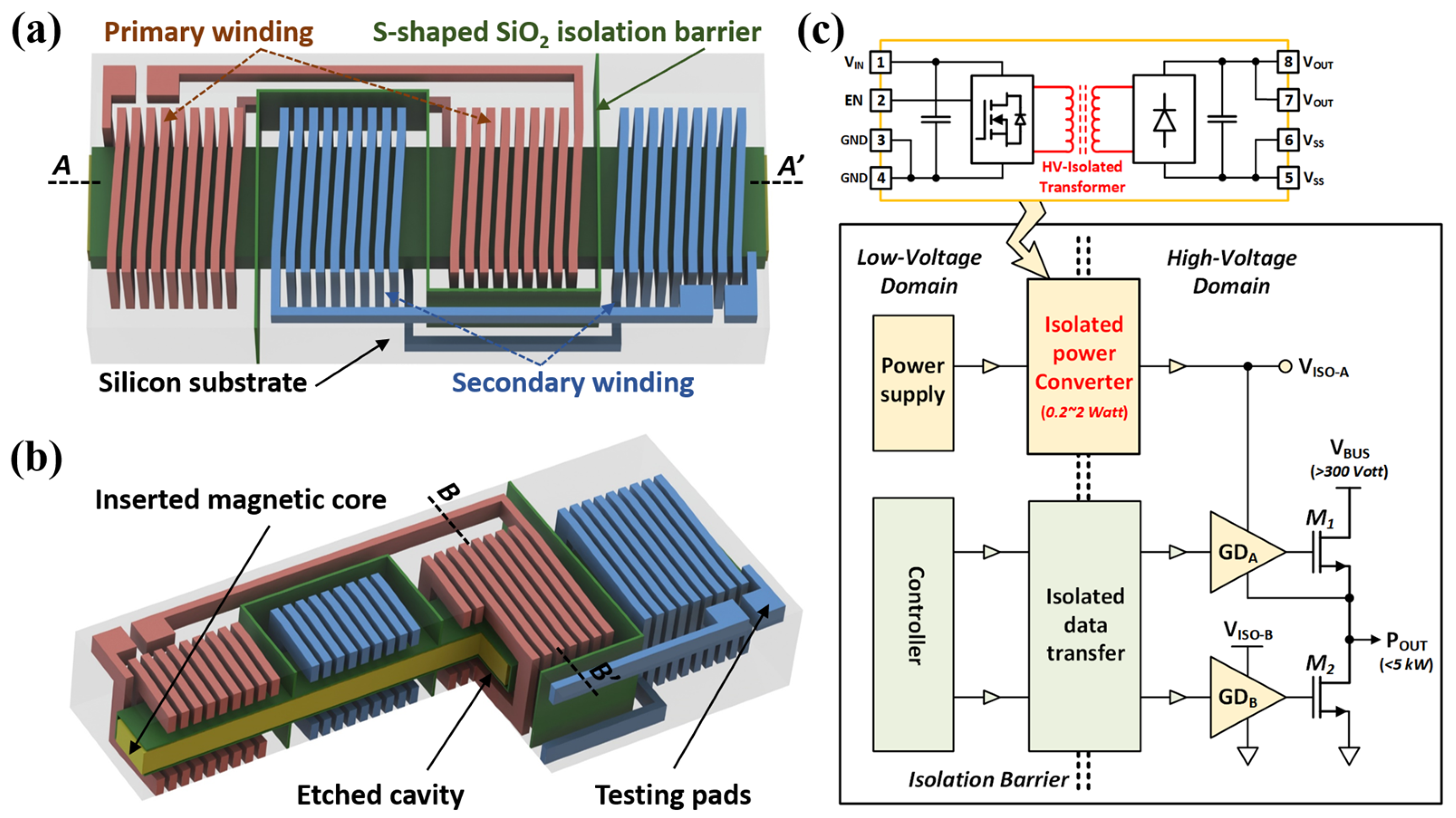
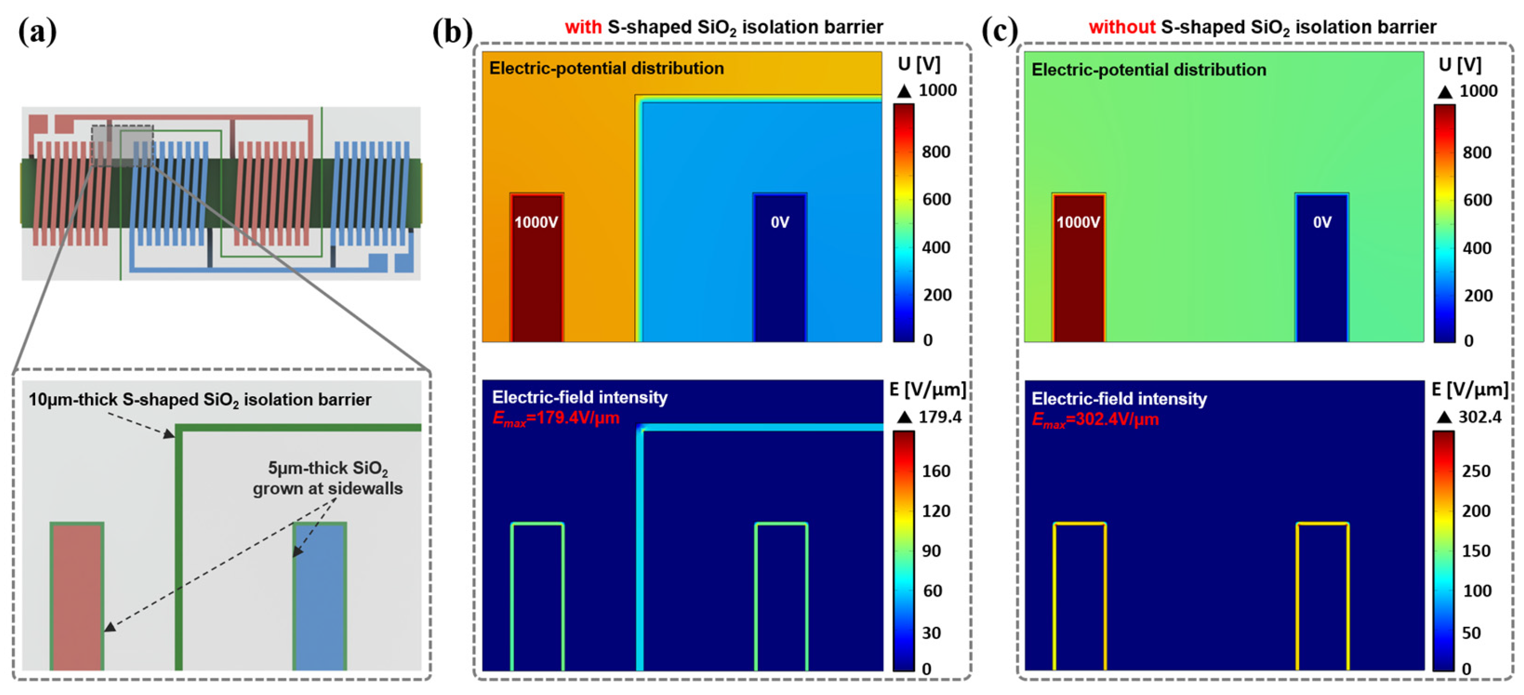
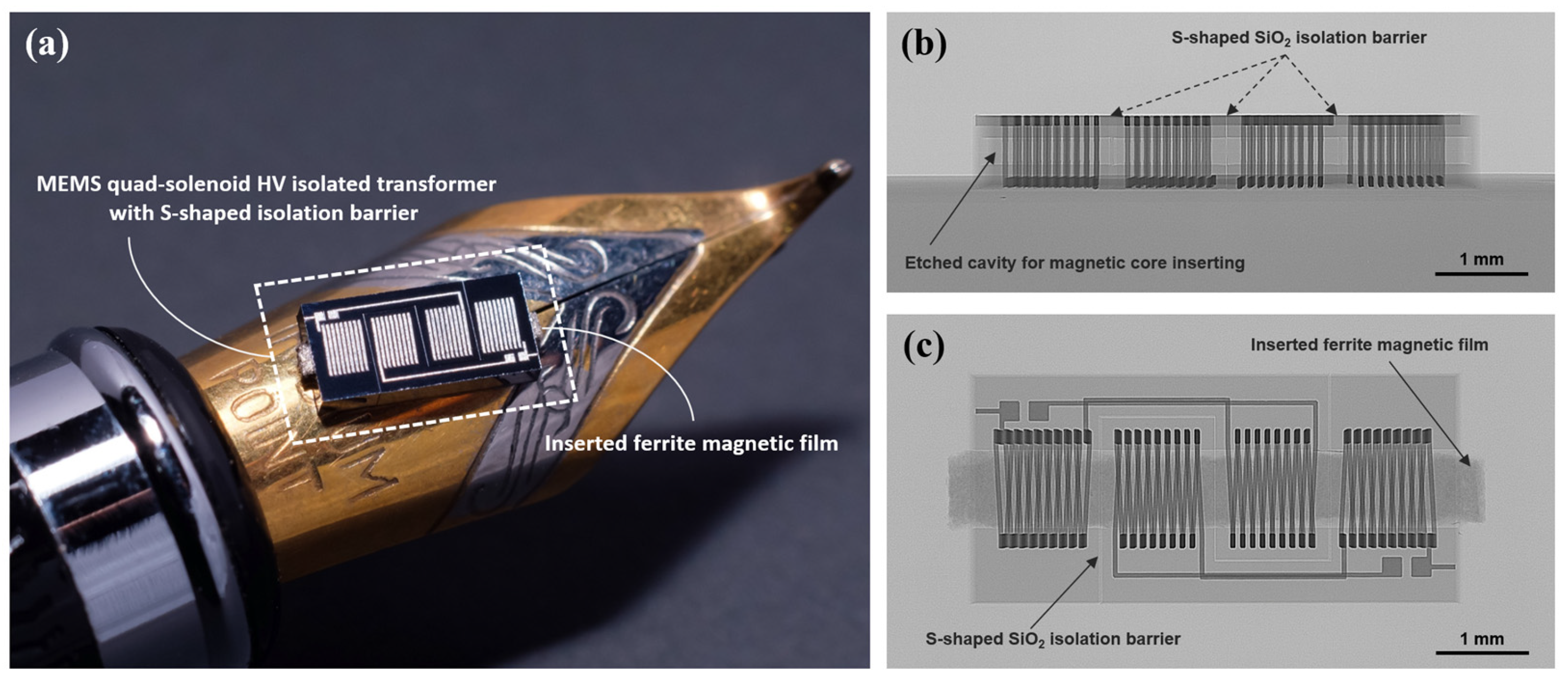
2.1. Structural Design of the High-Voltage-Isolated Transformer Device
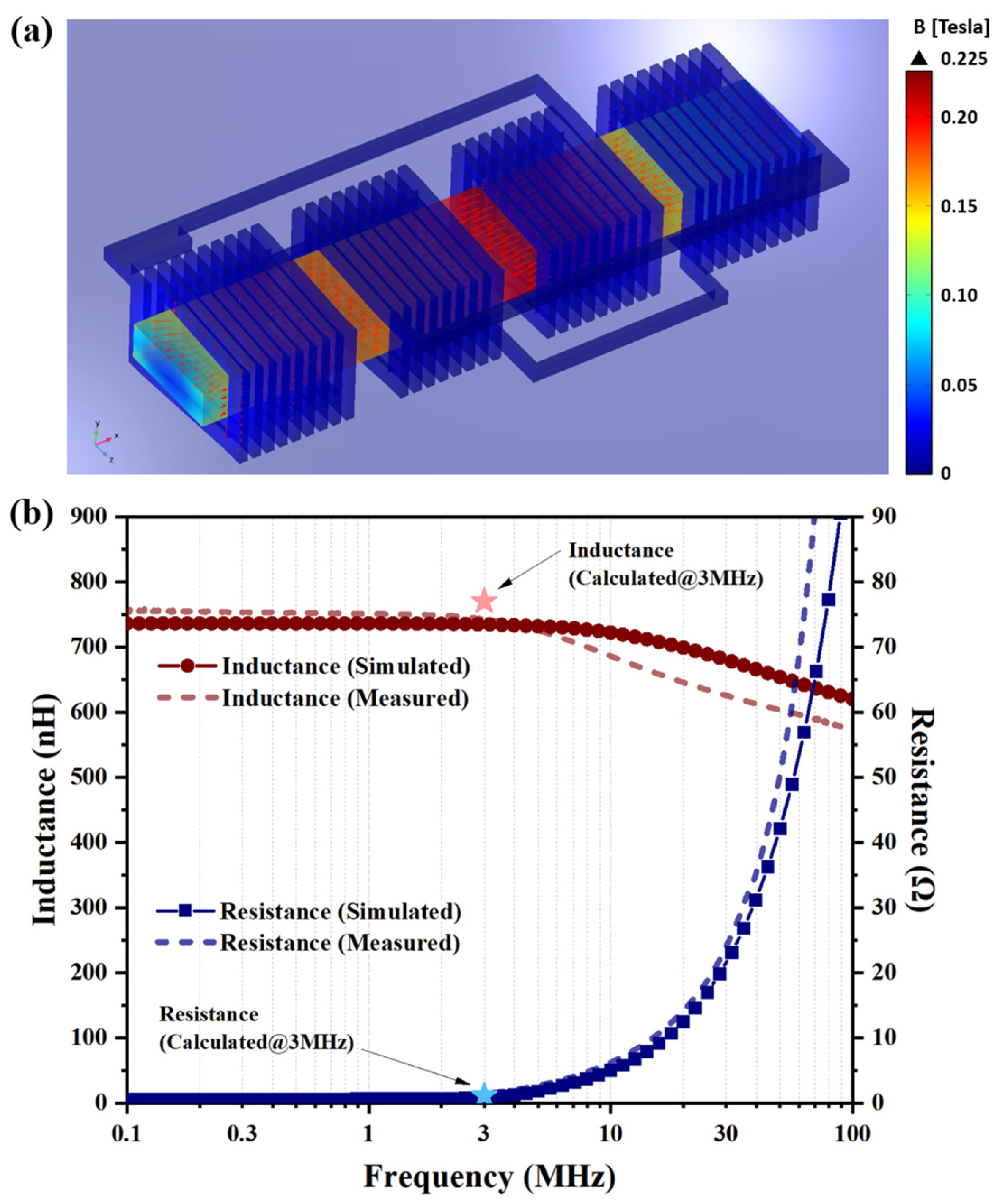
2.2. Device Modeling
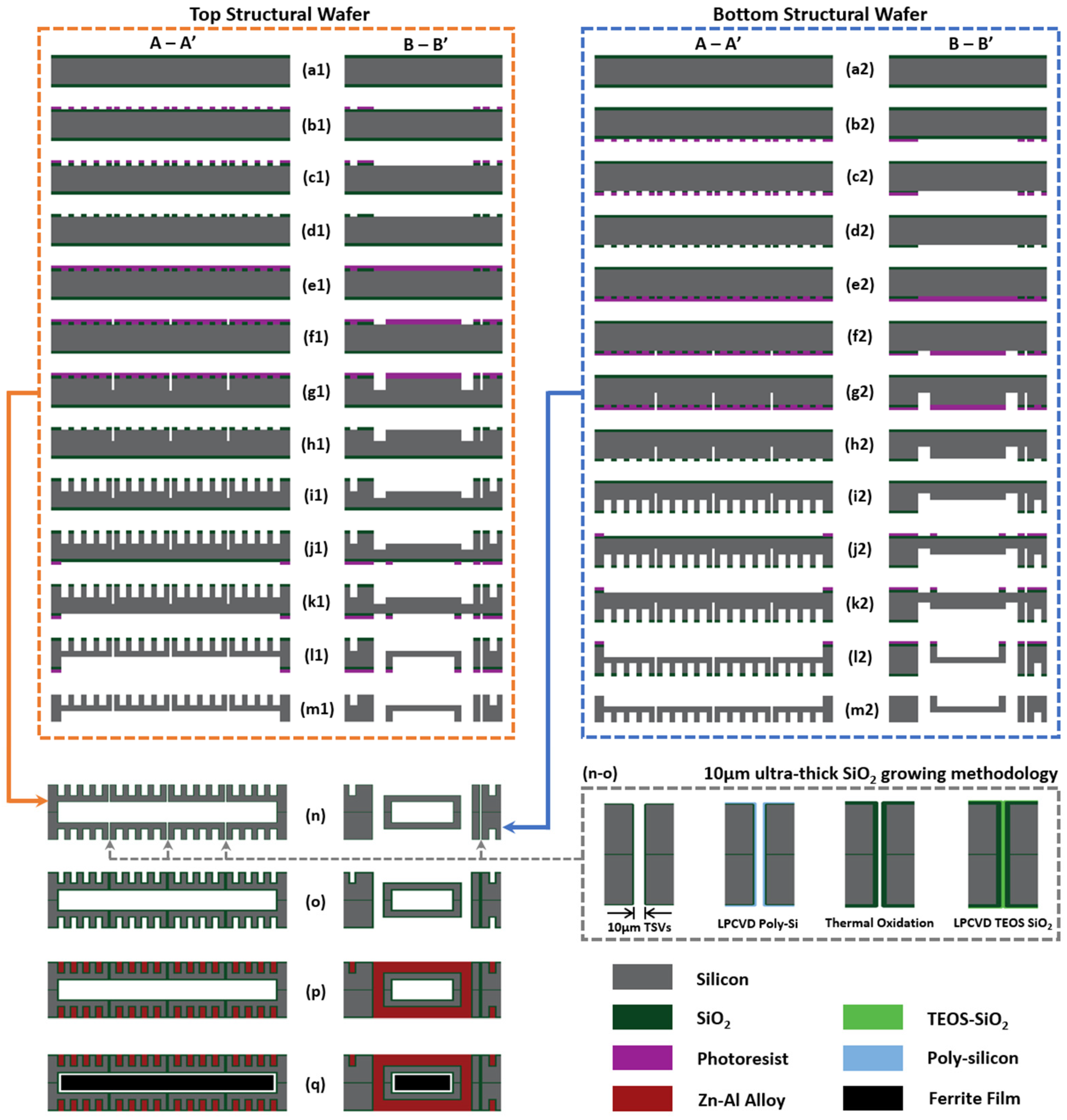
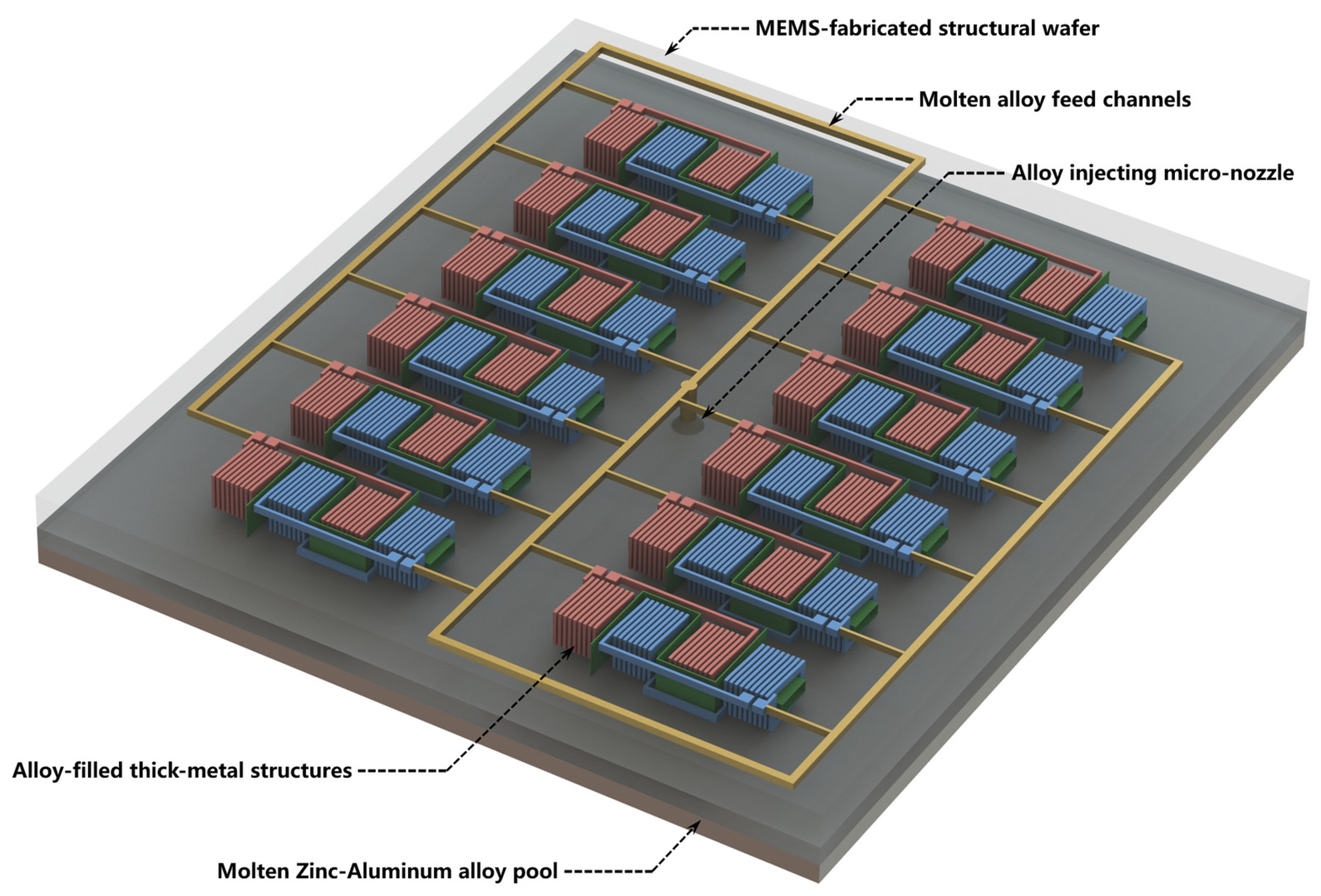
3. Fabrication
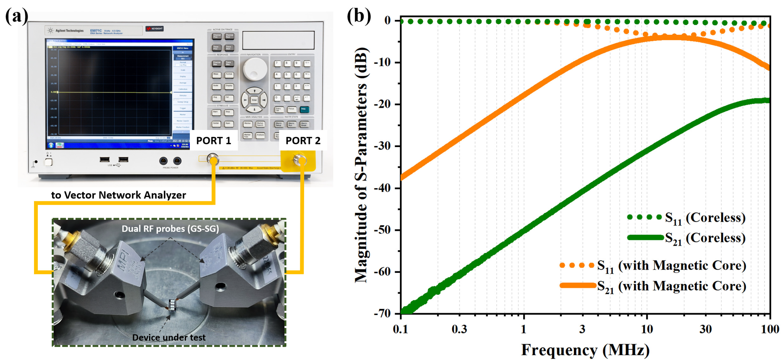
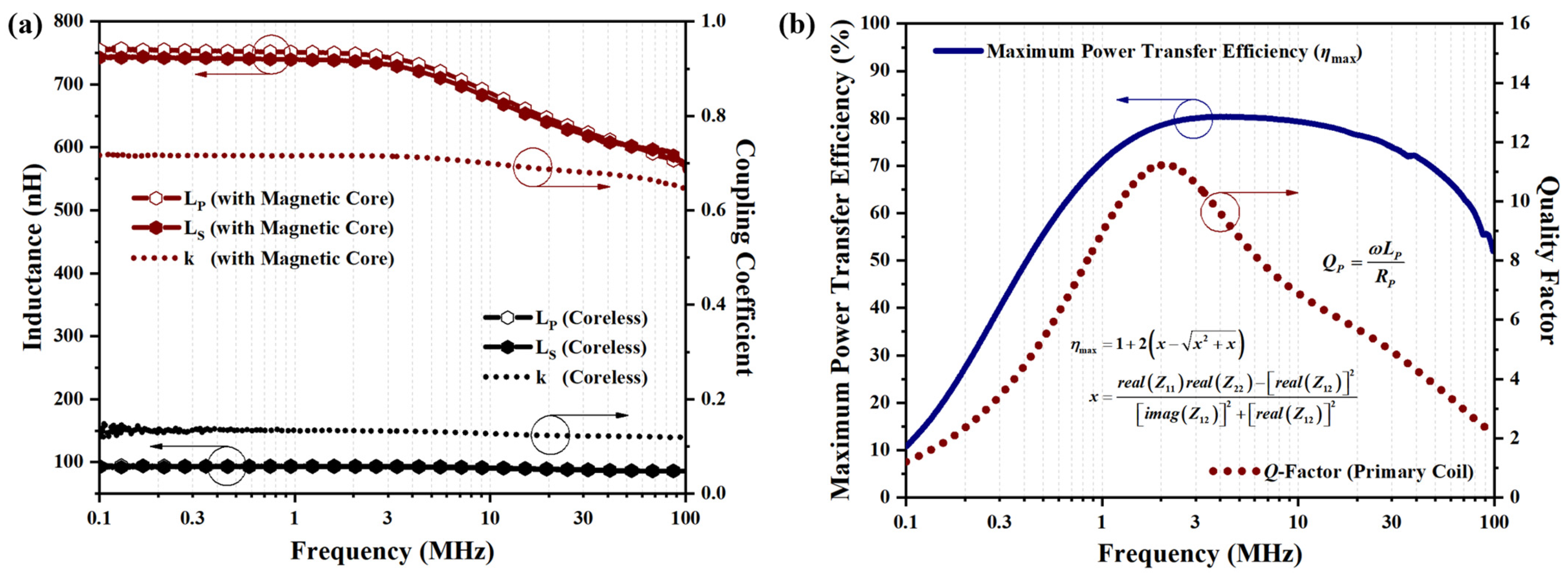
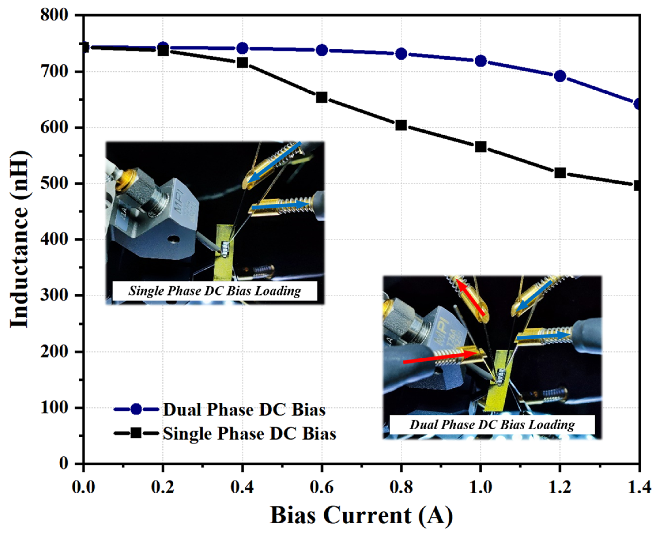
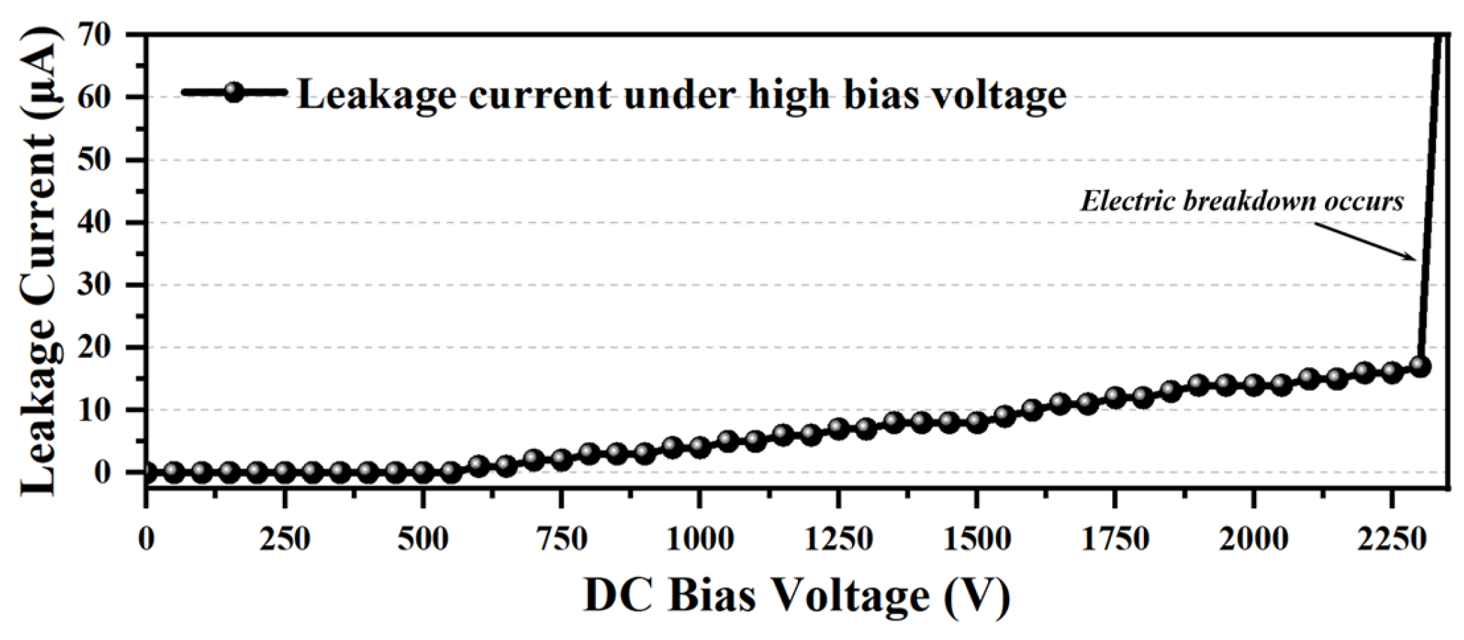
4. Testing Results
5. Conclusions
Author Contributions
Funding
Data Availability Statement
Acknowledgments
Conflicts of Interest
References
- Husain, I.; Ozpineci, B.; Islam, M.S.; Gurpinar, E.; Su, G.J.; Yu, W.; Chowdhury, S.; Xue, L.; Rahman, D.; Sahu, R. Electric Drive Technology Trends, Challenges, and Opportunities for Future Electric Vehicles. Proc. IEEE 2021, 109, 1039–1059. [Google Scholar] [CrossRef]
- Sato, E.K.; Kinoshita, M.; Sanada, K. Double DC-DC converter for uninterruptible power supply applications. In Proceedings of the 2010 International Power Electronics Conference—ECCE ASIA, Sapporo, Japan, 21–24 June 2010; pp. 635–642. [Google Scholar]
- Gayithri, C.; Dhanalakshmi, R. Analysis of power quality on a renewable energy micro grid conversion system with current and power controller. In Proceedings of the 2016 International Conference on Advanced Communication Control and Computing Technologies (ICACCCT), Ramanathapuram, India, 25–27 May 2016; pp. 449–453. [Google Scholar]
- Saeed, M.H.; Fangzong, W.; Kalwar, B.A.; Iqbal, S. A Review on Microgrids’ Challenges & Perspectives. IEEE Access 2021, 9, 166502–166517. [Google Scholar] [CrossRef]
- Millán, J.; Godignon, P.; Perpiñà, X.; Pérez-Tomás, A.; Rebollo, J. A Survey of Wide Bandgap Power Semiconductor Devices. IEEE Trans. Power Electron. 2014, 29, 2155–2163. [Google Scholar] [CrossRef]
- Gurpinar, E.; Chowdhury, S.; Ozpineci, B.; Fan, W. Graphite-Embedded High-Performance Insulated Metal Substrate for Wide-Bandgap Power Modules. IEEE Trans. Power Electron. 2021, 36, 114–128. [Google Scholar] [CrossRef]
- Wang, N.; Miftakhutdinov, R.; Kulkarni, S.; O’Mathuna, C. High Efficiency on Si-Integrated Microtransformers for Isolated Power Conversion Applications. IEEE Trans. Power Electron. 2015, 30, 5746–5754. [Google Scholar] [CrossRef]
- Ragonese, E.; Parisi, A.; Spina, N.; Palmisano, G. Fully Integrated Galvanically Isolated DC-DC Converters Based on Inductive Coupling. In Proceedings of the Applications in Electronics Pervading Industry; Environment and Society: Cham, Switzerland, 2019; pp. 335–341. [Google Scholar]
- Ragonese, E.; Spina, N.; Castorina, A.; Lombardo, P.; Greco, N.; Parisi, A.; Palmisano, G. A Fully Integrated Galvanically Isolated DC-DC Converter With Data Communication. IEEE Trans. Circuits Syst. Regul. Pap. 2018, 65, 1432–1441. [Google Scholar] [CrossRef]
- Ma, S.; Zhao, T.; Chen, B. 4A isolated half-bridge gate driver with 4.5V to 18V output drive voltage. In Proceedings of the 2014 IEEE Applied Power Electronics Conference and Exposition—APEC, Fort Worth, TX, USA, 16–20 March 2014; pp. 1490–1493. [Google Scholar] [CrossRef]
- Ragonese, E.; Spina, N.; Parisi, A.; Palmisano, G. An Experimental Comparison of Galvanically Isolated DC-DC Converters: Isolation Technology and Integration Approach. Electronics 2021, 10, 1186. [Google Scholar] [CrossRef]
- Panov, Y.; Jovanovic, M.M. Small-signal analysis and control design of isolated power supplies with optocoupler feedback. IEEE Trans. Power Electron. 2005, 20, 823–832. [Google Scholar] [CrossRef]
- Garcia, J.; Saeed, S.; Gurpinar, E.; Castellazzi, A.; Garcia, P. Self-Powering High Frequency Modulated SiC Power MOSFET Isolated Gate Driver. IEEE Trans. Ind. Appl. 2019, 55, 3967–3977. [Google Scholar] [CrossRef]
- Wu, R.; Sin, J.K.O.; Hui, S.Y. A novel silicon-embedded coreless transformer for isolated DC-DC converter application. In Proceedings of the 2011 IEEE 23rd International Symposium on Power Semiconductor Devices and ICs, San Diego, CA, USA, 23–26 May 2011; pp. 352–355. [Google Scholar]
- Khan, F.; Zhu, Y.; Lu, J.; Pal, J.; Dao, D.V. Micromachined Coreless Single-Layer Transformer Without Crossovers. IEEE Magn. Lett. 2015, 6, 6500404. [Google Scholar] [CrossRef]
- Wu, R.; Liao, N.; Fang, X.; Sin, J.K.O. A silicon-embedded transformer for high-efficiency, high-isolation, and low-frequency on-chip power transfer. IEEE Trans. Electron Devices 2015, 62, 220–223. [Google Scholar] [CrossRef]
- Chen, B. Fully integrated isolated DC-DC converter using micro-transformers. In Proceedings of the 2008 Twenty-Third Annual IEEE Applied Power Electronics Conference and Exposition—APEC, Austin, TX, USA, 24–28 February 2008; pp. 335–338. [Google Scholar] [CrossRef]
- Feeney, C.; Yu, J.; Peng, S.; Ye, T.; Yang, S.; Wang, N. Thin Film Magnetic Core Microinductor With Stacked Windings. IEEE Trans. Electron Devices 2021, 68, 4237–4241. [Google Scholar] [CrossRef]
- Cheng, M.; Liu, L.; Liao, Z.; Yu, J.; Peng, S.; Zhang, Z.; Ye, T.; Wang, N. On Silicon-Integrated Micro-Transformers and Their Applications in Quasi-Resonant Flyback Converters. IEEE Trans. Magn. 2022, 58, 8401209. [Google Scholar] [CrossRef]
- Mundotiya, B.M.; Dinulovic, D.; Rissing, L.; Wurz, M.C. Fabrication and characterization of a Ni-Fe-W core microtransformer for high-Frequency power applications. Sen. Actuators A Phys. 2017, 267, 42–47. [Google Scholar] [CrossRef]
- Ahmed, M.Z.; Bhuyan, M.S.; Islam, A.K.M.T.; Majlis, B.Y. Design and Fabrication of a MEMS 3D Micro-transformer for Low Frequency Applications. Asian J. Sci. Res. 2015, 8, 237–244. [Google Scholar] [CrossRef]
- Xing, X.; Sun, N.X.; Chen, B. High-bandwidth low-insertion loss solenoid transformers using FeCoB multilayers. IEEE Trans. Power Electron. 2013, 28, 4395–4401. [Google Scholar] [CrossRef]
- Gu, J.; Liu, B.; Chen, G.; Li, X. Study of a through-silicon/substrate via filling method based on the combinative effect of capillary action and liquid bridge rupture. J. Micromech. Microeng. 2016, 26, 075009. [Google Scholar] [CrossRef]
- Gu, J.; Liu, B.; Yang, H.; Li, X. A metal micro-casting method for through-silicon Via (TSV) fabrication. In Proceedings of the 2017 IEEE Electron Devices Technology and Manufacturing Conference (EDTM), Toyama, Japan, 28 February–2 March 2017; pp. 211–212. [Google Scholar]
- Lee, D.W.; Wang, S.X. Effects of geometries on permeability spectra of CoTaZr magnetic cores for high frequency applications. J. Appl. Phys. 2008, 103, 07E907. [Google Scholar] [CrossRef]
- Jun-Bo, Y.; Bon-Kee, K.; Chul-Hi, H.; Euisik, Y.; Kwyro, L.; Choong-Ki, K. High-performance electroplated solenoid-type integrated inductor (SI2) for RF applications using simple 3D surface micromachining technology. In Proceedings of the International Electron Devices Meeting 1998. Technical Digest (Cat. No.98CH36217), San Francisco, CA, USA, 6–9 December 1998; pp. 544–547. [Google Scholar]
- Chen, D.X.; Brug, J.A.; Goldfarb, R.B. Demagnetizing factors for cylinders. IEEE Trans. Magn. 1991, 27, 3601–3619. [Google Scholar] [CrossRef]
- Chen, D.X.; Pardo, E.; Sanchez, A. Demagnetizing factors of rectangular prisms and ellipsoids. IEEE Trans. Magn. 2002, 38, 1742–1752. [Google Scholar] [CrossRef]
- Harrington, R.F. Time-Harmonic Electromagnetic Fields; McGraw-Hill: New York, NY, USA, 1961. [Google Scholar]
- Lee, D.W.; Hwang, K.P.; Wang, S.X. Fabrication and Analysis of High-Performance Integrated Solenoid Inductor With Magnetic Core. IEEE Trans. Magn. 2008, 44, 4089–4095. [Google Scholar] [CrossRef]
- Reatti, A.; Kazimierczuk, M.K. Comparison of various methods for calculating the AC resistance of inductors. IEEE Trans. Magn. 2002, 38, 1512–1518. [Google Scholar] [CrossRef]
- Guevara-Morales, A.; Taylor, A.C. Mechanical and dielectric properties of epoxy-clay nanocomposites. J. Mater. Sci. 2014, 49, 1574–1584. [Google Scholar] [CrossRef]
- Muramoto, Y.; Shimizu, N.; Fukuma, M.; Nagao, M. Effect of space charge on conduction current and breakdown of polyimide films. In Proceedings of the 8th IEEE International Conference on Solid Dielectrics, Toulouse, France, 5–9 July 2004; pp. 41–44. [Google Scholar]
- Modafe, A.; Ghalichechian, N.; Kleber, B.; Ghodssi, R. Electrical characterization of BCB for electrostatic microelectromechanical devices. In Proceedings of the Symposium on Micro- and Nanosystems held at the 2003 MRS Fall Meeting, Boston, MA, USA, 1–3 December 2004; pp. 305–310. [Google Scholar]
- Rojas, S.; Modelli, A.; Wu, W.S.; Borghesi, A.; Pivac, B. Properties of Silicon Dioxide Films Prepared by Low-Pressure Chemical Vapor-Deposition from Tetraethylorthosilicate. J. Vac. Sci. Technol. B 1990, 8, 1177–1184. [Google Scholar] [CrossRef]
- Ghodssi, R.; Lin, P. MEMS Materials and Processes Handbook; Springer Science & Business Media: Berlin, Germany, 2011; Volume 1. [Google Scholar]
- Frickey, D.A. Conversions Between S, Z, Y, h, ABCD, and T Parameters which are Valid for Complex Source and Load Impedances. IEEE Trans. Microw. Theory Tech. 1994, 42, 205–211. [Google Scholar] [CrossRef]
- Wu, R.; Liao, N.; Fang, X.; Cai, J.; Wang, Q.; Sin, J.K.O. A 3D Assembled Silicon-Embedded Transformer for 10-MHz, Ultra-High-Isolation, Compact Chip-to-Chip Power Transfer. IEEE Electron Device Lett. 2017, 38, 356–358. [Google Scholar] [CrossRef]
- Wang, N.; Kulkarni, S.; Jamieson, B.; Rohan, J.; Casey, D.; Roy, S.; Mathuna, C.O. High efficiency Si integrated micro-transformers using stacked copper windings for power conversion applications. In Proceedings of the 2012 Twenty-Seventh Annual IEEE Applied Power Electronics Conference and Exposition (APEC), Orlando, FL, USA, 5–9 February 2012; pp. 411–416. [Google Scholar]
- Li, H.; Zhu, K.; Lei, K.; Xu, T.; Wu, H. Integrated MEMS Toroidal Transformer With Ni-Zn Ferrite Core for Power Supply on Chip. IEEE Trans. Power Electron. 2022, 37, 10075–10080. [Google Scholar] [CrossRef]
- Wu, R.; Liao, N.; Fang, X.; Sin, J.K.O. A Novel Double-Side Silicon-Embedded Transformer for 10-MHz, 1-kV-Isolation, Compact Power Transfer Applications. IEEE Trans. Electron Devices 2016, 63, 4542–4545. [Google Scholar] [CrossRef]
- Ng, K.T.; Rejaei, B.; Burghartz, J.N. Substrate effects in monolithic RF transformers on silicon. IEEE Trans. Microw. Theory Tech. 2002, 50, 377–383. [Google Scholar] [CrossRef]
- He, Y.; Wu, R.; Zhong, Z.; Zhang, H.; Bai, F. On-Chip Coupled Solenoid Inductors for Integrated Power Conversion. IEEE Trans. Electron Devices 2021, 68, 6292–6295. [Google Scholar] [CrossRef]


| Parameters | Primary Winding | Secondary Winding |
|---|---|---|
| Number of turns (N1 + N2) | 18 (9 + 9) | 18 (9 + 9) |
| Metal width | 60 μm | 60 μm |
| Metal depth | 100 μm | 100 μm |
| Gap between adjacent turns | 40 μm | 40 μm |
| Coil inner height | 520 μm | 520 μm |
| Coil inner width | 900 μm | 900 μm |
| Parameters | Inserted thin-film ferrite magnetic core | |
| Max relative permeability (at 3 MHz) | 185 (real part, μ’); 13 (imaginary part, μ’’) | |
| Length of the magnetic core | 5100 μm | |
| Width of the magnetic core | 700 μm | |
| Thickness of the magnetic core | 200 μm | |
| Epoxy | Polyimide | BCB | LPCVD TEOS SiO2 | Thermal SiO2 | |
|---|---|---|---|---|---|
| Dielectric strength | 11.7 V/μm [32] | 300 V/μm [33] | 320 V/μm [34] | 500 V/μm [35] | 500 V/μm [36] |
| Parameter | [38] | [39] | [40] | [41] | [20] | This Work |
|---|---|---|---|---|---|---|
| Magnetic core | Non | Yes | Yes | Non | Yes | Yes |
| Insulating materials | BCB | BCB | SiO2 | SiO2 | PI | SiO2 |
| Frequency (MHz) | 10 | 20 | 14 | 10 | 70 | 3 |
| Inductance (nH) | 159 | 80 | 114.9 | 113 | 47 | 743.2 |
| Inductance density (nH/mm2) | 79.5 | 22.85 | 8.64 | 56.5 | 10.44 | 123.9 |
| Coupling coefficient | 0.64 | N/A | 0.70 | 0.65 | 0.65 | 0.72 |
| DC resistance (Ω) | 0.4 | 0.34 | 0.15 | 0.31 | 0.5 | 0.39 |
| L/R (nH/Ω) | 398 | 235 | 766 | 360 | 94 | 1906 |
| Isolation voltage (V) | 4500 | N/A | N/A | 1050 | 500 | 2300 |
| Max power transfer efficiency | 70% | 37% | N/A | 70% | 68% | 80% |
Disclaimer/Publisher’s Note: The statements, opinions and data contained in all publications are solely those of the individual author(s) and contributor(s) and not of MDPI and/or the editor(s). MDPI and/or the editor(s) disclaim responsibility for any injury to people or property resulting from any ideas, methods, instructions or products referred to in the content. |
© 2024 by the authors. Licensee MDPI, Basel, Switzerland. This article is an open access article distributed under the terms and conditions of the Creative Commons Attribution (CC BY) license (https://creativecommons.org/licenses/by/4.0/).
Share and Cite
Chen, C.; Pan, P.; Gu, J.; Li, X. A High-Voltage-Isolated MEMS Quad–Solenoid Transformer with Specific Insulation Barriers for Miniaturized Galvanically Isolated Power Applications. Micromachines 2024, 15, 228. https://doi.org/10.3390/mi15020228
Chen C, Pan P, Gu J, Li X. A High-Voltage-Isolated MEMS Quad–Solenoid Transformer with Specific Insulation Barriers for Miniaturized Galvanically Isolated Power Applications. Micromachines. 2024; 15(2):228. https://doi.org/10.3390/mi15020228
Chicago/Turabian StyleChen, Changnan, Pichao Pan, Jiebin Gu, and Xinxin Li. 2024. "A High-Voltage-Isolated MEMS Quad–Solenoid Transformer with Specific Insulation Barriers for Miniaturized Galvanically Isolated Power Applications" Micromachines 15, no. 2: 228. https://doi.org/10.3390/mi15020228