1. Introduction
A radio frequency energy harvester (RFEH)–based system on chip (SoC) is an integrated circuit that is capable of operating with much less dependency on battery energy [
1]. It is made up of many different sub-circuit blocks, such as analog and mixed signal blocks, and each one requires a different voltage domain from the power source, which has high power quality requirements. Hence, RFEH can extend the life of battery-powered SoCs.
A wireless sensor node (WSN), on the other hand, which is made up of four major components—a sensing unit, a power unit, a processing unit, and a transmitter—requires a better power solution to extend the battery life of the sensor, which continuously monitors, captures, and transmits data to the processing unit for processing [
2,
3]. Each wireless sensor node component operates in a different voltage domain.
Besides this, a series of prominent microcontrollers widely used in the industry still require a dynamic voltage scaling power solution. The microcontrollers have a supply voltage range that varies based on the system frequency. For example, flash memory programming is not necessary for microcontrollers, such as MSP430G2001, when the system frequency is 1 MHz. During this phase, the supply voltage range is from 1.8 V to 3.6 V. Meanwhile, the supply voltage range is from 2.2 V to 3.6 V if flash memory programming is needed [
2,
4]. The static or single-power solution is not helpful in such conditions. A notable power solution is required for the system to increase its power efficiency.
A single-inductor multiple-output (SIMO) device that switches out multiple independent DC/DC converters could be the solution for multi-voltage domains [
5,
6,
7]. The SIMO DC/DC converter can regulate multiple outputs while maintaining high power efficiency thanks to a single internal inductor component. The SIMO approach has an advantage over traditional DC/DC regulators in that it consumes less power and occupies less chip area than traditional methods, which necessitate the use of multiple independent regulators to supply multiple domains. Although this strategy helps to increase power efficiency, large off-chip inductors prevent its use in SoC architecture because they take up a lot of space. Aside from that, output ripples, switching noise, and cross regulation from the switching regulator, as well as the failure to provide a clean supply to the device, are significant flaws in this solution.
In the last decade, the power management integrated circuit (PMIC), consisting of a switching regulator and several low-dropout regulators, has sparked much interest as a multi-voltage domain solution. Even though switching regulators do not provide clean power, they are more efficient than LDOs in terms of the massive voltage drop from input to output. Because the switching regulator’s output must be ripple-free, the LDO is a good solution for providing clean power because of its high power supply rejection capability. Both regulators were built as a single integrated circuit to improve power efficiency and reduce ripple in the regulated voltage. LDOs are placed in the back end and switching regulators are placed in the front end. However, when used for an embedded or SoC solution, the complexity of fabricating inductors for PMIC is a significant disadvantage [
8]. Furthermore, PMIC is better suited for high-power systems than low-power solutions.
Because LDO can provide a clean supply with a strong supply rejection ability, it is a popular alternative to PMIC for supplying different voltages for SoC system applications [
9]. However, a large external capacitor was placed at the output LDO to reduce overshoot and undershoot while maintaining stability. This is difficult for SoC applications due to space constraints. The use of capacitorless, OCL-LDO to overcome area constraints is ideal for portable electronic devices and SoC power delivery applications. However, to support multiple voltage domain operations in SoC, typically multiple LDOs are needed to accommodate in the SoC, which consumes more area on the SoC chip. Furthermore, power efficiency in numerous independent LDO have deteriorated because all LDO consume power continuously, even if some voltage domains only operate infrequently and do not require constant supply [
10].
In addition to multiple independent LDO, researchers are interested in designing LDO with programmable output voltage [
11,
12,
13]. The output voltage was varied by changing the ratio of the feedback resistor via the transistor switch. The control signal activated and deactivated the transistor switch. The programmable output voltage topologies in the cited paper [
11,
12,
13] used control logic, consisting of many CMOS switches in the feedback network, to vary the output voltage. Various topologies such as multi-voltage control, adaptive reference control, dynamic voltage, and frequency scaling were used to control the gate voltage of the CMOS switches to achieve the desired output voltage of LDO. These circuits consume a large area on the chip.
J. H. Wang et al. proposed a programmable 32-step output voltage that modifies the digital pulse width modulation (DPWM) clock and supplies it with a clean supply voltage [
14]. The output voltage was modified using digital LDO topology in this technique. The phase frequency detector detected the clock differences between the reference clock and DPWM output clock. The output clock of DPWM was fed into the phase-frequency detector, PFD. When the output clock of DPWM differs from the reference clock in frequency or phase, the PFD captures it and generates a voltage signal to indicate the variation in phase or frequency. The main objective of the TDC employed in this design is to convert the output of the PFD signal into a 5-bit digital signal, which is then used to correct the output clock of the DPWM by adjusting the output voltage of the proposed LDO regulator, as explained in reference [
14].
A higher resolution of step size is also necessary for DLDO to ensure that the output voltage is regulated with high accuracy. Moderate step size or step resolution leads to drawbacks in output voltage accuracy [
14]. However, high power consumption and a large chip area are the trade-offs for the high-resolution step circuit. Hence, a technique for programmable reference voltage with a wider input common mode error amplifier has been introduced in addition to programmable output voltage LDO [
15,
16].
To address the issues above, the MVD-LDO has been proposed in this work. The proposed MVD-LDO has an on-chip capacitor and can handle up to 400 mA load current, making it suitable for embedded and SoC applications.
Section 2 and
Section 3 describe the application and circuit architecture of the proposed multi-voltage domain low dropout regulator with demultiplexer, followed by
Section 4, which elaborates on circuit implementation of multi-voltage domain LDO.
Section 5 displays the measurement results of the proposed design, and
Section 6 presents the conclusion.
3. Circuit Architecture of MVD-LDO
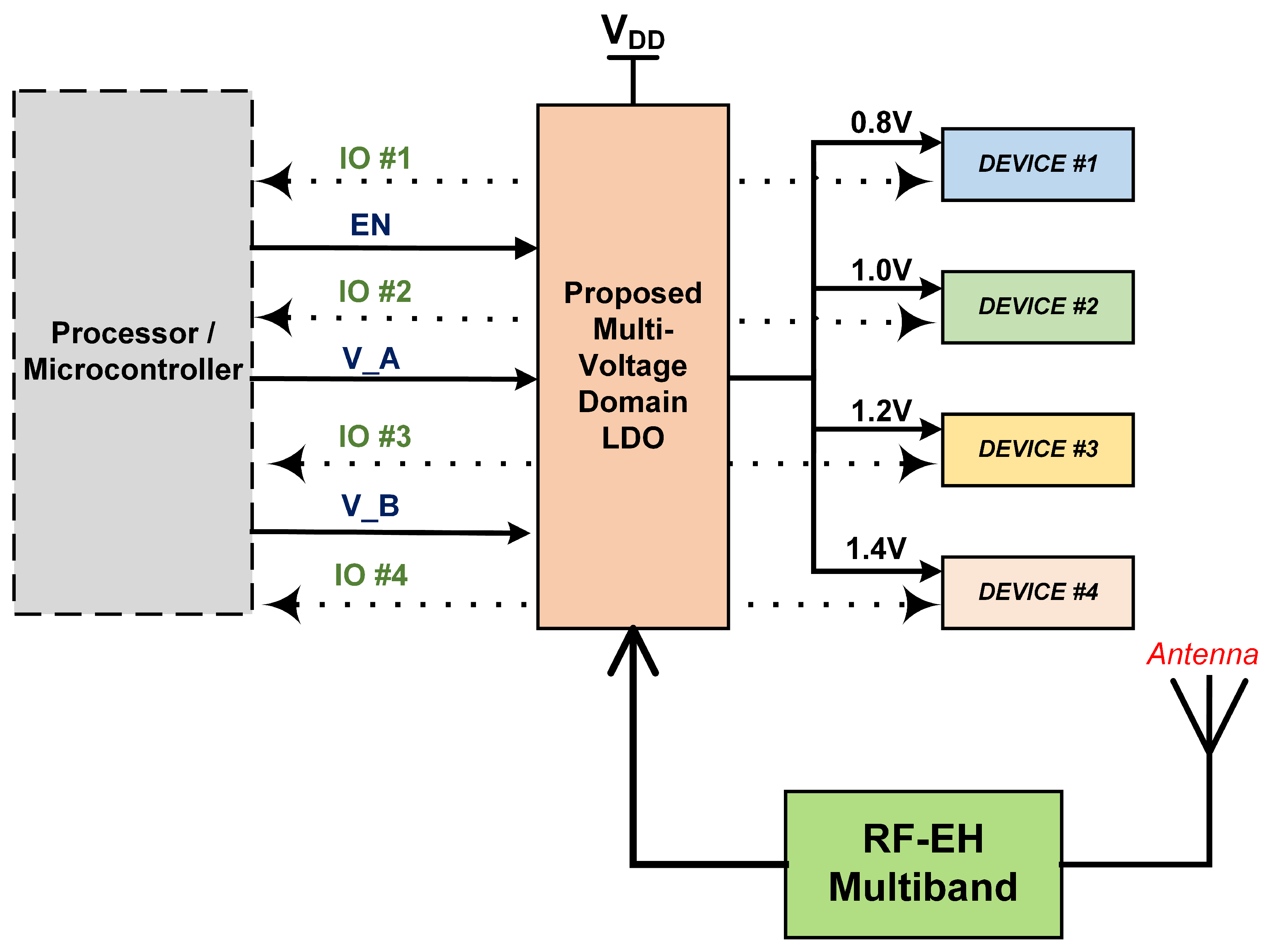
Figure 2 illustrates the schematic of the MVD-LDO which is capable of producing up to four regulated output voltages (Vout 1, 2, 3, 4) with a DEMUX controller.
This MVD- LDO regulator comprises a set of feedback resistors, a pass element, a low-power error amplifier, bandgap reference voltage (BGR), demultiplexer, and on-chip load capacitor. A resistive divider of the output voltage generates the feedback voltage, VFB, which varies proportionally with the output voltage. A reference voltage, VREF, is supplied through the bandgap reference (BGR) circuit. When the feedback voltage, VFB, deviates from the reference voltage, VREF, the error amplifier is used to correct the error at the output voltage by adjusting the gate voltage of the pass device. The error amplifier corrects errors by varying the pass transistor’s gate voltage and assuring the regulated voltage is within design parameters.
The feedback circuit in the proposed MVD-LDO consists of R1, R2A, R2B, R2C, and R2D to provide four output voltages. In addition, for switching purposes, an NMOS transistor has been added to each pathway of the feedback resistor. In response to user input, the demultiplexer activated the gate voltage of an NMOS transistor. Only one output voltage can be regulated at any given time. The constituent units are discussed in the following sections.
4. Circuit Implementation of MVD-LDO
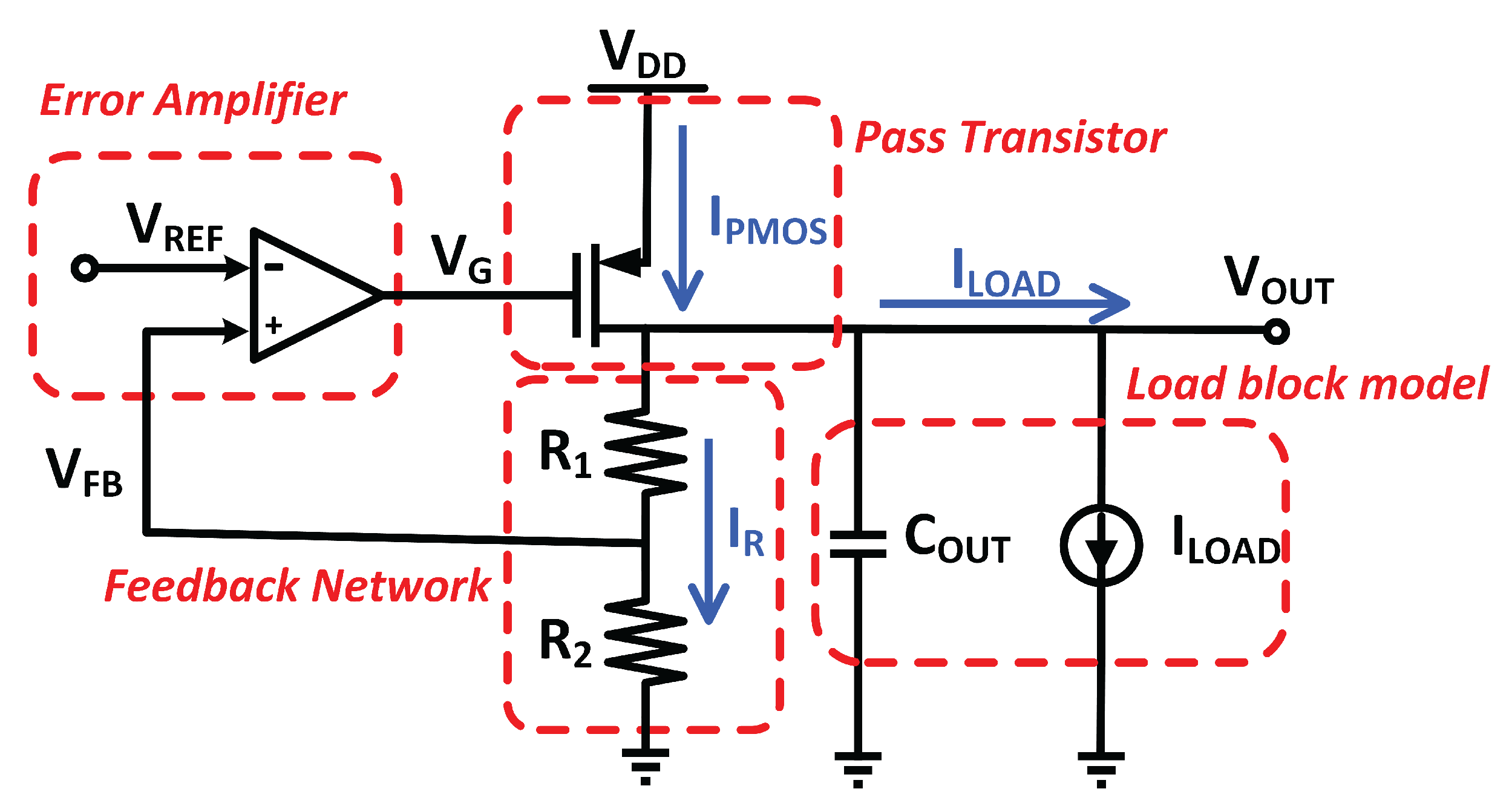
Figure 3 depicts a single voltage domain LDO with the output voltage controlled by feedback resistors or the reference voltage of the op-amp [
17].
The LDO’s V
out is given as:
where V
FB, is the feedback voltage of the single voltage domain LDO. The error amplifier regulates the gate voltage of the pass transistor by comparing V
FB to the reference voltage, V
REF. If an error amplifier’s input is unequal, the pass transistor’s gate voltage is varied to control the required output voltage. This activity loops indefinitely to ensure that the output voltage is accurately regulated.
Off-chip placement of the feedback resistor is common, and the combination of feedback resistor values is positioned according to the desired regulated output voltage. Unfortunately, using an off-chip approach raises the design cost and is unsuitable for embedded design. Aside from that, an incorrect resistor value influences the regulator’s current efficiency, stability, and other critical parameters, resulting in a system with poor power efficiency.
Altering the reference voltage, V
REF, while preserving the feedback resistor’s ratio is an additional way for altering the output voltage [
17]. Since the reference voltage usually supplied from the bandgap reference, which is conspicuous across the process, voltage, and temperature, and tweaking the reference voltage is not a good solution to achieve acceptable output voltage. Hence, in MVD-LDO, adjusting the feedback resistor ratio has been adopted to govern the multi-voltage domain.
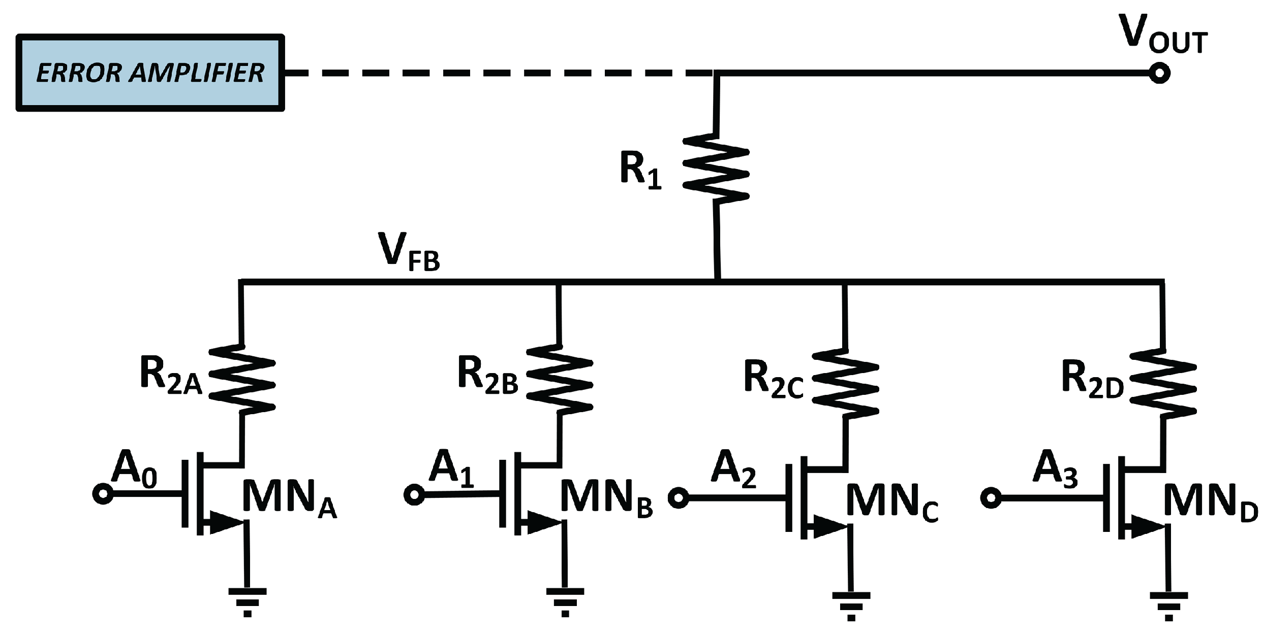
Figure 4 displays the design of the MVD-feedback LDO’s resistor.
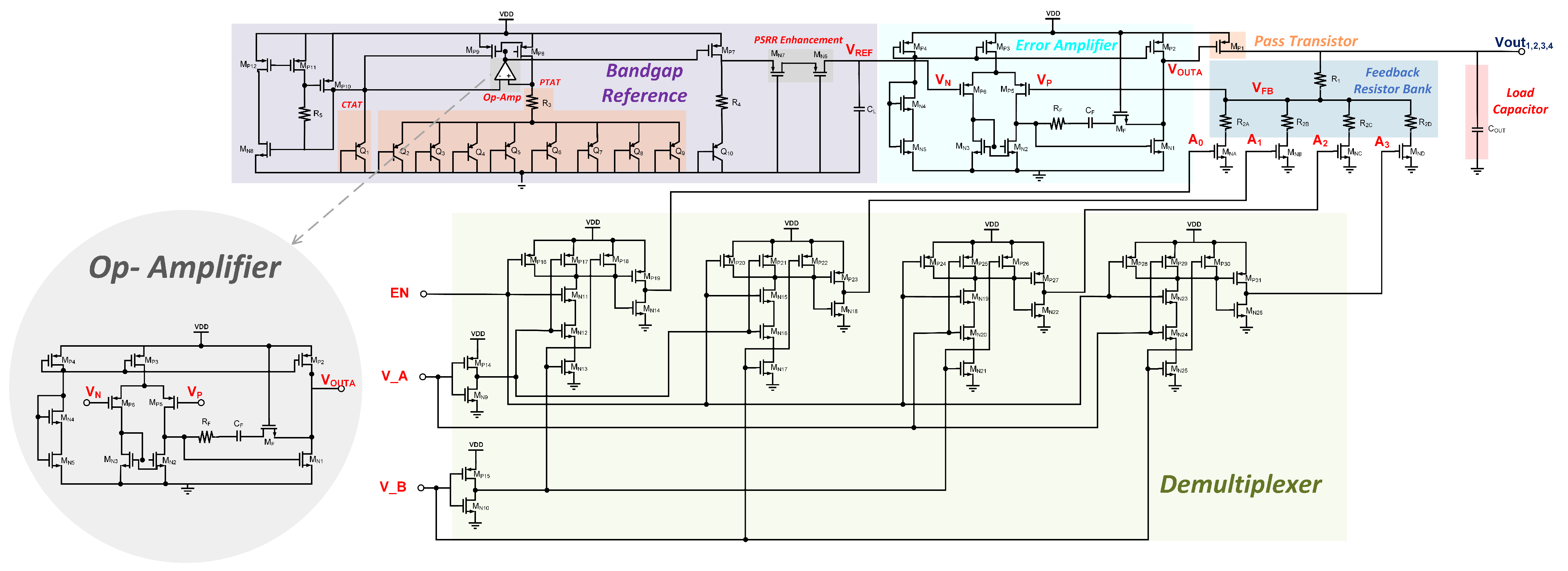
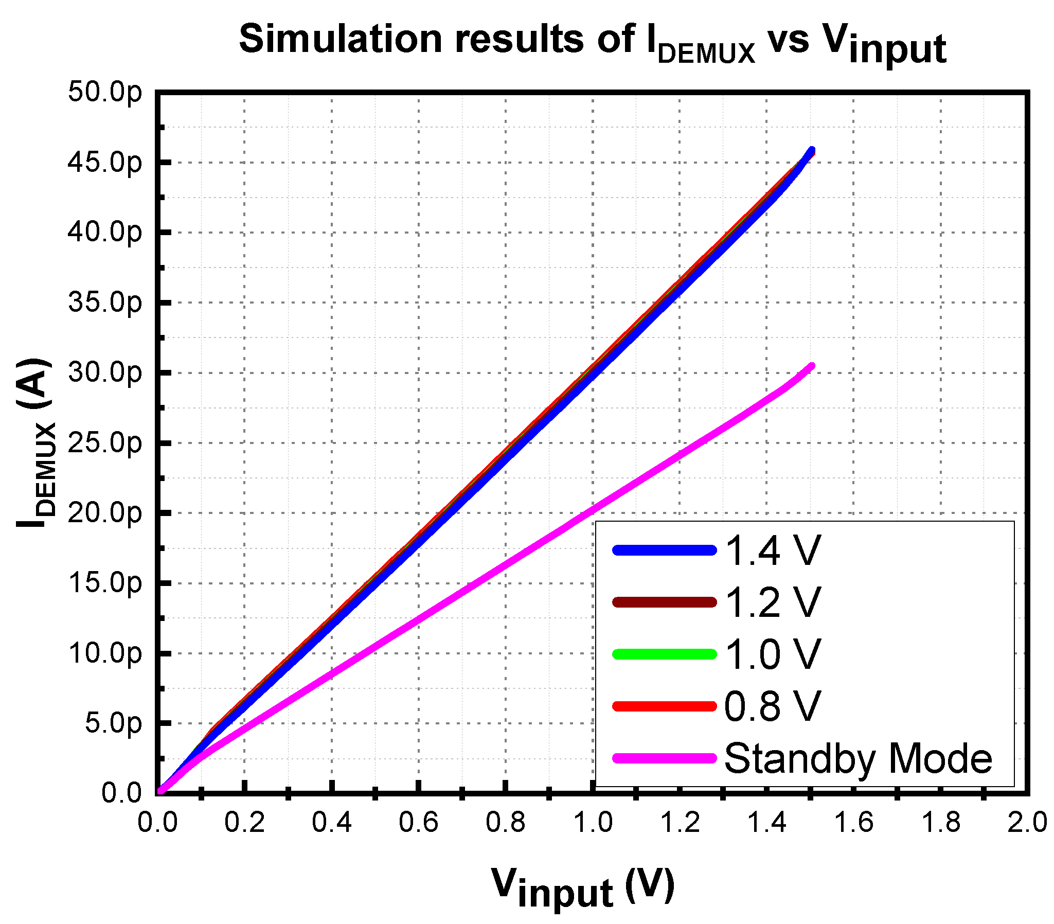
In our work, the bottom resistor of the feedback network circuit has been developed using a resistor bank, which increases the precision of the output voltage and offers multiple Vout. Since this design intends to handle four Vout, a total of four resistors, R2A, R2B, R2C, and R2D, have been added to the bottom of the feedback resistor. NMOS transistors MNA, MNB, MNC, and MND serve as switches. At a given moment, only one path is activated. In accordance with the ratio of the feedback resistor in the active circuit, the output voltage is regulated. An on-chip low power consumption demultiplexer design has been implemented to manage the switches and adjust the output voltage correspondingly. The power consumption of the DEMUX is only 68.85 pW. This is considered in the worst-case scenario, when all three inputs of the DEMUX have been turned on.
The digital 2:4 demultiplexer has been utilized on the proposed MVD-LDO. This demultiplexer uses three input signals, which are one enable pin and two logic input pins, to generate four output signals that regulate the feedback network’s switched-on state. A0, A1, A2, and A3 are the demultiplexer’s output signals, whereas V_A, V_B, and EN are the input signals
Similar to VDD, the input voltage of the demultiplexer is 1.5 V. The enable pin, EN, is employed to activate the LDO regulator. If the EN signal logic is LOW, the DEMUX is powered off as all four switches are turned off. Therefore, VFB is the same as VDD. As a result, the gate voltage of the pass devices rises as the error amplifier’s output voltage increases, resulting in the eventual shutdown of the LDO. The shutdown process puts the SoC into sleep mode, critical for conserving battery energy.
To achieve low power consumption, the W/L of the demultiplexer’s transistors are optimized with reference to (2):
As a result, the demultiplexer consumes only 30.5 pA and 45.9 pA of current in standby and operating modes, respectively. The EN is used to toggle between operating and standby mode. The simulation results of the current consumption of the demultiplexer during standby and operating modes are shown in
Figure 5. The simulation was performed on the Cadence Virtuoso platform with Silterra CMOS 180 nm process technology.
Most of the logic gate was shut down during standby mode since the EN signal is low. Therefore, it consumes minimal current. On the other hand, when all logic is enabled, the current consumption rises rapidly. In the proposed MVD-LDO, the EN, V_A, and V_B must be set to regulate the 1.4 V. This circumstance causes the DEMUX to consume more current.
Additionally, the MVD-LDO was also designed with high current efficiency. The current efficiency of the MVD-LDO is dependent on the load and quiescent current. Its current efficiency is expressed as (3):
where I
load is the load current, I
bgr is the BGR current, I
EA is the error amplifier current, I
DEMUX is the demultiplexer current, and I
R is the current flowing into the feedback resistor bank. Optimizing the W/L of the transistors in the BGR, error amplifier, and the demultiplexer reduces the quiescent current without degrading other critical performance factors. I
R is reduced with reference to (4):
where the V
REF is the reference voltage, and reduction of the quiescent current increases the current efficiency [
18].
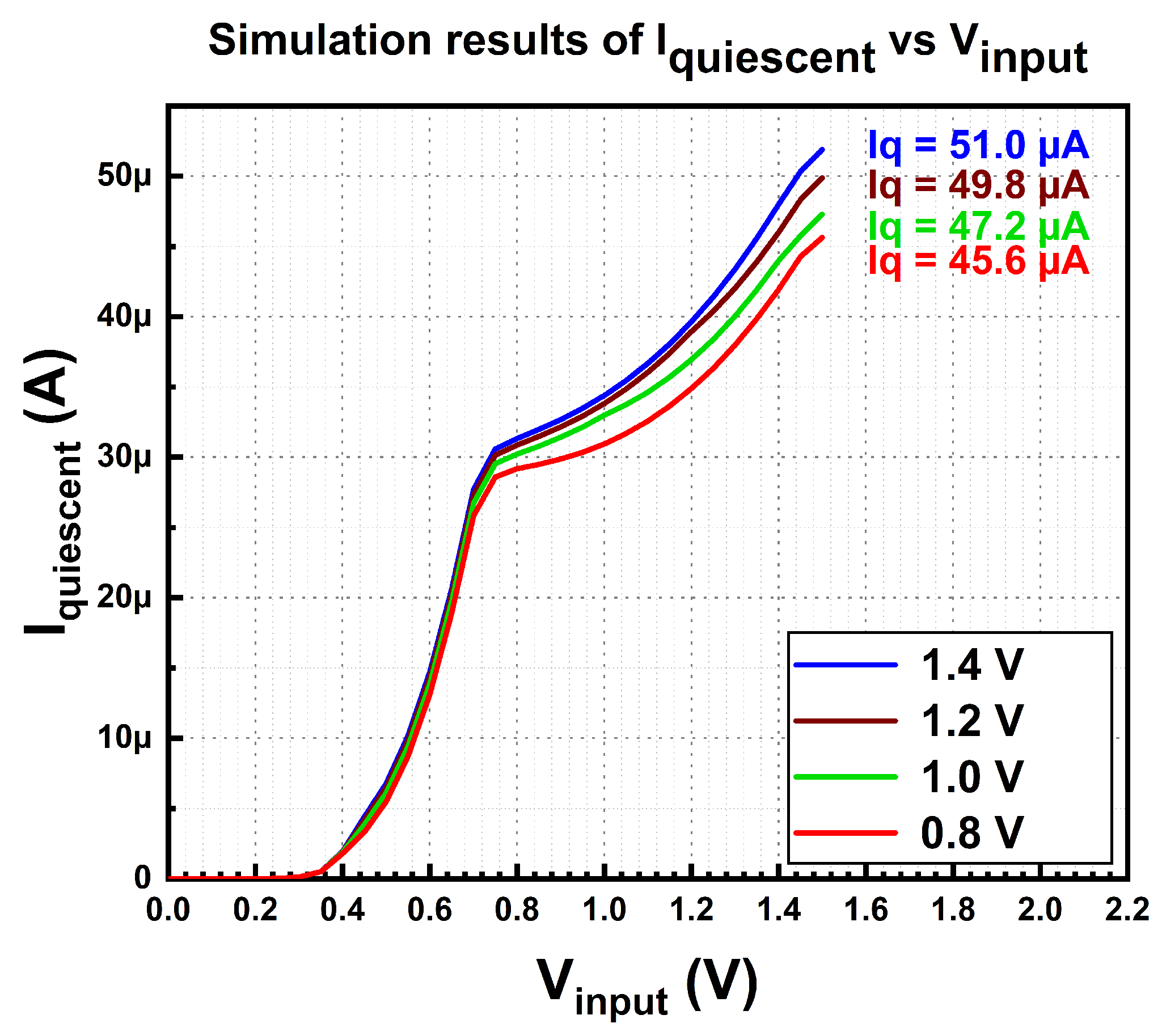
The simulated quiescent current of the MVD-LDO is plotted in
Figure 6.
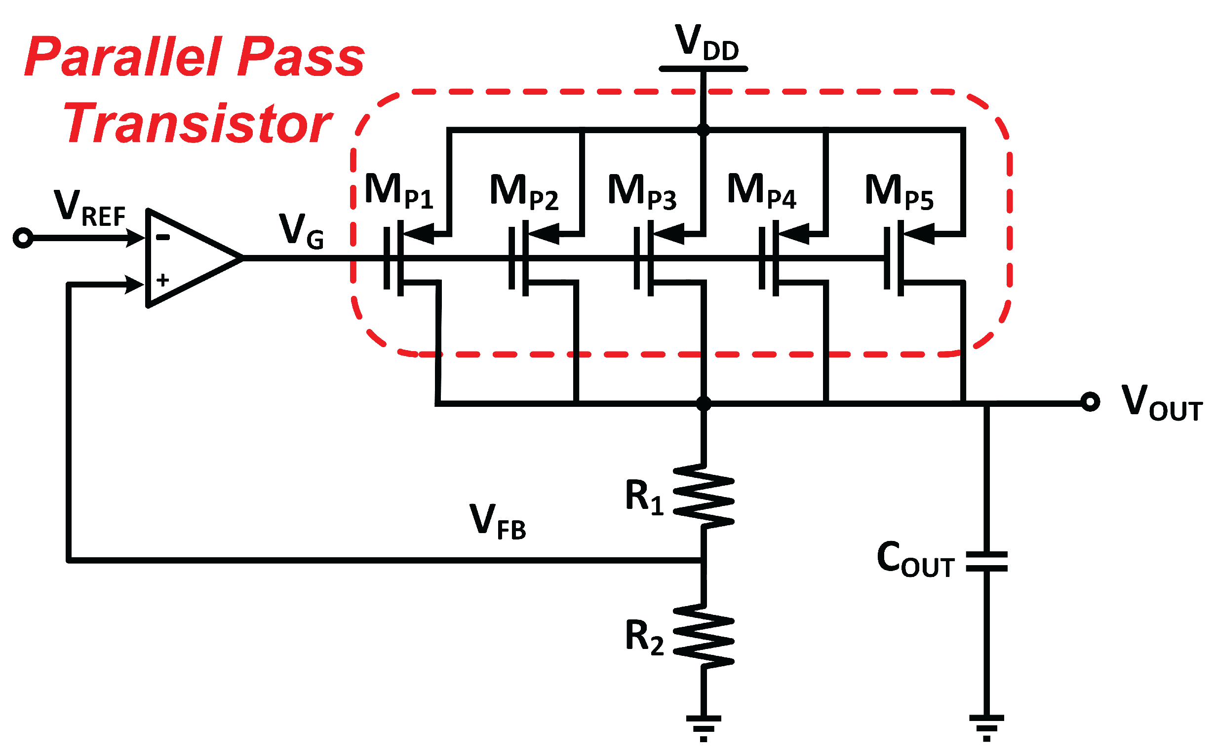
The MVD-LDO is designed to carry 400 mA of load current. To accomplish this, parallel PMOS transistors operating in the saturation region were implemented as pass transistors [
19], as depicted in
Figure 7. The size of the pass transistor is a matter to support the large current. The load current of the LDO is usually determined by the capacity of the pass device.
Smaller pass devices can only support a modest load current, whereas larger devices can support a large current based on the transistor’s capacity. By increasing the size of the transistor to support higher load current, it impacts the size of the chip. In the proposed MVD-LDO, multiple transistors are connected in parallel, while the size of each transistor is significantly smaller. The parallel pass transistor approach increases the capacity of the pass device to accommodate large load currents while keeping the transistor size smaller. The parallel PMOS also significantly reduces the quiescent current. Consequently, LDO’s current efficiency is enhanced.
The load regulation of the MVD-LDO is related to closed-loop DC output resistances, R
out,cl, of the LDO, as illustrated in (5):
where g
mp is the transconductance of the pass transistor, R
out is the output impedance,
is the feedback factor of the amplifier, and A
EA,O is the DC gain of the error amplifier.
To achieve good load regulation, the closed-loop DC output resistance, R
out,cl was designed to be smaller [
20]. Referring to (9), the R
out,cl, reduces when the DC gain of the error amplifier, A
EA,O, increases.
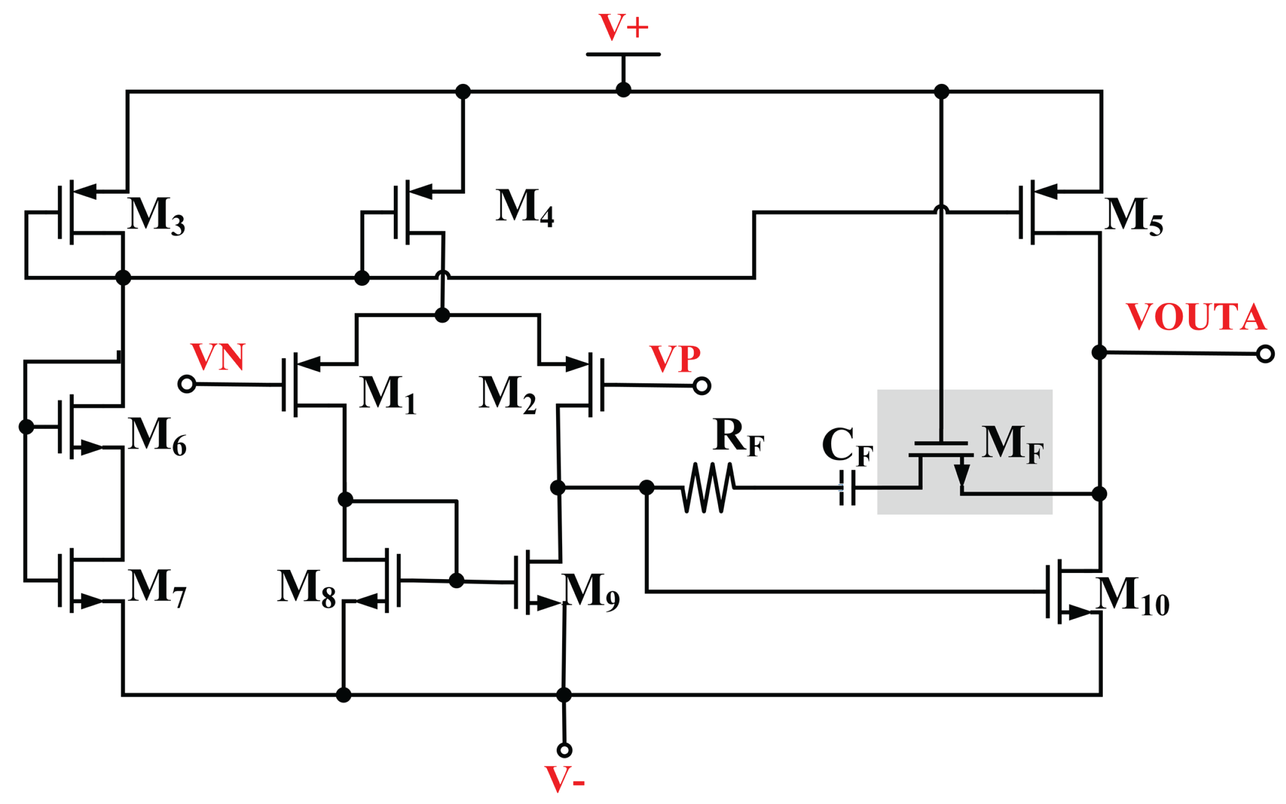
Figure 8 illustrates the high gain op-amp used as error amplifier in the MVD-LDO.
The high gain error amplifier consists of an operational transconductance amplifier as first stage and a common source amplifier as second stage. The common source delivers higher output voltage swing. M
1 and M
2 are the input stage which operates in the saturation region. The equivalent transfer function is given as:
The overall DC gain of the error amplifier is given as:
The MVD-LDO achieves optimum load regulation and transient analysis by boosting the error amplifier’s DC gain. The transient analysis of the LDO is simulated and plotted in
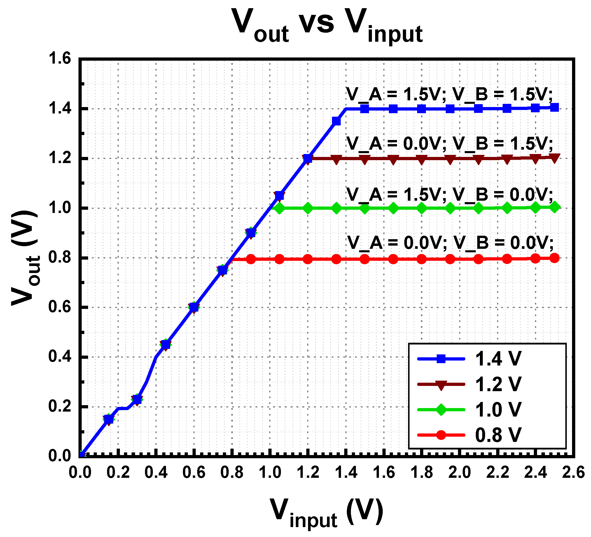
Figure 9.
Based on the transient analysis simulation, the output voltage ripple was obtained. It is evident that without the external capacitor, the output voltage variation is significantly lower.
Figure 10, employed the simulation results of the output voltage ripple for all four outputs during full-load conditions.
5. Measurement Results
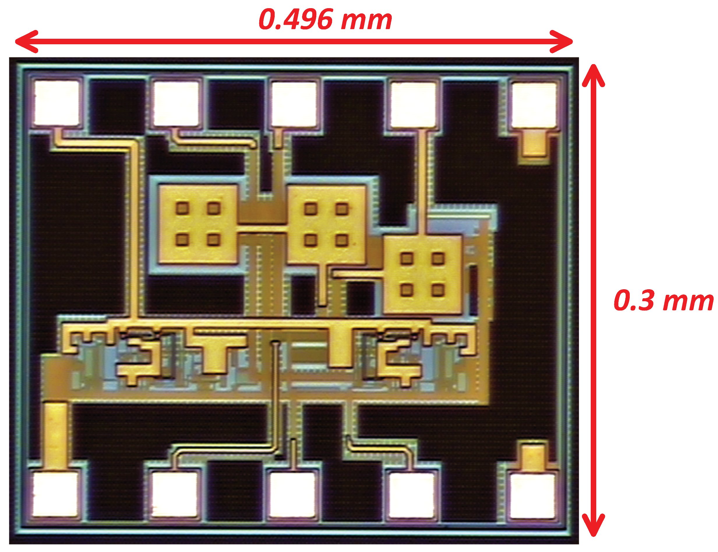
The proposed multi-voltage domain LDO regulator was fabricated using 180 nm CMOS process technology to verify the feasibility of the proposed design topology.
Figure 11 depicts the micrograph of the proposed LDO.
The proposed LDO regulator can support a load current of up to 400 mA without using any external component, especially an off-chip capacitor (C
L).
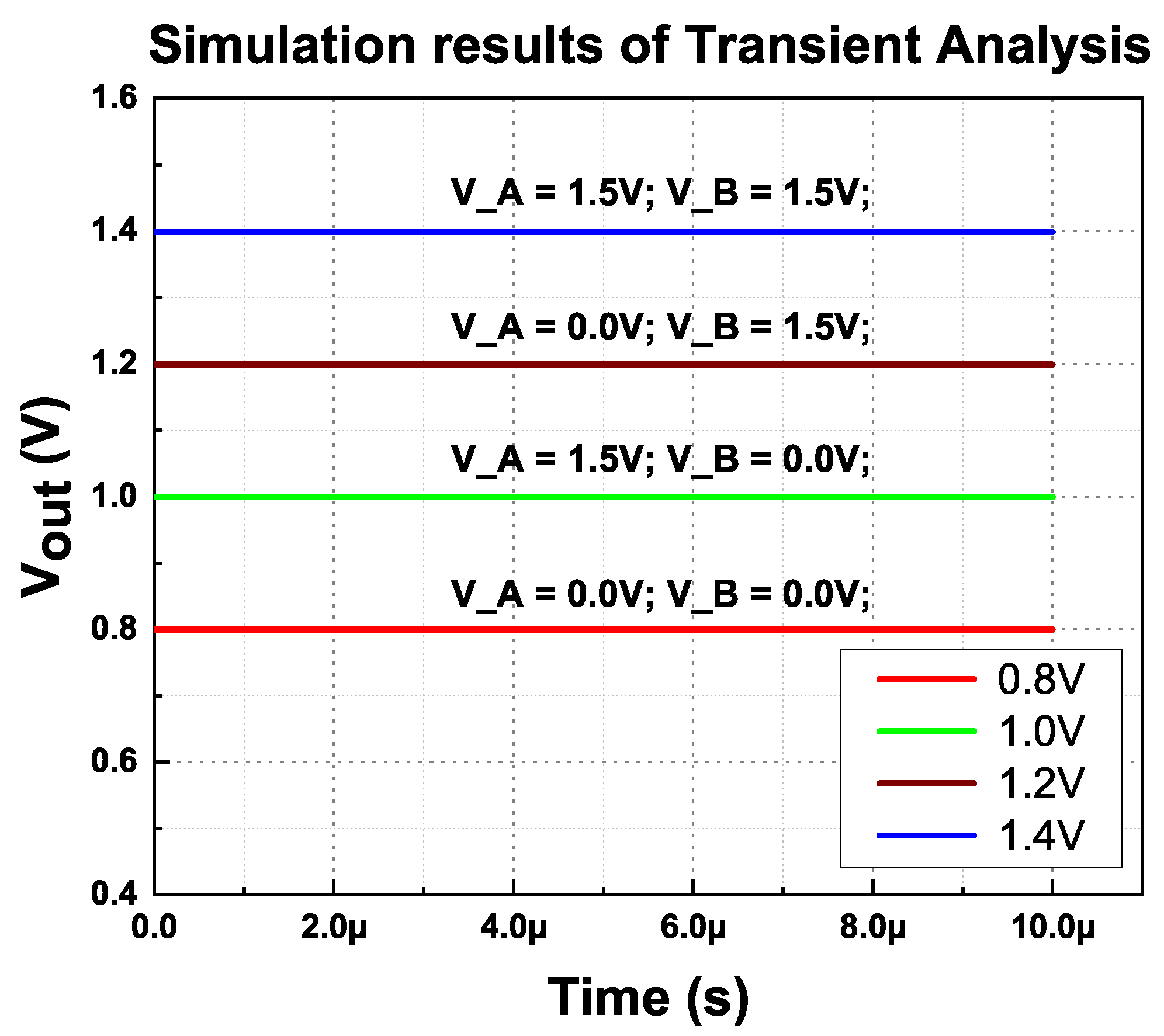
Figure 12 illustrates the measured multi-voltage domain output voltage from 0.8 V to 1.4 V, with different configuration during no load conditions. The test configuration setup with digital logic is presented in
Table 1.
The test configuration setup with digital logic is presented in
Table 1.
Line regulation of LDO computes from the measured result from
Figure 12 when the supply voltage is 1.5 V. For output voltage of 0.8 V, the line regulation is 1.85 mV/V, while for 1.0 V regulated voltage, the line regulation is 2.7 mV/V. Besides this, the line regulation values for output voltages of 1.2 V and 1.4 V are 2.19 mV/V and 3.53 mV/V, respectively.
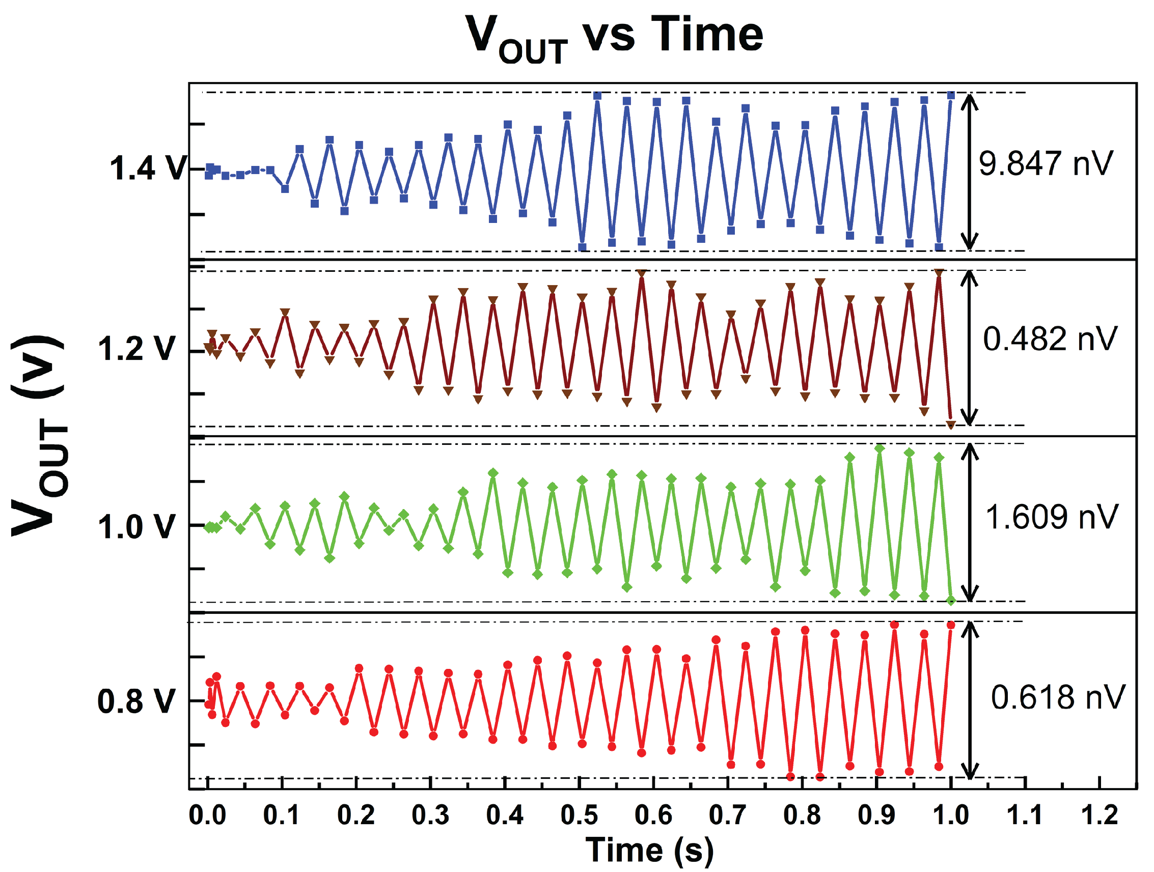
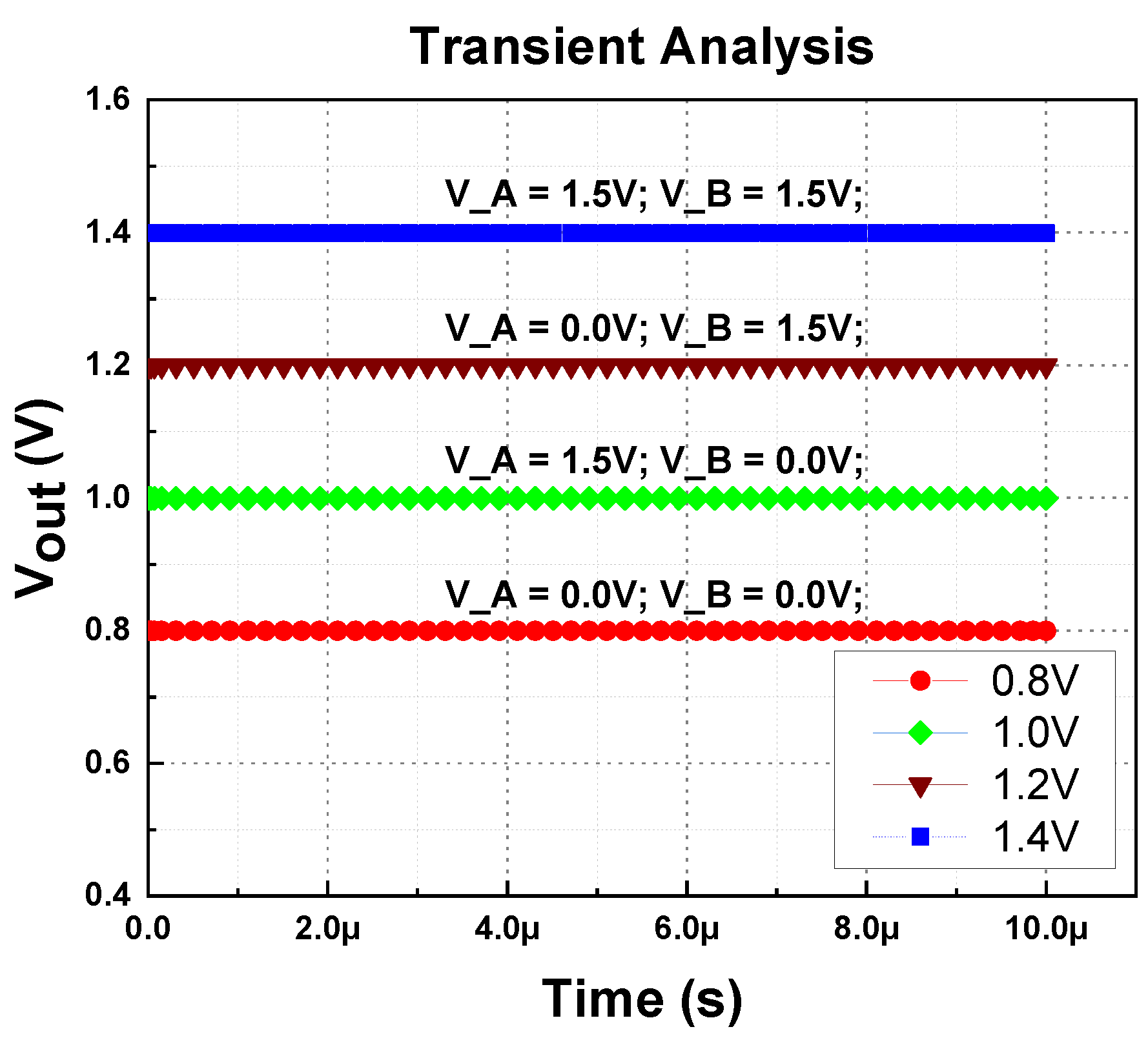
The transient analysis of the measured waveform is shown in
Figure 13. All four regulated output voltages look stable.
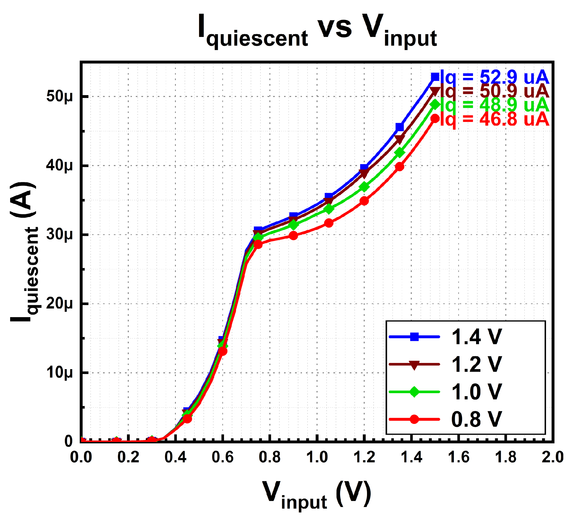
Figure 14 demonstrates the quiescent current of the multi-voltage domain LDO regulator for each test configuration. During this measurement, the regulator connects to zero load. Based on the measured results, the lowest quiescent current is 46.8 µA, while the highest is 52.9 µA with the output voltage of 0.8 V and 1.4 V, respectively. The highest multi-voltage domain output voltage contributes to the largest quiescent current, while otherwise, the relationship is reversed. The results dictate that output voltage is directly proportional to quiescent current. This quiescent current is the total operating current for bandgap reference, differential amplifier, and demultiplexer, which operate during no-load and full-load conditions.
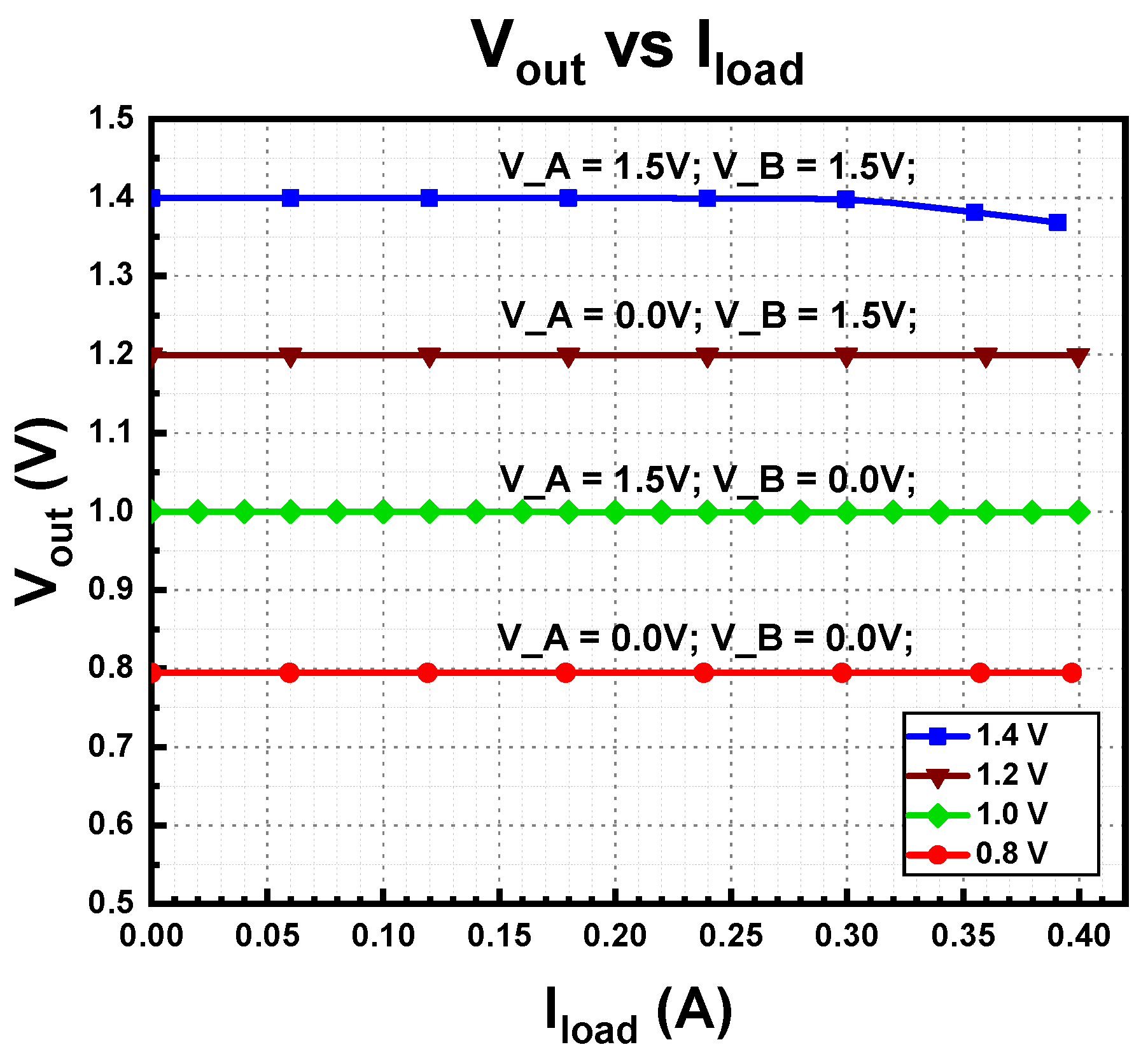
The load regulation on the multi-voltage domains is shown in
Figure 15. The output voltage was measured while varying the load from no-load condition to full-load condition with current step of 20 mA. The load regulation values for multi-voltages of 0.8 V, 1.0 V, 1.2 V, and 1.4 V are 0.0003 mV/mA, 0.000325 mV/mA, 0.0004 mV/mA, and 0.079 mV/mA, respectively. Like line regulation, the load regulation has the smallest load regulation when the lowest multi-voltage domain voltage is highest when the output voltage is huge.
Current efficiency is an important parameter in LDO regulators as the input and output current are close enough. To evaluate the current efficiency of the regulator, the input current and output current were measured during the full-load condition. Based on the measured results, the current efficiency of the regulator for all four output voltages is computed and displayed in
Table 2.
The current efficiency of the MVD-LDO regulator was about 99.98% for all four tested configurations.
Table 3 summarizes the performance of the proposed multi-voltage domain LDO regulator and compares it with other state-of-the-art LDOs.

 ,
, 


