
Synthesis of Er3+:YAG Nanocrystals and Comparative Spectroscopic Analysis with Bulk Counterparts
 , ,
, , 
Abstract
:1. Introduction
2. Materials and Methods
3. Results
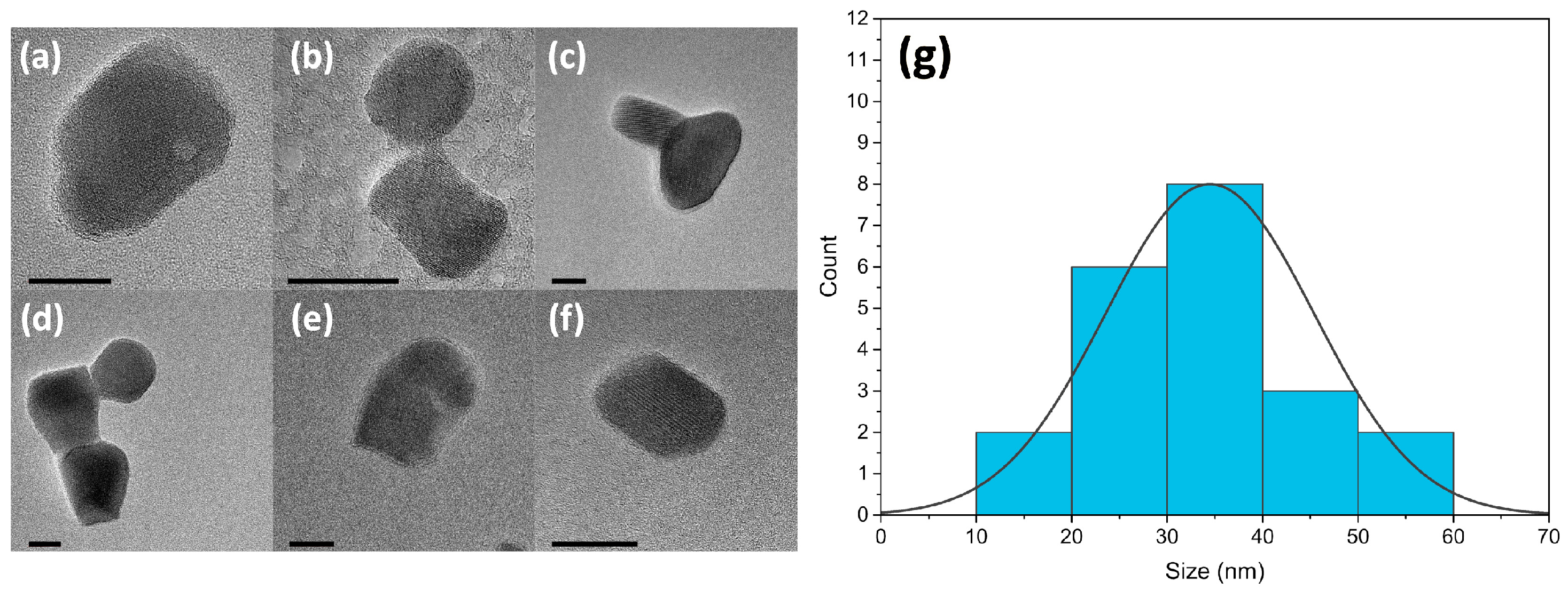
3.1. Morphology
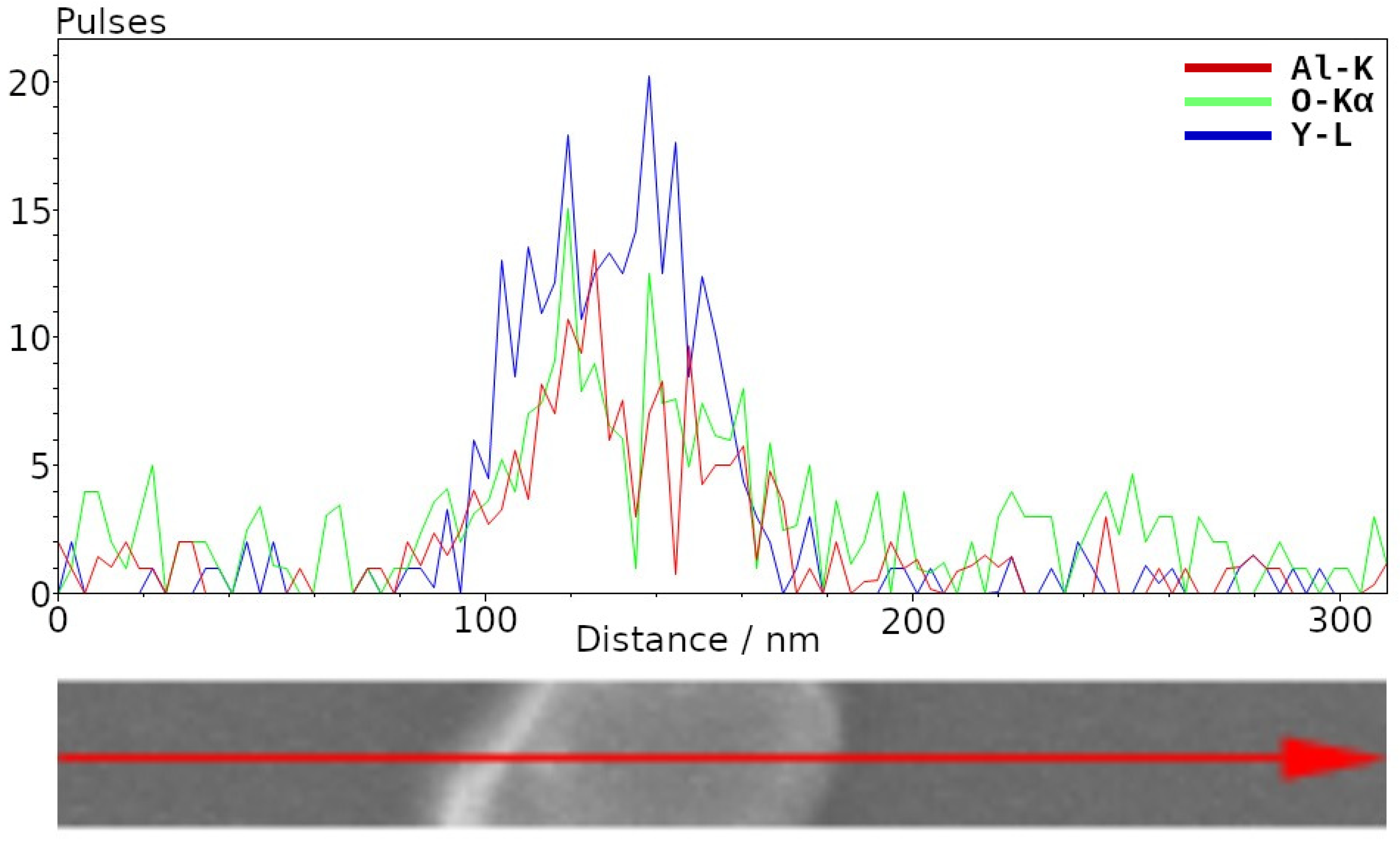
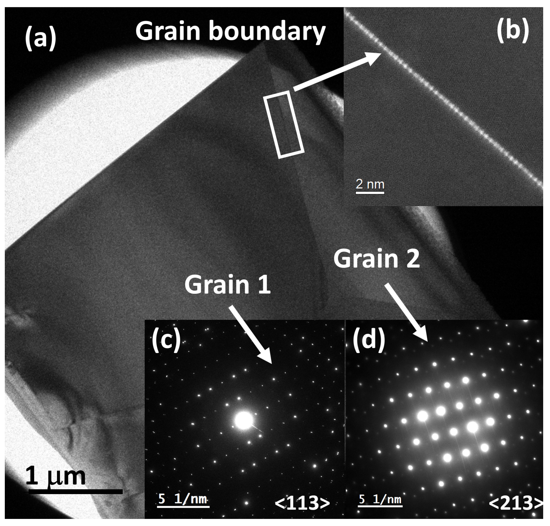
3.2. Microscopy
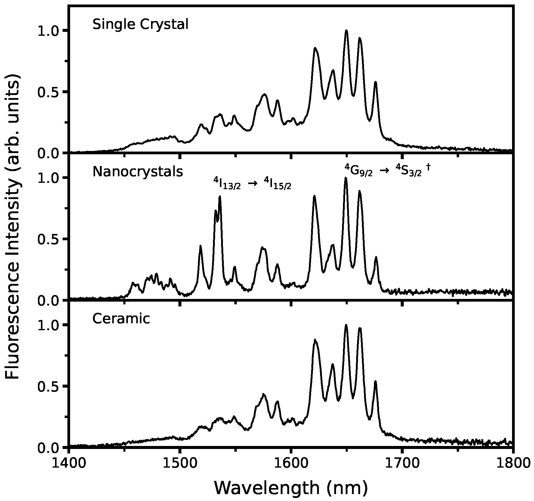
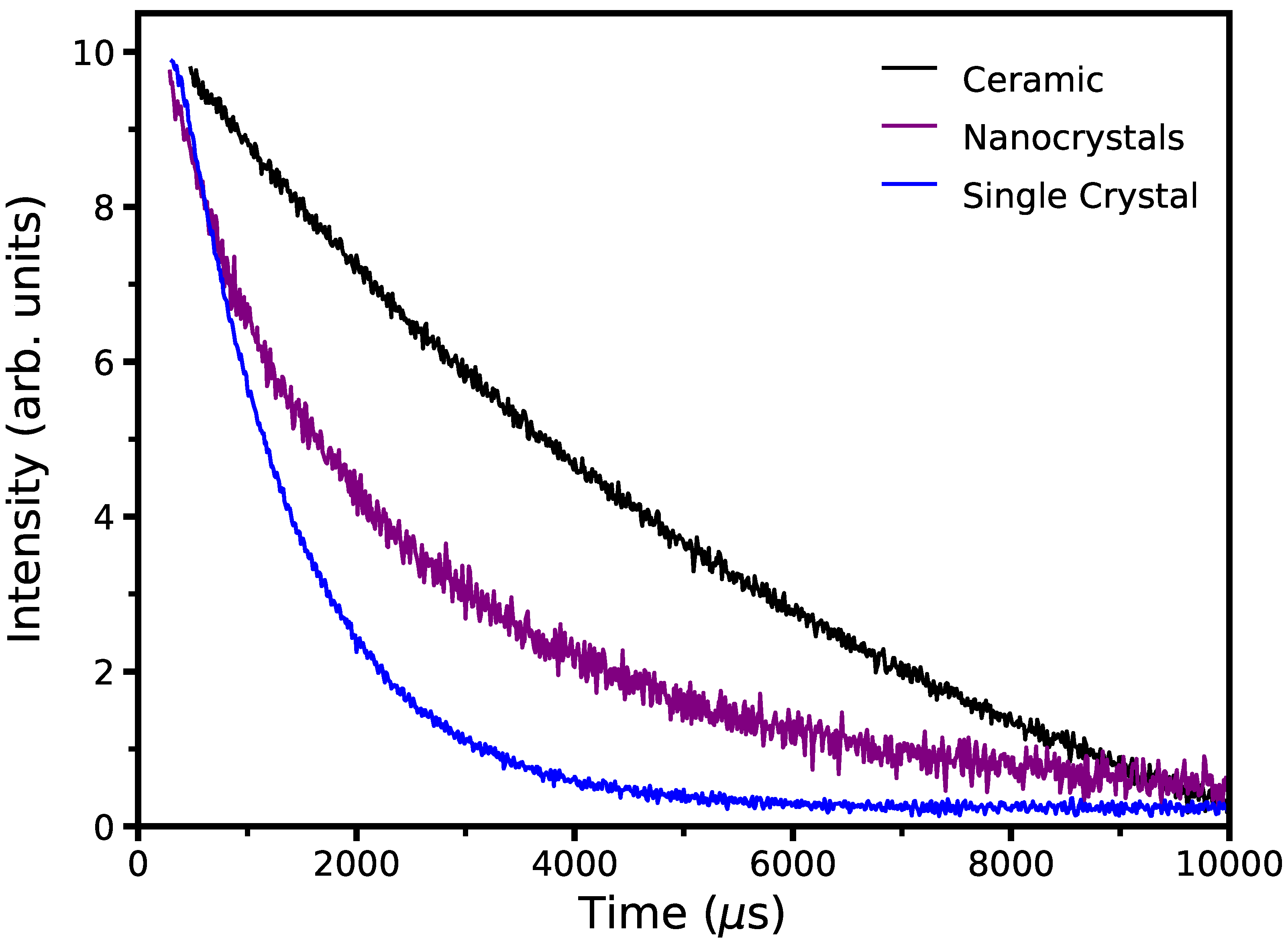
3.3. Spectroscopy
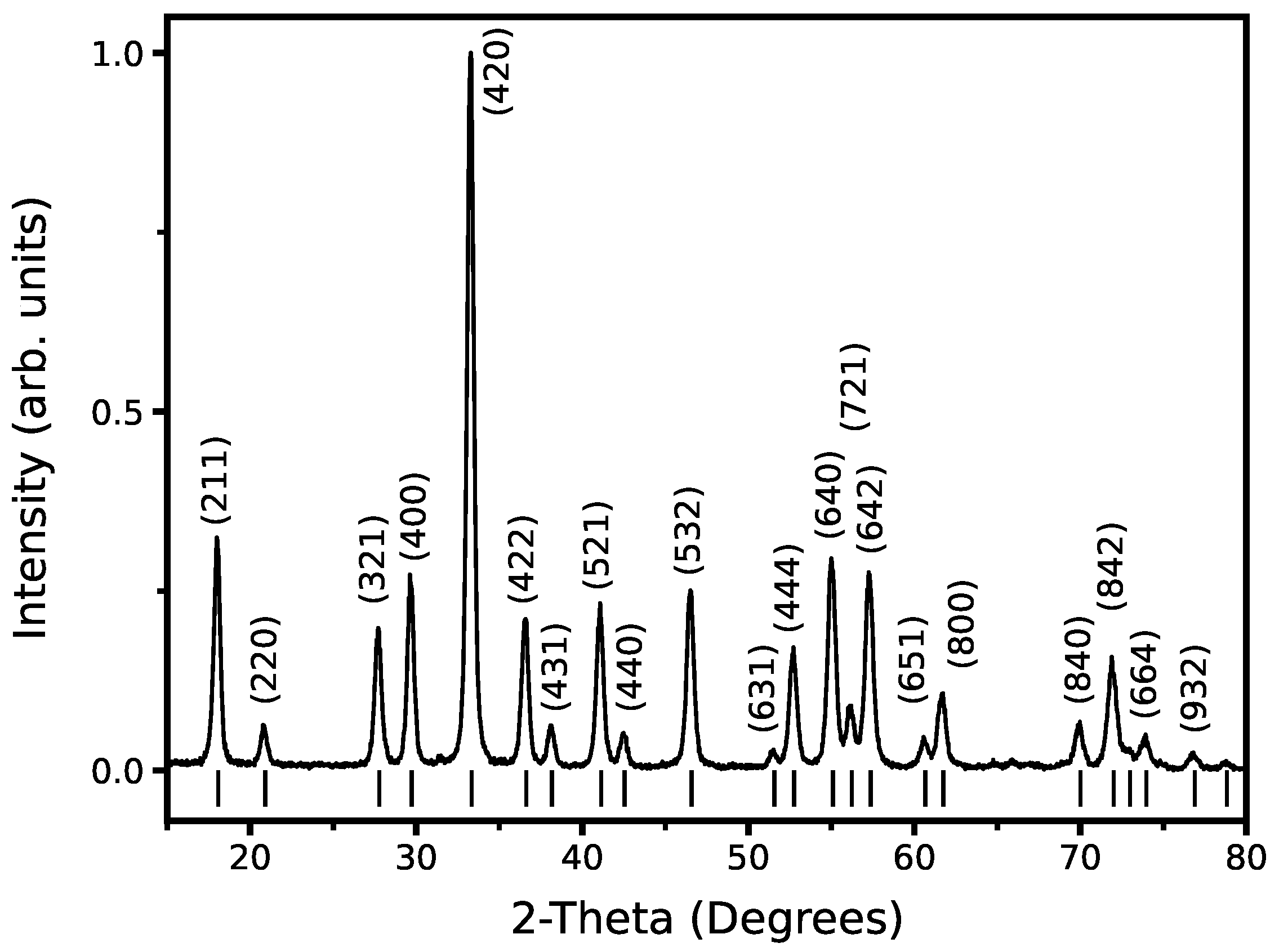
3.4. Crystal Structure
4. Conclusions
Author Contributions
Funding
Data Availability Statement
Acknowledgments
Conflicts of Interest
Abbreviations
| YAG | Yttrium aluminum garnet |
| NIR | Near-infrared |
| RE | Rare-earth |
| XRD | X-Ray diffraction |
| FWHM | Full width at half maximum |
| EDS | Energy-dispersive X-ray spectroscopy |
| STEM | Scanning transmission electron microscope |
| TEM | Transmission electron microscopy |
| HRTEM | High-resolution transmission electron microscopy |
| PTI | Photon technology international |
| FIB | Focused ion beam |
| SAED | Selected area electron diffraction |
| PED | Precession electron diffraction |
| HAADF | High-angle annular dark field |
| Cs | Spherical aberration correction |
References
- Koechner, W. Solid-State Laser Engineering; Springer Series in Optical Sciences; Springer: New York, NY, USA, 2006; Volume 1. [Google Scholar] [CrossRef]
- Taccheo, S.; Laporta, P.; Longhi, S.; Svelto, O.; Svelto, C. Diode-pumped bulk erbium-ytterbium lasers. Appl. Phys. B 1996, 63, 425–436. [Google Scholar] [CrossRef]
- Schweizer, T.; Jensen, T.; Heumann, E.; Huber, G. Spectroscopic properties and diode pumped 1.6 μm laser performance in Yb-codoped Er:Y3Al5O12 and Er:Y2SiO5. Opt. Commun. 1995, 118, 557–561. [Google Scholar] [CrossRef]
- Qin, X.; Yang, H.; Shen, D.; Chen, H.; Zhou, G.; Luo, D.; Zhang, J.; Wang, S.; Ma, J.; Tang, D. Fabrication and Optical Properties of Highly Transparent Er:YAG Polycrystalline Ceramics for Eye-Safe Solid-State Lasers. Int. J. Appl. Ceram. Technol. 2013, 10, 123–128. [Google Scholar] [CrossRef]
- Wang, P.; Dawes, J.M.; Burns, P.; Piper, J.A.; Zhang, H.; Zhu, L.; Meng, X. Diode-pumped cw tunable Er3+:Yb3+:YCOB laser at 1.5–1.6 μm. Opt. Mater. 2002, 19, 383–387. [Google Scholar] [CrossRef]
- Dieke, G.H. Spectra and Energy Levels of Rare Earth Ions in Crystals. Am. J. Phys. 1970, 38, 399–400. [Google Scholar] [CrossRef]
- Greskovich, C.; Chernoch, J.P. Polycrystalline ceramic lasers. J. Appl. Phys. 1973, 44, 4599–4606. [Google Scholar] [CrossRef]
- Sekita, M.; Haneda, H.; Shirasaki, S.; Yanagitani, T. Optical spectra of undoped and rare-earth-(=Pr, Nd, Eu, and Er) doped transparent ceramic Y3Al5O12. J. Appl. Phys. 1991, 69, 3709–3718. [Google Scholar] [CrossRef]
- Kumar, G.A.; Jianren, L.; Kaminskii, A.A.; Ueda, K.I.; Yagi, H.; Yanagitani, T.; Unnikrishnan, N.V. Spectroscopic and stimulated emission Characteristics of Nd3+ in transparent YAG ceramics. IEEE J. Quantum Electron. 2004, 40, 747–758. [Google Scholar] [CrossRef]
- Lupei, V.; Lupei, A.; Ikesue, A. Transparent polycrystalline ceramic laser materials. Opt. Mater. 2008, 30, 1781–1786. [Google Scholar] [CrossRef]
- Gruber, J.B.; Nijjar, A.S.; Sardar, D.K.; Yow, R.M.; Russell, C.C.; Allik, T.H.; Zandi, B. Spectral analysis and energy-level structure of Er3+(4f11) in polycrystalline ceramic garnet Y3Al5O12. J. Appl. Phys. 2005, 97, 063519. [Google Scholar] [CrossRef]
- Ikesue, A.; Kinoshita, T.; Kamata, K.; Yoshida, K. Fabrication and optical properties of high-performance polycrystalline Nd:YAG ceramics for solid-state lasers. J. Am. Ceram. Soc. 1995, 78, 1033–1040. [Google Scholar] [CrossRef]
- Lu, J.; Prabhu, M.; Xu, J.; Ueda, K.i.; Yagi, H.; Yanagitani, T.; Kaminskii, A.A. Highly efficient 2% Nd: Yttrium aluminum garnet ceramic laser. Appl. Phys. Lett. 2000, 77, 3707–3709. [Google Scholar] [CrossRef]
- Lu, J.; Ueda, K.i.; Yagi, H.; Yanagitani, T.; Akiyama, Y.; Kaminskii, A.A. Neodymium doped yttrium aluminum garnet (Y3Al5O12) nanocrystalline ceramics—A new generation of solid state laser and optical materials. J. Alloys Compd. 2002, 341, 220–225. [Google Scholar] [CrossRef]
- Shi, W.Q.; Bass, M.; Birnbaum, M. Effects of energy transfer among Er3+ ions on the fluorescence decay and lasing properties of heavily doped Er:Y3Al5O12. J. Opt. Soc. Am. B 1990, 7, 1456–1462. [Google Scholar] [CrossRef]
- Zhekov, V.I. Cooperative process in Y3Al5O12:Er3+ crystals. Sov. J. Quantum Electron. 1986, 16, 274–276. [Google Scholar] [CrossRef]
- Sardar, D.K.; Russell, C.C.; Gruber, J.B.; Allik, T.H. Absorption intensities and emission cross sections of principal intermanifold and inter-Stark transitions of Er3+ (4f11) in polycrystalline ceramic garnet Y3Al5O12. J. Appl. Phys. 2005, 97, 123501. [Google Scholar] [CrossRef] [Green Version]
- Saladino, M.L.; Caponetti, E.; Martino, D.C.; Enzo, S.; Ibba, G. Effect of the dopant selection (Er, Eu, Nd or Ce) and its quantity on the formation of yttrium aluminum garnet nanopowders. Opt. Mater. 2008, 31, 261–267. [Google Scholar] [CrossRef]
- Nishi, M.; Tanabe, S.; Inoue, M.; Takahashi, M.; Fujita, K.; Hirao, K. Optical-telecommunication-band fluorescence properties of Er3+-doped YAG nanocrystals synthesized by glycothermal method. Opt. Mater. 2005, 27, 655–662. [Google Scholar] [CrossRef]
- Rodríguez, R.A.; Tobar, E.H.; la Rosa, E.D.; Díaz-Torres, L.A.; Salas, P.; Torres, A.; Felix, M.V.; Castañeda-Contreras, J.; Yacaman, M.J. Structural and photoluminescence characterization of nanocrystalline YAG: Er3+ prepared with the addition of PVA and UREA. Proc. SPIE 2007, 6639, 66390K. [Google Scholar] [CrossRef]
- Quarles, G.J.; VLOC, 7826 Photonics Drive, New Port Richey, FL 34655, USA. Personal Communication, 2020.
- Kokta, M.R.; Bicron Crystal Products, 750 South 32nd Street, Washougal, WA 98671, USA. Personal Communication, 2020.
- Dai, P.; Ji, C.; Shen, L.; Qian, Q.; Guo, G.; Zhang, X.; Bao, N. Photoluminescence properties of YAG:Ce3+,Pr3+ nano-sized phosphors synthesized by a modified co-precipitation method. J. Rare Earths 2017, 35, 341–346. [Google Scholar] [CrossRef]
- Pokhrel, M.; Kumar, G.A.; Ma, C.G.; Brik, M.G.; Langloss, B.W.; Stanton, I.N.; Therien, M.J.; Sardar, D.K.; Mao, Y. Electronic and optical properties of Er-doped Y2O2S phosphors. J. Mater. Chem. C 2015, 3, 11486–11496. [Google Scholar] [CrossRef]
- Saltmarsh, N.; Kumar, G.; Kailasnath, M.; Shenoy, V.; Santhosh, C.; Sardar, D. Spectroscopic characterizations of Er doped LaPO4 submicron phosphors prepared by homogeneous precipitation method. Opt. Mater. 2016, 53, 24–29. [Google Scholar] [CrossRef] [Green Version]
- Mimun, L.C.; Ajithkumar, G.; Rightsell, C.; Langloss, B.W.; Therien, M.J.; Sardar, D.K. Synthesis and characterization of Na(Gd0.5Lu0.5)F4: Nd3+, a core-shell free multifunctional contrast agent. J. Alloys Compd. 2017, 695, 280–285. [Google Scholar] [CrossRef] [PubMed] [Green Version]
- Gayathri, K.; Kumar, G.A.; Manrique, S.I.R.; Santhosh, C.; Sardar, D.K. Optical characterization of infrared emitting Nd3+ doped hydroxyapatite nanoparticles prepared by hydrothermal method. J. Lumin. 2017, 185, 180–186. [Google Scholar] [CrossRef] [Green Version]
- Yoder, H.; Keith, M. Complete substitution of aluminum for silicon: The system 3MnO·Al2O3·3SiO2–3Y2O3·5Al2O3. Am. Mineral. J. Earth Planet. Mater. 1951, 36, 519–533. [Google Scholar]
- Jüstel, T.; Nikol, H.; Ronda, C. New Developments in the Field of Luminescent Materials for Lighting and Displays. Angew. Chem. Int. Ed. 1998, 37, 3084–3103. [Google Scholar] [CrossRef]
- Ortega, E.; Sanchez, D.; Sardar, D.; Arellano, J.; Ponce, A. Microstructural Analysis of Polycrystalline Er:YAG using Automated Crystal Orientation Mapping. Proc. Microsc. Microanal. 2018, 24, 218–219. [Google Scholar] [CrossRef] [Green Version]
- Pennycook, S. Z-contrast stem for materials science. Ultramicroscopy 1989, 30, 58–69. [Google Scholar] [CrossRef]
- Pokhrel, M.; Kumar, G.A.; Samuel, P.; Ueda, K.I.; Yanagitani, T.; Yagi, H.; Sardar, D.K. Infrared and upconversion spectroscopic studies of high Er3+ content transparent YAG ceramic. Opt. Mater. Express 2011, 1, 1272–1285. [Google Scholar] [CrossRef] [Green Version]
- Pokhrel, M.; Ray, N.; Kumar, G.A.; Sardar, D.K. Comparative studies of the spectroscopic properties of Nd3+: YAG nanocrystals, transparent ceramic and single-crystal. Opt. Mater. Express 2012, 2, 235–249. [Google Scholar] [CrossRef]


Disclaimer/Publisher’s Note: The statements, opinions and data contained in all publications are solely those of the individual author(s) and contributor(s) and not of MDPI and/or the editor(s). MDPI and/or the editor(s) disclaim responsibility for any injury to people or property resulting from any ideas, methods, instructions or products referred to in the content. |
© 2023 by the authors. Licensee MDPI, Basel, Switzerland. This article is an open access article distributed under the terms and conditions of the Creative Commons Attribution (CC BY) license (https://creativecommons.org/licenses/by/4.0/).
Share and Cite
Rightsell, C.; Sanchez, D.; Escudero, J.; Ortega, E.; Ajithkumar, G.; Sardar, D.; Ponce, A. Synthesis of Er3+:YAG Nanocrystals and Comparative Spectroscopic Analysis with Bulk Counterparts. Micromachines 2023, 14, 255. https://doi.org/10.3390/mi14020255
Rightsell C, Sanchez D, Escudero J, Ortega E, Ajithkumar G, Sardar D, Ponce A. Synthesis of Er3+:YAG Nanocrystals and Comparative Spectroscopic Analysis with Bulk Counterparts. Micromachines. 2023; 14(2):255. https://doi.org/10.3390/mi14020255
Chicago/Turabian StyleRightsell, Chris, David Sanchez, José Escudero, Eduardo Ortega, Gangadharan Ajithkumar, Dhiraj Sardar, and Arturo Ponce. 2023. "Synthesis of Er3+:YAG Nanocrystals and Comparative Spectroscopic Analysis with Bulk Counterparts" Micromachines 14, no. 2: 255. https://doi.org/10.3390/mi14020255