
Development of Heterojunction c-Si/a-Si1−xCx:H PIN Light-Emitting Diodes
 , ,
, ,  , and
, and
Abstract
:1. Introduction
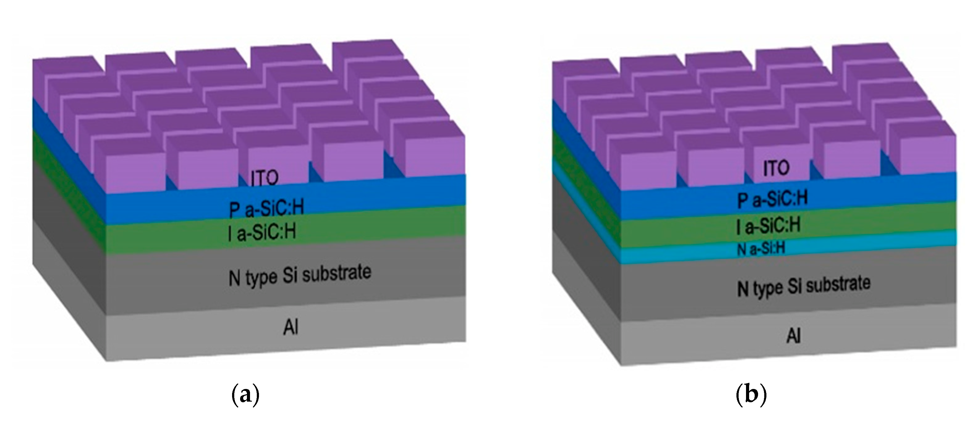
2. Experimental Details
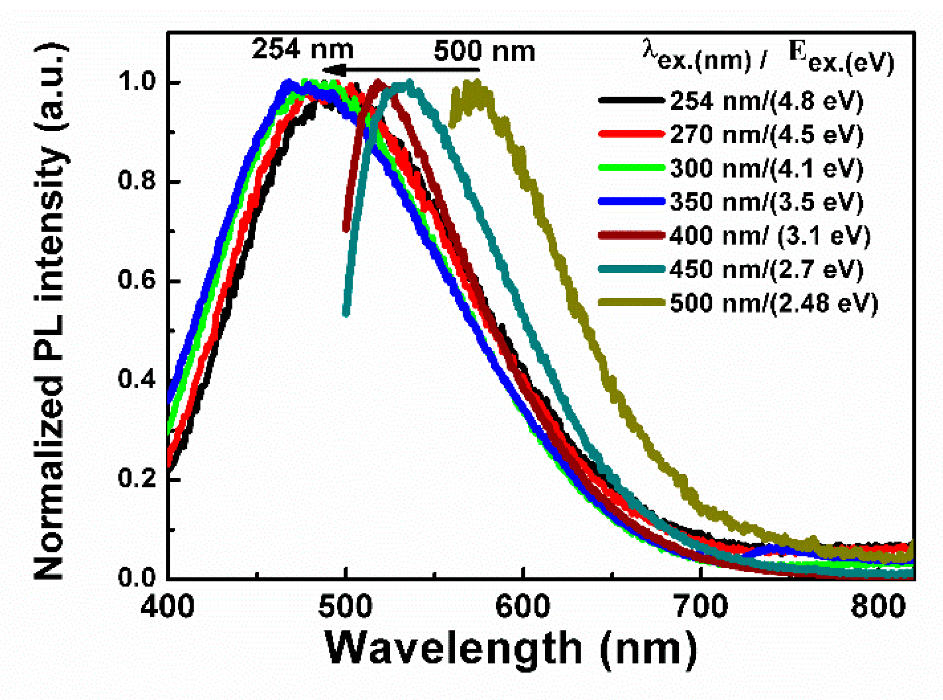
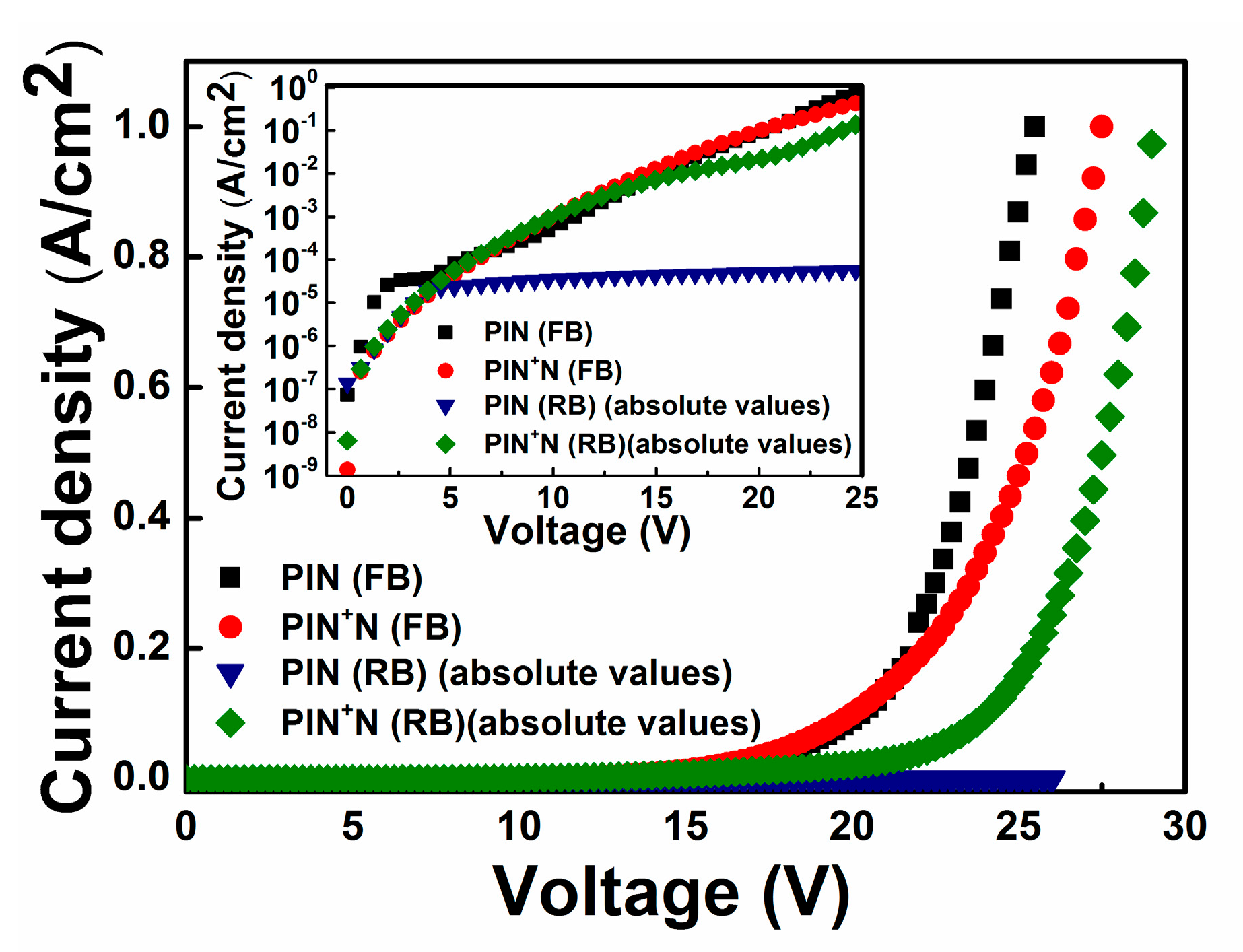
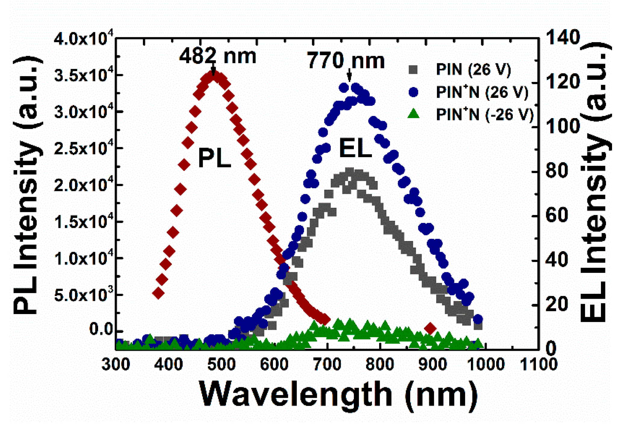
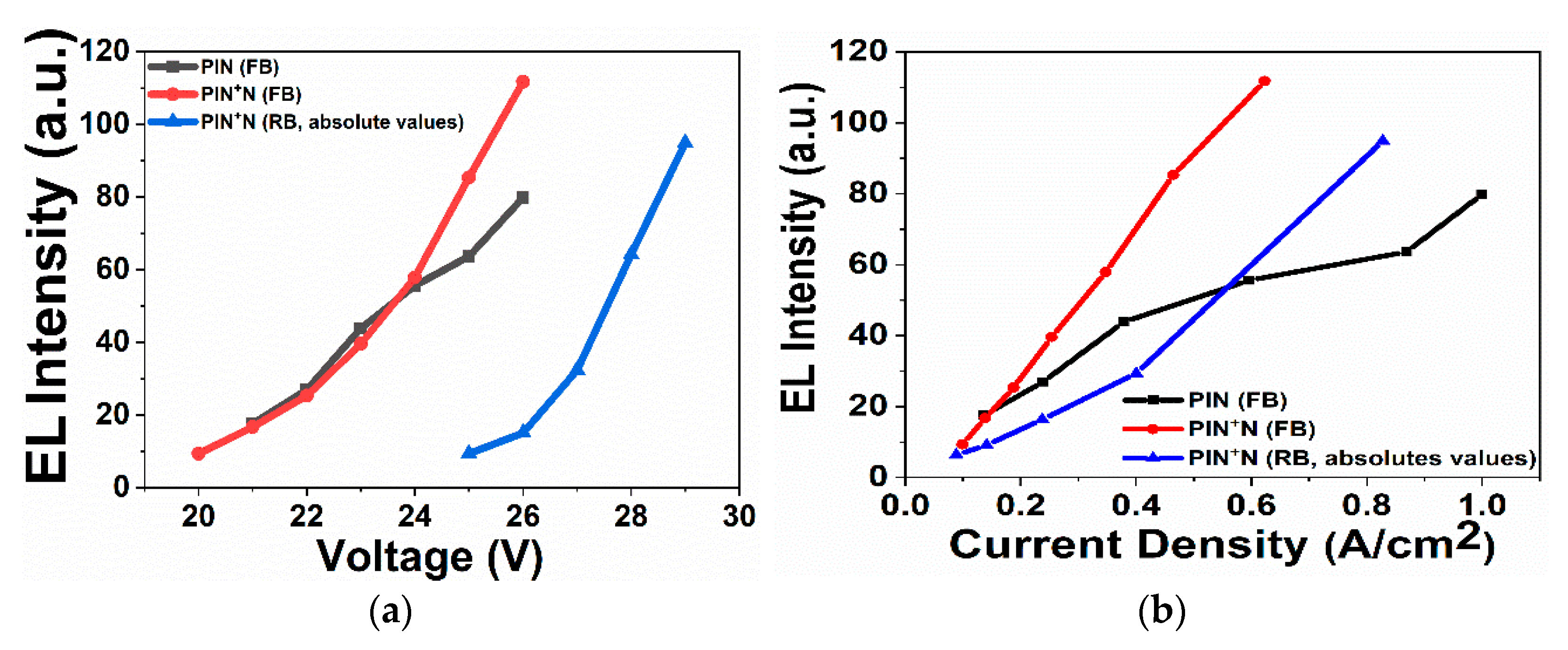
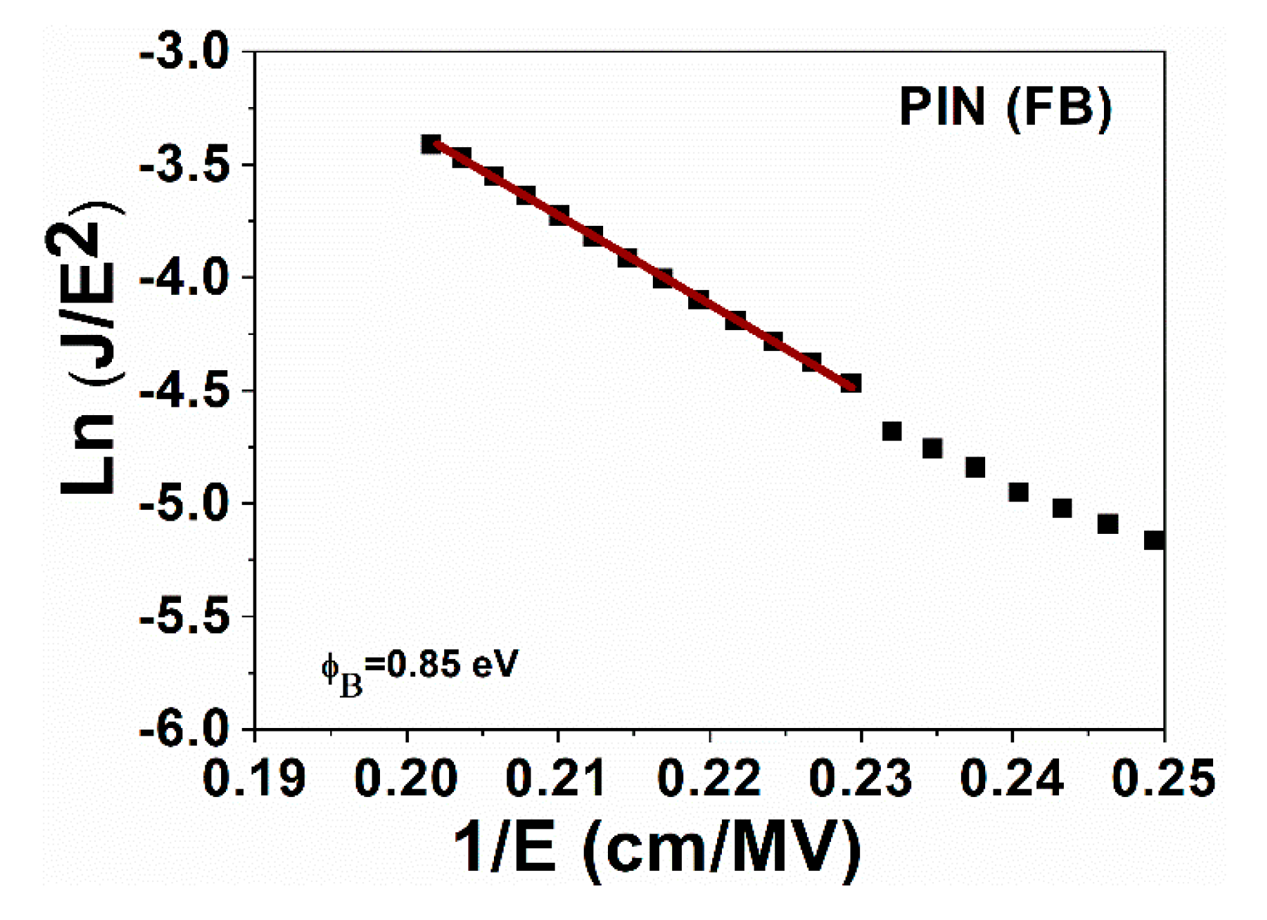
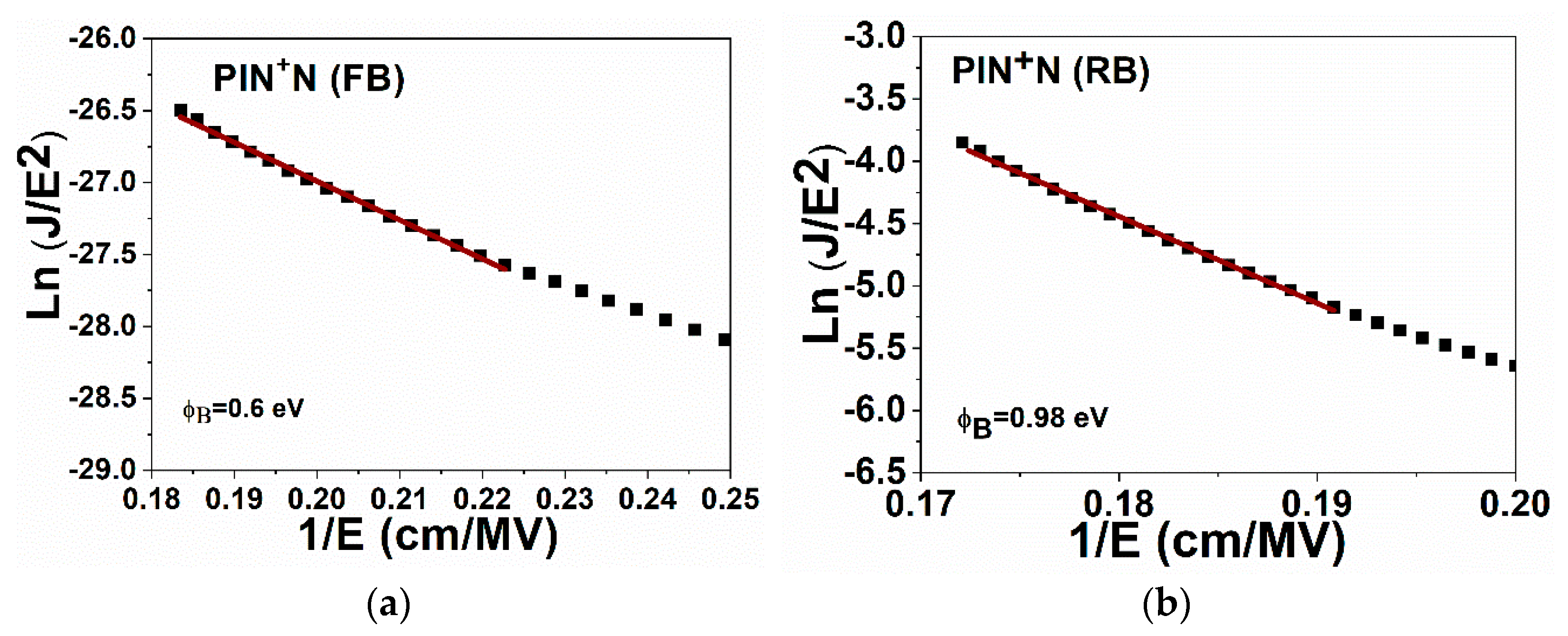
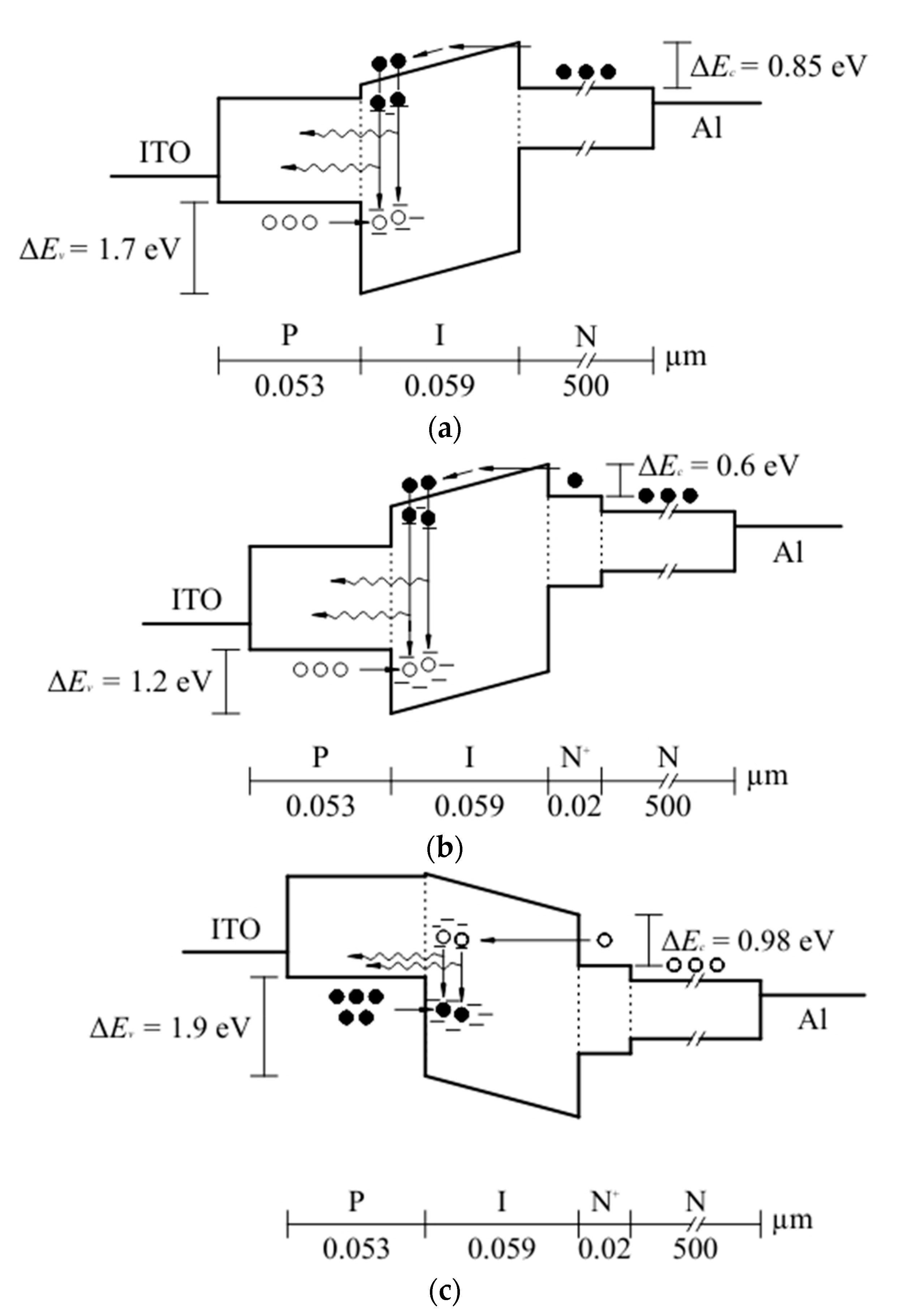
3. Results and Discussion
4. Conclusions
Author Contributions
Funding
Data Availability Statement
Acknowledgments
Conflicts of Interest
References
- Huh, C.; Kim, K.-H.; Kim, B.K.; Kim, W.; Ko, H.; Choi, C.-J.; Sung, G.Y. Enhancement in Light Emission Efficiency of a Silicon Nanocrystal Light-Emitting Diode by Multiple-Luminescent Structures. Adv. Mater. 2010, 22, 5058–5062. [Google Scholar] [CrossRef] [PubMed]
- Anderson, P.W. Model for the Electronic Structure of Amorphous Semiconductors. Phys. Rev. Lett. 1975, 34, 953–955. [Google Scholar] [CrossRef]
- Kanicki, J. Amorphous and Microcrystalline Silicon Carbide Alloy Light Emitting Diodes: Physics and Properties; Artech House: Norwood, MA, USA, 1991; pp. 195–239. [Google Scholar]
- Giorgis, F.; Mandracci, P.; Negro, L.D.; Mazzoleni, C.; Pavesi, L. Optical absorption and luminescence properties of wide-band gap amorphous silicon based alloys. J. Non Cryst. Solids. 2000, 266–269, 588–592. [Google Scholar] [CrossRef]
- Chen, X.Y.; Lu, Y.F.; Tang, L.J.; Wu, Y.H.; Cho, B.J.; Xu, X.J.; Dong, J.R.; Song, W.D. Annealing and oxidation of silicon oxide films prepared by plasma-enhanced chemical vapor deposition. J. Appl. Phys. 2005, 97, 014913. [Google Scholar] [CrossRef] [Green Version]
- Huh, C.; Kim, T.-Y.; Ahn, C.-G.; Kim, B.K. Strong visible electroluminescence from silicon nanocrystals embedded in a silicon carbide film. Appl. Phys. Lett. 2015, 106, 211103. [Google Scholar] [CrossRef]
- Demichelis, F.; Pirri, C.F. Hydrogenated Amorphous Silicon Based Alloy: A-Si1-xCx: H. In Solid State Phenomena; Trans Tech Publications Ltd.: Stafa/Zurich, Switzerland, 1995; Volume 44, pp. 385–424. [Google Scholar]
- Rahman, M.M.; Yang, C.Y.; Sugiarto, D.; Byrne, A.S.; Ju, M.; Tran, K.; Lui, K.H. Properties and device applications of hydrogenated amorphous silicon carbide films. J. Appl. Phys. 1990, 67, 7065–7070. [Google Scholar] [CrossRef] [Green Version]
- Engemann, D.; Fischer, R.; Knecht, J. Photoluminiscence in the amorphous system SixC1-x. Appl. Phys. Lett. 1978, 32, 567–569. [Google Scholar] [CrossRef]
- Munekata, H.; Kukimoto, H. Electroluminescence in hydrogenated amorphous silicon-carbon alloy. Appl. Phys. Lett. 1983, 42, 432–434. [Google Scholar] [CrossRef]
- Kruangam, D.; Endo, T.; Okamoto, W.; Hamakawa, Y. Visible-light injection-electroluminescent a-SiC/pin diode. Jpn. J. Appl. Phys. 1985, 24, L806. [Google Scholar] [CrossRef]
- Hamakawa, Y.; Kruangam, D.; Deguchi, M.; Hattori, Y.; Toyama, T.; Okamoto, H. Visible light thin film led made of a-sic pin junction. Appl. Surf. Sci. 1988, 33, 1142–1150. [Google Scholar] [CrossRef]
- Kruangam, D.; Deguchi, M.; Toyama, T.; Okamoto, H.; Hamakawa, Y. Carrier injection mechanism in an a-SiC p-i-n junction thin-film led. IEEE Trans. Electron Devices. 1988, 35, 957–965. [Google Scholar] [CrossRef]
- Paasche, S.M.; Toyama, T.; Okamoto, H.; Hamakawa, Y. Amorphous-SiC thin-film pin light-emitting diode using amorphous-SiN hot-carrier tunneling injection layers. IEEE Trans. Electron Devices. 1989, 36, 2895–2902. [Google Scholar] [CrossRef]
- Jen, T.S.; Pan, J.W.; Shin, N.F.; Tsay, W.C.; Chang, J.W.H. Hydrogenated amorphous silicon carbide pin thin-film light-emitting diodes with barrier layers inserted at pi interface. Jpn. J. Appl. Phys. 1994, 33, 827. [Google Scholar] [CrossRef]
- Alvarez, F.; Fragnito, H.L.; Chambouleyron, I. Electroluminescence from amorphous silicon carbide heterojunctions under reverse biased conditions. J. Appl. Phys. 1988, 63, 244–246. [Google Scholar] [CrossRef]
- Rui, Y.; Li, S.; Xu, J.; Cao, Y.; Li, W.; Chen, K. Comparative study of electroluminescence from annealed amorphous SiC single layer and amorphous Si/SiC multilayers. J. Non-Cryst. Solids. 2012, 358, 2114–2117. [Google Scholar] [CrossRef]
- Chen, X.; Guo, X.; Wu, W.; Fan, J. Quasi-White Light-Emitting Devices Based on SiC Quantum Dots. Phys. Status Solidi Rapid Res. Lett. 2018, 12, 1800171. [Google Scholar] [CrossRef]
- Oliveira, A.; Carreño, M. Post thermal annealing crystallization and reactive ion etching of SiC films produced by PECVD. J Non Cryst. Solids 2006, 352, 1392–1397. [Google Scholar] [CrossRef]
- Meneses, M.; Moreno, M.; Morales, A.; Torres, A.; Rosales, P.; Vivaldo, I. Study and optimization of the photoluminescence of amorphous silicon carbide thin films. MRS Adv. 2018, 3, 3905–3916. [Google Scholar] [CrossRef]
- Velandia-Caballero, O.J. Study and Solar Cells Development Based on Crystalline Silicon/Doped Amorphous Silicon Structures. Master’s Thesis, National Institute of Astrophysics, Optics and Electronics, Puebla, Mexico, January 2018. [Google Scholar]
- Shin, N.-F.; Chen, J.-Y.; Jen, T.-S.; Hong, J.-W.; Chang, C.-Y. Hydrogenated amorphous silicon carbide double graded-gap p-i-n thin-film light-emitting diodes. IEEE Electron. Device Lett. 1993, 14, 453–455. [Google Scholar] [CrossRef] [Green Version]
- Street, R. Luminescence in amorphous semiconductors. Adv. Phys. 1976, 25, 397–453. [Google Scholar] [CrossRef]
- Güneş, İ.; Sel, K. Effects of carbon content and plasma power on room temperature photoluminescence characteristics of hydrogenated amorphous silicon carbide thin films deposited by PECVD. Thin Solid Films 2017, 636, 85–92. [Google Scholar] [CrossRef]
- Neamen, D.A. Semiconductor Physics and Devices: Basic Principles; McGraw-Hill: New York, NY, USA, 2012. [Google Scholar]
- Jen, T.S.; Shin, N.F.; Laih, L.H.; Chen, Y.A.; Hong, J.W.; Chang, C.Y. Electrical and luminescent characteristics of a-SiC: H pin thin-film LED’S with graded-gap junctions. IEEE Trans. Electron. Devices 1997, 44, 565–571. [Google Scholar]
- Palacios-Huerta, L.; Cabañas-Tay, S.A.; Luna-López, J.A.; Aceves-Mijares, M.; Coyopol, A.; Morales-Sánchez, A. Effect of the structure on luminescent characteristics of SRO-based light emitting capacitors. Nanotechnology 2015, 26, 395202. [Google Scholar] [CrossRef] [PubMed]
- Fuhs, W. Electronic properties of amorphous silicon (a-Si:H). In Amorphous & Microcrystalline Semiconductor Devices: Materials and Device Physics; Kanicki, J., Ed.; Artech House: Boston, MA, USA, 1992; Volume 2, p. 101. [Google Scholar]
- Sel, K.; Akaoglu, B.; Ozdemir, O.; Atilgan, I. Electroluminescence properties of a PIN structure made by nearly stoichiometric a-SiCx: H active layer. Vacuum 2009, 83, 813–818. [Google Scholar] [CrossRef]
- Schroder, D.K. Semiconductor Material and Device Characterization, 3rd ed.; John Wiley & Sons: Hoboken, NJ, USA, 2006. [Google Scholar] [CrossRef] [Green Version]
- Chiu, F.-C. A Review on Conduction Mechanisms in Dielectric Films. Adv. Mater. Sci. Eng. 2014, 2014, 578168. [Google Scholar] [CrossRef]


| Layer | Pressure (Torr) | Power (watts) | SiH4 (sccm) | PH3 (sccm) | CH4 (sccm) | B2H6 (sccm) | |
|---|---|---|---|---|---|---|---|
| N+ | a-Si:H | 0.55 | 4 | 50 | 2 | --- | --- |
| I | a-Si1−xCx | 0.7 | 15 | 6 | --- | 30 | --- |
| P | a-SiC:H | 0.55 | 4 | 50 | --- | 7.5 | 5 |
| Layer | Thickness (µm) | Eopt (eV) | Conductivity (S/cm) | Chemical Composition of a-Si1−xCx:H Layer | ||
|---|---|---|---|---|---|---|
| P-a-SiC:H | 0.053 | 1.94 | 1.39 × 10⁻⁴ | Si (%) | C (%) | O (%) |
| I-a-Si1−xCx:H | 0.059 | 3.1 | 5.27 × 10⁻⁸ | 32.4 | 11.2 | 56.4 |
| N+-a-Si:H | 0.020 | 1.69 | 1.73 × 10⁻⁴ | |||
| N-Si-n (substrate) | 500 | 1.12 | 0.3–0.1 | |||
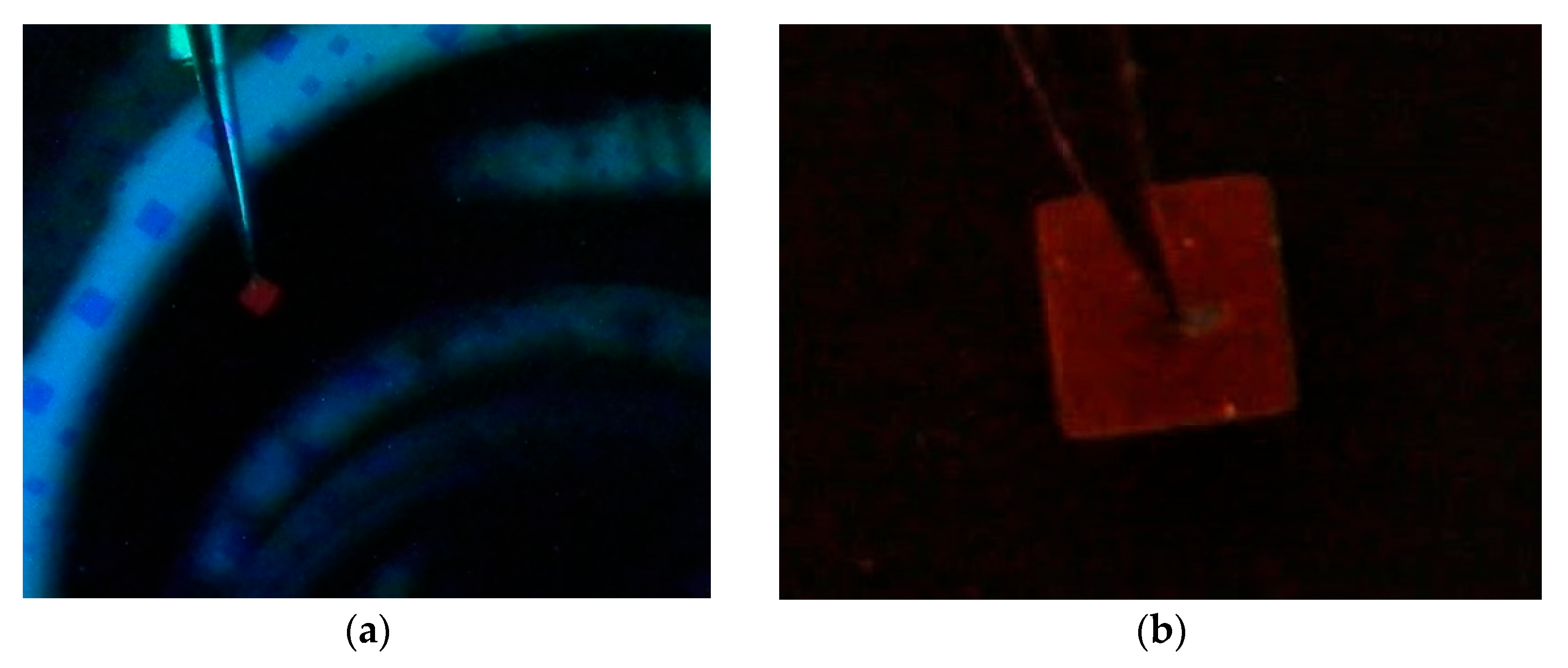
| Device | EL (nm)/Maximum Intensity (a.u.) | FWHM of EL (nm) | Voltage of EL (V) | J of EL (A/cm2) | B (eV) |
|---|---|---|---|---|---|
| PIN (FB) | 765/76.8 | 240 | 21 | 0.09 | 0.85 |
| PIN+N (FB) | 762/120.7 | 220 | 20 | 0.13 | 0.6 |
| PIN+N (RB) | 770/95 | 210 | −25 | 0.08 | 0.98 |
Publisher’s Note: MDPI stays neutral with regard to jurisdictional claims in published maps and institutional affiliations. |
© 2022 by the authors. Licensee MDPI, Basel, Switzerland. This article is an open access article distributed under the terms and conditions of the Creative Commons Attribution (CC BY) license (https://creativecommons.org/licenses/by/4.0/).
Share and Cite
Meneses-Meneses, M.; Moreno-Moreno, M.; Morales-Sánchez, A.; Ponce-Pedraza, A.; Flores-Méndez, J.; Mendoza-Cervantes, J.C.; Palacios-Huerta, L. Development of Heterojunction c-Si/a-Si1−xCx:H PIN Light-Emitting Diodes. Micromachines 2022, 13, 1948. https://doi.org/10.3390/mi13111948
Meneses-Meneses M, Moreno-Moreno M, Morales-Sánchez A, Ponce-Pedraza A, Flores-Méndez J, Mendoza-Cervantes JC, Palacios-Huerta L. Development of Heterojunction c-Si/a-Si1−xCx:H PIN Light-Emitting Diodes. Micromachines. 2022; 13(11):1948. https://doi.org/10.3390/mi13111948
Chicago/Turabian StyleMeneses-Meneses, Maricela, Mario Moreno-Moreno, Alfredo Morales-Sánchez, Arturo Ponce-Pedraza, Javier Flores-Méndez, Julio César Mendoza-Cervantes, and Liliana Palacios-Huerta. 2022. "Development of Heterojunction c-Si/a-Si1−xCx:H PIN Light-Emitting Diodes" Micromachines 13, no. 11: 1948. https://doi.org/10.3390/mi13111948