Article

Probabilistic Circuit Implementation Based on P-Bits Using the Intrinsic Random Property of RRAM and P-Bit Multiplexing Strategy

1
Zhejiang Lab, Hangzhou 311121, China
2
School of Microelectronics, Fudan University, Shanghai 200433, China
3
School of Microelectronics, University of Science and Technology of China, Hefei 230026, China
4
Key Laboratory of Microelectronic Devices Integrated Technology, Institute of Microelectronics of Chinese Academy of Sciences, Beijing 100029, China
*
Author to whom correspondence should be addressed.
Micromachines 2022, 13(6), 924; https://doi.org/10.3390/mi13060924
Submission received: 18 April 2022 / Revised: 5 June 2022 / Accepted: 8 June 2022 / Published: 10 June 2022
(This article belongs to the Section E:Engineering and Technology)

Abstract

:
Probabilistic computing is an emerging computational paradigm that uses probabilistic circuits to efficiently solve optimization problems such as invertible logic, where traditional digital computations are difficult to solve. This paper proposes a true random number generator (TRNG) based on resistive random-access memory (RRAM), which is combined with an activation function implemented by a piecewise linear function to form a standard p-bit cell, one of the most important parts of a p-circuit. A p-bit multiplexing strategy is also applied to reduce the number of p-bits and improve resource utilization. To verify the superiority of the proposed probabilistic circuit, we implement the invertible p-circuit on a field-programmable gate array (FPGA), including AND gates, full adders, multi-bit adders, and multipliers. The results of the FPGA implementation show that our approach can significantly save the consumption of hardware resources.

1. Introduction

In conventional computing systems, due to the constraints of the von Neumann architecture, huge computation and memory space and extremely long operation time are always required to solve many classical problems such as combinatorial optimization problems, neural networks, invertible logic, etc. To solve these problems effectively, new calculation methods have been continuously explored. Probabilistic computing, as a new computational paradigm, provides an attractive means to solve the above problem effectively with a small area and low power consumption, called a p-circuit [1,2]. The key role in the p-circuit is played by a probabilistic bit (p-bit), a robust unit fluctuating in time between 0 and 1, unlike conventional binary digital circuits where bits are used to represent a certain 0 or 1 [3], and a p-bit interacts with other p-bits in the same system using specific principles. Implementing the Boolean function with a p-circuit can achieve accuracy comparable to that of a standard digital circuit and, more importantly, is invertible, a unique feature not found in standard digital circuits. When operating in direct mode, the input is clamped, and the network provides the correct output. In the inverted mode, the output is clamped, and the network fluctuates between all possible inputs that are consistent with that output. When in floating mode, the network fluctuates between all the correct combinations of inputs and outputs.
Any random signal generator whose randomness can be tuned with a third terminal should be a suitable building block for the p-bit. In mathematical terms, p-bits can be described as Equation (1):
  m i ( t ) = s g n { r a n d ( 1 , 1 ) + t a n h ( I i ( t ) ) }
where r a n d   ( 1 , 1 ) represents a random number uniformly distributed between −1 and 1, t a n   h is an activation function, and s g n is the sign function (with binary 1 or −1 outputs). When the input I i ( t ) is zero, the output m i ( t ) takes on a value of −1 or 1 with equal probability. A large positive input makes the output more likely to be 1 while a large negative input makes the output more likely to be −1. Different p-bits can be interconnected according to
I i ( t ) = I 0 ( h i + j J i j m j ( t ) )
where J i j is the coupling coefficient, h i is the external bias, and I 0 controls the strength of the interconnections. The values of J i j , h i and I 0 are determined by the problem to be solved.
As mentioned above, one crucial part of constructing a p-circuit is implementing the p-bit in hardware. At present, there are three main ways to implement p-bits: Microcontrollers [3], digital circuits (field-programmable gate array (FPGA)/ASIC) [4,5], and new memory devices (MRAM, resistive random-access memory (RRAM)) [6,7,8]. There are two common problems in implementing p-bits with microcontrollers and digital circuits: One is the high energy consumption and the other is the waste of resources during operation. We can greatly reduce energy consumption by using new devices to implement p-bits, but as the number of p-bits increases, the variability between devices due to dispersion of the devices will need to be corrected [9]. We adopt the strategy of p-bit multiplexing, which reduces the waste of resources and avoids the additional design needed to correct the variability between devices, and finally achieves invertible logic with low power consumption and fewer resources.

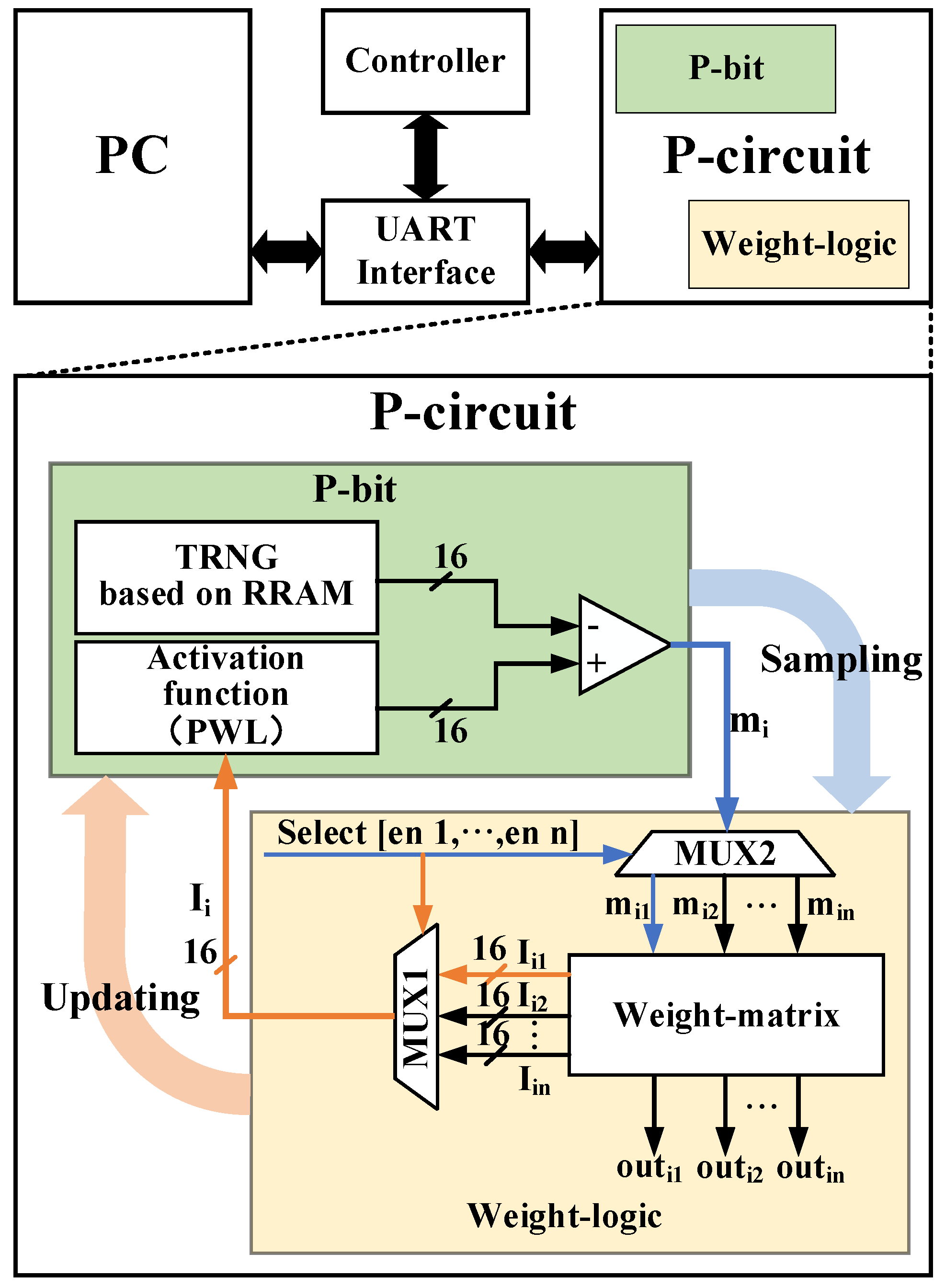
2. Proposed P-Bit Design

The overall structure diagram of the proposed probabilistic computing system is shown in Figure 1, which mainly includes the p-circuit, UART (Universal Asynchronous Receiver/Transmitter) interface, PC, and controller. The p-circuit completes the invertible logic, and the UART interface collects data and transmits it to the PC, the most important part of which is the components and implementation of the p-circuit. The p-circuit is the key to implementing invertible logic, which consists of a p-bit and weight-logic. In this section and the next section, we will describe and show the realization of the p-bit and weight logic in detail, respectively.
Since signals are represented by definite 0 and 1 in digital circuits, we convert Equation (1) into the following form:
  m i ( t ) = s t e p { r a n d ( 0 , 1 ) s i g m o i d ( I i ( t ) ) }
where r a n d ( 0 , 1 ) can be generated by the RRAM-based true random number generator (TRNG), the sigmoid function can be implemented by piecewise linear approximation (PWL), and the step function can be completed by the comparator. We will describe the specific implementation of these three parts separately below.

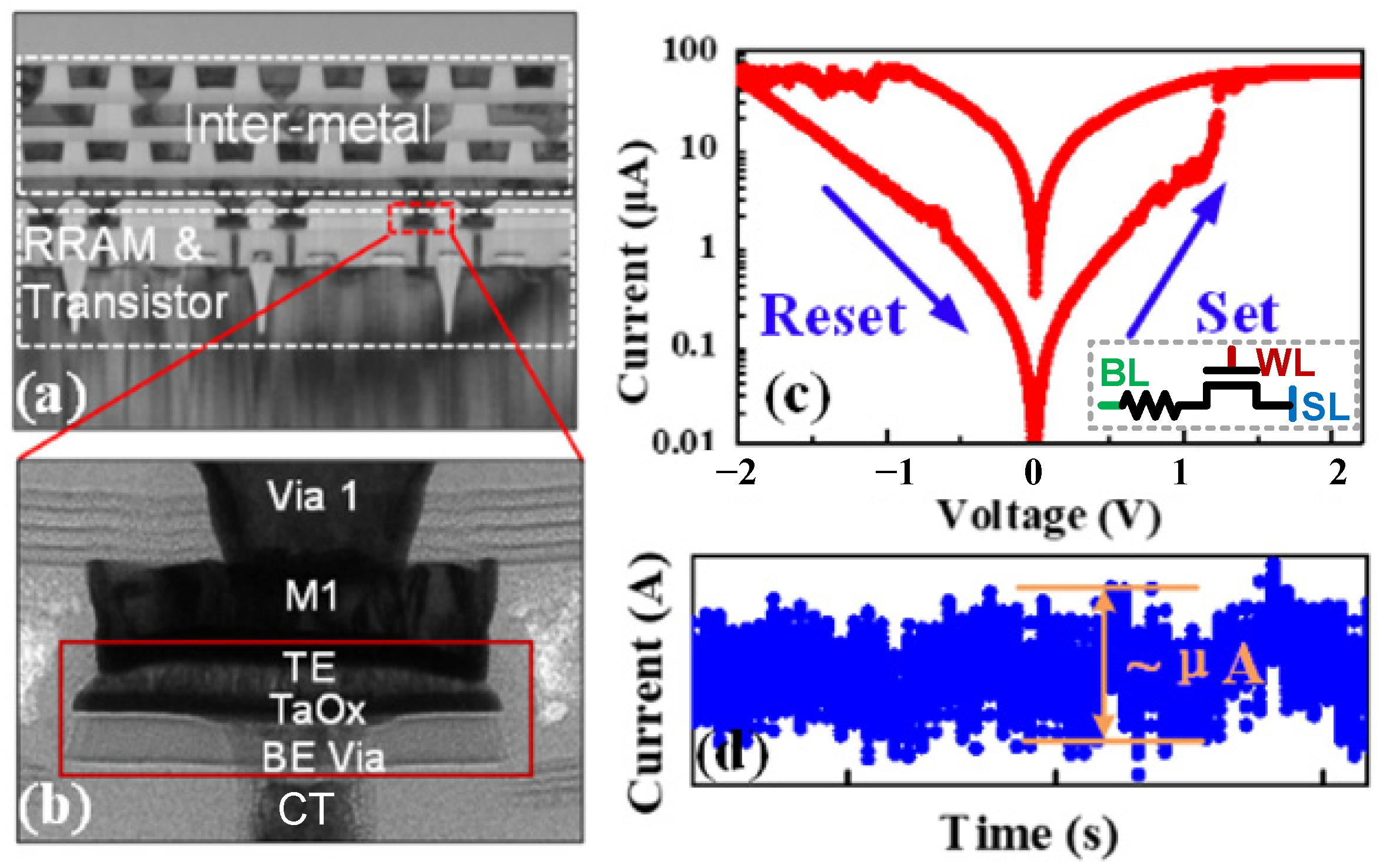
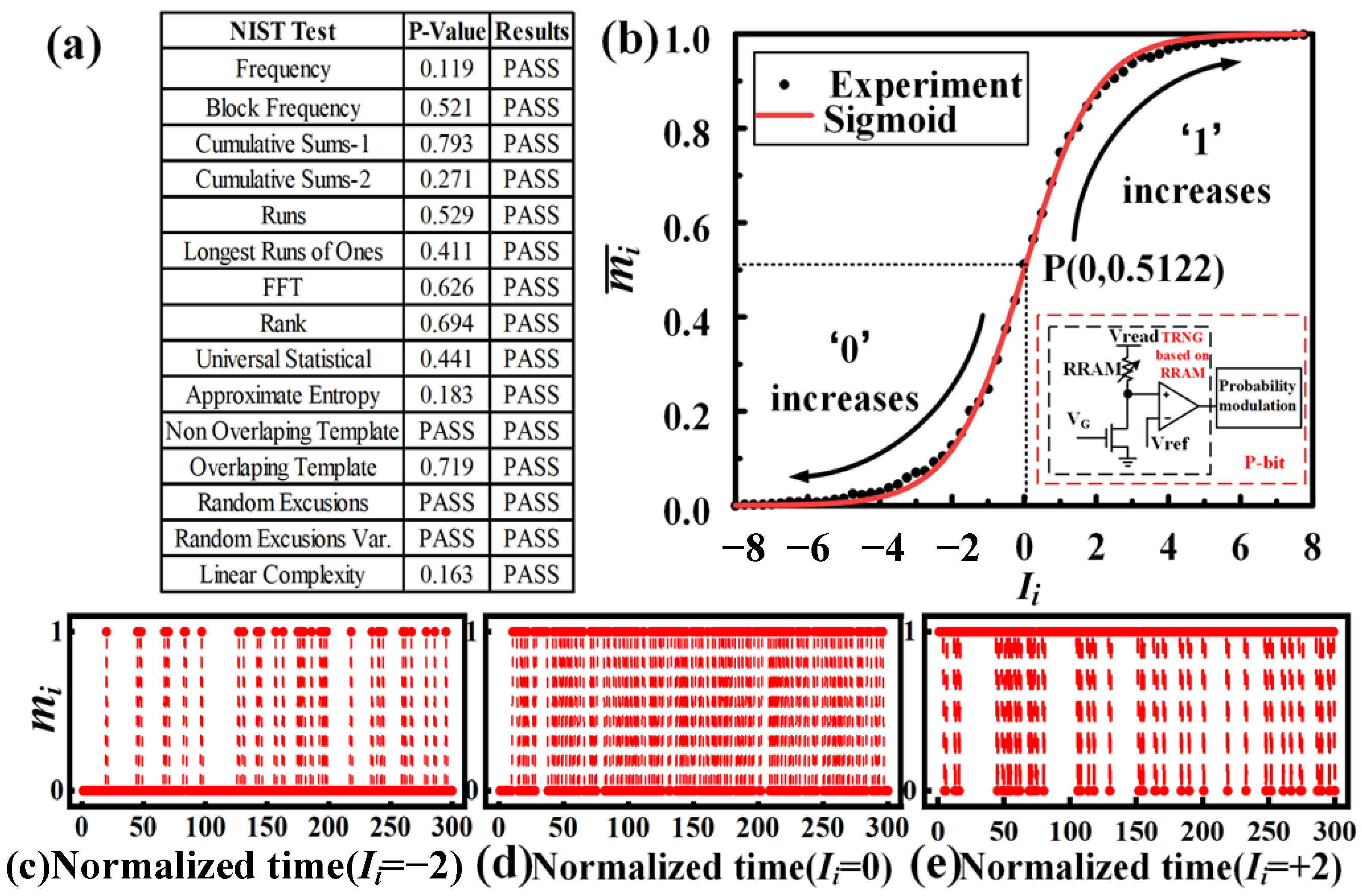
2.1. TRNG Based on RRAM

Compared with the traditional CMOS random number generator, the random number generator designed with RRAM has the advantages of a small area, low power consumption, and good randomness, which is more attractive [10,11,12,13]. The RRAM stack includes the bottom electrode (BE, TiN), top electrode (TE, TiN), and TaOx layer. The TaOx is deposited by PVD serving as the switching layer. Figure 2a shows the cross-section of RRAM cells in the array used in this study. The RRAM is built between contact (CT) and Metal 1 (M1). The magnified view of the RRAM cell structure is shown in Figure 2b. A TaOx switching layer was formed in the trench of M1 in connection with CT. An interface layer with a thickness of 1.5 nm∼5 nm was formed between the TaOx layer and TE. The detailed process flow of the RRAM device can be found in our previous work [14]. Figure 2c illustrates the typical DC I-V characteristics of the RRAM cell measured at room temperature, demonstrating a low 80 µA switching current and a low operation voltage below 1.5 V. During the DC test, the bias voltage of the transistor (NMOS) is 1.4 V due to the need for current limiting protection of the RRAM device during the set operation, while the SL is grounded, and the BL provides different DC voltages. For reset operation, the transistor bias voltage is 2.5 V, while BL is grounded, and SL provides different DC voltages.
The noise (including RTN [15] and flicker noise) affected by the local trap (a crystal defect or chemical center in a semiconductor capable of capturing electrons or holes) is shown in Figure 2d. The noise is utilized as the entropy source for the p-bit circuit in this work. The amplitude of the noise in the 28 nm RRAM can reach the order of microamps, making it easier to detect and utilize the noise to form a true random number generator compared to the noise of other new devices [16]. The noise extraction circuit is shown in the inset in Figure 3b. When the V G is high, the transistor is turned on, the corresponding RRAM unit is selected, and a small read voltage ( V r e a d   = 0.3 V) is applied to the RRAM. Due to the internal noise of the RRAM, the voltage at the positive input of the comparator is not fixed but has small voltage fluctuations. Upon comparing the V r e f with it, the comparator will output random 0 and 1 results. NIST 800-22 (National Institute of Standards and Technology, Gaithersburg, MD, USA) randomness test suites are performed on 10 M bits collected from the RRAM chip. As shown in Figure 3a, the data passed all test items, showing a high quality of randomness. The generated true random number will be used by the probability modulation module including the sigmoid function circuit and comparator to realize the bitstream with adjustable probability. Figure 3b shows the average value of m i obtained after 106 cycles of sampling when the input changes, which highly fits the sigmoid function. Figure 3c–e shows the statistical value of m i when I i is equal to −2, 0 and +2, respectively, over 300 cycles. When performing FPGA function implementation, we first sample and collect the random number sequence generated by the RRAM-based TRNG and store it in RAM, which continuously outputs the random number sequence to verify the function of the circuit.

2.2. Sigmoid Function

We use PWL [17] to implement the sigmoid function in the digital method, which is different from [4] using a lookup table (LUT) and [5] using a finite state machine (FSM). Since the input–output curve of the P-bit is highly coincident with the sigmoid function, and the sigmoid function tends to saturate when the input exceeds the interval [−8, +8], we restrict the input range of the sigmoid function to the interval [−8, +8] and use fifteen broken lines to approximate the sigmoid function. Then, the input and output of the sigmoid function are quantized by a 16-bit fixed-point number. For the input, we use one MSB to represent the sign, the middle three bits to represent the integer, and the rest to represent the decimal. For the output, all 16 bits are used to represent the decimal. Table 1 shows the truth table of the 15-segment polyline approximating the sigmoid function for x > 0 only, due to the symmetry of the sigmoid function. Taking the input range of 0 to 1 as an example, the slope of the broken line is 0.25, so the output starts at 0.5, and the decimal part of the input is shifted to the right by 2 places to achieve multiplication by 0.25. In this way, the use of multipliers can be avoided, effectively saving hardware resources.

2.3. Comparator

A 16-bit comparator compares the outputs of the sigmoid function and the TRNG. If the output of the activation function is larger than TRNG, the output m i is 1; otherwise, the output is 0. Figure 3b shows the time-average characteristics of p-bit, where m i ¯ is the statistical average value of m i over 106 sampling cycles. When the input I i is 0, m i randomly fluctuates between 0 and 1 with equal probability, so the time-average output m i is approximately equal to 0.5. As the input I i increases, the number of 1 generated by the p-bit will exceed the number of 0, increasing the time-averaged output m i ¯ .

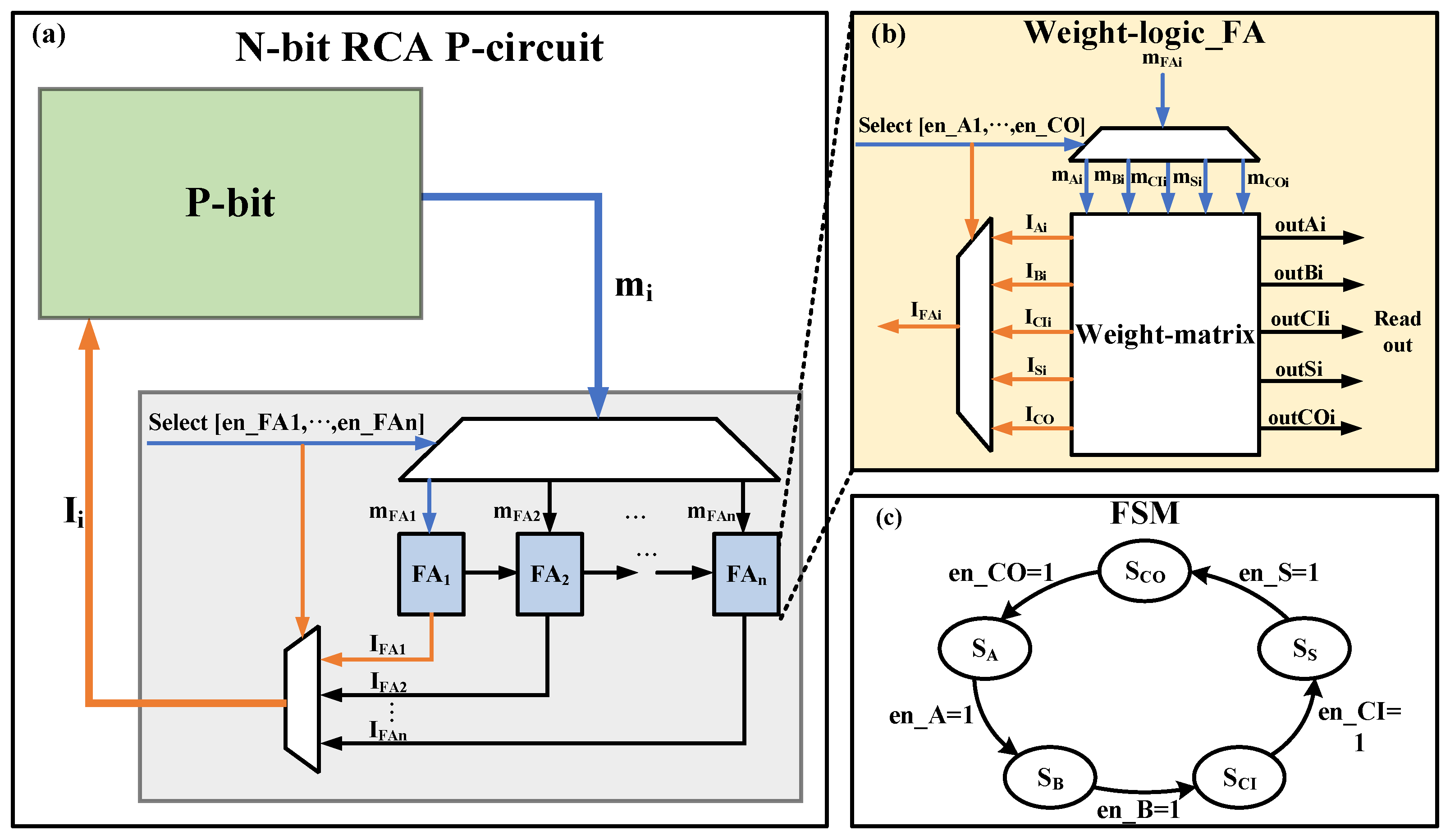
3. Weight-Logic Implementation
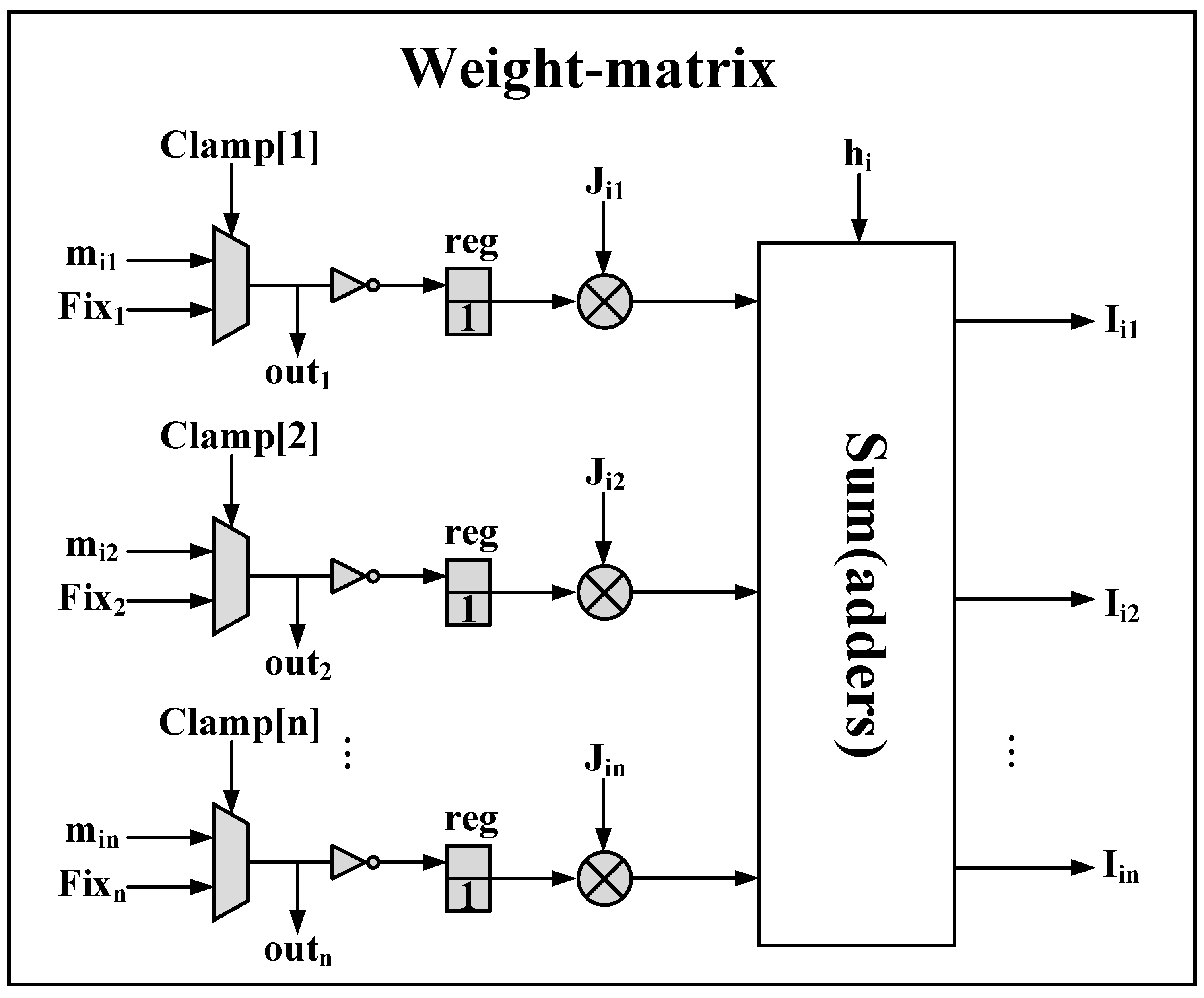
As mentioned above, the p-circuit consists of a p-bit and weight-logic. The p-bit is presented in Section 2, and adjusts the probability of output 1 according to the calculation result of the weight-logic and waits for the weight-logic to sample. In this section, we will show the design of the weight-logic, including the calculation of the weight-matrix and the multiplexing strategy applied therein.

3.1. Weight-Matrix

The weight-matrix implements Equation (2) employing adders and multipliers, the structure of which is shown in Figure 4. Sometimes it is necessary to fix the output of some p-bits to a certain value, so we use MUXs to choose between the fluctuation value ( m i n ) and the certain value ( F i x n ), which is controlled by the C l a m p [ 1 : n ] . Since m j in Equation (2) is bipolar ( m j { 1 , + 1 } ), the p-bit output m i in Equation (3) is unipolar ( m j { 0 , 1 } ), so we use 2-bit signed registers with LSB fixed to 1 for the conversion instead of linear mapping through y = 2 × m 1 , which can reduce one multiplication and one additional operation.

3.2. Multiplexing Strategy

For every p-circuit, there is a requirement that the p-bit must update serially. In [4], an additional sequencer circuit is used to force an updating sequence between p-bits. In this paper, we propose a multiplexing strategy to reduce the number of p-bits and complete the serial update of p-bits through FSM in the weight-matrix. Taking the N-bit ripple carry adder (RCA) as an example, in which we adopt the two multiplexing strategies. The first multiplexing strategy is applied to the basic unit full adder (FA) of RCA as shown in Figure 5b,c. Usually, it takes five p-bits to construct an FA, where A, B, and CI are the inputs of the FA, and S and CO are the outputs of the FA. In this work, we only need one p-bit as a generator to produce 0 or 1 probabilistically, while some registers store the states of the p-bit. This multiplexing strategy not only performs serial updates naturally but also greatly reduces the number of p-bits. We use two MUXs to achieve p-bit time-division multiplexing as shown in Figure 5b. The signal to control the MUX is generated by the weight-matrix module, and the concrete operation process is shown in Figure 5c. Starting with state 1, the circuit accomplishes two things in each state: Firstly, the input of the corresponding p-bit is calculated based on the interconnect coefficient ( J i j ), the external bias ( h i ), and the p-bit output ( m i ; secondly, the corresponding control signal is set to 1 to update the p-bit. An FA needs to go through five states to complete an update of all bits. The second multiplexing strategy is applied to N-bit RCA as shown in Figure 5a, and the update order is from FA1 to FAn. Although the multiplexing strategy increases the operation time, it is acceptable for statistical-based probabilistic computing to reduce hardware consumption.

4. Implementation Results

This section shows simulation results of the invertible AND gate, FA, 16-bit RCA, and 4-bit multiplier. The implementation of the invertible circuits in this section is based on the mathematical description of the p-bit and the coupling relationship between p-bits, as shown in Equations (1) and (2). In hardware, they correspond to the p-bit module and weight-logic module, respectively. The coupling weights J i j between p-bits are determined by the invertible logic problem to be implemented. The p-circuits system constantly updates its values and obtains the correct solution to the problem with a higher probability.

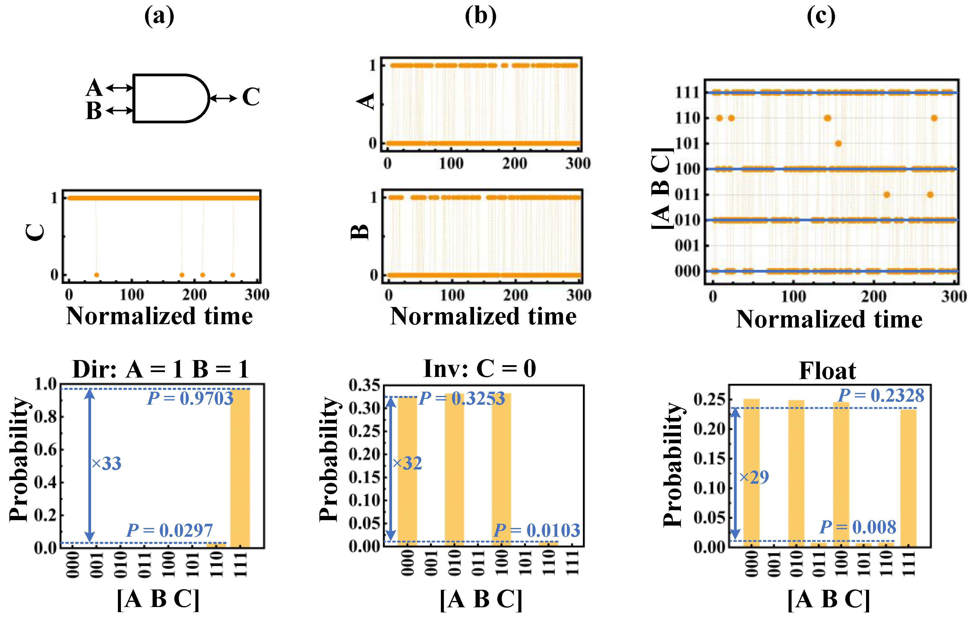
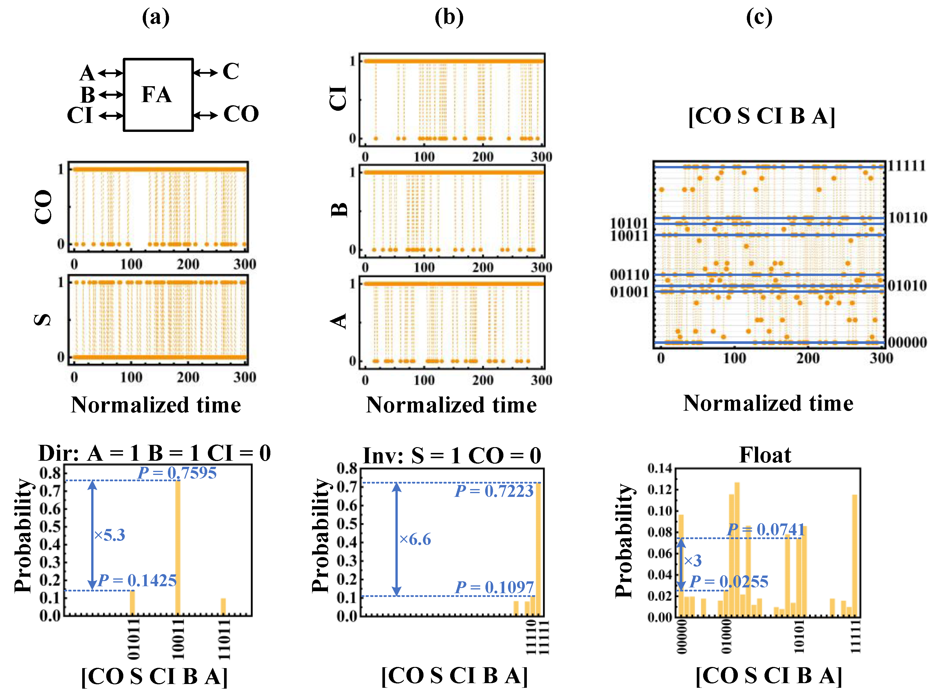
4.1. Invertible AND Gate and Full Adder (FA)

The invertible AND gate and FA can be implemented as p-circuits following the architecture of Figure 1 using the matrix J A N D , J F A and vector h A N D , h F A in Equations (4) and (5) [18].
  J A N D = [ 0 1 + 2 1 0 + 2 + 2 + 2 0 ]   h A N D = [ + 1 + 1 2 ]
J F A = [ 0 1 1 1 0 1 + 1 + 1 + 2 + 2 1 1 0 + 1 + 1 + 1 + 1 0 + 2 2 + 2 + 2 + 2 2 0 ]   h F A = [ 0 0 0 0 0 ]
For the invertible AND gate and FA, we have implemented three different modes: The directional mode, which clamps the inputs, the inverse mode, which clamps the output, and the floating mode where the input and output are floating. Figure 6 and Figure 7 show the steady-state statistics of the AND gate and FA. In Figure 6a, inputs A and B are clamped at 1 by Clamp and Fixn signals, and output C is held at 1 for a long time during 300 sampling cycles. Figure 6b shows the inverse mode where output C is clamped to 0. From the figure, the three combinations of input (A, B) have a relatively higher probability of occurrence, namely (0,0), (0,1), and (1,0), which is consistent with the truth table of the AND gate. In Figure 6c, all the inputs and output are floating, and the probabilities of all correct AND gate input and output combinations are significantly high, close to 0.25. Similar to the invertible AND gate, Figure 7 shows the results of the invertible FA. FA works in the directional mode when the input (A, B, CI) is clamped to (1,1,0), in the inverse mode when the output (S, CO) is clamped to (1,1), and in the floating mode when the input and output are floating. The invertible AND gate and FA require three clock cycles and five clock cycles, respectively, to complete a calculation.

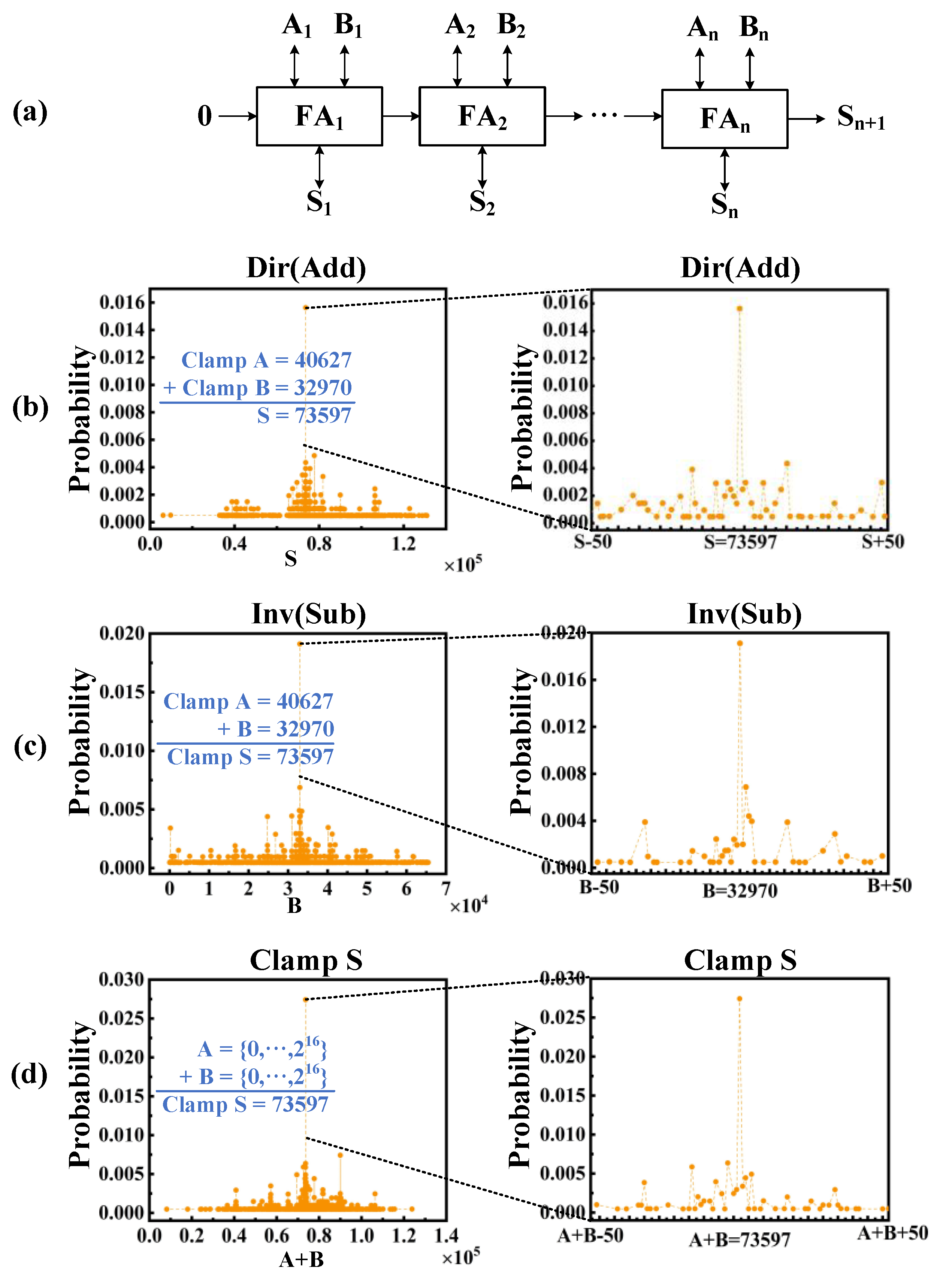
4.2. 16-Bit Ripple Carry Adders (RCA)

We cascade the constructed invertible FAs to form an N-bit RCA as shown in Figure 8a, and randomly select the data A = 40,627, B = 32,970 as an example to illustrate the three different modes of the invertible 16-bit RCA. In Figure 8b, RCA works in the directional mode (used for addition), A and B are clamped through Clamp and Fixn signals, and S is countered for a long time. The probability of the correct result is significantly high (near 0.016) among the 217 possibilities. In Figure 8c, we clamp A and S to use RCA as a subtraction in inverse mode, and the probability of B = 32,970 is much higher than the others, which are close to 0.019. In Figure 8d, we clamp only S and calculate the sum of A and B. The highest probability (close to 0.028) is for A + B = 73,597. Figure 8d shows a great ability to extract the correct answer despite large fluctuations, which is useful in some NP problems such as the Subset Sum Problem. The invertible 16-bit RCA requires 80 clock cycles to complete a calculation.

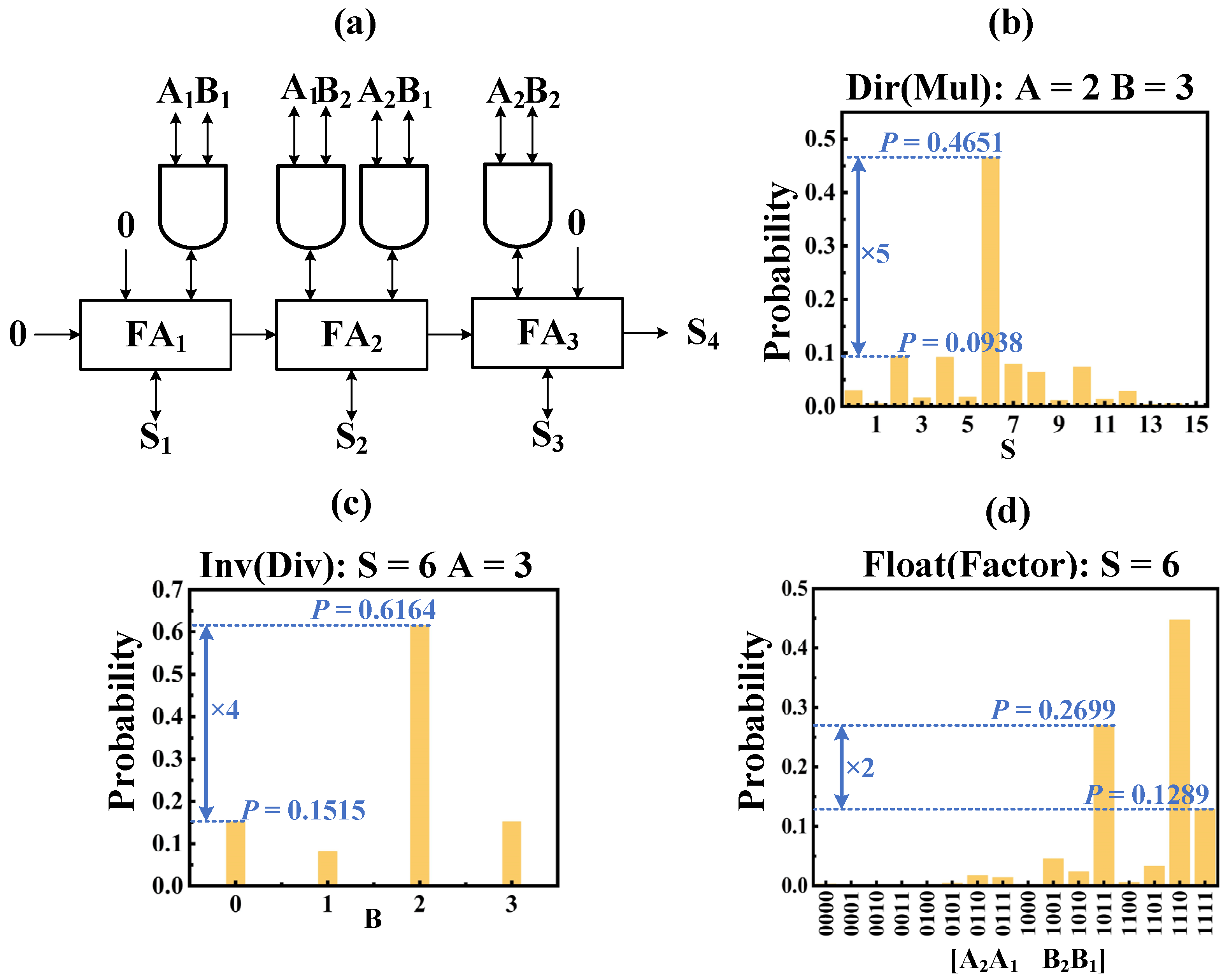
4.3. 4-Bit Multiplier

We construct a 4-bit multiplier consisting of four invertible AND gates and three invertible FAs as shown in Figure 9, which can be applied to multiplication, division, and factorization. We take 2 × 3 = 6 as an example to illustrate these three functions of the multiplier. In the multiplication process, we clamp A = 2, B = 3, and count S ([S4, S3, S2, S1]), and S = 6 appears with the highest probability, close to 0.45. In this division, we clamp A = 2, S = 6, and count B ([B2, B1]), with B = 2 taking place with the highest probability, close to 0.6. In factorization, we just clamp S = 6 and count A and B ([A2, A1, B2, B1]), and the relatively high probability of (1101) and (1011) implies that A = 2, B = 3 or A = 3, B = 2 is more likely. An invertible 4-bit multiplier requires 18 clock cycles to complete a calculation.

5. Conclusions

In this work, invertible logic circuits are realized by combining RRAM and digital circuits. Table 2 shows a comparison between the previous work and this work in terms of a hardware implementation of invertible logic. We design an RRAM-based TRNG to replace the pseudo-random number generator formed by the linear feedback shift register (LFSR) and combined it with the activation function implemented by PWL to form a standard p-bit unit. We also propose a p-bits multiplexing strategy to save hardware resources. Since our work is primarily based on a digital circuit approach, we also compare this work with two previous works on purely digital circuit implementations in terms of hardware resources such as the number of LUTs and registers required, as shown in Table 3. Table 3 shows the number of LUTs and registers used in this work, [4], and [5] to implement invertible AND gates, invertible FA, and invertible 32-bit RCA, respectively. The percentage based on [5] can more intuitively illustrate the superiority of this work in saving resource utilization. We use the Xilinx Kintex ultrascale XCKU0401-FBVA676 FPGA (San Jose, CA, USA). From the circuit structure analysis, the RRAM-based TRNG uses more than 100 times fewer transistors than the LFSR [9], and our method has greatly reduced hardware resources.

Author Contributions

Data curation, Y.L., X.L. and B.P.; visualization, Y.L.; writing—original draft preparation, Y.L.; software, Q.H.; writing—review & editing, Q.H.; Q.W. and J.Y.; methodology, Q.W. and Y.Z.; formal analysis, D.Z. and Q.D., investigation, Z.H. and Y.H.; validation, J.C. and H.J.; funding acquisition, J.Y.; supervision, X.X., H.L. and J.Y. All authors have read and agreed to the published version of the manuscript.

Funding

This work was supported in part by the National Key R&D Program of China under Grant No. 2018YFB2202900, in part by the Major Scientific Research Project of Zhejiang Lab (No.2022PF0AC01), and in part by the National Natural Science Foundation of China under Grants 92164204, 61904200, and 62025406 and the Strategic Priority Research Program of the Chinese Academy of Sciences under Grant No. XDB44000000.

Data Availability Statement

The data that support the findings of this study are available from the corresponding author upon request.

Conflicts of Interest

The authors declare no conflict of interest.

References

  1. Sutton, B.; Camsari, K.Y.; Behin-Aein, B.; Datta, S. Intrinsic optimization using stochastic nanomagnets. Sci. Rep. 2017, 7, 44370. [Google Scholar] [CrossRef] [PubMed] [Green Version]
  2. Lin, Y.; Zhang, Q.; Tang, J.; Gao, B.; Li, C.; Yao, P.; Liu, Z.; Zhu, J.; Lu, J.; Hu, X.S.; et al. Bayesian Neural Network Realization by Exploiting Inherent Stochastic Characteristics of Analog RRAM. In Proceedings of the 2019 IEEE International Electron Devices Meeting (IEDM), San Francisco, CA, USA, 7–11 December 2019. [Google Scholar]
  3. Pervaiz, A.Z.; Ghantasala, L.A.; Camsari, K.Y.; Datta, S. Hardware emulation of stochastic p-bits for invertible logic. Sci. Rep. 2017, 7, 10994. [Google Scholar] [CrossRef] [PubMed] [Green Version]
  4. Pervaiz, A.Z.; Sutton, B.M.; Ghantasala, L.A.; Camsari, K.Y. Weighted p-Bits for FPGA Implementation of Probabilistic Circuits. IEEE Trans. Neural Netw. Learn. Syst. 2018, 30, 1920–1926. [Google Scholar] [CrossRef] [PubMed] [Green Version]
  5. Smithson, S.C.; Onizawa, N.; Meyer, B.H.; Gross, W.J.; Hanyu, T. Efficient CMOS invertible logic using stochastic computing. IEEE Trans. Circuits Syst. I Regul. Pap. 2019, 66, 2263–2274. [Google Scholar] [CrossRef]
  6. Camsari, K.Y.; Salahuddin, S.; Datta, S. Implementing p-bits with embedded MTJ. IEEE Electron Device Lett. 2017, 38, 1767–1770. [Google Scholar] [CrossRef]
  7. Camsari, K.Y.; Faria, R.; Sutton, B.M.; Datta, S. Stochastic p-bits for invertible logic. Phys. Rev. 2017, 7, 031014. [Google Scholar] [CrossRef] [Green Version]
  8. Faria, R.; Camsari, K.Y.; Datta, S. Low-barrier nanomagnets as p-bits for spin logic. IEEE Magn. Lett. 2017, 8, 1–5. [Google Scholar] [CrossRef]
  9. Borders, W.A.; Pervaiz, A.Z.; Fukami, S.; Camsari, K.Y.; Ohno, H.; Datta, S. Integer factorization using stochastic magnetic tunnel junctions. Nature 2019, 573, 390–393. [Google Scholar] [CrossRef] [PubMed]
  10. Jiang, H.; Belkin, D.; Savel’ev, S.E.; Lin, S.; Wang, Z.; Li, Y.; Joshi, S.; Midya, R.; Li, C.; Rao, M.; et al. A novel true random number generator based on a stochastic diffusive memristor. Nat. Commun. 2017, 8, 882. [Google Scholar] [CrossRef] [PubMed] [Green Version]
  11. Rai, V.K.; Tripathy, S.; Mathew, J. Memristor based random number generator: Architectures and evaluation. Procedia Comput. Sci. 2018, 125, 576–583. [Google Scholar] [CrossRef]
  12. Stoller, S.; Campbell, K.A. Demonstration of three true random number generator circuits using memristor created entropy and commercial off-the-shelf components. Entropy 2021, 23, 371. [Google Scholar] [CrossRef] [PubMed]
  13. Taskiran, Z.G.C.; Taşkıran, M.; Kıllıoğlu, M.; Kahraman, N.; Sedef, H. A novel memristive true random number generator design. COMPEL Int. J. Comput. Math. Electr. Electron. Eng. 2019, 38, 208–224. [Google Scholar] [CrossRef]
  14. Lv, H.; Xu, X.; Yuan, P.; Dong, D.; Gong, T.; Liu, J.; Yu, Z.; Huang, P.; Zhang, K.; Huo, C.; et al. BEOL based RRAM with one extra-mask for low cost, highly reliable embedded application in 28 nm node and beyond. In Proceedings of the 2017 IEEE International Electron Devices Meeting (IEDM), Piscataway, NJ, USA, 2–6 December 2017. [Google Scholar]
  15. Veksler, D.; Bersuker, G.; Vandelli, L.; Padovani, A.; Larcher, L.; Muraviev, A.; Chakrabarti, B.; Vogel, E.; Gilmer, D.C.; Kirsch, P.D. Random telegraph noise (RTN) in scaled RRAM devices. In Proceedings of the 2013 IEEE International Reliability Physics Symposium (IRPS), Monterey, CA, USA, 14–18 April 2013. [Google Scholar]
  16. Gong, T.; Dong, D.; Luo, Q.; Xu, X.; Yang, J.; Yu, J.; Ding, Q.; Lv, H.; Liu, M. Quantitative Analysis on Resistance Fluctuation of Resistive Random Access Memory by Low Frequency Noise Measurement. IEEE Electron Device Lett. 2021, 42, 312–314. [Google Scholar] [CrossRef]
  17. Tommiska, M.T. Efficient digital implementation of the sigmoid function for reprogrammable logic. IEE Proc. Comput. Digit. Tech. 2003, 150, 403–411. [Google Scholar] [CrossRef] [Green Version]
  18. Biamonte, J.D. Nonperturbative k-body to two-body commuting conversion Hamiltonians and embedding problem instances into Ising spins. Phys. Rev. A 2008, 77, 052331. [Google Scholar] [CrossRef] [Green Version]
Figure 1. Block diagram of a probabilistic computing system including p-circuit, UART interface, PC, and controller (top). Detailed p-circuit structure (bottom): P-bit (green), weight-logic (yellow).
Micromachines 13 00924 g001
Figure 2. Structure and characteristics of RRAM. (a) The cross-section of RRAM cell in a 28 nm process 1T1R array. The RRAM unit is built between contact and Metal 1; (b) the magnified view of the cell structure; (c) typical DC I-V characteristics of the RRAM cell and structure of 1T1R RRAM; (d) the noise measured in the 28 nm RRAM cell; the array size is 16 Kb.
Micromachines 13 00924 g002
Figure 3. Probabilistic-adjustable randomness of P-bit. (a) NIST-verified results at p = 0.5; (b) the time-averaged output of p-bit, which fits sigmoid well; (ce) the statistical value of m i when I i is equal to −2, 0, +2, respectively, over 300 cycles.
Micromachines 13 00924 g003
Figure 4. The structure of the weight-matrix. MUXs are used to choose the fluctuation value ( m i n ) or a certain value ( F i x n ). 2-bit signed registers with LSB fixed to 1 are used to convert p-bit output m { 0 , 1 } to a bipolar m { 1 , + 1 } representation.
Micromachines 13 00924 g004
Figure 5. Proposed N-bit ripple carry adder (RCA). (a) The structure of N-bit RCA p-circuit using two-multiplexing strategy; (b) the structure of FA using time-division multiplexing; (c) the calculation process in the weight-matrix.
Micromachines 13 00924 g005
Figure 6. Invertible AND gate operation. (a) Directional mode: Clamping the inputs (A, B) to (1,1), the time-dependent output of C for the AND gate (top), the statistics collected for 106 samples (bottom); (b) inverse mode: Clamping the outputs C to 0, time-dependent outputs of (A, B) for the AND gate (top), the statistics collected for 106 samples (bottom); (c) floating mode: All the inputs and output are floating, time-dependent nodes of (A, B, C) for the AND gate (top), the statistics collected for 106 samples (bottom).
Micromachines 13 00924 g006
Figure 7. Invertible full adder operation, similar to invertible AND gate including directional mode (a), inverse mode (b), and floating mode (c).
Micromachines 13 00924 g007
Figure 8. Invertible 16-bit RAC operation. (a) N-bit RCA is designed based on constructed invertible full adders; (b) clamping A and B working in directional mode (used for addition). The left is the statistics of S over a period, and the right is the statistics of 100 samples around the correct S; (c) clamping A and S working in inverse mode (used for subtraction); (d) only clamping S, and the statistics of A + B.
Micromachines 13 00924 g008
Figure 9. Invertible 4-bit multiplier operation. (a) The structure of 4-bit multiplier based on invertible AND gates and FA; (b) multiplication: Clamping A = 2, B = 3, the statistics of S; (c) division: Clamping A = 2, S = 6, the statistics of B; (d) factorization: Clamping S = 6, the statistics of A and B.
Micromachines 13 00924 g009
Table 1. The truth table of the 15-segment polyline approximates the sigmoid function for x > 0.
Input RangeInput ValueOutput RangeOutput ValueSlope
[0, 1)0000xxxxxxxxxxxx[0.5, 0.75)10xxxxxxxxxxxxxx0.25
[1, 2)0001xxxxxxxxxxxx[0.75, 0.875)110xxxxxxxxxxxxx0.125
[2, 3)0010xxxxxxxxxxxx[0.875, 0.9375)1110xxxxxxxxxxxx0.0625
[3, 4)0011xxxxxxxxxxxx[0.9375, 0.96875)11110xxxxxxxxxxx0.03125
[4, 5)0100xxxxxxxxxxxx[0.96875, 0.984375)111110xxxxxxxxxx0.015625
[5, 6)0101xxxxxxxxxxxx[0.984375, 0.9921875)1111110xxxxxxxxx0.0078125
[6, 7)0110xxxxxxxxxxxx[0.9921875, 0.99609375)11111110xxxxxxxx0.00390625
[7, 8)0111xxxxxxxxxxxx[0.99609375, 1)11111111xxxxxxxx0.001953125
Table 2. Hardware implements of invertible logic.
Ref.P-BitOutput Value
RNGActivation Function
[3]MCUMCU (sigmoid)MCU
[4]LFSRLUT (tanh)FPGA
[5]LFSRFSM (tanh)ASIC and FPGA
[6]MTJNo needResistance network
This workRRAMPWL (sigmoid)FPGA
Table 3. FPGA resource utilization of the invertible logic circuit.
Invertible Logic CircuitThis Work[5][4]This Work/[5]
LUTsRegistersLUTsRegistersLUTsRegistersLUTsRegisters
AND455925730715612317.5%19.2%
FA8576400329134558621.3%23.1%
32-bit RCA2731167810,455191038,81418,07126.1%87.9%
Publisher’s Note: MDPI stays neutral with regard to jurisdictional claims in published maps and institutional affiliations.

