Article

Pre–Placed Metal Laser–Additive Manufacturing on Grade 5 Titanium Substrate: Layer Formation, Oxidation Resistance, and Wear Resistance

1
School of Materials Science and Engineering, Shanghai University of Engineering Science, Shanghai 201620, China
2
School of Materials Science and Engineering, Shanghai Jiao Tong University, Shanghai 200240, China
3
Shanghai Collaborative Innovation Center of Laser Advanced Manufacturing Technology, Shanghai University of Engineering Science, Shanghai 201620, China
4
Department of Chemical and Materials Engineering, University of Alberta, Edmonton, AB T6G 1H9, Canada
*
Authors to whom correspondence should be addressed.
Metals 2023, 13(8), 1372; https://doi.org/10.3390/met13081372
Submission received: 16 June 2023 / Revised: 8 July 2023 / Accepted: 28 July 2023 / Published: 30 July 2023

Abstract

:
The laser parameters and additive materials were investigated for the laser–additive manufacturing of titanium alloys. A pre–placed metal–strip–based method for 3D printing titanium components was proposed. Before laser processing, the metal strips were fixed to a Grade 5 titanium substrate using resistance spot welding. The effect of the processing conditions (laser power: 1.5–3.0 kW; scanning speed: 3–9 mm·s−1; one or three layers; 1, 6, or 12 passes; Grade 2 and Grade 5 as additives) on the microstructures, oxidation resistance, and wear resistance of the as–printed samples was investigated. The results showed that the microstructure consisted of α′ martensite, oxygen–stabilized α, transformed β that contains coarse and fine acicular α, titanium oxides, and carbides. Cracks were observed, particularly near the upper surface of the three–layer samples. The cracks were suggested to have formed due to cumulative residual stresses and the formation of oxygen–stabilized α and α′ martensite that might cause embrittlement. Both oxidation and wear tests were conducted to verify the improved performance. After 55 h of oxidation, the as–printed samples showed mass gains of 0.029–0.035 g·cm−2, which were smaller than those of the substrate (0.039 g·cm−2).

1. Introduction

In materials processing, the performance of a product is influenced by the chemical composition of the material [1,2,3,4,5,6,7,8], the processing method [9,10], the equipment, and the parameters [11]. Materials such as iron, copper, aluminum, and titanium have a wide range of applications in manufacturing, construction, electronics, and other industries. The high specific strength and stiffness of titanium alloys mean they were extensively used in aircraft, spacecraft, and rockets as well as in biomedical implants where a light weight, a high strength, toughness, temperature resistance, and biocompatibility are important properties [1,12].
Hartbower et al. [12] evaluated the feasibility of as–welded titanium alloys for missile applications. In addition, the use of titanium alloys as thermal protection in hypersonic aircraft and the ignition of titanium alloys in aerodynamic heating were investigated [13]. Tobe et al. [14] proposed a novel deployable rocket nozzle utilizing the superelasticity of titanium. Prestat et al. [15] summarized the applications of titanium alloys in the fields of orthopedics and dentistry. However, Bai et al. [16] suggested that the “inverse relationship” between hardness and toughness has limited the application of titanium. A potential solution to this problem is additive manufacturing.
The methods used for additive manufacturing—including laser, arc, or electron beam deposition or hybrids thereof—were summarized by Kruth et al. [17]. A significant effort has been made to address the challenges related to dimensional accuracy and to make additive manufacturing a production technique. Beese et al. [18] reviewed the additive manufacturing of titanium parts by directed energy deposition and powder–bed fusion. Denlinger et al. [19] suggested that an accumulation of distortion occurred during the build process, and the distortion and residual stress levels decreased with the increasing dwell time. Ghouse et al. [20] optimized the laser parameters and scanning strategies and increased the fatigue strength. Wang et al. [21] proposed the laser metal deposition (LMD) method based on the wire–based additive manufacturing process.
Murr et al. [22] reported that a relatively high dislocation density contributed to the residual hardness. Juechter et al. [23] proposed a selective electron beam manufacturing (EBM) process for fabricating complex titanium components. Karlsson et al. [24] suggested that the final oxide was formed in the chamber after melting. Bambach et al. [25] exploited the advantages of additive manufacturing and forging operations by combining both processes. Soro et al. [26] investigated the surface modification of titanium lattice structures using selective laser melting (SLM) and a chemical post–treatment. Thijs et al. [27] further investigated SLM and reported specific conditions, short interactions, high temperature gradients, and high localization. Hollander et al. [28] used a direct laser–forming method to produce metal on the titanium substrate for application as a hard tissue biomaterial.
The additive (or filler) material was found to be another important factor affecting the mechanical properties. Verma et al. [29] used an in situ modification method to improve the wear resistance of titanium parts with incremental additions of boron. Lu et al. [30] improved the wettability of nickel with copper, the microstructure, and the surface quality of laser–fabricated parts due to welding metallurgy and improved the wettability of copper with titanium carbide. Guo et al. [31] found that the Al–rich layer prevented oxygen diffusion and improved oxidation resistance. Fox et al. [32] fabricated tantalum coatings on titanium substrate to improve the interface compatibility. Dutta et al. [33] found that additive manufacturing offered economic advantages over the conventionally processed material. Trevisan et al. (Ref. [34]) discussed the wire–feed strategy based on the SLM, EBM, and LMD methods. Tapoglou et al. [35] successfully controlled the oxygen content in microstructures using bath and bag shielding strategies. Kelly et al. [36] established the relationships between post–processing, microstructure, and fatigue strength.
The directed energy deposition (DED) process with a strip–shaped material has the advantages of flexibility, a low cost, and a high utilization rate. Moghimian et al. [37] evaluated the reusability and recycling of titanium alloy powder in DED. Amado et al. [38] investigated the use of pure titanium sponge powders as an alternative in DED.
The present work aims to verify the feasibility of the proposed metal–strip–based laser–additive DED process and provide a method that allows researchers and engineers to design additive materials, which may expand the diversity of the available strip additive materials. The additive layers were prepared on the surface of a Grade 5 (Gr5) titanium substrate using an additive manufacturing method with pre–placed commercially pure Grade 2 (Gr2) titanium and Grade 5 (Gr5) titanium wires. The investigation focused on the effects of laser parameters and additive materials on the microstructure, oxidation resistance, and wear resistance.
This paper reports the wire–fed additive manufacturing process, especially on the wire feeding setup, which is indispensable to wire–fed additive manufacturing. The innovation of this paper lies in the use of two types of wires, TA2 and TC4, as additive materials and proposes a laser wire–fed additive manufacturing method based on pre–placed wire strips. The layer formation, high–temperature oxidation resistance, and wear resistance of the samples produced by this method under different process parameters are investigated.

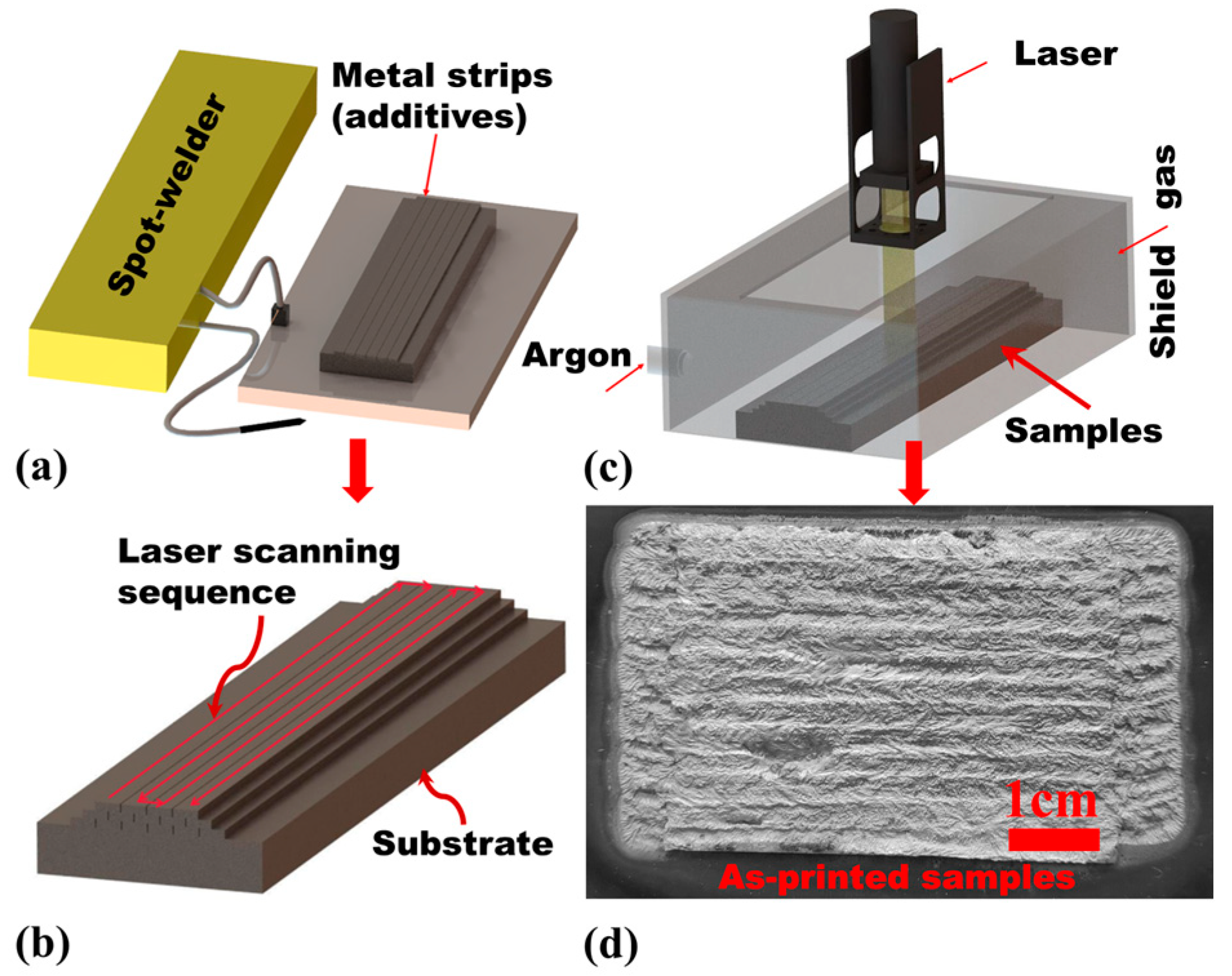
2. Materials and Methods

The chemical composition (wt %) of the 6 mm thick Grade 5 titanium substrate (100 mm × 100 mm) is shown in Table 1. The additive materials were strips of commercially pure Grade 2 and Grade 5 titanium. These metal strips were prepared using DK7730 wire electrical–discharge machining (Haishu, Ningbo, China). The substrates and metal strips were polished with silicon carbide abrasive paper to remove the oxide layer. The metal strips were resistance–spot–welded on the substrate before additive manufacturing. The manufacturing details were as follows (see Figure 1a,b):
  • The Grade 5 alloy substrate was placed on a conductive metal plate.
  • One pole of a Hotspot II Heavy Duty Welder (DCC, DCC Corporation, Camden County, NJ, USA) was connected to the conductive metal plate. The strip–shaped additive materials were pre–placed side by side on the substrate and clamped.
  • Resistance spot welding of the additive layer was conducted using the other pole of the spot welder. The distance between two adjacent welding spots was 300 mm, and the energy was 180 J per pulse.
  • Different passes, layers, and laser parameters—as shown in Table 2—were chosen as the main variables to assess how these factors affect the structure and properties of the resulting specimens.
The equipment used for laser–additive manufacturing (Figure 1b) was a 5 kW maximum output YLS–5000 (IPG, Oxford, MA, USA) fiber laser with an ABB–IRB 4600 (ABB, Zürich, Switzerland) robot and BIMO QBH (HIGHYAG, Kleinmachnow, Germany) laser processing head. Argon was used as the shielding gas at 25 L·min−1 flow rate to protect the specimen from oxidation. The dimension of laser facular was 5 mm × 5 mm, and the laser scanning strategy (Figure 1c) was reciprocating scanning. The laser parameters are shown in Table 2, and the as–printed samples are shown in Figure 1d. The selection of laser parameters was mainly based on the experiments. Samples P1–P6 were used for laser parameter selection, and samples T1–T9 were used for further investigation.
The metallographic specimens were etched with Kroll’s reagent (HF:HNO3:H2O = 2:5:93) for 15 s. The microstructure was studied using TESCAN VEGA3 (TESCAN, Kohoutovice, Czech Republic) and S–3400N (Hitachi, Tokyo, Japan) scanning electron microscopes. Surface and internal defects of the as–printed layers were non–destructively evaluated by X-ray radiography. During the radiographic examination, 12 tests were performed in accordance with GB/T3323–2005A III, using an XXG–2005 X-ray source (EBP, Shanghai, China) at 110 kV.
X-ray diffraction measurements of oxidation layers were conducted on an X’Pert PRO X-ray diffractometer (PANalytical, Almelo, The Netherlands) with Cu–Kα radiation (λ = 0.15406 nm). Scans were performed from 10° to 90° with a step size of 0.02°.
The wear resistance of the specimens was measured with steel as the friction pair using a HT–1000 high–temperature tribometer (CETR, Campbell, CA, USA) under dry wear conditions. The test parameters were sliding time, 30 min; friction pairs, 6 mm diameter GCr15 steel balls; radius of rotation, 2 mm; sliding velocity, 280 rpm·min−1; and load, 1120 g. From the values stored in the databank, coefficient of friction (COF) vs. time plots and mean COF values were obtained.
The high–temperature oxidation resistance of the specimens was evaluated using SXL–1700C box electric furnaces (SIOMM, Shanghai, China) maintained at 800 °C for 55 h with sample dimensions of 10 mm × 10 mm × 1 mm. Sample oxidation was measured every hour for the first 10 h, then every 2 h over the next 20 h, and finally every 5 h during the remaining hold time.

3. Results

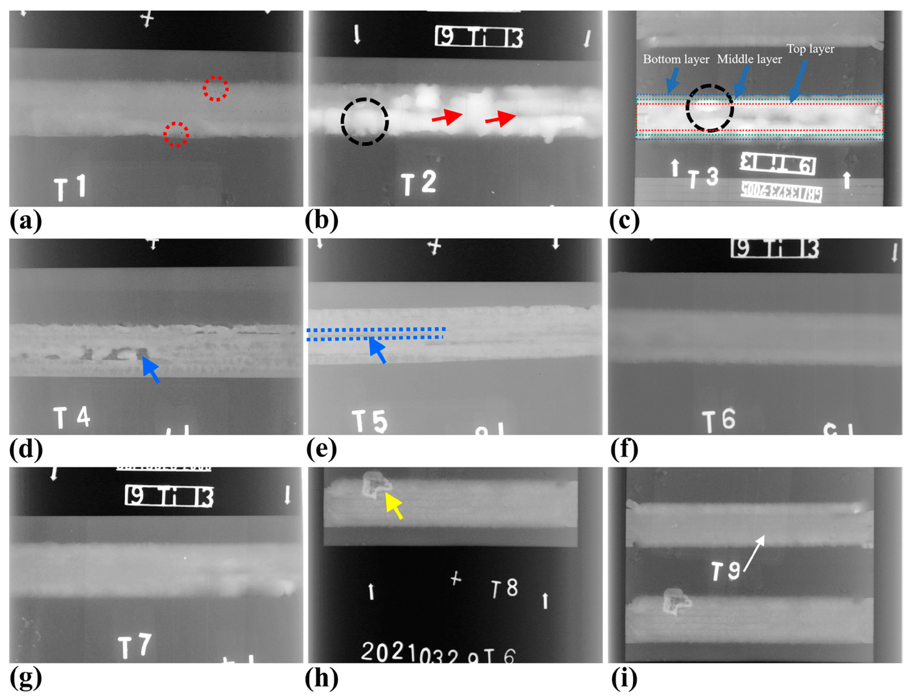
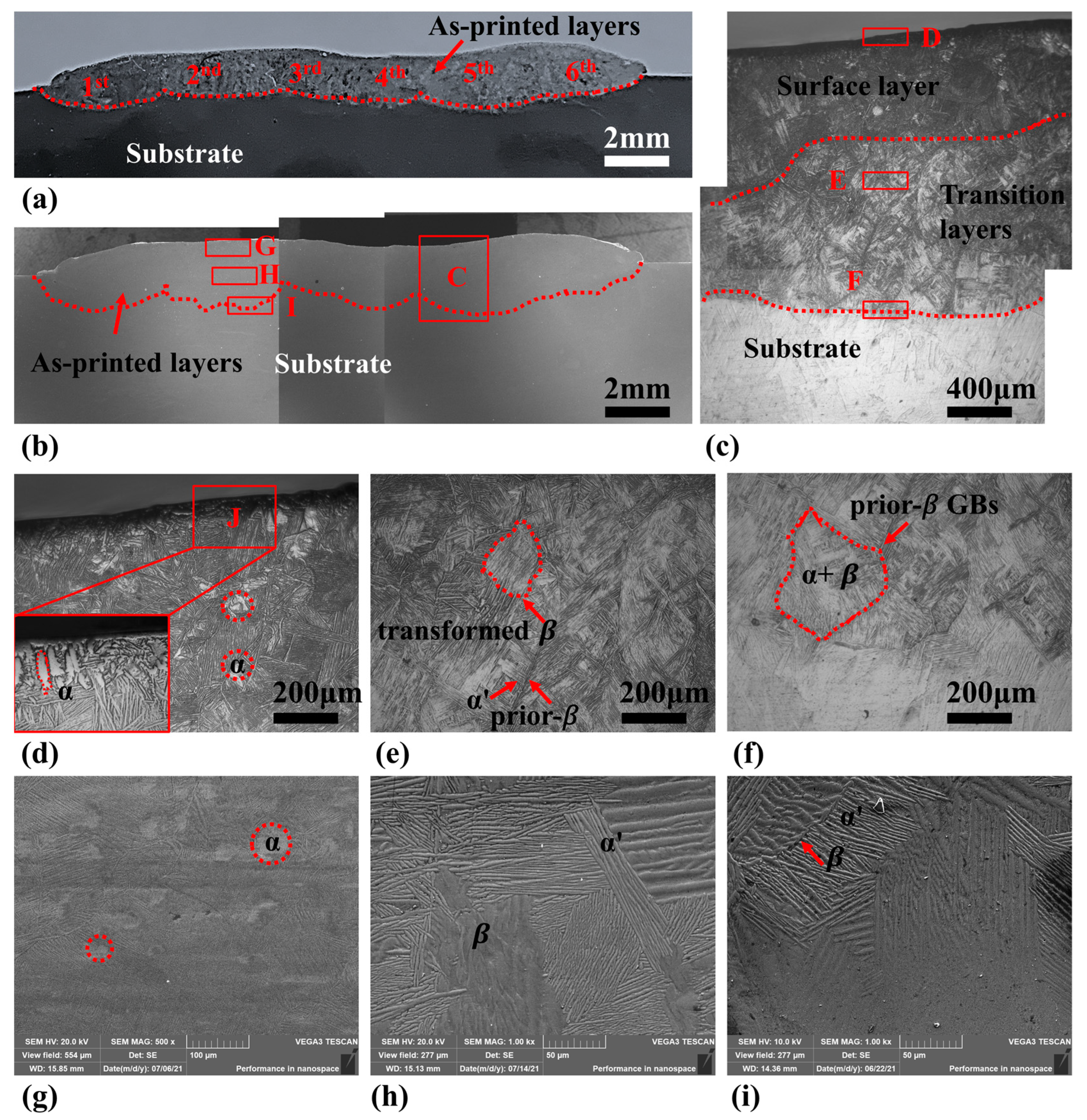
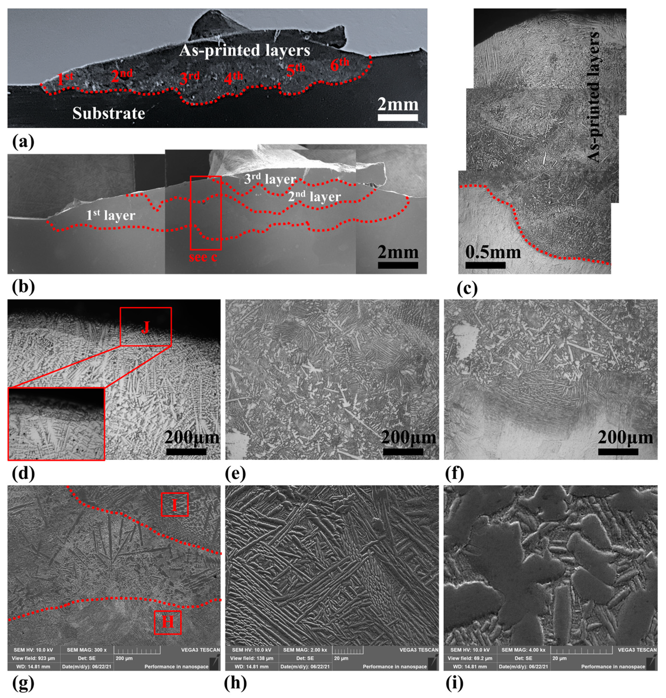
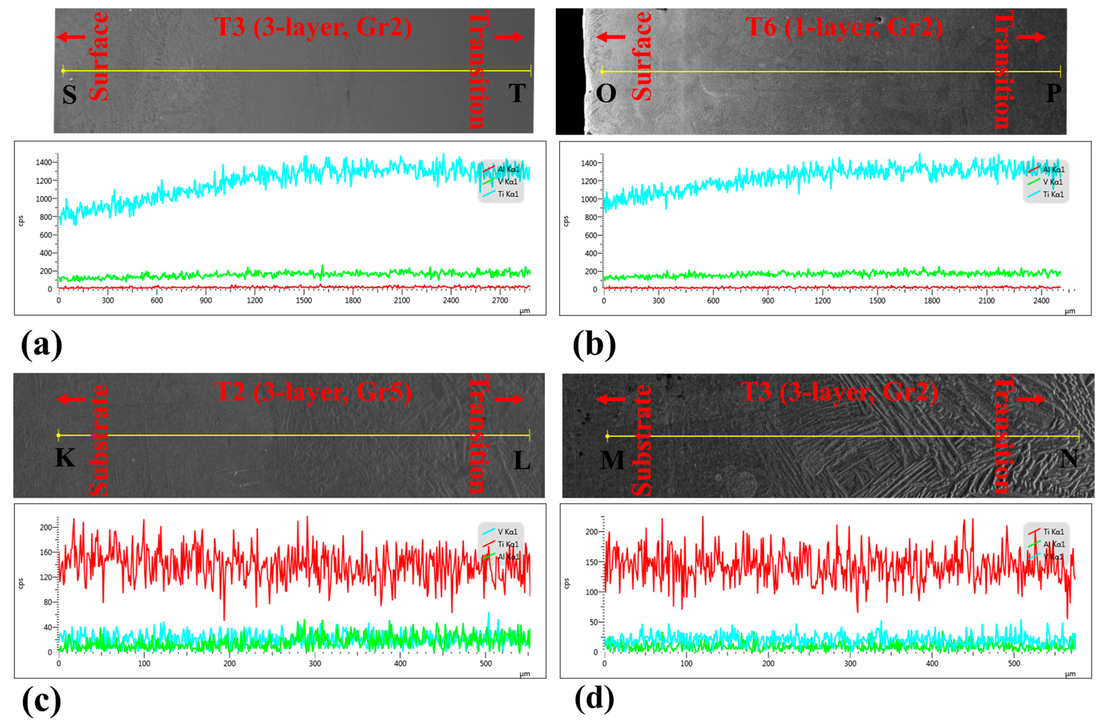
3.1. Geometry Formation and Defects

After additive manufacturing, the as–printed layers are evaluated for layer formation, incomplete fusion, microcracking, or possible cracks and porosity. Figure 2 shows the defects in the as–printed samples T1–T9 by X-ray radiography. Porosity (red circles in Figure 2a) and cracks (red arrows in Figure 2b) are typical defects. Samples T2 (three layer, Gr5) and T3 (three layer, G2) are whiter and brighter (black circles in Figure 2b,c) because multilayer additive manufacturing leads to greater sample thickness. The top layer, middle layer, and bottom layer can be observed in Figure 2c. For laser powers of 1.5 kW (T4) and 2.0 kW (T5), a lack of fusion (blue arrows in Figure 2d,e) is observed between adjacent tracks. When the laser power is increased to 2.5 kW (T6, Figure 2f) and 3.0 kW (T7, Figure 2g), the lack of fusion is no longer observed. A comparison of samples T8 and T6 shows that a slower scanning speed leads to excess additive (yellow arrow in Figure 2h). Excessive heat input increases the surface fluctuation of the samples, as the melting width and melting depth become too large. The geometry of the layer is found to be affected by the additives, number of layers, and laser parameters. The laser power influences the fusion of the additives, microcracking, and possible cracks. A greater scanning speed increases efficiency but with a higher risk of porosities and poor geometry formation.

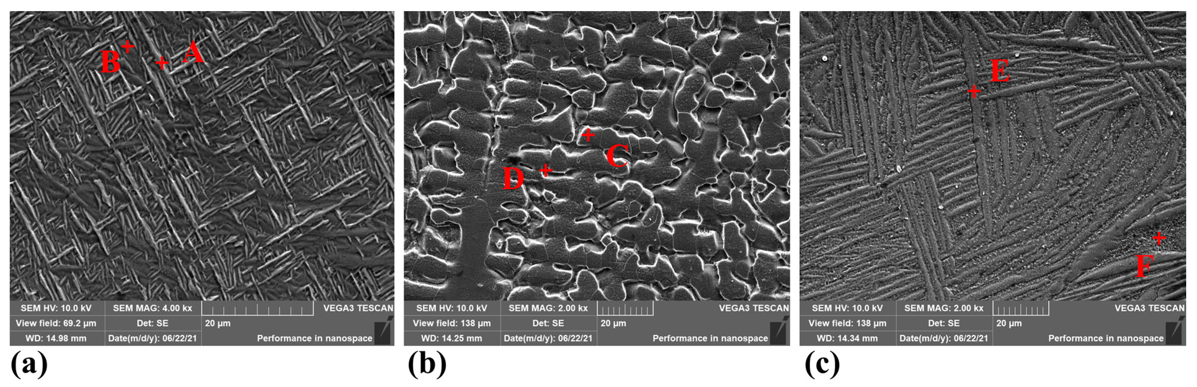
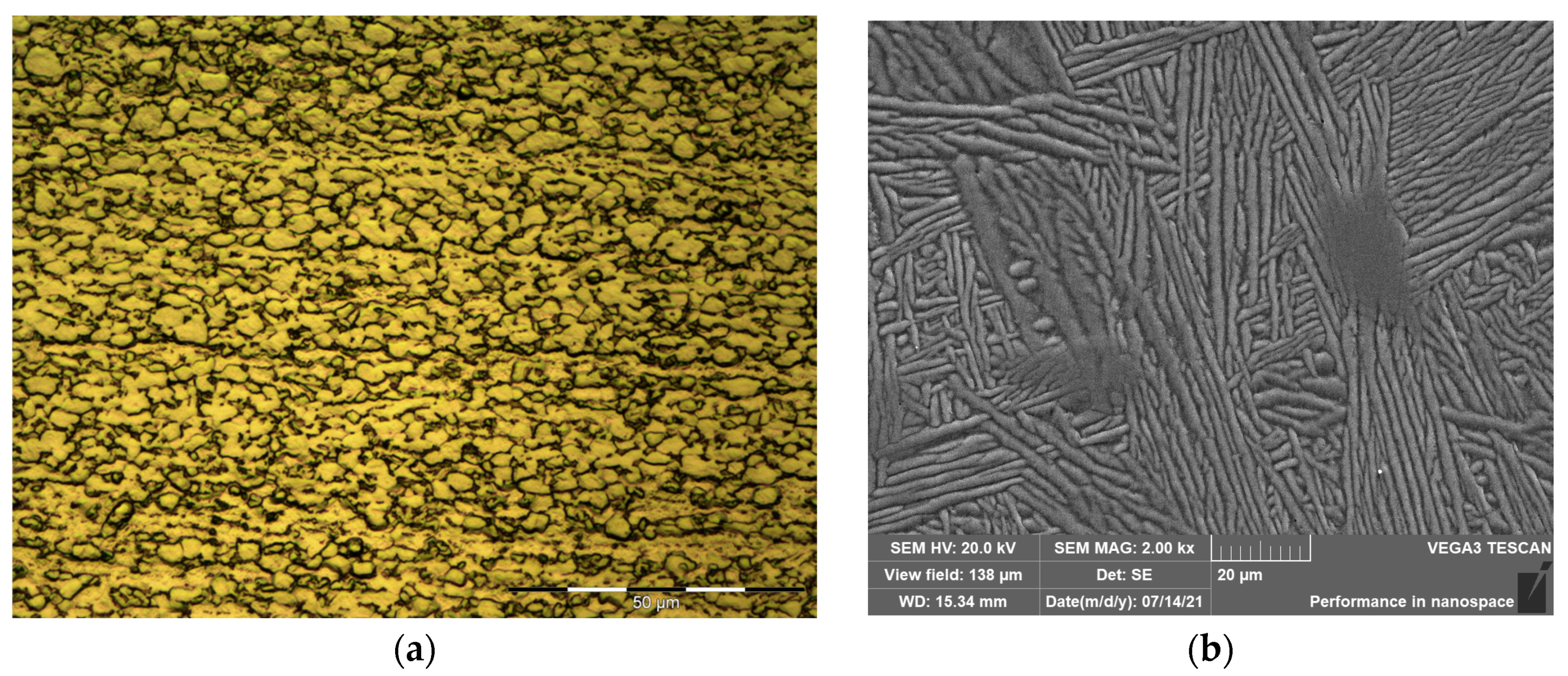
3.2. Microstructures and Phase Constituents

Figure 3a,b show the interface between the as–printed layers and the substrate under optical microscopy and scanning electron microscopy, respectively. The images are taken from the vertical cross–section of sample T6 (one layer; six passes). Figure 3a shows the first, second, third, fourth, fifth, and sixth passes from left to right. A thin surface layer, as highlighted by the dashed red lines, can be clearly distinguished as the interface between the as–printed layer and the substrate. The magnified image in Figure 3c shows the three typical regions: the surface region, transition region, and substrate. The microstructure in three regions, D, E, and F, is shown in Figure 3d, e, and f, respectively. The microstructure of the surface (region D in Figure 3c) consists of an α plate (white, slightly elongated grains; inset in Figure 3d), an acicular α′ martensite, residue β, and some equiaxed primary α phases. The lamellar layers are fine and closely arranged. As indicated by the red circles, more α was observed near the upper surface because of the additive Gr2 and oxygen–stabilized α formation. In the transition region (Figure 3e), the microstructure is consisted of transformed β that contains acicular α and α′, and α is at the transformed β grain boundaries. Coarser grains are observed at the interface of the additive layer and the substrate (Figure 3f). Figure 3g–i show scanning electron micrographs and the morphologies of regions G, H, and I in Figure 3b, respectively. Of the three regions, the lamellar structure in Figure 3i has the largest size.
Compared with the one–layer sample, the three–layer sample in Figure 4a,b shows a thicker additive layer and high dilution and exhibited a typical multilayer additive appearance. The first layer had six metal strips, the second layer had five metal strips, and the third layer had four metal strips. Since the additive metal strips that were stacked from bottom to top successively decreased (6–5–4), the shape of the as–printed layers appeared convex. Cracks are visible near the upper surface layer because of the multilayer thermal cycles. The microstructure in Figure 4c shows coarser α grains in an α′ martensite matrix. The microstructure in Figure 4c consists of three constituents: (1) residual β and strip α phases with dendritic growth formed near the upper surface (Figure 4d); (2) in the middle of the image, coarser needle–like α phase in a matrix of α′ martensite (Figure 4e); (3) the microstructure near the substrate is of the residual β and acicular α with the same orientation (Figure 4f). Therefore, the microstructure in the as–printed layers consists of different constituents of α (Ti–Al), (Ti–V), and α′ martensite. More martensitic microstructure and a greater level of residual stresses in the three–layer samples may have increased the embrittlement, which is suggested as the reasons for the cracks. In comparison with traditional powder–based or wire–based methods, the three–layer sample has a higher dilution due to a greater heat input. The laser power and laser scanning speed are the primary variables that control the dilution. In the present work, due to the fixture of the additive materials, the laser power and laser scanning speed control the amount of substrate that is melted and mixed in the pool.
Figure 5a–d show the diffusion (in–depth orientation) results of elemental titanium (Ti), aluminum (Al), and vanadium (V) in samples T2 (three layers, Gr5), T3 (three layers, Gr2), and T6 (one layer, Gr2). The energy dispersive X-ray spectroscopy (EDS) data for the labeled lines, ST, OP, KL, and MN, are shown in Table 3. In the 3 mm depth from the surface layers, Ti and V decreased to a 1.2 mm depth, and Al no longer varies. Near the as–printed layer/substrate interface, the Ti, Al, and V in samples T2 and T3 remained unchanged. Therefore, both the one– and three–layer samples have a 1.2 mm thick titanium depletion region.
As shown in Figure 6a and Table 3, EDS analysis of one of the fine acicular grains in sample T1 (indicated by A) shows that the bright grain is enriched with Ti, Al, and V and contains carbon. In addition to Ti, Al, V, and C, the neighboring matrix also contains oxygen (indicated by B). Therefore, the fine acicular phase is suggested as the α′ martensite in the β matrix. This matrix includes fine α. This result is attributed to grain refinement by laser–additive manufacturing. The faster cooling rate may have caused the acicular α to be finer than the original plate–like α. As shown in Figure 6b, the equiaxed grain (indicated by C) has a chemical composition of 99.93% Ti and 0.07% Al; therefore, the equiaxed grain is suggested as the α solid solution of Al in Ti. The matrix near α (indicated by D) contains 98.99% Ti, 0.06% Al, and 0.95% V, which is a solid solution of V in Ti (β). Figure 6c shows the coarser needle phase (indicated by E) and an intergranular phase (indicated by F). The former contains more oxygen, and the latter contains carbon. Oxygen–stabilized α and TiC are suggested to be these two phases.

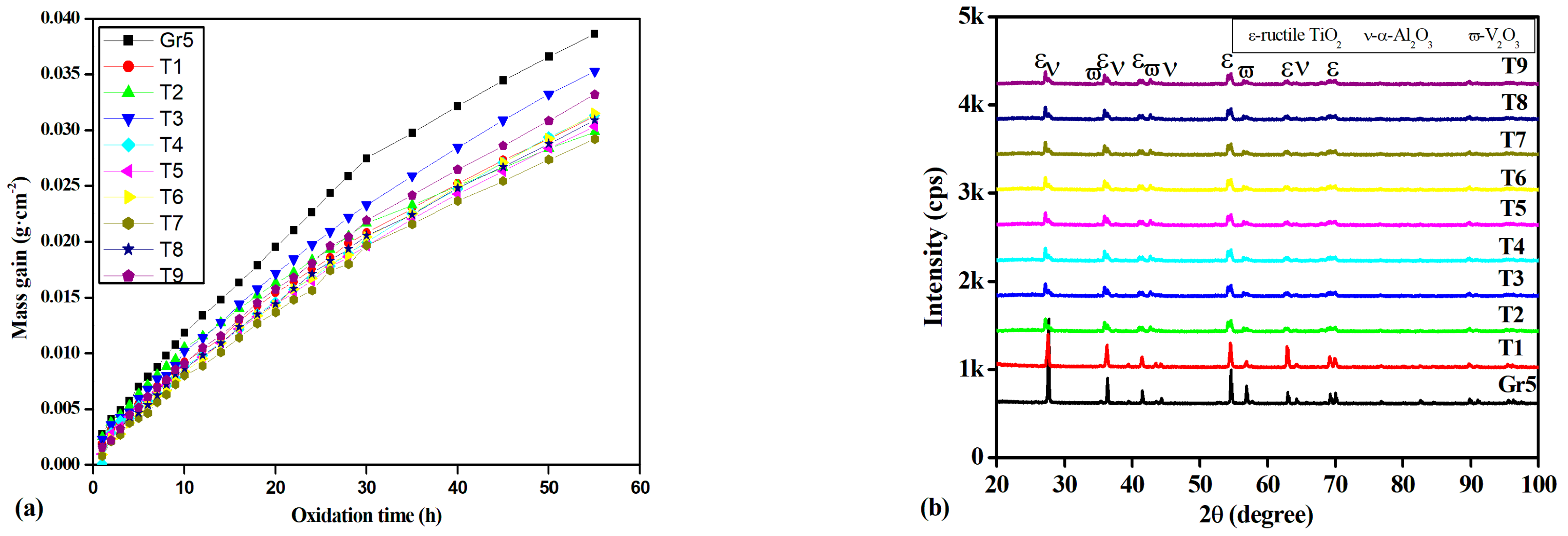
3.3. Oxide Resistance at 800 °C

Figure 7a shows the mass gain of the as–printed samples T1–T9 and the substrate over an extended time exposure (0–55 h) at 800 °C in air. The curves show the same trend in the mass change during high–temperature oxidation. Figure 7a shows that the oxidation mass gain rate of the substrate is higher than that of the as–printed samples T1–T9. The differences in oxidation resistance between the as–printed samples T1–T9 are smaller than those between the as–printed samples and the substrate.
Figure 7a shows that the oxidation resistance of the as–printed samples has changed with increasing laser power. The as–printed sample T7 (3 kW) exhibits the lowest mass gain per unit area. The mass gain per unit area of sample T6 (2.5 kW) is slightly lower than that of samples T4 (1.5 kW) and T5 (2.0 kW) during the early stage of oxidation. However, the mass gain per unit area is slightly higher than that of T5 and remains almost the same as that of T4 20 h later.
The as–printed sample T8 (3 mm·s−1) has a better oxidation resistance than samples T6 (6 mm·s−1) and T9 (9 mm·s−1). The mass gain per unit area of T6 is roughly the same as that of T8 within 35 h of the beginning of oxidation. However, T8 shows a better oxidation resistance after 35 h. The oxidation resistance of T9 is consistently lower than that of T6 and T8.
A comparison of the curves in Figure 7a shows that the mass gain per unit area of the samples with Gr2 (T3 and T6) as the additive material is lower than that of the sample with Gr5 (T1 and T2) as the additive material in the early stage. With increasing oxidation time, a reversed trend in the mass gain per unit area is observed for the one– and three–layer samples. However, the reversal occurred in approximately 45 h for the one–layer sample, whereas it occurred in approximately 16 h for the three–layer sample.
Specimens from the oxidized surface of the substrate Gr5 titanium and the as–printed samples T1–T9 are analyzed by XRD for crystal structures, as shown in Figure 7b. The primary phase identified is TiO2. The observed peaks such as (110), (101), and (211) are the typical three strong peaks of rutile titanium dioxide. In addition to TiO2, Al2O3 and V2O3 are also observed in the oxidized surface of the as–printed layers. A clear peak widening is observed for the as–printed samples T1–T9 compared with the substrate. Peak widening is due to grain refinement. Compared with the Gr5 substrate, the peaks of the crystal plane (111) of the deposit layers shifted to the left.

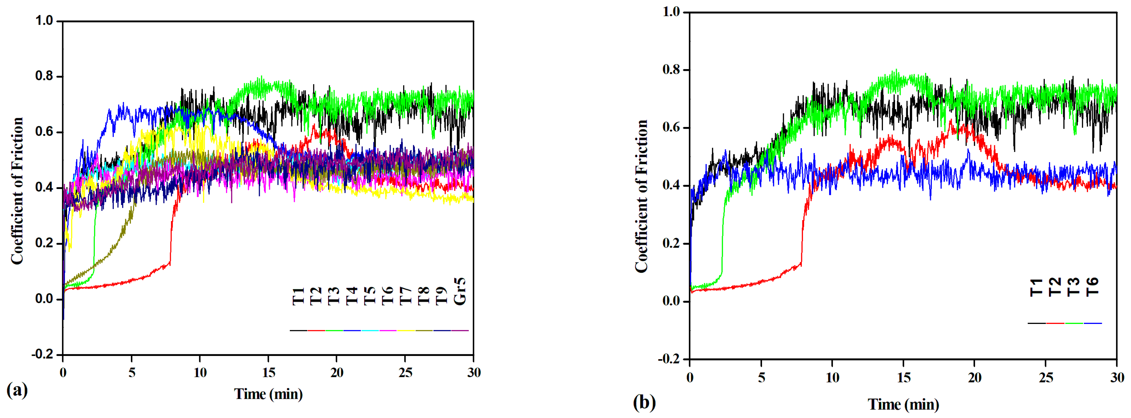
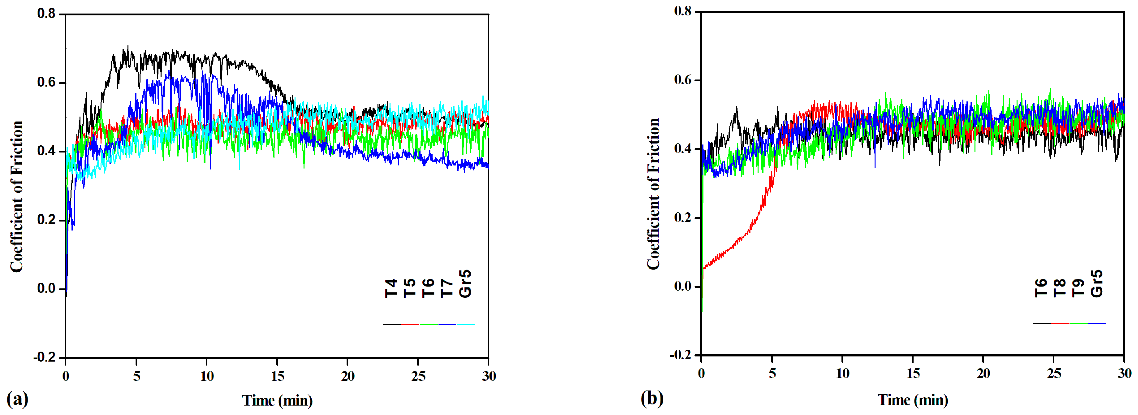
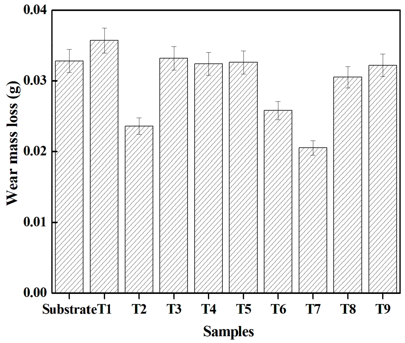
3.4. Wear Resistance

The wear resistance of different as–printed samples was examined by dry sliding tests. Figure 8a shows the COF variations in the Gr5 substrate and as–printed samples T1–T9 after dry friction for 30 min with a GCr15 steel (high–carbon chromium bearing steel) friction pair at room temperature. In comparison with the substrate (Gr5), the as–printed samples have a lower COF, except samples T1 and T3. The results also indicate that samples T7, T2, and T6 have the lowest COF; T4, T5, T8, and T9 have average COF; and samples T1 and T3 have the highest COF.
Figure 8b shows that after the running–in period, increasing the number of layers reduced the COF of the additive sample with Gr5 additive strips, while the opposite was observed for the sample with Gr2 additive strips. In comparison with T1 (single layer, Gr5) and T3 (three layers, Gr2) samples, sample T6 (single layer, Gr2) and sample T2 (three layers, Gr5) exhibited better wear resistance.

4. Discussion

4.1. Effect of Processing Conditions on the Oxidation Resistance

The improved resistance to oxidation makes titanium a better fit for lightweight applications such as in the aerospace and automotive industries [39]. The results in Figure 7a show that the as–printed titanium alloys have better oxidation resistance after laser processing.
The phase–oxide mechanism and active–passive transition region corresponding to the passivation process are believed to be the oxidation–resistance mechanism [40,41]. First, increasing the laser power is helpful for oxidation resistance due to the phase–oxide mechanism. However, the loss of alloy elements due to a high heat input from the laser power reduces the oxidation resistance. Therefore, the oxidation resistance did not show a positive correlation with the laser power. Second, additive materials play a key role in the oxidation resistance of as–printed samples. Grade 5 titanium alloy has an excellent oxidation resistance in air or in liquid [42], and it shows a better oxidation resistance after laser scanning. Third, a fast laser scanning speed (9 mm·s−1) lowers the oxidation resistance of as–printed samples. Sample T7 has better oxidation resistance when using the optimized processing conditions: laser power: 3.0 kW; scanning speed: 6 mm·s−1.

4.2. Effect of Processing Conditions on the Wear Resistance

The results in Figure 9a show the influence of the laser power on the wear resistance of the as–printed samples. When the laser power was 1.5 and 2.0 kW, the final COF of the samples was 0.5 and 0.48, respectively—approximately equal to the 0.49 value of the Gr5 substrate. When the laser power increased to 2.5 and 3.0 kW, the final COF was 0.43 and 0.38, respectively, which is significantly lower than the friction coefficient of the Gr5 substrate and has a better wear resistance. However, as indicated in Figure 8a, although the laser power for samples T1 and T3 was 2.5 kW, neither of them obtained a better wear resistance. Therefore, according to the coefficient of friction and the mass losses, a high laser power, reasonable scanning speed, and cross–hatching strategy were confirmed to be essential to achieve minimal metallurgical defects and full densification. When the laser power was too high (3 kW) or too low (1.5 kW), the friction coefficient of the sample in the running–in period was much higher than that after stability was reached. Figure 9b shows the COF variation when the scanning speeds were 3 mm·s−1 (T8), 6 mm·s−1 (T6), and 9 mm·s−1 (T9). It can be seen that the COF first decreased and then increased with the decreased scanning speed, and the T6 sample, for which the scanning speed was 6 mm·s−1, had the best wear resistance.
Figure 10 shows a comparison of the wear mass losses in the as–printed samples and the Gr5 substrate. The results show that the wear mass loss of the substrate was nearly 37% more than that of sample T7. Except for samples T2, T6 and T7, the wear mass losses of the other samples are not much different from those of the substrate.
As shown in Figure 11, the Gr5 titanium alloy substrate material contains bright α and dark β phases. After laser–additive manufacturing, martensitic α′ is the predominant phase. The phase transformation is affected by the cooling rate through the laser scanning speed [43]. The formation of martensitic α′ is one of the reasons for the improvement of the wear resistance.
As summarized in the Introduction, methods of preparation were proposed for surface modification (Denlinger et al. [19], Zykova et al. [44], Obadele et al. [45], Wang et al. [46], Deepak et al. [47], and Farabi et al. [48]). As indicated in Table 4, the methods include laser DED, electron–beam additive manufacturing (EBMA), laser cladding, heat treatment, nitrogen treatment, and additive friction stir deposition. The performance parameters include wear, oxidation resistance, residual stress and distortion, strength, hardness, and corrosion resistance. Compared with the previously reported additive layers, the as–fabricated samples prepared in this work showed a better wear resistance and a higher oxidation resistance: the lowest COF of the laser DED samples decreased by 22.4% compared with that of the substrate, and the mass gain per unit area of most samples was 26.3% lower than that of the substrate at 800 °C. The proposed pre–placed metal–strip–based laser–additive manufacturing method allows for the custom design of additive materials, which is also simpler, more flexible and feasible.

5. Conclusions

The laser–additive manufacturing process based on a pre–placed metal strip can be used to fabricate as–printed layers on a titanium substrate. The additive fixation problem was solved by a pre–placed metal strip with the help of resistant spot welding. The proposed pre–placed metal–strip–based laser–additive manufacturing method allows researchers and engineers to design custom additive materials
Microcracking and porosity are major challenges during the laser–additive manufacturing process. Inappropriate laser parameters, an excessive gap between metal strips, and the detachment of the pre–placed metal strip joints led to pore formation. Cracks appeared during the cooling of the three–layer samples because the increasing internal stress exceeded the tensile strength of the titanium alloy. Crack formation can be prevented by preheating the substrate and reducing the cooling rate.
The microstructure in the as–printed layers included α′ martensite, oxygen–stabilized α, transformed β that contained coarse and fine acicular α, residual β, prior β grain boundaries, and impurities. The sample T7 has better oxidation resistance when using the following processing conditions: laser power: 3.0 kW; scanning speed: 6 mm·s−1.

Author Contributions

J.L., J.W., B.L. and C.X.: conceptualization, investigation, methodology, software, formal analysis, writing—original draft preparation, and visualization; P.X.: supervision, writing—review and editing, and project administration; L.L., B.C. and P.X.: writing—review and editing. All authors have read and agreed to the published version of the manuscript.

Funding

This research was funded by the Natural Science Foundation of Shanghai (grant number: 20ZR1422700) and the Class III Peak Discipline of Shanghai—Materials Science and Engineering (High–Energy Beam Intelligent Processing and Green Manufacturing).

Data Availability Statement

Not applicable.

Conflicts of Interest

The authors declare no conflict of interest.

References

  1. Wang, Z.; Yang, S.; Peng, Z.; Gao, Z. Effect of defects in laser selective melting of Ti–6Al–4V alloy on microstructure and mechanical properties after heat treatment. Opt. Laser Technol. 2022, 156, 108522. [Google Scholar] [CrossRef]
  2. Zhang, Z.; Ma, P.; Fang, Y.; Yang, Z.; Zhang, N.; Prashanth, K.G.; Jia, Y. Effect of NiCoFeAlTi high entropy intermetallic reinforcement particle size on the microstructure and mechanical properties of CoCrFeMnNi high–entropy alloy composites fabricated by selective laser melting. J. Alloys Compd. 2023, 947, 169417. [Google Scholar] [CrossRef]
  3. Zhao, F.; Qin, Y.; Zhang, D.; Liang, M. Effect of filler wire on laser lap welding of Al–Si coated 22MnB5 hot stamping steel. J. Mater. Eng. Perform. 2022, 31, 9670–9680. [Google Scholar] [CrossRef]
  4. Liang, M.; Qin, Y.; Zhang, D.; Zhao, F. Microstructural evolution and mechanical properties of vacuum brazed TC4 titanium alloy joints with Ti–Zr–Ni filler metal. J. Mater. Eng. Perform. 2022, 31, 9340–9348. [Google Scholar] [CrossRef]
  5. Ma, S.; Li, B.; Ma, Y.; Zhang, P.; Xu, P. Effect of brazing filler metals and welding parameters on laser welding–brazing joints of WC–Co to S1045. Metals 2022, 12, 1780. [Google Scholar] [CrossRef]
  6. Ji, J.; Zhang, Z.; Chen, J.; Zhang, H.; Zhang, Y.; Lu, H. Effect of refractory elements M (=Re, W, Mo or Ta) on the diffusion properties of boron in nickel–based single crystal superalloys. Vacuum 2023, 211, 111923. [Google Scholar] [CrossRef]
  7. Zhang, T.; Yu, H.; Li, Z.; Kou, S.; Kim, H.J.; Tillmann, W. Progress on effects of alloying elements on bainite formation and strength and toughness of high strength steel weld metal. Mater. Res. Express 2021, 8, 032002. [Google Scholar] [CrossRef]
  8. Zhang, T.; Wang, W.; Ma, Y.; Fang, N.; Lin, S.; Li, Z.; Kou, S. In situ observation of microstructural and inclusions evolution in high–strength steel deposited metals with various rare earth Pr contents. Materials 2022, 15, 1257. [Google Scholar] [CrossRef]
  9. Zhang, Y.; Chen, J.; Zhang, W.; Li, C.; Qiu, C.; Ding, J.; Lu, H.; Zhang, K. Study of spatter net forming mechanism and penetration mode under flexible ring mode laser welding. J. Mater. Res. Technol. 2023, 24, 2213–2225. [Google Scholar] [CrossRef]
  10. Fan, C.; Yang, S.; Duan, C.; Zhu, M.; Bai, Y. Microstructure and mechanical properties of 6061 aluminum alloy laser–MIG hybrid welding joint. J. Cent. South Univ. 2022, 29, 898–911. [Google Scholar] [CrossRef]
  11. Zhang, P.; Wang, J.; Zhang, F.; Xu, P.; Li, L.; Li, B. Design and analysis of welding inspection robot. Sci. Rep. 2022, 12, 22651. [Google Scholar] [CrossRef] [PubMed]
  12. Hartbower, C.E.; Orner, G.M. Technical Report: Feasibility of Titanium for Welded Missiles; Report No.: WAL–TR–401/301; United States Department of Energy, Office of Scientific and Technical Information: Washington, DC, USA, 1958.
  13. Afanas’ev, V.A.; Nikitin, P.V.; Tushavina, O.V. Behavior of titanium alloys in aerodynamic heating of hypersonic airplanes. Russ. Eng. Res. 2019, 39, 25–30. [Google Scholar] [CrossRef]
  14. Tobe, H.; Matsuki, Y.; Takeuchi, S.; Sato, E. Deployable rocket nozzle utilizing superelastic titanium alloy sheet. Mater. Trans. 2020, 61, 68–71. [Google Scholar] [CrossRef]
  15. Prestat, M.; Thierry, D. Corrosion of titanium under simulated inflammation conditions: Clinical context and in vitro investigations. Acta Biomater. 2021, 136, 72–87. [Google Scholar] [CrossRef] [PubMed]
  16. Bai, H.Q.; Zhong, L.S.; Kang, L.; Liu, J.B.; Zhuang, W.J.; Lv, Z.L.; Xu, Y.H. A review on wear–resistant coating with high hardness and high toughness on the surface of titanium alloy. J. Alloys Compd. 2021, 882, 160645. [Google Scholar] [CrossRef]
  17. Kruth, J.P.; Leu, M.C.; Nakagawa, T. Progress in additive manufacturing and rapid Prototyping. CIRP Ann.–Manuf. Technol. 1998, 47, 525–540. [Google Scholar] [CrossRef]
  18. Beese, A.M.; Carroll, B.E. Review of mechanical properties of Ti–6Al–4V made by laser–based additive manufacturing using powder feedstock. JOM 2016, 68, 724–734. [Google Scholar] [CrossRef]
  19. Denlinger, E.R.; Heigel, J.C.; Michaleris, P.; Palmer, T.A. Effect of inter–layer dwell time on distortion and residual stress in additive manufacturing of titanium and nickel alloys. J. Mater. Process. Technol. 2015, 215, 123–131. [Google Scholar] [CrossRef]
  20. Ghouse, S.; Babu, S.; Nai, K.; Hooper, P.A.; Jeffers, J.R.T. The influence of laser parameters, scanning strategies and material on the fatigue strength of a stochastic porous structure. Addit. Manuf. 2018, 22, 290–301. [Google Scholar] [CrossRef]
  21. Wang, C.; Suder, W.; Ding, J.; Williams, S. The effect of wire size on high deposition rate wire and plasma arc additive manufacture of Ti–6Al–4V. J. Mater. Process. Technol. 2021, 288, 116842. [Google Scholar] [CrossRef]
  22. Murr, L.E.; Gaytan, S.M.; Ceylan, A.; Martinez, E.; Martinez, J.L.; Hernandez, D.H.; Machado, B.I.; Ramirez, D.A.; Medina, F.; Collins, S.; et al. Characterization of titanium aluminide alloy components fabricated by additive manufacturing using electron beam melting. Acta Mater. 2010, 58, 1887–1894. [Google Scholar] [CrossRef]
  23. Juechter, V.; Scharowsky, T.; Singer, R.F.; Körner, C. Processing window and evaporation phenomena for Ti–6Al–4V produced by selective electron beam melting. Acta Mater. 2014, 76, 252–258. [Google Scholar] [CrossRef] [Green Version]
  24. Karlsson, J.; Norell, M.; Ackelid, U.; Engqvist, H.; Lausmaa, J. Surface oxidation behavior of Ti–6Al–4V manufactured by Electron Beam Melting (EBM®). J. Manuf. Process. 2015, 17, 120–126. [Google Scholar] [CrossRef]
  25. Bambach, M.; Sizova, I.; Sydow, B.; Hemes, S.; Meiners, F. Hybrid manufacturing of components from Ti–6Al–4V by metal forming and wire–arc additive manufacturing. J. Mater. Process. Technol. 2020, 282, 116689. [Google Scholar] [CrossRef]
  26. Soro, N.; Saintier, N.; Attar, H.; Dargusch, M.S. Surface and morphological modification of selectively laser melted titanium lattices using a chemical post treatment. Surf. Coat. Technol. 2020, 393, 125794. [Google Scholar] [CrossRef]
  27. Thijs, L.; Verhaeghe, F.; Craeghs, T.; Humbeeck, J.V.; Kruth, J.P. A study of the microstructural evolution during selective laser melting of Ti–6Al–4V. Acta Mater. 2010, 58, 3303–3312. [Google Scholar] [CrossRef]
  28. Hollander, D.A.; Walter, M.; Wirtz, T.; Sellei, R.; Schmidt–Rohlfing, B.; Paar, O.; Erli, H.J. Structural, mechanical and in vitro characterization of individually structured Ti–6Al–4V produced by direct laser forming. Biomaterials 2006, 27, 955–963. [Google Scholar] [CrossRef] [PubMed]
  29. Verma, P.K.; Warghane, S.; Nichul, U.; Kumar, P.; Dhole, A.; Hiwarkar, V. Effect of boron addition on microstructure, hardness and wear performance of Ti–6Al–4V alloy manufactured by laser powder bed fusion additive manufacturing. Mater. Charact. 2021, 172, 110848. [Google Scholar] [CrossRef]
  30. Lu, L.; Fuh, J.Y.H.; Chen, Z.D.; Leong, C.C.; Wong, Y.S. In situ formation of TiC composite using selective laser melting. Mater. Res. Bull. 2000, 35, 1555–1561. [Google Scholar] [CrossRef]
  31. Guo, W.; Wang, H.; Peng, P.; Song, B.W.; Zhang, H.Q.; Shao, T.W.; Huan, H.; Qiao, H.C.; Qu, G.D.; Zhu, D.Z.; et al. Effect of laser shock processing on oxidation resistance of laser additive manufactured Ti6Al4V titanium alloy. Corros. Sci. 2020, 170, 108655. [Google Scholar] [CrossRef]
  32. Fox, P.; Pogson, S.; Sutcliffe, C.J.; Jones, E. Interface interactions between porous titanium/tantalum coatings, produced by Selective Laser Melting (SLM), on a cobalt–chromium alloy. Surf. Coat. Technol. 2008, 202, 5001–5007. [Google Scholar] [CrossRef]
  33. Dutta, B.; Froes, F.H.S. 24–The additive manufacturing (AM) of titanium alloys. In Titanium Powder Metallurgy; Qian, M., Froes, F.H.S., Eds.; Butterworth–Heineman: Oxford, UK, 2015; pp. 447–468. [Google Scholar]
  34. Trevisan, F.; Calignano, F.; Aversa, A.; Marchese, G.; Lombardi, M.; Biamino, S.; Ugues, D.; Manfredi, D. Additive manufacturing of titanium alloys in the biomedical field: Processes, properties and applications. J. Appl. Biomater. Func. 2018, 16, 57–67. [Google Scholar] [CrossRef] [PubMed]
  35. Tapoglou, N.; Clulow, J.; Curtis, D. Increased shielding of a direct energy deposition process to enable deposition of reactive materials; an investigation into deposition of 15–5 PH stainless steel, Inconel 718 and Ti–6Al–4V. CIRP J. Manuf. Sci. Technol. 2022, 36, 227–235. [Google Scholar] [CrossRef]
  36. Kelly, C.N.; Kahra, C.; Maier, H.J.; Gall, K. Processing, structure, and properties of additively manufactured titanium scaffolds with gyroid–sheet architecture. Addit. Manuf. 2021, 41, 101916. [Google Scholar] [CrossRef]
  37. Moghimian, P.; Poirié, T.; Habibnejad–Korayem, M.; Zavala, J.A.; Kroeger, J.; Marion, F.; Larouche, F. Metal powders in additive manufacturing: A review on reusability and recyclability of common titanium, nickel and aluminum alloys. Addit. Manuf. 2021, 43, 102017. [Google Scholar] [CrossRef]
  38. Amado, J.M.; Rodríguez, A.; Montero, J.N.; Tobar, M.J.; Yáñez, A. A comparison of laser deposition of commercially pure titanium using gas atomized or Ti sponge powders. Surf. Coat. Technol. 2019, 374, 253–263. [Google Scholar] [CrossRef]
  39. Chakraborty, D.; Tirumala, T.; Chitral, S.; Sahoo, B.N.; Kiran, D.V.; Kumar, P.A. The state of the art for wire arc additive manufacturing process of titanium alloys for aerospace applications. J. Mater. Eng. Perform. 2022, 31, 6149. [Google Scholar] [CrossRef]
  40. Tshephe, T.S.; Akinwamide, S.O.; Olevsky, E.; Olubambi, P.A. Additive manufacturing of titanium–based alloys—A review of methods, properties, challenges, and prospects. Heliyon 2022, 8, e09041. [Google Scholar] [CrossRef]
  41. Mordyuk, B.N.; Voloshko, S.M.; Zakiev, V.I.; Burmak, A.P.; Mohylko, V.V. Enhanced resistance of Ti6Al4V alloy to high–temperature oxidation and corrosion by forming alumina composite coating. J. Mater. Eng. Perform. 2021, 30, 1780. [Google Scholar] [CrossRef]
  42. Pitchi, C.S.; Priyadarshini, A.; Narala, S.K.R. Influence of cooling kinetics on surface texture, hydrophilicity and scratch resistance of the oxide layers produced by thermal oxidation on Ti–6Al–4V. Surf. Coat. Technol. 2022, 450, 128956. [Google Scholar] [CrossRef]
  43. Xu, P.Q.; Li, L.; Zhang, C.S. Microstructure characterization of laser welded Ti–6Al–4V fusion zones. Mater. Charact. 2014, 87, 179–185. [Google Scholar] [CrossRef]
  44. Zykova, A.; Vorontsov, A.; Nikolaeva, A.; Chumaevskii, A.; Kalashnikov, K.; Gurianov, D.; Savchenko, N.; Nikonov, S.; Kolubaev, E. Structural design and performance evaluation of Ti6Al4V/5%Cu produced by electron–beam additive technology with simultaneous double–wire feeding. Mater. Lett. 2022, 312, 131586. [Google Scholar] [CrossRef]
  45. Obadele, B.A.; Olubambi, P.A.; Andrews, A.; Pityana, S.; Mathew, M.T. Electrochemical behaviour of laser–clad Ti6Al4V with CP Ti in 0.1 M oxalic acid solution. J. Alloys Compd. 2015, 646, 753–759. [Google Scholar] [CrossRef]
  46. Wang, Y.; Hao, E.; Zhao, X.; Xue, Y.; An, Y.; Zhou, H. Effect of microstructure evolution of Ti6Al4V alloy on its cavitation erosion and corrosion resistance in artificial seawater. J. Mater. Sci. Technol. 2022, 100, 169–181. [Google Scholar] [CrossRef]
  47. Deepak, J.R.; Joy, N.; Krishnamoorthy, A.; Jaswanth, C.P.; Harish, G. Gas nitriding of CP grade–2 commercially pure titanium and Ti6Al4V grade–5 titanium alloy. Mater. Today Proc. 2021, 44, 3744–3750. [Google Scholar] [CrossRef]
  48. Farabi, E.; Babaniaris, S.; Barnett, M.R.; Fabijanic, D.M. Microstructure and mechanical properties of Ti6Al4V alloys fabricated by additive friction stir deposition. Addit. Manuf. Lett. 2022, 2, 100034. [Google Scholar] [CrossRef]
Figure 1. Schematics of the metal–strip–based laser–additive manufacturing setup. (a) Pre–placed metal strip fixture. (b) The experimental setup for laser–additive manufacturing. (c) Samples in the gas shield chamber and (d) after laser–additive manufacturing.
Metals 13 01372 g001
Figure 2. Defect examination for the as–printed samples of (a) T1, (b) T2, (c) T3, (d) T4, (e) T5, (f) T6, (g) T7, (h) T8, and (i) T9 by X-ray radiography. Cracks can be seen on the upper surface of T2 (b), which was prepared using multilayer additives.
Metals 13 01372 g002
Figure 3. A cross–sectional image of the as–printed sample T6 (1 layer) on a titanium substrate using (a) optical microscopy and (b) scanning electron microscopy. (c) A magnified optical image showing the surface layer, transition layer, and substrate. Magnified microstructures of (d) region D; the inset shows the microstructures of upper surface region J, (e) region E, and (f) region F in (c). SEM images showing the microstructures and morphologies of (g) region G, (h) region H, and (i) region I in (b).
Metals 13 01372 g003
Figure 4. A cross–sectional image of the as–printed samples T2 (three–layer) on a titanium substrate using (a) optical microscopy and (b) scanning electron microscopy. (c) A magnified optical image showing the as–printed layers and the interfaces of the as–printed layers and substrate. Magnified microstructures of (d) region D, (e) region E, and (f) region F in (c). (g) SEM image of the as–printed layer/substrate interface; magnified image of (h) region H and (i) region I in (g).
Metals 13 01372 g004
Figure 5. Line scan results of Ti, Al, and V diffusion (a) near the surface layer (in–depth orientation) in samples T3 (three layers) and (b) T6 (1 layer) using Gr2 as additive. (c) Near the as–printed layer/substrate interface (in depth orientation) in samples T2 (Gr5) and (d) T3 (Gr2) with three–layers. The EDS of the labeled ST, OP, KL, and MN lines are shown in Table 3.
Metals 13 01372 g005
Figure 6. EDS analysis of the labeled locations given in Table 3. (a) Sample T1, (b) Sample T2, and (c) Sample T6.
Metals 13 01372 g006
Figure 7. Oxidation resistance. (a) Mass gain vs. time plots for as–printed layers T1–T9 and Gr5 substrate. (b) X-ray diffraction pattern.
Metals 13 01372 g007
Figure 8. Wear resistance of (a) Gr5 substrate and as–printed samples T1–T9. (b) One–layer samples: T1 (one layer, Gr5) and T6 (one layer, Gr2) and three–layer samples: T2 (three layers, Gr5) and T3 (three layers, Gr2).
Metals 13 01372 g008
Figure 9. COF obtained for (a) T4 (1.5 kW), T5 (2.0 kW), T6 (2.5 kW), T7 (3.5 kW), and Gr5 substrate. (b) T6 (6 mm·s−1), T8 (3 mm·s−1), T9 (9 mm·s−1), and Gr5 substrate.
Metals 13 01372 g009
Figure 10. Comparison of wear mass losses in the as–printed samples and the Gr5 substrate.
Metals 13 01372 g010
Figure 11. Typical microstructures of Gr5 titanium alloy: (a) before laser–additive manufacturing; (b) after laser–additive manufacturing.
Metals 13 01372 g011
Table 1. Chemical composition (wt %) of commercially pure Grade 2 titanium (Gr2) and Grade 5 titanium (Gr5).
ElementSubstrateAdditives (Metal Strips)
Gr5Gr2Gr5
Iron (Fe)0.40.30 max0.4
Oxygen (O)0.20.25 max0.2
Carbon (C)0.10.08 max0.1
Aluminum (Al)5.5–6.755.5–6.75
Nitrogen (N)0.050.03 max0.05
Vanadium (V)3.5–4.53.5–4.5
Hydrogen (H)0.01250.015 max0.0125
Titanium (Ti)RemainderRemainderRemainder
Table 2. Laser parameters on Gr5 titanium substrate with pre–placed Gr5 and Gr2 metal strips as additives; the size of the metal strips was 100 mm × 3 mm × 1 mm.
SamplesSubstrateAdditive (Metal Strips)LayersPassesLaser Power
(kW)
Scanning Speed
(mm·s−1)
P1Gr5Gr21121.56
P21122.56
P3112.56
P4112.58
P5112.56
P6112.58
T1Gr5Gr5162.56
T2Gr5Gr5162.56
262.56
362.56
T3Gr5Gr2162.56
262.56
362.56
T4Gr5Gr2161.56
T5162.06
T6162.56
T7163.06
T8162.53
T9162.59
Table 3. EDS–determined chemical compositions of locations labeled in Figure 5 and Figure 6. Carbon and oxygen values are only qualitative, i.e., indicating the existence, not the exact amount.
SamplesTitaniumAluminumVanadiumCarbonSiliconOxygenOmitted
(at %)(wt %)(at %)(wt %)(at %)(wt %)(at %)(wt %)(at %)(wt %)(at %)(wt %)
A–T1(85.15)(91.68)(6.26)(3.80)(2.52)(2.89)(6.07)(1.64)
B–T1(77.84)(89.32)(6.34)(4.10)(1.24)(1.51)(5.36)(1.54)(9.22)(3.53)
C–T3(99.93)(99.96)(0.07)(0.04)
D–T3(98.99)(98.96)(0.06)(0.03)(0.95)(1.01)
E–T6(74.33)(90.05)(0.15)(0.10)(0.11)(0.14)(8.42)(2.56)(0.90)(0.64)(16.09)(6.51)
F–T6(60.73)(85.64)(0.40)(0.32)(37.95)(13.42)Na
KL–T2(83.46)(92.95)(2.01)(1.26)(0.97)(1.15)(4.39)(1.22)(9.17)(3.41)
MN–T3(93.68)(97.71)(0.37)(0.22)(0.61)(0.68)(5.33)(1.40)
OP–T6(90.87)(97.16)(0.47)(0.28)(0.27)(0.31)(8.4)(2.25)
ST–T3(86.39)(95.96)(0.35)(0.22)(0.14)(0.16)(13.12)(3.66)
Table 4. Comparison of methods and mechanical properties of as–fabricated samples between this work and reported references.
SubstrateDeposited MetalsMethods of PreparationMechanical PropertiesPerformanceReferences
Gr5Gr5
Gr2
Laser DEDWear and
oxidation
The lowest COF of laser DED sample decreased by 22.4% compared with substrate.
The mass gain per unit area of most samples was 26.3% lower than that of the substrate at 800 °C.
This work
Gr5Gr5Laser DEDResidual stress
and distortion
Longer dwell times led to greater residual stress and deformation.(Ref. [8])
Gr2Gr5 with 5% CuEBAMStrengthThe tensile strength increased by about 20%, and the tensile strain decreased by 3 times.(Ref. [32])
Gr5Gr2Laser claddingHardness and corrosion resistanceWithin the scanning speed range of 0.4–0.8 m/min, the hardness value increased, and the corrosion current densities decreased as scan speed decreased.(Ref. [33])
Gr5Heat treatmentMicrohardness
and corrosion resistance
Furnace–cooling–TC4 microhardness: 28% higher
Air–cooling–TC4 microhardness: 75% higher
Corrosion resistance: air–cooling–TC4 > TC4 > furnace–cooling–TC4.
(Ref. [34])
Gr2
Gr5
Nitrogen treatmentHardnessGr2 hardness increased by 3 times, and Gr5 hardness was 11% higher.
Gr2 nitrided thickness: 2.001 µm.
Gr5 nitrided thickness: 2.604 µm.
(Ref. [35])
Gr5Gr5Additive friction stir depositionStrengthDuctility: 20%.
Yield strength: 1010 MPa.
Tensile strength: 1233 MPa.
(Ref. [36])
Disclaimer/Publisher’s Note: The statements, opinions and data contained in all publications are solely those of the individual author(s) and contributor(s) and not of MDPI and/or the editor(s). MDPI and/or the editor(s) disclaim responsibility for any injury to people or property resulting from any ideas, methods, instructions or products referred to in the content.

