Article

Fabrication and Characterization of the Broccoli-like Structured CuO Thin Films Synthesized by a Facile Hydrothermal Method and Its Photoelectrochemical Water Splitting Application

1
School of Chemical Engineering, Yeungnam University, 280 Daehak-ro, Gyeongsan 38541, Korea
2
Korea Institute of Energy Technology (KENTECH), 200 Hyeokshin-ro, Naju 58330, Korea
3
Department of Physics, Kyungpook National University, Daegu 702-701, Korea
*
Authors to whom correspondence should be addressed.
These authors contributed equally to this work.
Metals 2022, 12(3), 484; https://doi.org/10.3390/met12030484
Submission received: 19 February 2022 / Revised: 8 March 2022 / Accepted: 10 March 2022 / Published: 13 March 2022

Abstract

:
CuO thin films with broccoli-like structure were prepared using a facile hydrothermal method to construct photocathodes for water-splitting application. The morphological, structural, and optical properties of thin films were characterized and measured using several techniques, including X-ray diffraction (XRD), scanning electron microscopy (SEM), X-ray photoelectron spectroscopy (XPS), photoluminescence (PL), and ultraviolet-visible spectroscopy (UV-Vis). The thickness, structure, and morphology of CuO thin films can be controlled by varying the precursor concentration (Cp) and reaction temperature (Tr), which are also discussed. Moreover, the electrical properties of CuO thin films were also measured in the three-electrode system. The photocurrent density of photocathodes, when synthesized by a 0.5 M solution at 150 °C for 12 h, was 0.5 mA/cm2 at −0.6 V vs. Ag/AgCl, which is 1.8 times higher than that of photocathodes synthesized in a 0.1 M solution at 100 °C with the same reaction time. In addition, increasing the reaction temperature and precursor concentration aided in the enhancement of the IPCE and APCE values, which peaked at a wavelength range of 330–400 nm.

1. Introduction

Fossil fuels play an important role in people’s lives, including electricity generation, heating, transportation, and industrial processes, due to their ready availability, ease of handling, transport, storage, and so forth. They provide over 80% of the overall energy needs in the world, and over 90% in transportation [1]. However, the burning process of fossil fuels results in a huge amount of greenhouse gases, mostly carbon dioxide (CO2), which contribute to global warming. The process of converting solar energy into chemical energy is cleaner, more attractive, and more sustainable than fossil fuel burning processes [2]. Among these conversion processes, hydrogen production by water splitting has attracted increasing attention in the scientific world. Water splitting can be separated into two half-reactions, which are hydrogen production at the cathode electrode and oxygen production at the anode electrode, and catalysts are used to increase the reaction rate and promote multi-electron transfer [3]. Hence, many precious metals, such as platinum [4], iridium [5], ruthenium [6], and so forth, have been used to fabricate cathodes in water-splitting devices. The drawbacks of these materials are their high costs and scarcity in nature. Thus, scientists are looking for several abundant and low-cost materials in order to replace the noble elements as base electrodes for water splitting. On the oxidation half-reaction side, many metals or compounds have been reported, such as nickel [7], iron [8], g-C3N4 [9], bismuth [10], and so forth. For reduction half-reactions, some metals have been used, including molybdenum [11], cobalt [12], Sr2TiO4 perovskite [13,14,15], and so forth. These studies have supported new possibilities regarding the electrolytic deposition of catalysts for both oxidation and reduction reactions [3]. Although these reports have demonstrated its performance, major challenges remain in the development of highly efficient, stable, and low-cost catalysts for water separation.
Compared to nickel, titanium, molybdenum, and cobalt, copper is more attractive due to its many advantages, including its environmentally friendly aspect, abundance, low production cost, and high strength under applied potential and illumination [2,16]. Owing to these benefits, copper oxides (CuO and Cu2O) are of great interest to scientists, but Cu2O is less chemically stable and transfers fewer electrons than CuO [17]. There are various synthesis techniques to fabricate CuO thin film, such as the hydrothermal method [18], magnetron reactive sputtering [19], the bath deposition method [20], and so forth. However, with a small change in the synthesis conditions, the surface of CuO thin film changes, leading to the enhancement of electrical and optical properties. So far, many synthesis conditions have been applied to change the shape of nanomaterial CuO, such as oxidizing metallic copper at 400 W to obtain nanoparticles with sheet-like structure [21]; with the hydrothermal method and followed by calcination, agglomerated particles with an almost spherical and heterogeneous shape were obtained [22]; CuO with a dandelion-like structure was also reported by Zhou et al. [18], synthesized by the hydrothermal method, and so forth. Broccoli-like structures have been reported; however, this structure is not intended for pure CuO material, especially for photoelectrochemical water splitting. Most of them involve the combination of copper with one and/or several other elements. In this study, we used a facile hydrothermal method to synthesize hierarchical amorphous CuO thin films with the broccoli-like structure to fabricate a photocathode for water separation application without any hazardous materials or surfactants. In order to evaluate the variation in morphology, electrical, and optical properties of thin films, the changes in experimental conditions, such as the Cp and Tr, were applied.

2. Materials and Methods

2.1. CuO Thin Film Preparation

All chemicals, including copper (II) acetate hydrate (Cu(C2H3O2)2·H2O, 98%), acid acetic (CH3CO2H, ≥99%), and sodium hydroxide (NaOH, ≥98%), were commercially purchased from the Sigma Aldrich company without further purification. The substrate used in this study was the fluorine-doped tin oxide-coated glass slide (FTO glass). The FTO was washed three times by ultra-sonication in methanol, ethanol, and deionized water (DIW), followed by drying under nitrogen flow.
The CuO thin films were synthesized by the hydrothermal method with several changes in the experimental conditions. First, 50 mL CH3CO2H 2M was prepared and mixed with 50 mL Cu(C2H3O2)2·H2O with concentrations of 0.1M and 0.5M. The solutions were adjusted to pH 9 by the 0.1M NaOH. Then, the mixtures were ultra-sonicated for 30 min and then transferred to a Teflon-lined stainless steel autoclave. The substrates (1.5 × 1.5 cm2) were tilted with the fluorine-doped tin oxide (FTO) side facing down. Next, the autoclave was tightly capped and maintained at 100 °C and 150 °C for 12 h; the heating rates were 0.14 and 0.21 °C/min, respectively. After cooling down, the thin films were washed three times in sequence with DIW, ethanol, and DIW, and dried on a hot plate for 15 min at 60 °C between each wash. The parameters of the changes in Cp (0.1 and 0.5 M) and Tr (100 and 150 °C) were used as symbols for the sample names, as follows: S01100, S01150, S05100, and S05150.

2.2. Materials Characterization

The morphology and structure of the samples were obtained by SEM images by the S-4800 model (Hitachi, Japan). The absorbance spectra of the CuO thin film were recorded using a UV-Vis spectrometer by Cary 5000 UV-Vis-NIR (Hitachi, Gyeonggi-Do, Korea) with the FTO substrate as a reference. The bandgap values of the samples were obtained from the UV-Vis absorption spectrum, and the optical transitions were described as indirect, direct, or both, depending on its band structures and material types. Both transitions have different states, including allowed or forbidden transitions. For CuO crystals, the optical transition acting as a direct allowed transition is described by Equation (1) [21]. The PL measurements were performed at room temperature using a spectrophotometer (model: FluoroLog-iHR 320, Horiba Scientific, Edison, NJ, USA) with a 150 W Xenon lamp. The XPS spectrum was used to determine the chemical state, which was measured by an XPS spectrometer (K-alpha, Thermo Scientific, Waltham, MA, USA). The XRD patterns of the samples were measured by an X′ pert PRO machine (PANalytical, Almelo, The Netherlands). The XRD measurements were conducted with an incident beam of wavelength (λ = 1.5406 Å) within an angle range of 10–80° (2θ) with CuKα radiation. The crystallite size, microstrain, and dislocation were calculated by the XRD patterns with Equations (2)–(4), respectively.
( α hv ) 2 = β ( hv   E g )
D = K λ β cos θ  
ε = β 4   tan θ
δ = 1 D 2
where hv is the optical photon energy, Eg is the calculated bandgap, β is the constant, D is the crystallite size (nm), ε is the microstrain in radians, which is the ratio of peak width to position Δd/d (%), δ is the dislocation density, K is the crystal shape factor, λ is the wavelength of radiation (nm), β is the line broadening at FWHM in radian, and θ is the Bragg’s angle in degree, which is half of 2θ.

2.3. Photoelectrochemical Measurements

The PEC measurement was performed in a three-electrode configuration. The prepared working electrode with a contact area of 1 cm2 was placed in a cell with an Ag/AgCl reference electrode and a Pt plate as the counter electrode. Sodium sulfate buffer (0.1 M) with a pH of 6.89 was used to fill the cell, and a 300 W Xenon lamp with a 1.5 G AM filter was used to simulate the light source in this PEC test. Linear scanning voltammograms were obtained at 10 mV/s over a potential range of −0.6 to 0.0 V vs. Ag/AgCl in the light and dark/light conditions.
Equation (5) was used to calculate the applied bias photo-to-current efficiency (ABPE), which is used as a diagnostic method in the development of materials [23]. The IPCE G1218a (PV Measurement) measuring system was used to measure the photon-to-current conversion efficiency (IPCE). The monochromatic light from a 75 W Xenon arc lamp (Ushio UXL-75XE) was used in this system, which was further filtered by dual coupled monochromatic and individual filters onto the test equipment. The IPCE corresponds to the ratio of this photocurrent versus the rate of incident photons and it was calculated by Equation (6) [24]. In addition, the absorbed photo-to-current efficiency (APCE) was also calculated by Equation (7) to determine the inherent efficiency of the material [24].
ABPE = J ph × ( 1.23 V ) P light × 100 %
IPCE = | J ph | × hc P mono × λ
APCE = IPCE η e / h +
where Jph is the obtained photocurrent density, Pmono is the monochromatic illuminance power density, h is the Planck constant, c is the speed of light, λ is the wavelength at the time the illuminant power is measured, η e / h + is the absorbance, Plight is the incident light power density, and V is the potential applied in the cell (vs. Ag/AgCl).

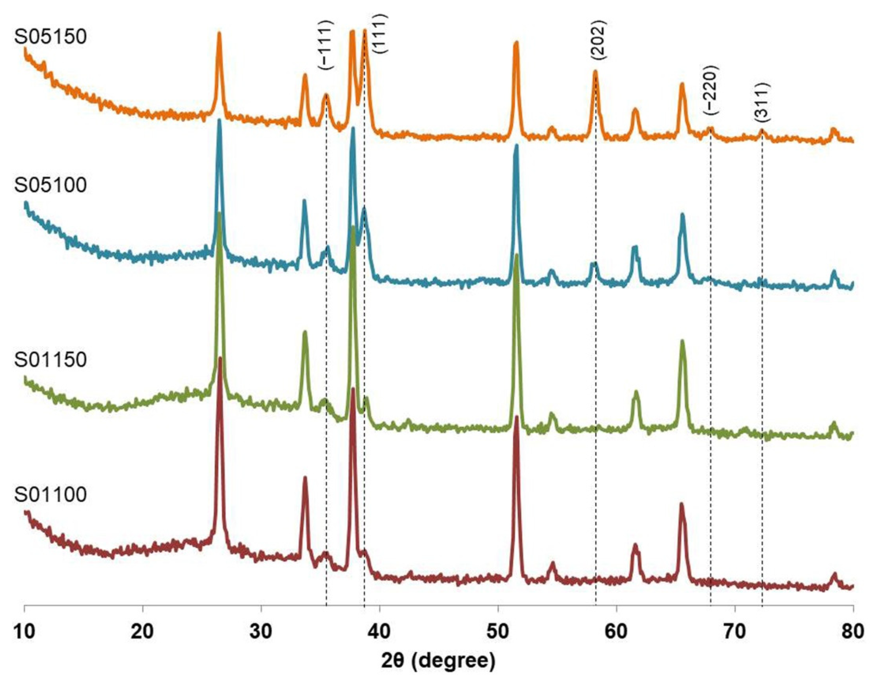
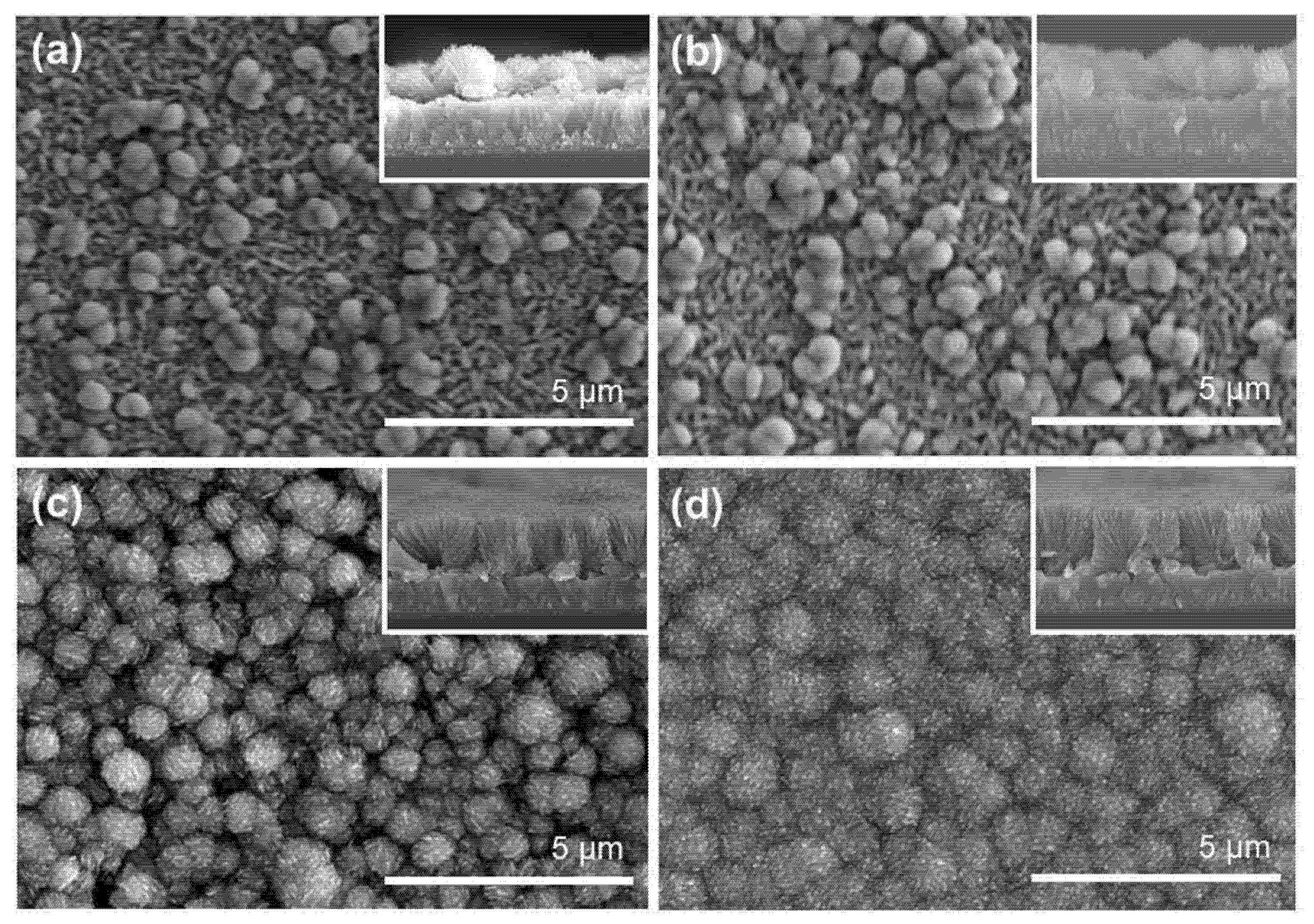
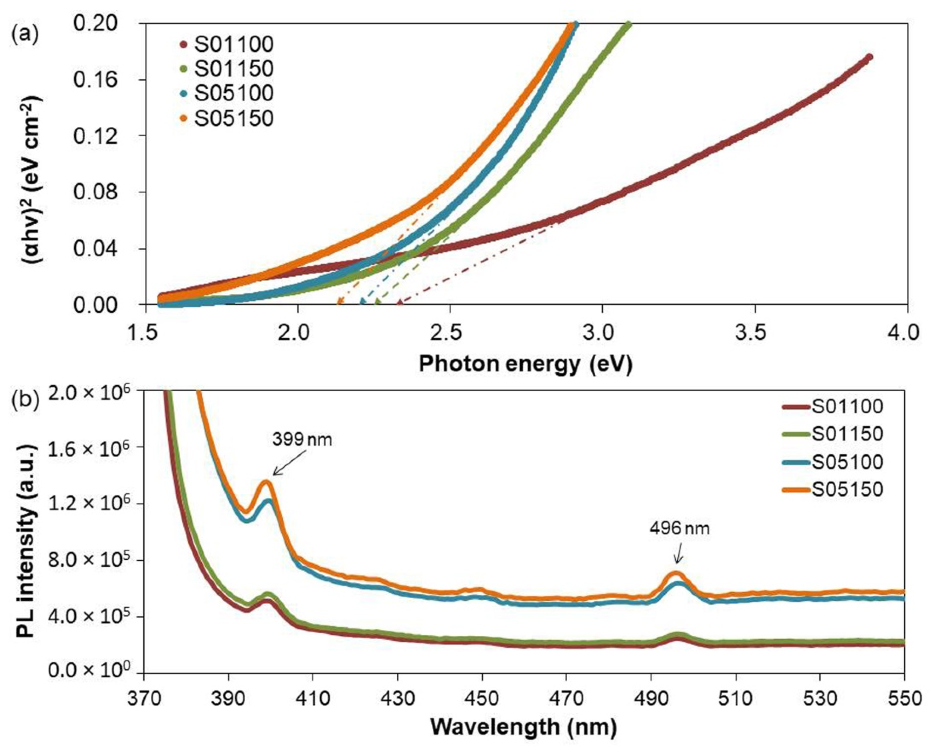
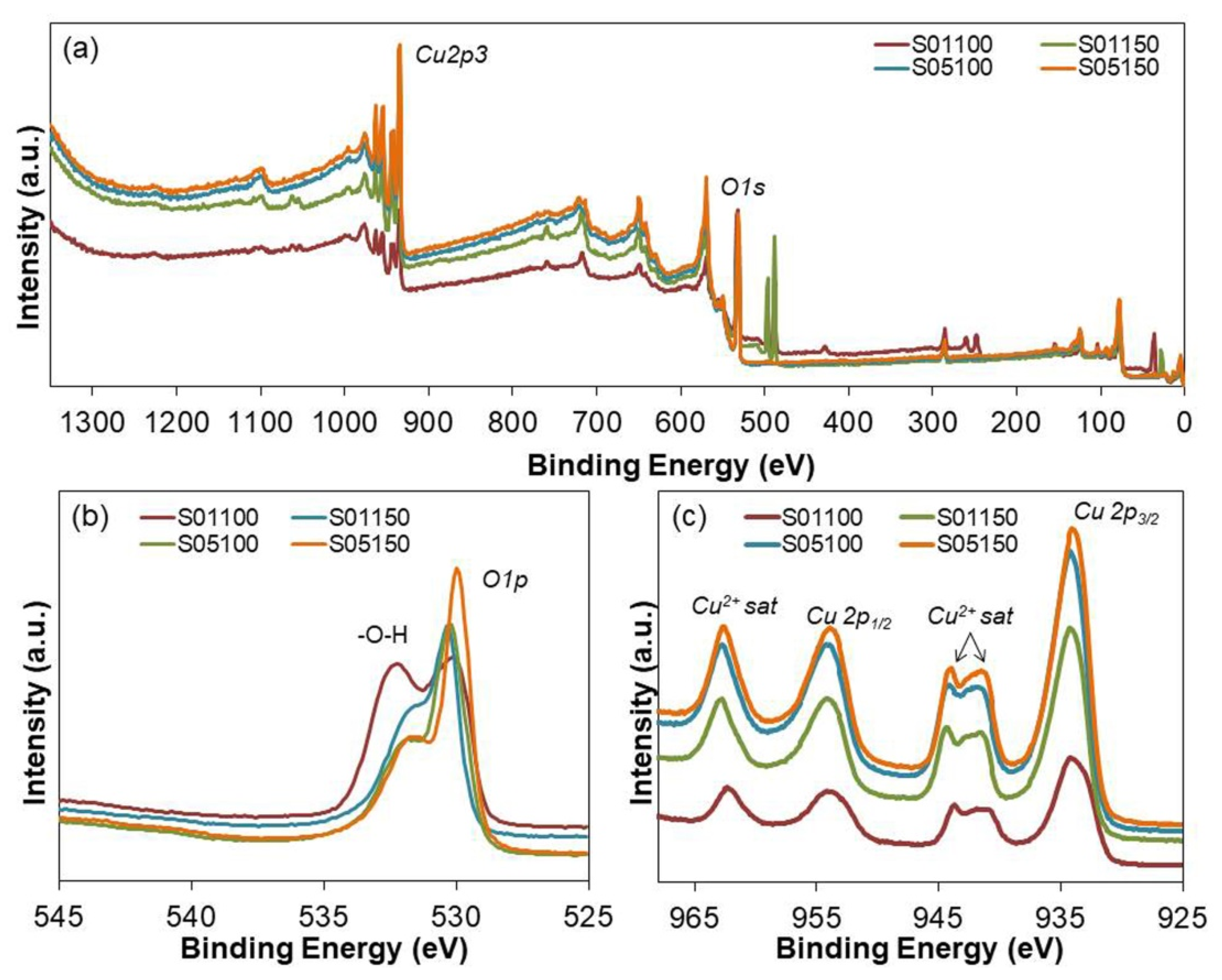
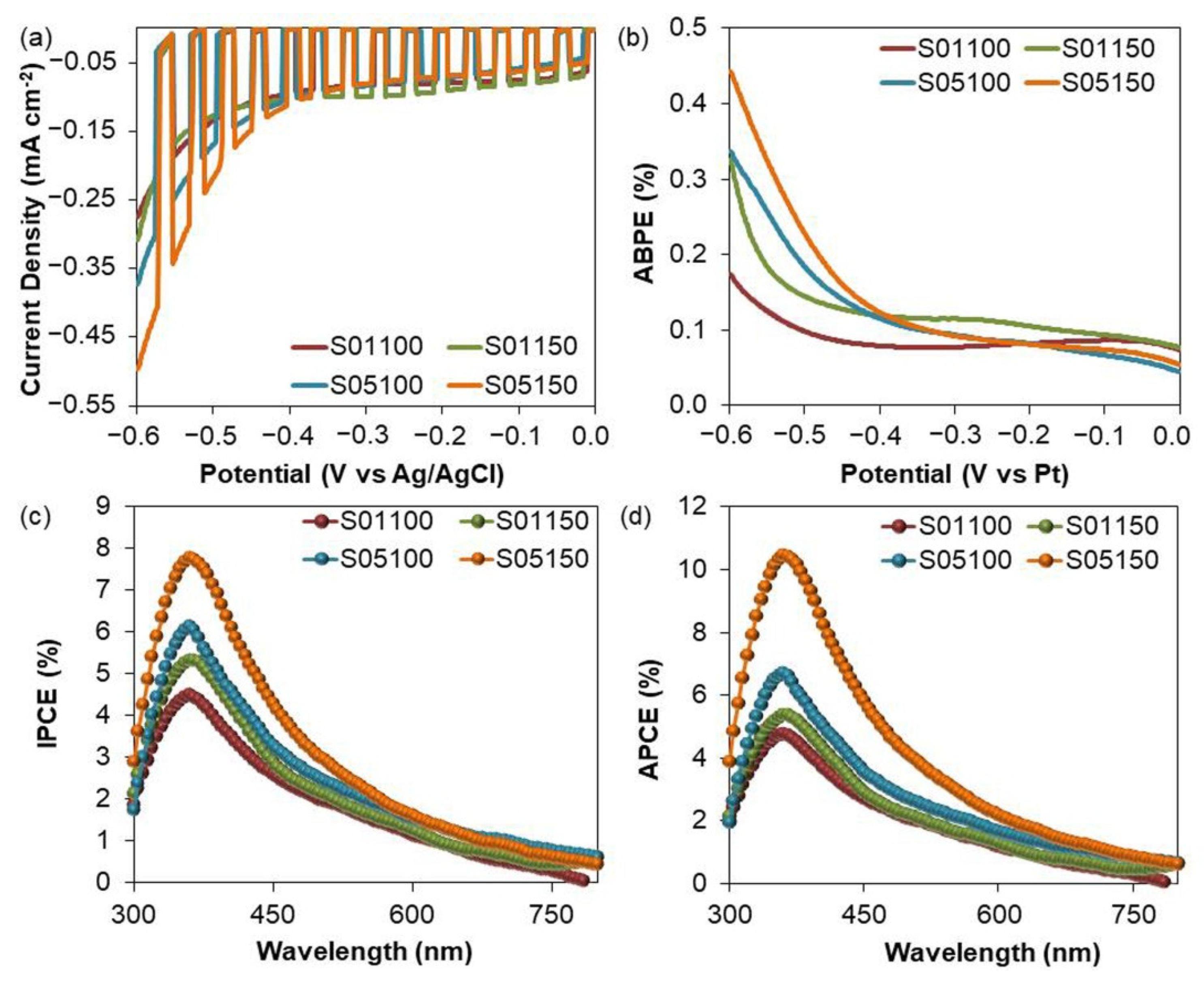
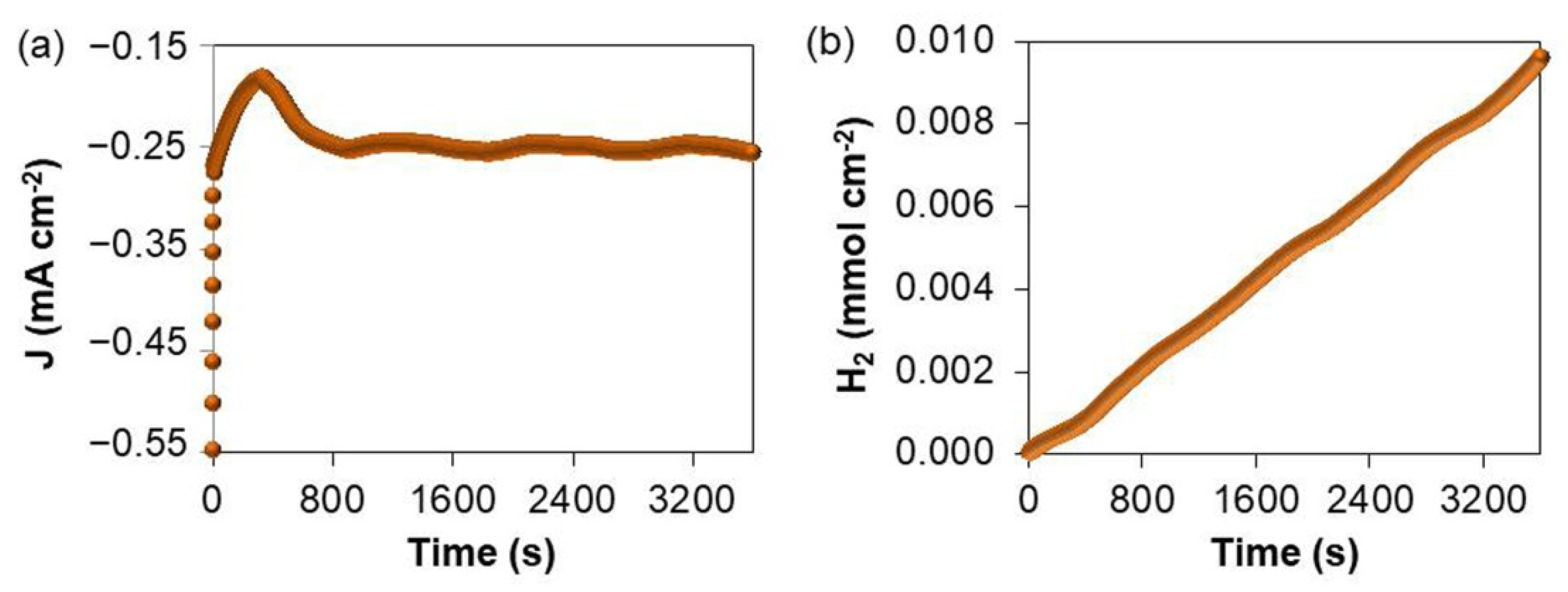
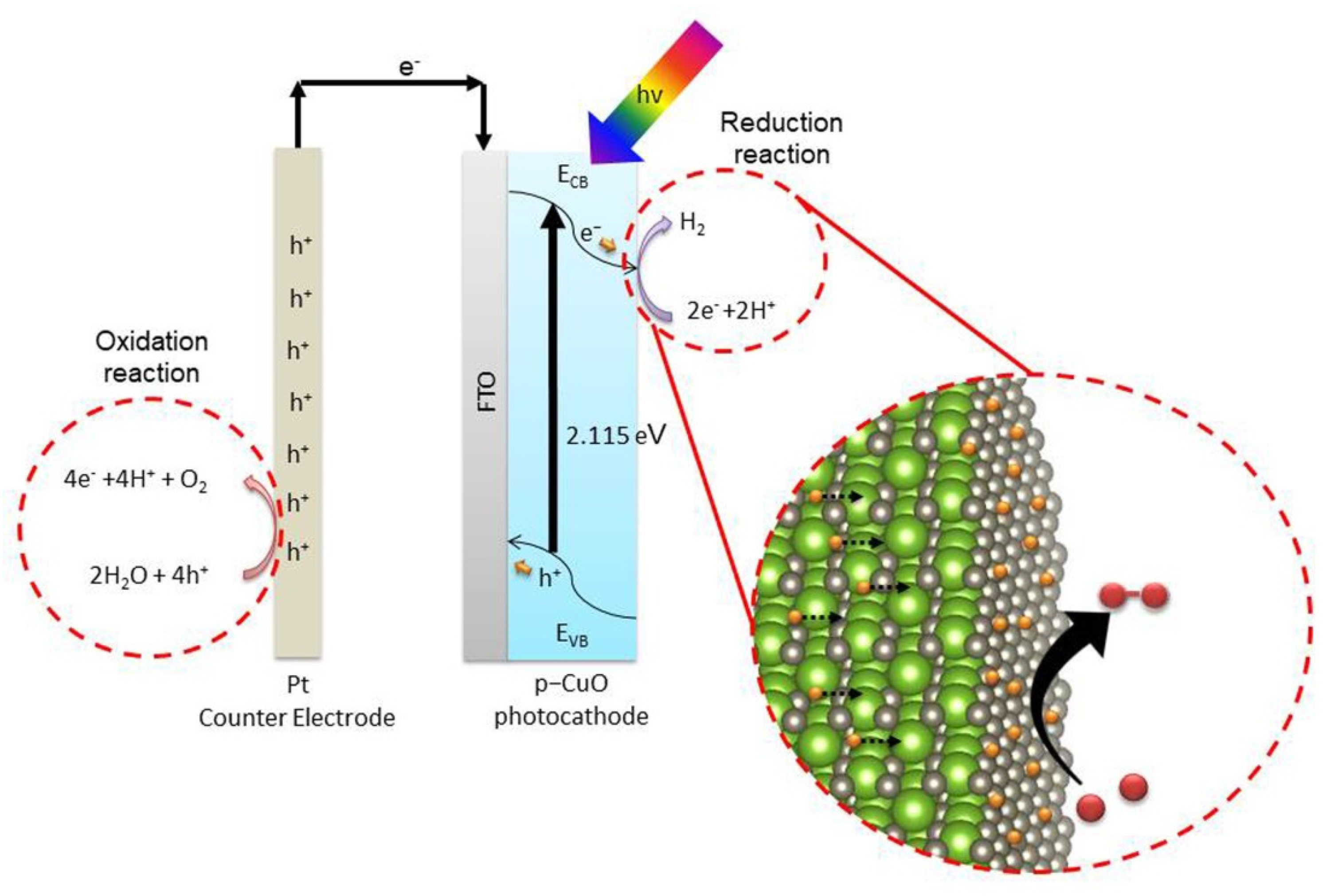
3. Results and Discussion

Under the changes in the Cp and Tr, XRD patterns were obtained, showing the changes in the peaks and planes. Figure 1 shows that five peaks were observed at 2θ~35.478°, 38.780°, 58.198°, 67.878°, and 72.33° for five planes (−1 1 1), (1 1 1), (2 0 2), (−2 2 0), and (3 1 1), respectively, compared to ICDD No#00-041-0254, and unmarked peaks represent the peaks of FTO. Increases in the Cp and Tr resulted in an increase in the peak intensity, significantly at the peaks (−1 1 1) and (1 1 1) in all samples. This indicates the high crystallinity of the samples [20,22]. From the XRD samples in Figure 1, only the S05150 sample has all five peaks of CuO, while some peaks are absent in the others. Particularly, there are no peaks for the (2 0 2), (−2 2 0), and (3 1 1) planes at the low Cp. Furthermore, there is no peak position of the Cu2O or Cu(OH)2 phase. These results reveal that the S05150 sample had good crystallinity, and the purity of the CuO in the prepared sample can be confirmed with certainty.
Table 1 reveals the crystallographic parameters of these samples. The average crystallite size increased as the Cp and Tr increased. Since the rate of the reaction increased faster at higher temperatures, the crystals grew to larger sizes [25]. The determined dislocation density and microstrain varied inversely with the crystallite size; the reason for this is that an elevation in the temperature increases the crystalline size of the film, leading to the appearance of reduced grain boundaries [25]. The lattice parameters of samples changed from 4.1960 to 4.2949 Å. The variations in the lattice parameters of the prepared CuO thin films compared with the bulk values demonstrate the presence of strain in the film.
The size and shape distribution as well as the agglomeration of the prepared materials were often influenced by the Tr of the synthesis. Figure 2 shows the top view and cross-section SEM images of the prepared CuO thin films at different temperatures. It can be easily observed that the CuO thin film consisted of spherical particles that grew close together, without any cracks or voids. These SEM images show the changes in the morphology, with larger crystallite sizes with an increasing reaction temperature. This result agrees with the crystallite size values obtained from the XRD database (Table 1). Both the Tr and Cp also affected the sizes and shapes of the particles. At lower temperatures, the crystal particles were smaller and/or some uneven carcasses, as tall and convex growths, appeared (in the case of S05100). Both S01100 and S01150 had non-smooth films even when synthesized at higher (150 °C) or lower temperatures (100 °C), which can be explained by having a low Cp. There were not enough Cu2+ ions to grow crystals, and thus, the nanoparticles and thin films consisted of small nanoparticles and were unevenly distributed on the surface of the substrate. In contrast, at higher temperatures and higher precursor concentrations, the particles grew rapidly, creating an even film on the surface of the substrate (S05150). The increases in the crystal size values were accompanied by an increase in the film thickness due to a high Cp and Tr. These inset cross-section images also indicate that the S05150 sample had an even film and low roughness; the thickness of this film was about ~920 nm. Based on this, the growth rate of copper oxide nanocrystals was calculated as 1.28 nm per min. Increasing the thickness of the CuO film supported the thin film’s ability to absorb light, which helped to enhance the optical current density. Too much thickness, however, led to increased resistance, which resulted in lower optical current density [2,26]. This result shows that good crystalline parameters of the broccoli-like structured CuO thin films were obtained at 150 °C with 0.5 M precursor solution.
Figure 3a shows the graph of the optical bandgaps for all samples, and the values are given in Table 1. The calculated bandgap values of CuO thin films decreased with increasing Tr values, especially when increasing the Tr and Cp, and the bandgap values decreased from 2.295 eV to 2.115 eV. The change in crystallinity and the number of defects in the structure at a high Tr led to the change in the bandgap values. Additionally, the bandgap values of CuO thin films synthesized at a low Cp were also higher than at a high Cp. This result occurred due to the poor growth of CuO crystals on the FTO substrate, which is demonstrated in Figure 2.
The observed results show that the Tr and Cp factors during the material synthesis were very important for the change in the bandgap. This result is in good agreement with the previous reports [20,21,25,27,28]. The photoluminescence spectra of CuO thin films are given in Figure 3b. There are two emission peaks in these spectra, at 399 nm (purple) and 496 nm (green), which are approximately close together with a very small red shift. The purple emission peak (3.1 eV) corresponds to the band edge emission [29]. The green peaks (2.5 eV) of CuO indicate the transition electron progression near the conduction band and the single ionized oxygen vacancy because, in the valence band, a single ionized electron combines with the holes [30,31].
The XPS technique was used to analyze the valence state of CuO thin films. The XPS diffraction peaks of the CuO thin films were not significantly different in terms of the shapes and positions of the peaks. However, the intensity of each sample was significantly different. The investigated XPS spectrum (Figure 4a) clearly indicates the presence of O and Cu elements in the scanned samples in the binding energy range of 0 to 1400 eV. Figure 4b shows the high-resolution XPS spectrum of the O 1s region, with the main peaks at 529.9–530.4 eV described for the presence of O atoms in the Cu–O bonds in the samples. Furthermore, the peaks between 531.0 and 532.3 eV indicate the presence of O atoms in the –OH group on the CuO surface [3,32]. In particular, the peak of the –OH bonds of sample S01100 is higher than that of other samples, which may indicate that H2O is physically or chemically absorbed on or within the sample surface [33,34]. This result is well-matched with previous reports [19]. The high-resolution XPS spectrum of Cu 2p was given in Figure 4c, These two peaks at 934.1 eV and 953.9 eV represent the Cu 2p3/2 and Cu 2p1/2, which represent the characteristic of Cu (II) in CuO. Three satellite peaks with binding energies of 941.2 eV, 944.3 eV, and 962.2 eV confirm the existence of CuO in the composites [34,35]. Furthermore, the intensity of the XPS peaks in Figure 4a–c represents the change in the precursor concentration. The precursor concentration and the peak intensity are proportional to each other, which is significant for the experiment. Additionally, the shifts in the XPS peaks represent the changes in the charge density in the atoms due to the changes in the synthesis environmental conditions. An increase in temperature and/or an increase in the precursor concentration results in a change in the binding energy around the atom, representing the oxidation state of that reaction [36].
To evaluate the potential of the prepared CuO thin films as the photocathodes in the water splitting application, a three-electrode configuration was established as described above. Figure 5a provides the chopped current density performance of four samples with a potential range of −0.6 V to 0 V (vs. Ag/AgCl) with an alternating light on/off interval of 2 s in the 0.5 M Na2SO4 electrolyte (pH 6.8). The photocurrent density values were completely different at different reaction temperatures. For the CuO photocathodes, the photocurrent density increased when the potential was more negative; a similar phenomenon has been observed in previous reports [2,37].
The photocurrent density reached 0.5 mA/cm2 at −0.6 V vs. Ag/AgCl for CuO thin films synthesized at 150 °C with a 0.5 M precursor solution, which is 1.8 times higher than the least efficient sample, which was the S01100 sample. Furthermore, the enhanced current density for negative potential (cathode direction from -0.6 V to 0 V relative to Ag/AgCl) suggests that these CuO samples are p-type for transporting the majority of carriers. The samples synthesized at a low Cp have a low current density and vice versa. Moreover, as-prepared samples with a higher Tr exhibited a higher photocurrent density. The S05150 sample’s lower bandgap, higher crystal size, suitable thickness, and uniform surface morphology help to produce higher optical current densities than other types [17,38,39], as evidenced by the structural measurements discussed above. As shown in Figure 5b, the applied potential at −0.6 V gave the maximum solar conversion efficiency (ABPE) (sample S05150 reached 0.45%). This efficiency increase is probably due to the efficient charge transfer on the interface of photocathodes and electrolytes and the suppression of electron–hole recombination [16].
IPCE, as an external quantum yield, was used as a function of the illumination wavelength to calculate the received light flux per incident photon flux. Meanwhile, APCE was used to depict the photocurrent obtained per incident photon absorbed [20]. The APCE, known as internal quantum efficiency, was obtained from the division of ICPE and the absorbance at the same wavelength. Both measurements are very useful for describing the photocurrent density as a function of the wavelength [24]. Figure 5c,d plot the IPCE and APCE, respectively. The IPCE and APCE values of all CuO thin films decreased rapidly from wavelengths greater than 400 nm and ends near 800 nm. As expected, the overall conversion efficiency of the S05150 sample was the highest, at 7.78% and 10.46% for IPCE and APCE, respectively. The S05150 sample was able to absorb to ~600 nm (based on the optical bandgap); the ICPE and APCE plots, however, show that most of the optical current densities in the photoelectrodes were only observed at 330–400 nm, that is, the violet part of the light spectrum had a good transition, and the incident light with a longer wavelength did not contribute to the photocurrent. This result shows that the photo-generated electrons had relatively short diffusion lengths. Thus, optimizing CuO synthesis will improve the carrier collection to reduce the acceptor density by expanding the charge region [39]. To investigate the photo corrosion stability of the CuO photocathode, the operating time under constant light at a constant applied voltage (−0.6 V) of the S05150 sample was measured. The long-term photocurrent measurement in Figure 6a clearly shows the high photo corrosion stability of the photocathode within 3600 s. Quantitatively, it is possible to calculate the number of moles of produced hydrogen by using Faraday’s law of electrolysis as a function of time (Equation (8)).
H 2 ( moles ) = 0 t J dt F
where J is the current density (mA/cm2) measured under a constant applied potential (−0.6 V), t is the measured time (second), and F is the Faraday constant (96.500 C/mol) [16]. The number of produced hydrogen (moles) is shown in the plots of J and t in Figure 6b. The S05150 CuO photocathode is stable and cost-effective for practical hydrogen production. Although the efficiency of the S05150 sample was rather low compared to previous reports, the results are still much more striking and comparable to other treatments in this study. Table 2 shows the comparison of the photocurrent density of the S05150 sample with other materials. Compared to the results of other studies, although the sample S05150 had a lower performance than the other samples, it had a shorter synthesis time, lower temperature, and no templates or other supporting elements.
The mechanism of the photochemical reaction of the CuO thin films was given in Figure 7. The photoelectrochemical reactivity of CuO thin film materials under the illumination of light generates electrons and holes [19]. When the negative potential is applied to the electrode, the bending band at the electrode/electrolyte interface is directed downwards, and the photo-generated electrons move to the electrode’s surface and reduce water to hydrogen (the reduction reaction) [19,43]. In addition, the photo-generated holes move to the Pt counter electrode from the photocathode through the external circuit and participate in the oxidation reaction of water to produce oxygen (oxidation reaction) [19,43].

4. Conclusions

This work contributes the basis for the development of stable and low-cost fabrication CuO photocathodes for photoelectrochemical water splitting applications. Broccoli-like structured CuO thin film has been synthesized successfully using the facile hydrothermal method. The effects of the Cp and Tr on the morphological, structural, and optical properties of CuO thin films have been discussed. Both XRD and SEM analyses have shown that a synthesis temperature of 150 °C and a 0.5 M precursor concentration are suitable for growing pure broccoli-like CuO nanostructures with good crystallinity. The oxidation state of Cu determined from the XPS spectrum was +2, so it can be confirmed that pure CuO was formed. The defined bandgap values decreased with increasing Cp and Tr, and the optical transition was assumed to be a direct transition. The IPCE and APCE values of the S01150 photocathodes reached 7.78% and 10.46%, respectively, at the purple part of the light spectrum, which is 2 times higher than that of pure S01100 photocathodes. The S05150 sample exhibited a better water-splitting ability as compared to the other samples, with a measured photocurrent density of 0.5 mA/cm2 at −0.6 V vs. Ag/AgCl. Moreover, the stability measurement indicated the S05150 photocathode is stable and can serve as a highly potential photocathode for hydrogen production.

Author Contributions

Writing—original draft preparation, conceptualization, data interpretation, N.H.L. and N.T.N.T.; data curation validation, resource, C.T.T.T.; visualization, formal analysis, J.J.; writing—review and editing, A.M.T., M.S.T. and K.-s.A.; supervision, J.H.J.; project administration, funding acquisition, C.-D.K. All authors have read and agreed to the published version of the manuscript.

Funding

This research was supported by the Basic Science Research Program through the National Research Foundation of Korea (NRF), funded by the Ministry of Education (No. NRF-2019R1I1A1A01061738).

Institutional Review Board Statement

Not applicable.

Informed Consent Statement

Not applicable.

Data Availability Statement

Not applicable.

Conflicts of Interest

The authors declare no conflict of interest.

References

  1. Tuller, H.L. Solar to fuels conversion technologies: A perspective. Mater. Renew. Sustain. Energy 2017, 6, 3. [Google Scholar] [CrossRef] [PubMed] [Green Version]
  2. Guo, X.; Diao, P.; Xu, D.; Huang, S.; Yang, Y.; Jin, T.; Wu, Q.; Xiang, M.; Zhang, M. CuO/Pd composite photocathodes for photoelectrochemical hydrogen evolution reaction. Int. J. Hydrogen Energy 2014, 39, 7686–7696. [Google Scholar] [CrossRef]
  3. Liu, X.; Zheng, H.; Sun, Z.; Han, A.; Du, P. Earth-abundant copper-based bifunctional electrocatalyst for both catalytic hydrogen production and water oxidation. ACS Catal. 2015, 5, 1530–1538. [Google Scholar] [CrossRef]
  4. Zhong, Y.; Lu, Y.; Pan, Z.; Yang, J.; Du, G.; Chen, J.; Zhang, Q.; Zhou, H.; Wang, J.; Wang, C.; et al. Efficient Water Splitting System Enabled by Multifunctional Platinum-Free Electrocatalysts. Adv. Funct. Mater. 2021, 31, 2009853. [Google Scholar] [CrossRef]
  5. Chen, Z.; Duan, X.; Wei, W.; Wang, S.; Ni, B.J. Iridium-based nanomaterials for electrochemical water splitting. Nano Energy 2020, 78, 105270. [Google Scholar] [CrossRef]
  6. Yu, J.; He, Q.; Yang, G.; Zhou, W.; Shao, Z.; Ni, M. Recent advances and prospective in ruthenium-based materials for electrochemical water splitting. ACS Catal. 2019, 9, 9973–10011. [Google Scholar] [CrossRef]
  7. Zhao, J.; Gill, T.M.; Zheng, X. Enabling silicon photoanodes for efficient solar water splitting by electroless-deposited nickel. Nano Res. 2018, 11, 3499–3508. [Google Scholar] [CrossRef]
  8. Zhang, H.; Park, S.O.; Joo, S.H.; Kim, J.H.; Kwak, S.K.; Lee, J.S. Precisely-controlled, a few layers of iron titanate inverse opal structure for enhanced photoelectrochemical water splitting. Nano Energy 2019, 62, 20–29. [Google Scholar] [CrossRef]
  9. Liu, Z.; Lu, X. Multifarious function layers photoanode based on g-C3N4 for photoelectrochemical water splitting. Chin. J. Catal. 2018, 39, 1527–1533. [Google Scholar] [CrossRef]
  10. Zhu, Z.; Wan, S.; Zhao, Y.; Gu, Y.; Wang, Y.; Qin, Y.; Bu, Y. Recent advances in bismuth-based multimetal oxide photocatalysts for hydrogen production from water splitting: Competitiveness, challenges, and future perspectives. Mater. Rep. Energy 2021, 1, 100019. [Google Scholar] [CrossRef]
  11. Yoo, I.H.; Lee, Y.J.; Kalanur, S.S.; Seo, H. Assembly of nonstoichiometric molybdenum oxide on Si as pn junction photocathode for enhanced hydrogen evolution. Appl. Catal. 2020, 264, 118542. [Google Scholar] [CrossRef]
  12. Murakami, T.; Ikezoi, K.; Nagai, K.; Kato, H.; Abe, T. A Water-Splitting System with a Cobalt (II, III) Oxide Co-Catalyst-Loaded Bismuth Vanadate Photoanode Along with an Organo-Photocathode. ChemElectroChem 2020, 7, 5029–5035. [Google Scholar] [CrossRef]
  13. Han, X.; Liu, P.; Ran, R.; Wang, W.; Zhou, W.; Shao, Z. Non-metal fluorine doping in Ruddlesden–Popper perovskite oxide enables high-efficiency photocatalytic water splitting for hydrogen production. Mater. Today Energy 2022, 23, 100896. [Google Scholar] [CrossRef]
  14. Xiao, H.; Liu, P.; Wang, W.; Ran, R.; Zhou, W.; Shao, Z. Enhancing the photocatalytic activity of Ruddlesden-Popper Sr2TiO4 for hydrogen evolution through synergistic silver doping and moderate reducing pretreatment. Mater. Today Energy 2022, 23, 100899. [Google Scholar] [CrossRef]
  15. Wang, W.; Xu, M.; Xu, X.; Zhou, W.; Shao, Z. Perovskite oxide-based electrodes for high-performance photoelectrochemical water splitting. Angew. Chem. Int. Ed. 2020, 59, 136–152. [Google Scholar] [CrossRef] [PubMed]
  16. Ahmed, A.M.; Abdalla, E.M.; Shaban, M. Simple and low-cost synthesis of Ba-doped CuO thin films for highly efficient solar generation of hydrogen. J. Phys. Chem. C 2020, 124, 22347–22356. [Google Scholar] [CrossRef]
  17. Patel, M.; Pati, R.; Marathey, P.; Kim, J.; Mukhopadhyay, I.; Ray, A. Highly photoactive and photo-stable spray pyrolyzed tenorite CuO thin films for photoelectrochemical energy conversion. J. Electrochem. Soc. 2016, 163, H1195. [Google Scholar] [CrossRef]
  18. Zhou, Q.; Li, T.T.; Xu, W.; Zhu, H.L.; Zheng, Y.Q. Ultrathin nanosheets-assembled CuO flowers for highly efficient electrocatalytic water oxidation. J. Mater. Sci. 2018, 53, 8141–8150. [Google Scholar] [CrossRef]
  19. Xie, T.; Zheng, T.; Wang, R.; Bu, Y.; Ao, J.P. Fabrication of CuOx thin-film photocathodes by magnetron reactive sputtering for photoelectrochemical water reduction. Green Energy Environ. 2018, 3, 239–246. [Google Scholar] [CrossRef]
  20. Oh, H.; Ryu, H.; Lee, W.J. Effects of copper precursor concentration on the growth of cupric oxide nanorods for photoelectrode using a modified chemical bath deposition method. J. Alloys Compd. 2015, 620, 55–59. [Google Scholar] [CrossRef]
  21. Ansari, A.R.; Hammad, A.H.; Abdel-wahab, M.S.; Shariq, M.; Imran, M. Structural, optical and photoluminescence investigations of nanocrystalline CuO thin films at different microwave powers. Opt. Quantum Electron. 2020, 52, 1–16. [Google Scholar] [CrossRef]
  22. Vinothkumar, P.; Manoharan, C.; Shanmugapriya, B.; Bououdina, M. Effect of reaction time on structural, morphological, optical and photocatalytic properties of copper oxide (CuO) nanostructures. J. Mater. Sci. Mater. 2019, 30, 6249–6262. [Google Scholar] [CrossRef]
  23. Le, N.; Truong, N.T.N.; Lam, N.H.; Tamboli, A.M.; Patil, S.S.; Tamboli, M.S.; Lee, K.; Kim, E.S.; Jung, J.H. Enhanced light absorption and charge separation of In-doped ZnO nanorod arrays for photoelectrochemical water-splitting application. Int. J. Energy Res. 2021, 1–13. [Google Scholar] [CrossRef]
  24. Chen, Z.; Dinh, H.N.; Miller, E. Photoelectrochemical Water Splitting: Standards, Experimental Methods, and Protocols, 1st ed.; Springer: New York, NY, USA, 2013. [Google Scholar]
  25. Begum, A.; Hussain, A.; Rahman, A. Effect of deposition temperature on the structural and optical properties of chemically prepared nanocrystalline lead selenide thin films. Beilstein J. Nanotechnol. 2012, 3, 438–443. [Google Scholar] [CrossRef]
  26. Giraldi, T.R.; Escote, M.T.; Bernardi, M.I.B.; Bouquet, V.; Leite, E.R.; Longo, E.; Varela, J.A. Effect of Thickness on the Electrical and Optical Properties of Sb Doped SnO2 (ATO) Thin Films. J. Electroceram. 2004, 13, 159–165. [Google Scholar] [CrossRef]
  27. Xu, L.; Zheng, G.; Pei, S.; Wang, J. Investigation of optical bandgap variation and photoluminescence behavior in nanocrystalline CuO thin films. Optik 2018, 158, 382–390. [Google Scholar] [CrossRef]
  28. Moumen, A.; Hartiti, B.; Comini, E.; El Khalidi, Z.; Arachchige, H.M.M.M.; Fadili, S.; Thevenin, P. Preparation and characterization of nanostructured CuO thin films using spray pyrolysis technique. Superlattices Microstruct. 2018, 127, 2–10. [Google Scholar] [CrossRef]
  29. Sandupatla, R.R.; Veerasomaiah, P. Synthesis, characterization and photoluminescence study of CuO nanoparticles using aqueous solution method. Int. J. Nanomater. Biostruct. 2016, 6, 30–33. [Google Scholar]
  30. Lanje, A.S.; Sharma, S.J.; Pode, R.B.; Ningthoujam, R.S. Synthesis and optical characterization of copper oxide nanoparticles. Adv. Appl. Sci. Res. 2010, 1, 36–40. [Google Scholar]
  31. Gobbiner, C.R.; Dillip, G.R.; Joo, S.W.; Kekuda, D. Heterogeneity of photoluminescence properties and electronic transitions in copper oxide thin films: A thickness dependent structural and optical study. Ceram. Int. 2018, 44, 16984–16991. [Google Scholar] [CrossRef]
  32. Guerrero-Araque, D.; Acevedo-Pena, P.; Ramırez-Ortega, D.; Lartundo-Rojas, L.; Gomez, R. SnO2–TiO2 structures and the effect of CuO, CoO metal oxide on photocatalytic hydrogen production. J. Chem. Technol. Biotechnol. 2017, 92, 1531–1539. [Google Scholar] [CrossRef]
  33. Tomar, A.K.; Singh, G.; Sharma, R. K Fabrication of Modoped strontium cobaltite perovskite hybrid supercapacitor cell with high energy density and excellent cycling life. ChemSusChem 2018, 11, 4123–4130. [Google Scholar] [CrossRef] [PubMed]
  34. Lv, W.; Li, L.; Meng, Q.; Zhang, X. Molybdenum-doped CuO nanosheets on Ni foams with extraordinary specific capacitance for advanced hybrid supercapacitors. J. Mater. Sci. 2019, 55, 2492–2502. [Google Scholar] [CrossRef]
  35. Liu, Y.; Cao, X.Y.; Jiang, D.G.; Jia, D.D.; Liu, J.Q. Hierarchical CuO nanorod arrays in situ generated on three-dimensional copper foam via cyclic voltammetry oxidation for high-performance supercapacitors. J. Mater. Chem. A 2018, 6, 10474–10483. [Google Scholar] [CrossRef]
  36. Greczynski, G.; Hultman, L. Compromising science by ignorant instrument calibration—Need to revisit half a century of published XPS data. Angew. Chem. Int. Ed. 2020, 132, 5034–5038. [Google Scholar] [CrossRef]
  37. Chiang, C.Y.; Aroh, K.; Franson, N.; Satsangi, V.R.; Dass, S.; Ehrman, S. Copper oxide nanoparticle made by flame spray pyrolysis for photoelectrochemical water splitting–Part II. Photoelectrochemical study. Int. J. Hydrogen Energy 2011, 36, 15519–15526. [Google Scholar] [CrossRef]
  38. Cao, D.; Nasori, N.; Wang, Z.; Wen, L.; Xu, R.; Mi, Y.; Lei, Y. Facile surface treatment on Cu2O photocathodes for enhancing the photoelectrochemical response. Appl. Catal. 2016, 198, 398–403. [Google Scholar] [CrossRef]
  39. Hahn, N.T.; Holmberg, V.C.; Korgel, B.A.; Mullins, C.B. Electrochemical synthesis and characterization of p-CuBi2O4 thin film photocathodes. J. Phys. Chem. C 2012, 116, 6459–6466. [Google Scholar] [CrossRef]
  40. Lim, Y.F.; Chua, C.S.; Lee, C.J.J.; Chi, D. Sol–gel deposited Cu2O and CuO thin films for photocatalytic water splitting. Phys. Chem. Chem. Phys. 2014, 16, 25928–25934. [Google Scholar] [CrossRef]
  41. Li, J.; Jin, X.; Li, R.; Zhao, Y.; Wang, X.; Liu, X.; Jiao, H. Copper oxide nanowires for efficient photoelectrochemical water splitting. Appl. Catal. B 2019, 240, 1–8. [Google Scholar] [CrossRef]
  42. Kushwaha, A.; Moakhar, R.S.; Goh, G.K.; Dalapati, G.K. Morphologically tailored CuO photocathode using aqueous solution technique for enhanced visible light driven water splitting. J. Photochem. Photobiol. A Chem. 2017, 337, 54–61. [Google Scholar] [CrossRef]
  43. Kalanur, S.S.; Duy, L.T.; Seo, H. Recent Progress in Photoelectrochemical Water Splitting Activity of WO3 Photoanodes. Top. Catal. 2018, 61, 1043–1076. [Google Scholar] [CrossRef]
Figure 1. XRD patterns of S01100, S01150, S05100, and S05150 samples prepared on FTO substrate. The CuO thin films were synthesized by hydrothermal method at 100 °C and 150 °C for 12 h.
Metals 12 00484 g001
Figure 2. SEM images of CuO thin films synthesized under different temperatures (100 °C and 150 °C) and precursor concentration (0.1 M and 0.5 M). Note: (a) S01100; (b) S01150; (c) S05100; (d) S05150.
Metals 12 00484 g002
Figure 3. (a) The Tauc plot and (b) photoluminescence spectra of CuO thin films.
Metals 12 00484 g003
Figure 4. (a) The survey scan XPS spectra of CuO thin films; (b) the high-resolution XPS of O1s; (c) the high-resolution XPS of Cu2p.
Metals 12 00484 g004
Figure 5. (a) The photocurrent density of CuO thin-films at applied potential range from −0.6 to 0 V (vs. Ag/AgCl); (bd) the ABPE, IPCE, and APCE of CuO thin films, respectively.
Metals 12 00484 g005
Figure 6. (a) The photo corrosion stability measurement and (b) the calculated H2 production using S05150 CuO photocathodes.
Metals 12 00484 g006
Figure 7. Schematic of the mechanism of the photochemical reaction of the CuO thin films. The green dots and gray dots are Cu and O, respectively, in the crystal structure of CuO; electrons (yellow dots) are formed inside the CuO photocathode when illuminated; then, they move to the surface of the electrode and interact with the red dots (H+ ions) to form H2 bubbles.
Metals 12 00484 g007
Table 1. The crystallographic parameters of samples.
Crystallographic ParametersS01100S01150S05100S05150
Lattice parameter (Å)4.19604.20044.29494.2218
Crystallite size (nm)3.08273.08763.46603.6422
Thickness (µm)0.43030.51890.89870.9205
Microstrain (%)0.15780.14590.14490.1287
Dislocation density (δ)5.71 × 10−25.70 × 10−25.46 × 10−25.66 × 10−2
Bandgap (eV)2.29502.23402.17202.1150
Table 2. The comparison of photoelectrochemical water splitting efficiency of CuO broccoli-like structure (S05150) and other materials.
MaterialJ (mA/cm2)Synthesis MethodReference
S05150
CuO (broccoli-like structure)
0.5 mA/cm2 at −0.6 V vs. Ag/AgClHydrothermal method (Temp. = 150 °C,
Conc. = 0.5 M, Time = 12 h)
In this study
Cu2O
CuO
Cu2O-NiOx
0.28 mA/cm2
0.35 mA/cm2
0.47 mA/cm2
at 0.05 V vs. RHE
Sol-gel method (Conc. = 0.3 M, Time = 2 days) [40]
CuO
(wire-like structure)
~1.4 mA/cm2 at 0 V vs. RHEThermal treatment + electro deposition method (Template: Cu foil, Temp. = 800 °C in air, Pt cocatalyst deposited, Time = 300 s)[41]
CuO nanosheet
CuO nanoleaves
1.1 mA/cm2
1.5 mA/cm2
at 0 V vs. RHE
Dip coating (CuO nano seed preparation) + Sol-gel method (2-methoxiethanol and monoethanolamine) + Heat treatment (350 °C for 1 h)[42]
Publisher’s Note: MDPI stays neutral with regard to jurisdictional claims in published maps and institutional affiliations.

