1. Introduction
The family of two-dimensional (2D) semiconducting transition metal dichalcogenides (TMDs), such as MoS
2, WS
2, MoSe
2 and others, has grown significantly [
1]. TMDs exhibit strong absorption in the visible range and show promise for next-generation optoelectronic devices. These properties araised from tightly bound excitons with binding energies in the order of several hundred millielectronvolts [
2,
3]. These excitons appear as a consequence of quantum confinement and reduced dielectric screening, which enhances the Coulomb interactions between electrons and holes. Further enhancement of these properties can be achieved by reduction of the dimensionality by the formation of nanotubes from similar materials. Following the discovery of carbon nanotubes (CNTs), inorganic nanotubes (NT) from TMDCs were reported. These materials could be used in a number of real applications in the fields of tribology, machining, nanophotonics, and nanooptics [
4,
5].
Noble TMD NT have unique properties due to the size-dependent properties of both NT and metal nanoparticles [
6]. Being semiconducting, TMD NT decorated with gold and silver nanoparticles are of particular importance because of the tunability of their optoelectronic properties. Previously, the optical properties of WS
2NT were partially studied [
5].
In this article, the deposition of thin WS2NT by vacuum filtration and CNT by the dry transfer technique is implemented. Except for the standard characterization methods (TEM, SEM, UV-Vis-IR spectroscopy, Raman), we also present transmission measurements in the THz range (0.2 THz to 3 THz). The experimentally observed dependencies are described by establishing the relation between the size of both types of NT and the electromagnetic response. The comparison between NT made of different materials is given.
2. Methods
The samples were prepared from commercial WS
2NT, produced by NanoMaterials Ltd. in ethanol suspension. After sonication, the thin films were obtained by the vacuum filtration method using a nitrocellulose membrane. The obtained films were transferred to the z-cut quartz substrates and dissolved with acetone. The thin CNT films were obtained by the aerosol synthesis method and transferred to the same z-cut quartz substrates by using the dry transfer technique [
7].
Scanning electron microscope (SEM) imaging was performed with a high-resolution SEM Zeiss Ultra, Germany, with a secondary electron detector, an acceleration voltage of 5.0 kV, and a working distance of 6.0 mm. Transmission electron microscopy (TEM) imaging was performed using a JEOL JEM-2100, Tokyo, Japan, electron microscope.
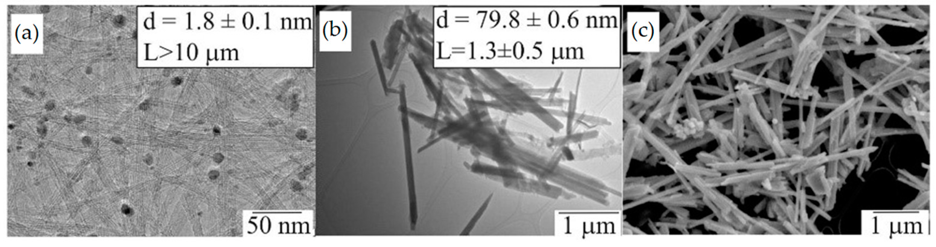
Figure 1 shows representative TEM and SEM images of the WS
2NT and CNT films. The NT dimensions are detailed in
Table 1. TEM and SEM images allow us to estimate the average diameter and length of NT, which are detailed in
Table 1.
The choice of a 1 mm-thick quartz substrate meant that the THz spectral resolution was not reduced substantially in comparison to the THz spectral resolution for the spectrometer; the same applies for the transparency in this frequency range. Equilibrium absorbance spectra were determined via homemade THz time-domain spectroscopy (0.2–3 THz range) using a Cary 5000 UV/VIS/NIR, Varian, USA, spectrophotometer (250–2500 nm). For Raman spectra, a confocal micro-spectrometer (Labram, Jobin-Yvon Horiba, Japan) with a 520 nm laser at 0.58 mW (with spectral resolution 1 cm−1 and spatial resolution 1.5 μm) was used. For chemical doping, pristine WS2NT and CNT films were drop-coated with HAuCl4 ethanol solution. After 20 s, the solvent had completely evaporated. Samples were stored in air and measured over a period of weeks.
3. Results
It is known that the optical properties of CNT and WS
2NT samples depend on the diameter. The optical absorbance of the CNT sample showed characteristic strong peaks of excitonic transitions in semiconducting (E
S11, E
S22) and metallic (E
M11) NT in the absorption spectra at wavelengths of 2300, 1240 and 870 nm, respectively. These excitonic transitions correspond to the CNTs with a diameter of 1.8 nm. For WS
2NT, the peaks at 670, 560 and 500 nm correspond to the direct A, direct B and indirect C excitonic transitions, respectively. The intensive peak at about 730 nm corresponds to Mie scattering originating from surface plasmon resonance. The comparison with the results in [
5] allows us to conclude that all the absorption peaks are red-shifted by 47 nm with respect to WS
2NT with a diameter of 36 nm. This observation is in agreement with the larger diameter of the investigated sample, proved by TEM.
A large change in absorbance occurs upon adsorption doping with HAuCl4. Because of this CNT, the chemical potential lowers, depleting the valence bands of electrons and suppressing the excitonic optical absorption transitions. An additional absorption peak arose between 1000 and 2000 nm, which can be attributed to intersubband transitions. A shift in the excitonic peaks for doped WS2NT was also observed. The mentioned electron transfer occurs due to the difference between the Fermi level of WS2NT and CNT, and the rather high reduction potential of HAuCl4.
Raman spectra showed typical radial breathing modes (RBM) of CNT with a diameter of 1.8 nm, which is also in agreement with the TEM data. WS
2NT are characterized by two peaks, corresponding to longitudinal (E
12g) and transversal (A
1g) phonon modes with wavelengths of 417 and 351 cm
−1, respectively. These modes are shifted by 1 and 5 cm
−1 in comparison to the one-layer 2D WS
2, and 2 and 4 cm
−1 in comparison to the multilayer 2D WS
2 [
7], which is explained by the NT curvature influence on oscillating lattice modes. Doping with HAuCl
4 results in a shift towards higher frequency in both CNT and WS
2, which indicates p-doping.
Finally, the real and imaginary parts of the equilibrium sheet terahertz conductivity of CNT and WS
2NT films were obtained. The increase in the real part of the CNT conductivity towards lower frequencies is caused by the contributions of the free charge absorption, described by the Drude model, and axial plasmons, described by the Lorentz model [
8]. The conductivity of WS
2NT, on the contrary, increases towards higher frequencies, which evidences the presence of axial plasmons with a resonant frequency in the far or middle infrared region. Doping leads to broadening of the real part of the conductivity of the CNT, with a simultaneous increase in the amplitude. Meanwhile, in WS
2NT, a shift in the conductivity towards higher frequency was observed due to the same reason.
4. Conclusions
The structure and optoelectronic properties of doped and pristine CNT and WS2NT were examined by numerous techniques, such as absorption, Raman, and THz time-domain spectroscopy. Overall, WS2NT possesses optoelectronic properties that change because of the curvature, quantum confinement, and localization in comparison to their 2D counterparts. Doping with HAuCl4 results in the tunability of all optoelectronic properties.
Author Contributions
Conceptualization, M.G.B. and M.I.P.; formal analysis, A.E.G. and M.I.P.; investigation, M.I.P., G.A.K., S.N., A.V.S., D.I.Y., A.E.G. and A.G.N.; resources, A.Z., R.T.; writing—original draft preparation, M.G.B. and M.I.P.; visualization, M.I.P.; supervision, M.G.B.; project administration, M.G.B., A.V.A.; funding acquisition, M.G.B., V.V. All authors have read and agreed to the published version of the manuscript.
Funding
Authors acknowledge the Russian Science Foundation project No. 21-79-10097, Ministry of Science and Higher Education of the Russian Federation project No. 075-15-2021-606, and Russian Foundation for Basic Research No. 18-29-27010 MK.
Institutional Review Board Statement
Not applicable.
Informed Consent Statement
Not applicable.
Data Availability Statement
Not applicable.
Conflicts of Interest
The authors declare no conflict of interest.
References
- Manzeli, S.; Ovchinnikov, D.; Pasquier, D.; Yazyev, O.V.; Kis, A. 2D transition metal dichalcogenides. Nat. Rev. Mater. 2017, 2, 17033. [Google Scholar] [CrossRef]
- Wang, G.; Chernikov, A.; Glazov, M.M.; Heinz, T.F.; Marie, X.; Amand, T.; Urbaszek, B. Colloquium: Excitons in Atomically Thin Transition Metal Dichalcogenides. Rev. Mod. Phys. 2018, 90, 021001. [Google Scholar] [CrossRef]
- Chernikov, A.; Berkelbach, T.C.; Hill, H.M.; Rigosi, A.; Li, Y.L.; Aslan, O.B.; Reichman, D.R.; Hybertsen, M.S.; Heinz, T.F. Exciton Binding Energy and Nonhydrogenic Rydberg Series in Monolayer WS2. Phys. Rev. Lett. 2014, 113, 076802. [Google Scholar] [CrossRef]
- Guo, J.; Xiang, R.; Cheng, T.; Maruyama, S.; Li, Y. One-Dimensional van der Waals Heterostructures: A Perspective. ACS Nanosci. 2022, 2, 3–11. [Google Scholar] [CrossRef]
- Sinha, S.S.; Yadgarov, L.; Aliev, S.B.; Feldman, Y.; Pinkas, I.; Chithaiah, P.; Ghosh, S.; Idelevich, A.; Zak, A.; Tenne, R. MoS2 and WS2 Nanotubes: Synthesis, Structural Elucidation, and Optical Characterization. J. Phys. Chem. C 2021, 125, 6324–6340. [Google Scholar]
- Polyakov, A.Y.; Yadgarov, L.; Popovitz-Biro, R.; Lebedev, V.A.; Pinkas, I.; Rosentsveig, R.; Feldman, Y.; Goldt, A.E.; Goodilin, E.A.; Tenne, R. Decoration of WS2 Nanotubes and Fullerene-Like MoS2 with Gold Nanoparticles. J. Phys. Chem. C 2014, 118, 2161–2169. [Google Scholar] [CrossRef]
- Nasibulin, A.G.; Moisala, A.; Brown, D.P.; Jiang, H.; Kauppinen, E.I. A Novel Aerosol Method for Single Walled Carbon Nanotube Synthesis. Chem. Phys. Lett. 2005, 402, 227–232. [Google Scholar] [CrossRef]
- Burdanova, M.G.; Tsapenko, A.P.; Kharlamova, M.V.; Kauppinen, E.I.; Gorshunov, B.P.; Kono, J.; Lloyd-Hughes, J. A Review of the Terahertz Conductivity and Photoconductivity of Carbon Nanotubes and Heteronanotubes. Adv. Opt. Mater. 2021, 9, 2101042. [Google Scholar] [CrossRef]
| Publisher’s Note: MDPI stays neutral with regard to jurisdictional claims in published maps and institutional affiliations. |
© 2022 by the authors. Licensee MDPI, Basel, Switzerland. This article is an open access article distributed under the terms and conditions of the Creative Commons Attribution (CC BY) license (https://creativecommons.org/licenses/by/4.0/).

 ,
, 

