
The Effect of the Solution Flow and Electrical Field on the Homogeneity of Large-Scale Electrodeposited ZnO Nanorods

 ,
,
Abstract
:1. Introduction
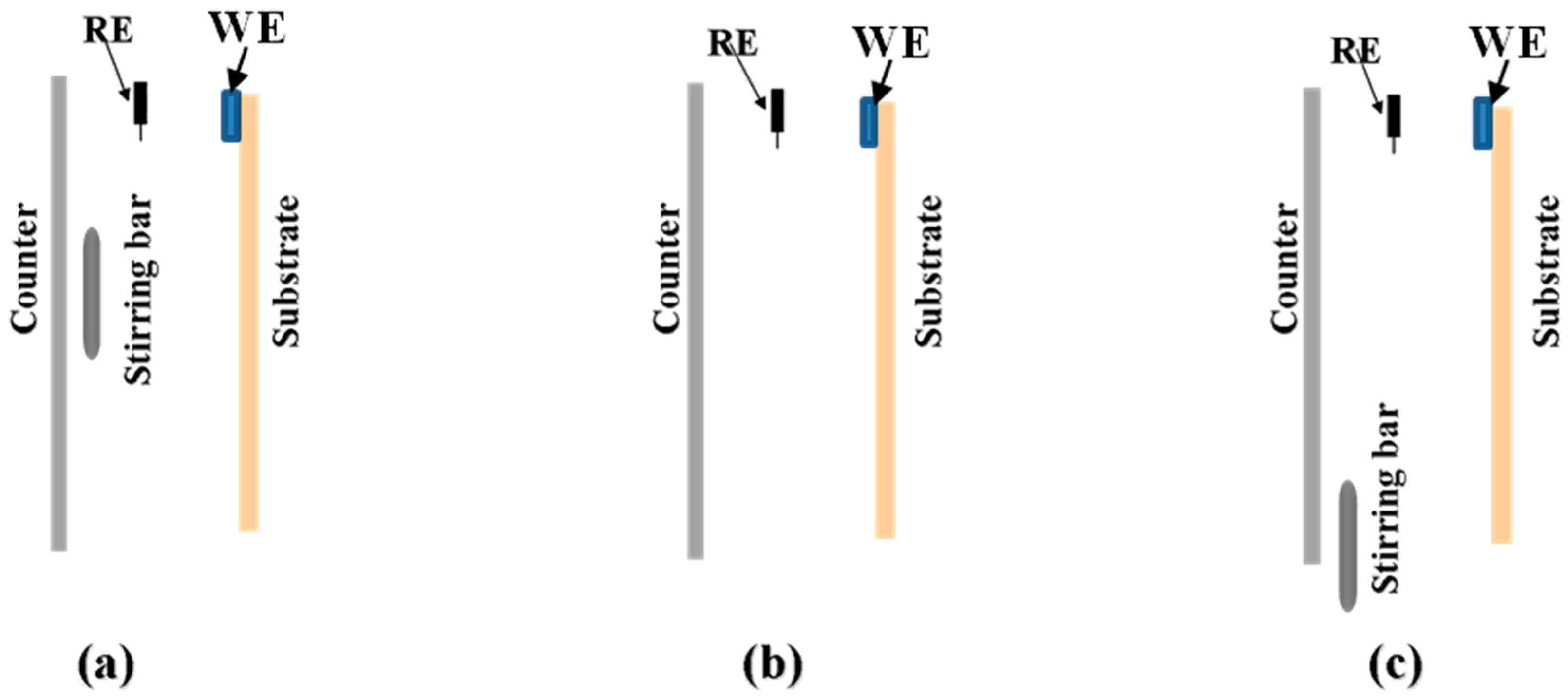
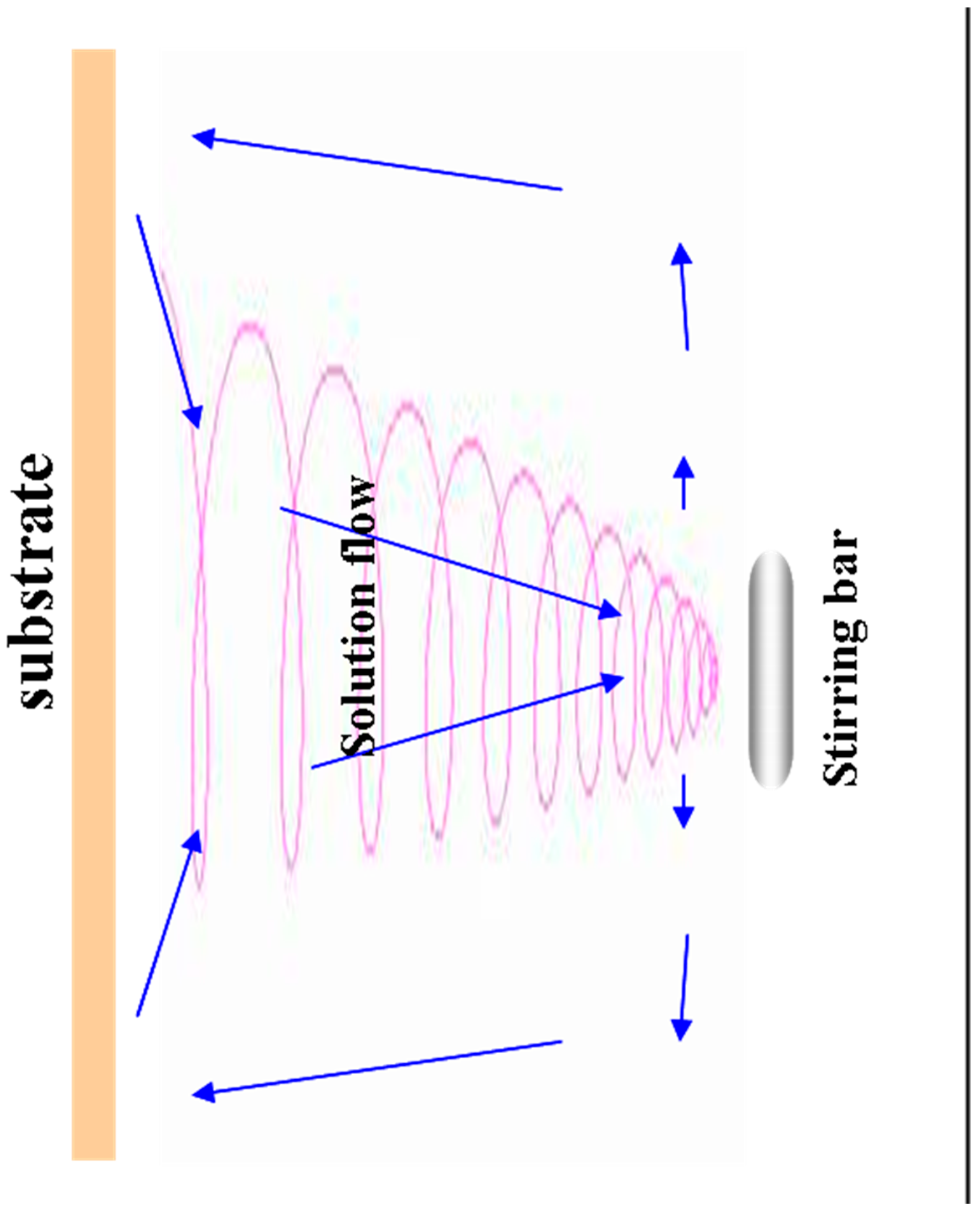
2. Materials and Methods
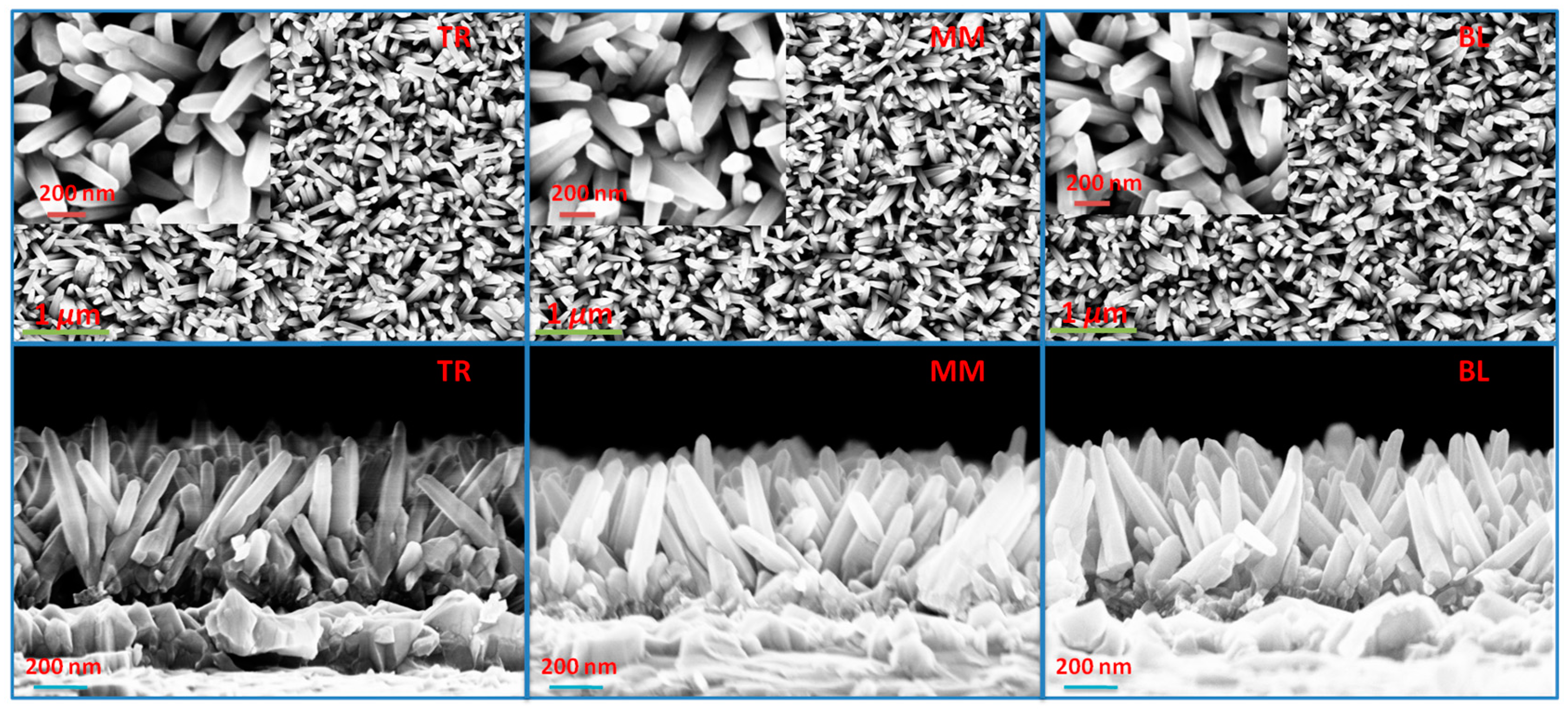
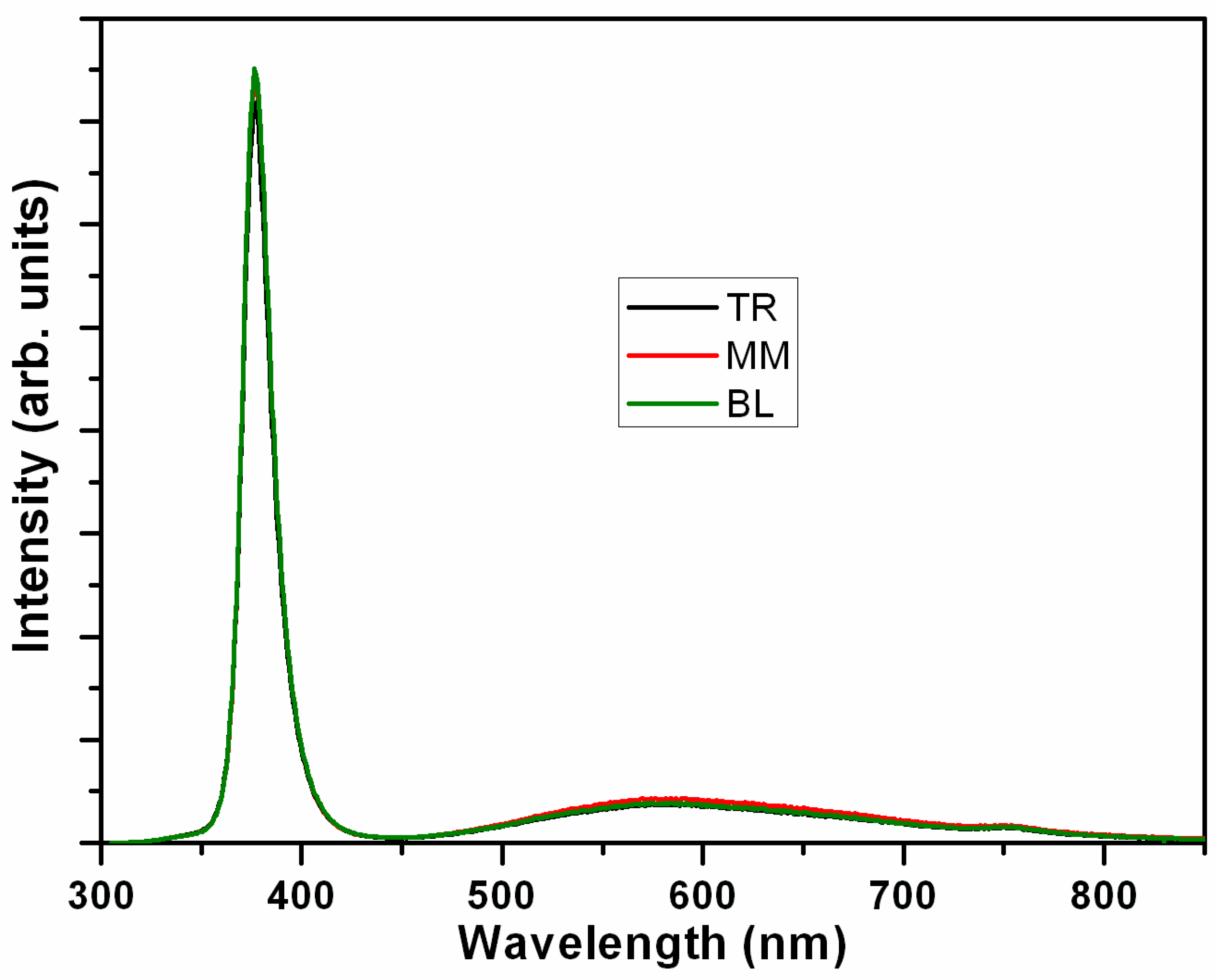
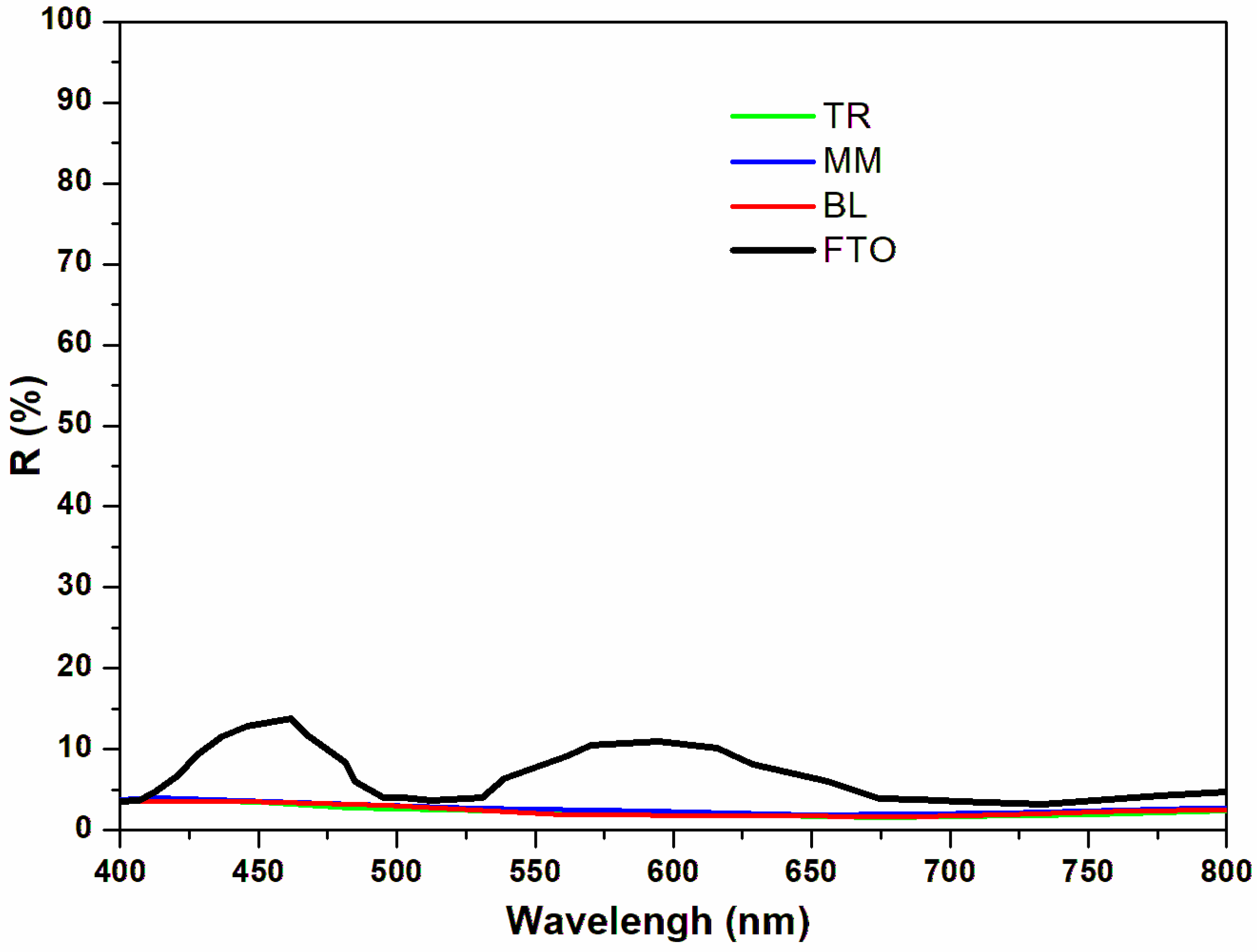
3. Results and Discussion
4. Conclusions
Author Contributions
Funding
Institutional Review Board Statement
Informed Consent Statement
Data Availability Statement
Conflicts of Interest
References
- Green, M.A.; Blakers, A.W.; Shi, J.; Keller, E.M.; Wenham, S.R. High-efficiency silicon solar cells. IEEE Trans. Electron. Dev. 1984, 31, 679–683. [Google Scholar] [CrossRef]
- Shockley, W.; Queisser, H.J. Detailed balance limit of efficiency of p-n junction solar cells. J. Appl. Phys. 1961, 32, 510. [Google Scholar] [CrossRef]
- Gao, Z.L.; Lin, G.L.; Chen, Y.C.; Zheng, Y.P.; Sang, N.; Li, Y.F.; Chen, L.; Li, M.C. Moth-eye nanostructure PDMS films for reducing reflection and retaining flexibility in ultra-thin c-Si solar cells. Solar Energy 2020, 205, 275–281. [Google Scholar] [CrossRef]
- Look, D.C. Recent advances in ZnO material and device. Mater. Sci. Eng. B 2001, 80, 383. [Google Scholar] [CrossRef]
- Desai, A.V.; Haque, M.A. Mechanical properties of ZnO nanowires. Sens. Actuators A Phys. 2007, 134, 169–176. [Google Scholar] [CrossRef]
- Özgür, Ü.; Alivov, Y.A.; Liu, C.; Teke, A.; Reshchikov, M.A.; Doğan, S.; Avrutin, V.; Cho, S.; Morkoc, H.-J. A comprehensive review of ZnO materials and devices. J. Appl. Phys. 2005, 98, 041301. [Google Scholar] [CrossRef]
- Peng, Y.; Que, M.; Lee, H.E.; Bao, R.; Wang, X.; Lu, J.; Yuan, Z.; Li, X.; Tao, J.; Sun, J. Achieving high-resolution pressure mapping via flexible GaN/ZnO nanowire LEDs array by piezo-phototronic effect. Nano Energy 2019, 58, 633–640. [Google Scholar] [CrossRef]
- Zhao, X.; Li, Q.; Xu, L.; Zhang, Z.; Kang, Z.; Liao, Q.; Zhang, Y. Interface engineering in 1D ZnO-based heterostructures for photoelectrical devices. Adv. Funct. Mater. 2022, 32, 2106887. [Google Scholar] [CrossRef]
- Chen, T.; Gao, X.; Zhang, J.Y.; Xu, J.L.; Wang, S.D. Ultrasensitive ZnO nanowire photodetectors with a polymer electret interlayer for minimizing dark current. Adv. Opt. Mater. 2020, 8, 1901289. [Google Scholar] [CrossRef]
- Kumaresan, Y.; Min, G.; Dahiya, A.S.; Ejaz, A.; Shakthivel, D.; Dahiya, R. Kirigami and Mogul-Patterned Ultra-Stretchable High-Performance ZnO Nanowires-Based Photodetector. Adv. Mater. Technol. 2022, 7, 2100804. [Google Scholar] [CrossRef]
- Gullu, H.; Yildiz, D.; Kocyigit, A.; Yıldırım, M. Electrical properties of Al/PCBM: ZnO/p-Si heterojunction for photodiode application. J. Alloys Compd. 2020, 827, 154279. [Google Scholar] [CrossRef]
- Choi, M.S.; Kim, M.Y.; Mirzaei, A.; Kim, H.-S.; Kim, S.-i.; Baek, S.-H.; Chun, D.W.; Jin, C.; Lee, K.H. Selective, sensitive, and stable NO2 gas sensor based on porous ZnO nanosheets. Appl. Surf. Sci. 2021, 568, 150910. [Google Scholar] [CrossRef]
- Wibowo, A.; Marsudi, M.A.; Amal, M.I.; Ananda, M.B.; Stephanie, R.; Ardy, H.; Diguna, L.J. ZnO nanostructured materials for emerging solar cell applications. RSC Adv. 2020, 10, 42838–42859. [Google Scholar] [CrossRef]
- Senol, S.; Ozugurlu, E.; Arda, L. Synthesis, structure and optical properties of (Mn/Cu) co-doped ZnO nanoparticles. J. Alloys Compd. 2020, 822, 153514. [Google Scholar] [CrossRef]
- Tosun, M.; Senol, S.; Arda, L. Effect of Mn/Cu co-doping on the structural, optical and photocatalytic properties of ZnO nanorods. J. Mol. Struct. 2020, 1212, 128071. [Google Scholar] [CrossRef]
- Hendrickson, J.R.; Vangala, S.; Nader, N.; Leedy, K.; Guo, J.; Cleary, J.W. Plasmon resonance and perfect light absorption in subwavelength trench arrays etched in gallium-doped zinc oxide film. Appl. Phys. Lett. 2015, 107, 191906. [Google Scholar] [CrossRef]
- Wilson, S.; Hutley, M. The optical properties of ‘moth eye’ antireflection surfaces. Opt. Acta 1982, 29, 993–1009. [Google Scholar] [CrossRef]
- Aé, L.; Kieven, D.; Chen, J.; Klenk, R.; Rissom, T.; Tang, Y.; Lux-Steiner, M.C. ZnO nanorod arrays as an antireflective coating for Cu(In, Ga)Se2 thin film solar cells. Prog. Photovolt. Res. Appl. 2010, 18, 209–213. [Google Scholar] [CrossRef]
- Lee, Y.J.; Ruby, D.S.; Peters, D.W.; McKenzie, B.B.; Hsu, J.W.P. ZnO nanostructures as efficient antireflection layers in solar cells. Nano Lett. 2008, 8, 1501–1505. [Google Scholar] [CrossRef]
- Leem, J.W.; Joo, D.H.; Yu, J.S. Biomimetic parabola-shaped AZO subwavelength grating structures for efficient antireflection of Si-based solar cells. Sol. Energy Mater. Sol. Cells 2011, 95, 2221–2227. [Google Scholar] [CrossRef]
- Liu, B.; Wang, C.; Bazri, S.; Badruddin, I.A.; Orooji, Y.; Saeidi, S.; Wongwises, S.; Mahian, O. Optical properties and thermal stability evaluation of solar absorbers enhanced by nanostructured selective coating films. Powder Technol. 2021, 377, 939–957. [Google Scholar] [CrossRef]
- Tamulevičius, T.; Laurikėnas, P.; Juodėnas, M.; Mardosaitė, R.; Abakevičienė, B.; Pereyra, C.J.; Račkauskas, S. Antireflection Coatings Based on Randomly Oriented ZnO Nanowires. Sol. RRL 2023, 7, 2201056. [Google Scholar] [CrossRef]
- Chen, J.; Ye, H.; Aé, L.; Tang, Y.; Kieven, D.; Rissom, T.; Neuendorf, J.; Lux-Steiner, M.C. Tapered aluminum-doped vertical zinc oxide nanorod arrays as light coupling layer for solar energy applications. Sol. Energy Mater. Sol. Cells 2011, 95, 1437–1440. [Google Scholar] [CrossRef]
- Zhao, Y.; Tang, Y.; Han, Z. Low-temperature rapid syntheses of high-quality ZnO nanostructure arrays induced by ammonium salt. Chem. Phys. Lett. 2017, 668, 47–55. [Google Scholar] [CrossRef]
- Qu, Y.; Huang, X.; Li, Y.; Lin, G.; Guo, B.; Song, D.; Cheng, Q. Chemical bath deposition produced ZnO nanorod arrays as an antireflective layer in the polycrystalline Si solar cells. J. Alloys Compd. 2017, 698, 719–724. [Google Scholar] [CrossRef]
- Huang, F.; Guo, B.; Li, S.; Fu, J.; Zhang, L.; Lin, G.; Yang, Q.; Cheng, Q. Plasma-produced ZnO nanorod arrays as an antireflective layer in c-Si solar cells. J. Mater. Sci. 2019, 54, 4011–4023. [Google Scholar] [CrossRef]
- Bai, A.; Tang, Y.; Chen, J. Efficient photon capturing in Cu (In, Ga) Se2 thin film solar cells with ZnO nanorod arrays as an antireflective coating. Chem. Phys. Lett. 2015, 636, 134–140. [Google Scholar] [CrossRef]
- Navarrete, E.; Güell, F.; Martinez-Alanis, P.R.; Llobet, E. Chemical vapour deposited ZnO nanowires for detecting ethanol and NO2. J. Alloys Compd. 2022, 890, 161923. [Google Scholar] [CrossRef]
- Swathi, S.; Babu, E.S.; Yuvakkumar, R.; Ravi, G.; Chinnathambi, A.; Alharbi, S.A.; Velauthapillai, D. Branched and unbranched ZnO nanorods grown via chemical vapor deposition for photoelectrochemical water-splitting applications. Ceram. Int. 2021, 47, 9785–9790. [Google Scholar] [CrossRef]
- Huang, M.H.; Wu, Y.; Feick, H.; Tran, N.; Weber, E.; Yang, P. Catalytic growth of zinc oxide nanowires by vapor transport. Adv. Mater. 2001, 13, 113–116. [Google Scholar] [CrossRef]
- Zheng, J.; Jiang, Q.; Lian, J. Synthesis and optical properties of flower-like ZnO nanorods by thermal evaporation method. Appl. Surf. Sci. 2011, 257, 5083–5087. [Google Scholar] [CrossRef]
- Yao, Y.F.; Chou, K.P.; Lin, H.H.; Chen, C.C.; Kiang, Y.W.; Yang, C. Polarity control in growing highly Ga-doped ZnO nanowires with the vapor–liquid–solid process. ACS Appl. Mater. Interfaces 2018, 10, 40764–40772. [Google Scholar] [CrossRef]
- Poornajar, M.; Marashi, P.; Fatmehsari, D.H.; Esfahani, M.K. Synthesis of ZnO nanorods via chemical bath deposition method: The effects of physicochemical factors. Ceram. Int. 2016, 42, 173–184. [Google Scholar] [CrossRef]
- Vessalli, B.A.; Zito, C.A.; Perfecto, T.M.; Volanti, D.P.; Mazon, T. ZnO nanorods/graphene oxide sheets prepared by chemical bath deposition for volatile organic compounds detection. J. Alloys Compd. 2017, 696, 996–1003. [Google Scholar] [CrossRef]
- Pourshaban, E.; Abdizadeh, H.; Golobostanfard, M.R. A close correlation between nucleation sites, growth and final properties of ZnO nanorod arrays: Sol-gel assisted chemical bath deposition process. Ceram. Int. 2016, 42, 14721–14729. [Google Scholar] [CrossRef]
- Tang, Y.; Chen, J.; Greiner, D.; Aé, L.; Baier, R.; Lehmann, J.; Sadewasser, S.; Lux-Steiner, M.C. Fast growth of high work function and high-quality ZnO nanorods from an aqueous solution. J. Phys. Chem. C 2011, 115, 5239–5243. [Google Scholar] [CrossRef]
- Venditti, I.; Barbero, N.; Russo, M.V.; Di Carlo, A.; Decker, F.; Fratoddi, I.; Barolo, C.; Dini, D. Electrodeposited ZnO with squaraine sentisizers as photoactive anode of DSCs. Mater. Res. Express 2014, 1, 015040. [Google Scholar] [CrossRef]
- Bonomo, M.; Naponiello, G.; Venditti, I.; Zardetto, V.; Di Carlo, A.; Dini, D. Electrochemical and photoelectrochemical properties of screen-printed nickel oxide thin films obtained from precursor pastes with different compositions. J. Electrochem. Soc. 2017, 164, H137–H147. [Google Scholar] [CrossRef]
- Jakšić, M.M. Hydrodynamic effects on the macromorphology of electrodeposited zinc and flow visualization: A flat plate electrode in a channel flow cell. J. Electroanal. Chem. Interfacial Electrochem. 1988, 249, 35–62. [Google Scholar] [CrossRef]
- ShakeriHosseinabad, F.; Daemi, S.R.; Momodu, D.; Brett, D.J.; Shearing, P.R.; Roberts, E.P. Influence of flow field design on zinc deposition and performance in a zinc-iodide flow battery. ACS Appl. Mater. Interfaces 2021, 13, 41563–41572. [Google Scholar] [CrossRef]
- Naybour, R. The effect of electrolyte flow on the morphology of zinc electrodeposited from aqueous alkaline solution containing zincate ions. J. Electrochem. Soc. 1969, 116, 520. [Google Scholar] [CrossRef]
- Naybour, R. Morphologies of zinc electrodeposited from zinc-saturated aqueous alkaline solution. Electrochim. Acta 1968, 13, 763–769. [Google Scholar] [CrossRef]
- Lloyd, J.; Sparrow, E.; Eckert, E. Local natural convection mass transfer measurements. J. Electrochem. Soc. 1972, 119, 702. [Google Scholar] [CrossRef]
- Izaki, M.; Omi, T. Electrolyte optimization for cathodic growth of zinc oxide films. J. Electrochem. Soc. 1996, 143, L53. [Google Scholar] [CrossRef]
- Abderrahmane, B.; Djamila, A.; Chaabia, N.; Fodil, R. Improvement of ZnO nanorods photoelectrochemical, optical, structural and morphological characterizations by cerium ions doping. J. Alloys Compd. 2020, 829, 154498. [Google Scholar] [CrossRef]
- Zhang, M.; Reddy, R. Electrical field and current density distribution modeling of aluminum electrodeposition in ionic liquid electrolytes. ECS Trans. 2006, 1, 47. [Google Scholar] [CrossRef]
- Cross, R.; De Souza, M.; Narayanan, E.S. A low temperature combination method for the production of ZnO nanowires. Nanotechnology 2005, 16, 2188. [Google Scholar] [CrossRef] [PubMed]
- Das, A.; Ghosh, S.; Mahapatra, A.D.; Kabiraj, D.; Basak, D. Highly enhanced ultraviolet to visible room temperature photoluminescence emission ratio in Al implanted ZnO nanorods. Appl. Surf. Sci. 2019, 495, 143615. [Google Scholar] [CrossRef]
- Chopra, K.L.; Ranjan, S. Thin Film Solar Cells; Springer: New York, NY, USA, 1983; pp. 515–520. [Google Scholar]
- Moharam, M.G.; Gaylord, T.K. Rigorous coupled-wave analysis of metallic surface-relief gratings. J. Opt. Soc. Am. A 1986, 3, 1780–1787. [Google Scholar] [CrossRef]


| Sample | TL | TM | TR | ML | MM | MR | BL | BM | BR |
|---|---|---|---|---|---|---|---|---|---|
| 1 | 1.46 | 1.1 | 1.54 | 1.21 | 1 | 1.30 | 1.47 | 1.06 | 1.43 |
| 2 | 1.41 | 1.15 | 1.42 | 1.30 | 1 | 1.36 | 1.30 | 1.07 | 1.34 |
| 3 | 1.29 | 1.11 | 1.30 | 1.18 | 1 | 1.13 | 1.16 | 0.95 | 1.16 |
| Sample | TL | TM | TR | ML | MM | MR | BL | BM | BR |
|---|---|---|---|---|---|---|---|---|---|
| 2 | 1.41 | 1.15 | 1.42 | 1.30 | 1 | 1.36 | 1.30 | 1.07 | 1.34 |
| 4 | 1.02 | 0.93 | 1.22 | 0.99 | 1 | 1.12 | 0.87 | 0.96 | 0.96 |
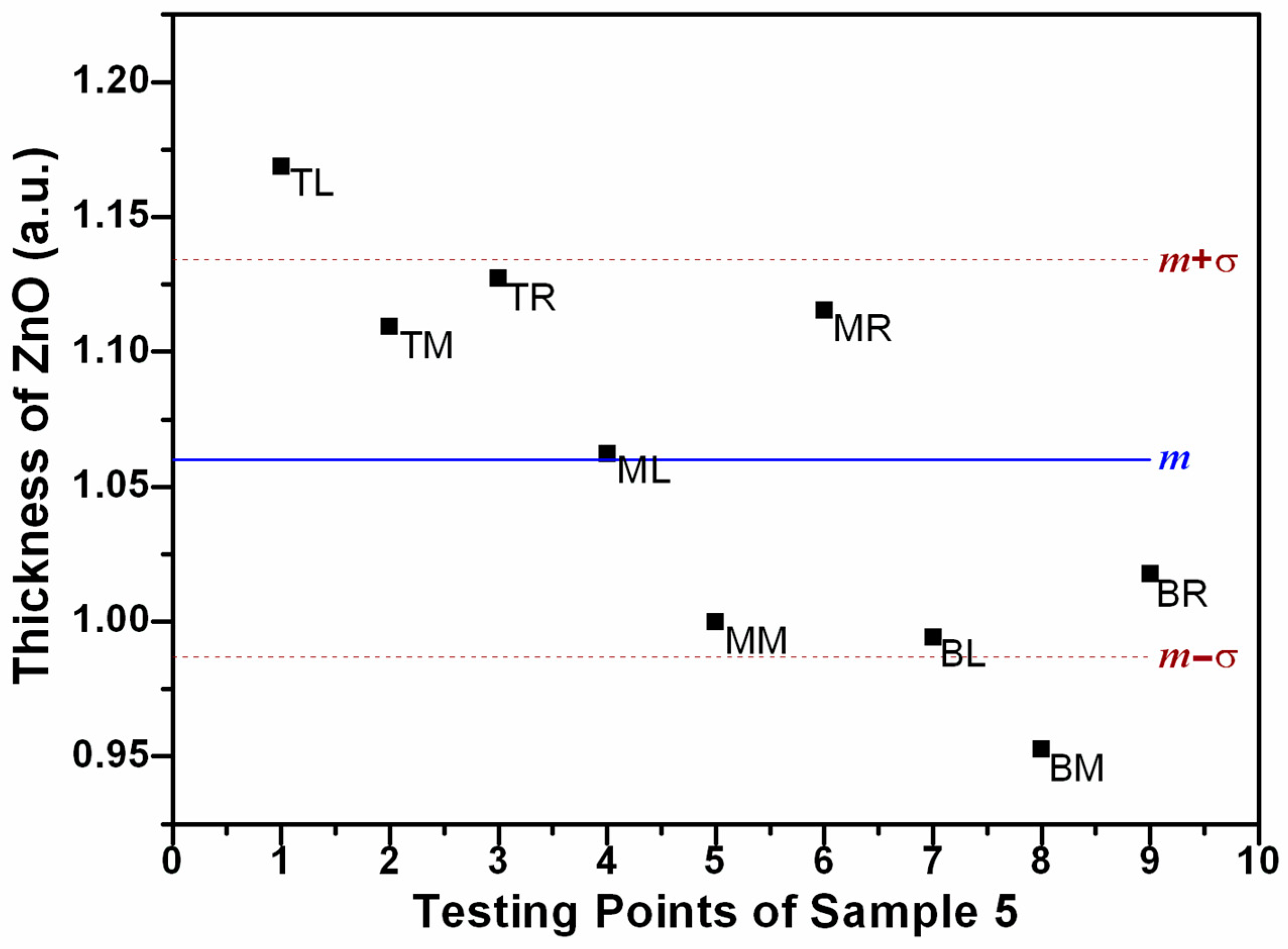
| Sample | TL | TM | TR | ML | MM | MR | BL | BM | BR |
|---|---|---|---|---|---|---|---|---|---|
| 5 | 1.16 | 1.11 | 1.12 | 1.06 | 1 | 1.11 | 0.99 | 0.95 | 1.02 |
Disclaimer/Publisher’s Note: The statements, opinions and data contained in all publications are solely those of the individual author(s) and contributor(s) and not of MDPI and/or the editor(s). MDPI and/or the editor(s) disclaim responsibility for any injury to people or property resulting from any ideas, methods, instructions or products referred to in the content. |
© 2024 by the authors. Licensee MDPI, Basel, Switzerland. This article is an open access article distributed under the terms and conditions of the Creative Commons Attribution (CC BY) license (https://creativecommons.org/licenses/by/4.0/).
Share and Cite
Zhao, Y.; Li, K.; Hu, Y.; Hou, X.; Lin, F.; Tang, J.; Tang, X.; Xing, X.; Zhao, X.; Zhu, H.; et al. The Effect of the Solution Flow and Electrical Field on the Homogeneity of Large-Scale Electrodeposited ZnO Nanorods. Materials 2024, 17, 1241. https://doi.org/10.3390/ma17061241
Zhao Y, Li K, Hu Y, Hou X, Lin F, Tang J, Tang X, Xing X, Zhao X, Zhu H, et al. The Effect of the Solution Flow and Electrical Field on the Homogeneity of Large-Scale Electrodeposited ZnO Nanorods. Materials. 2024; 17(6):1241. https://doi.org/10.3390/ma17061241
Chicago/Turabian StyleZhao, Yanmin, Kexue Li, Ying Hu, Xiaobing Hou, Fengyuan Lin, Jilong Tang, Xin Tang, Xida Xing, Xiao Zhao, Haibin Zhu, and et al. 2024. "The Effect of the Solution Flow and Electrical Field on the Homogeneity of Large-Scale Electrodeposited ZnO Nanorods" Materials 17, no. 6: 1241. https://doi.org/10.3390/ma17061241