
Destabilization of the Charge Density Wave and the Absence of Superconductivity in ScV6Sn6 under High Pressures up to 11 GPa

 , , , , and
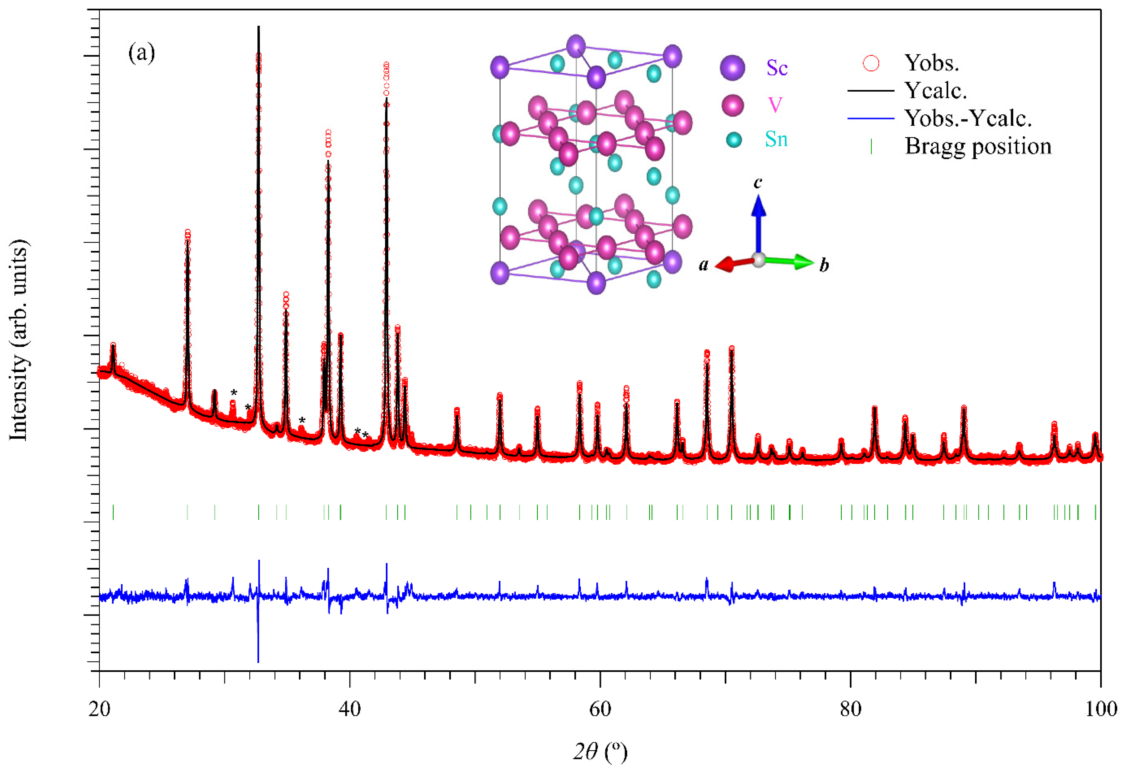
Abstract
:1. Introduction
2. Materials and Methods
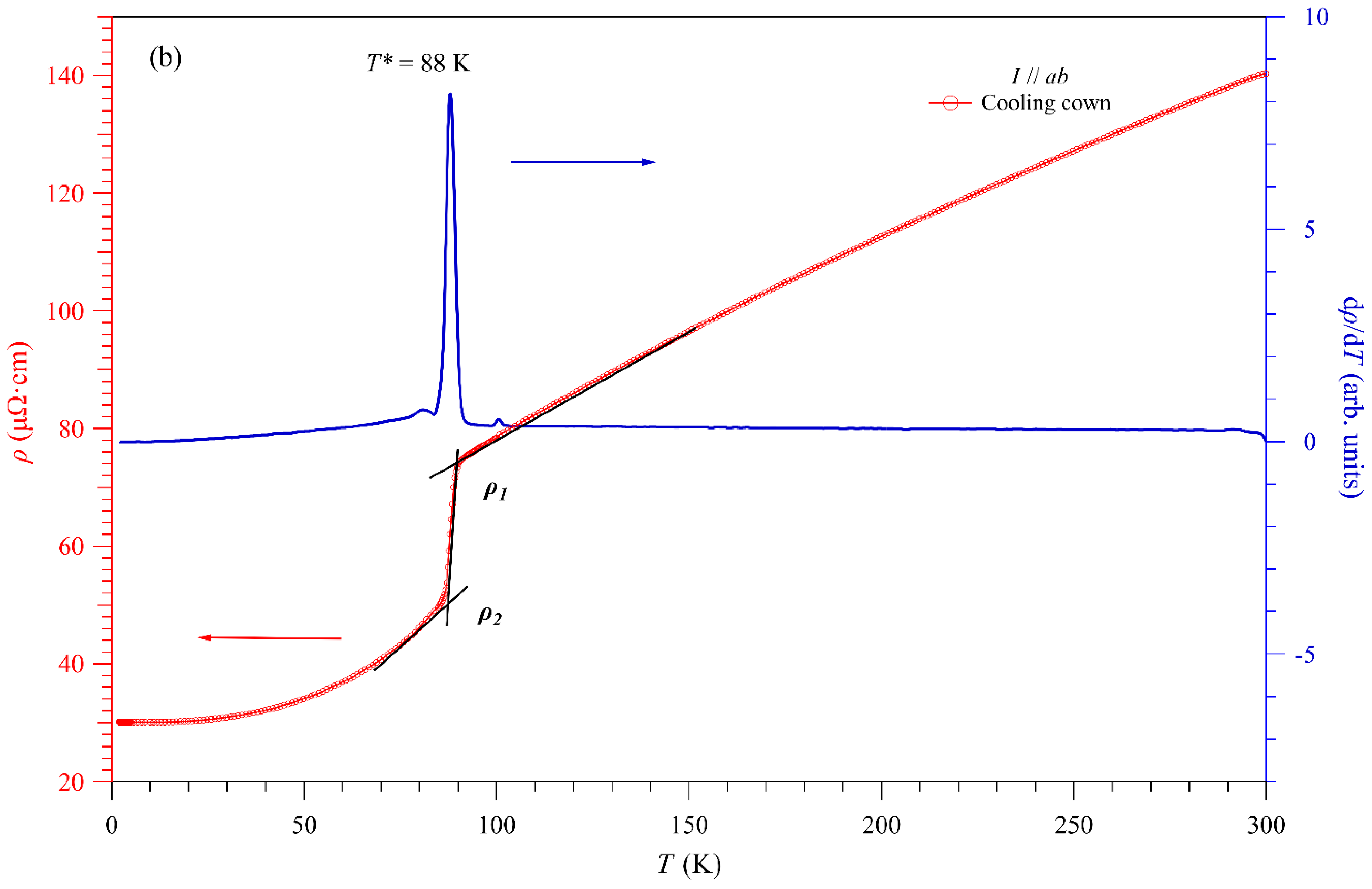
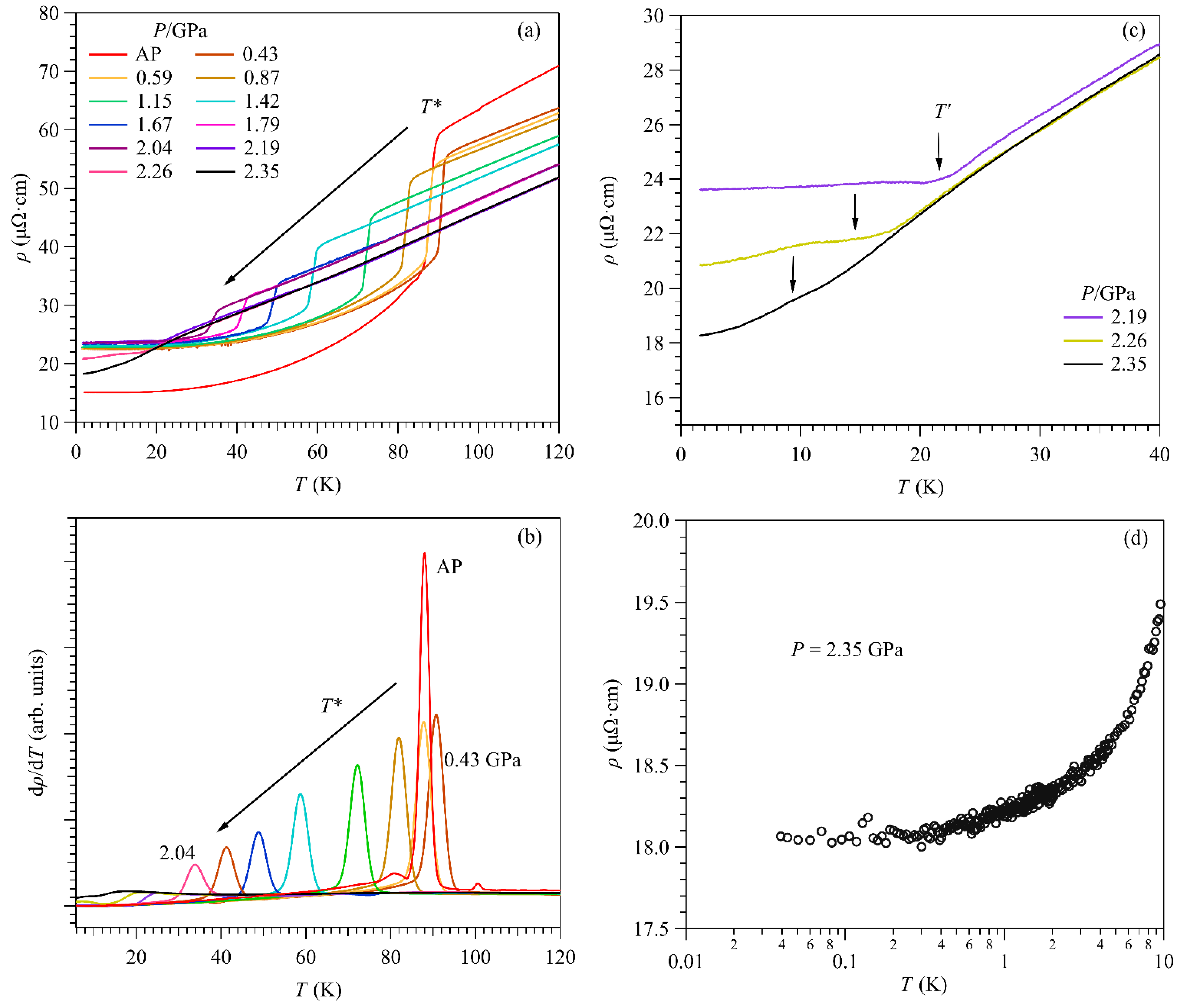
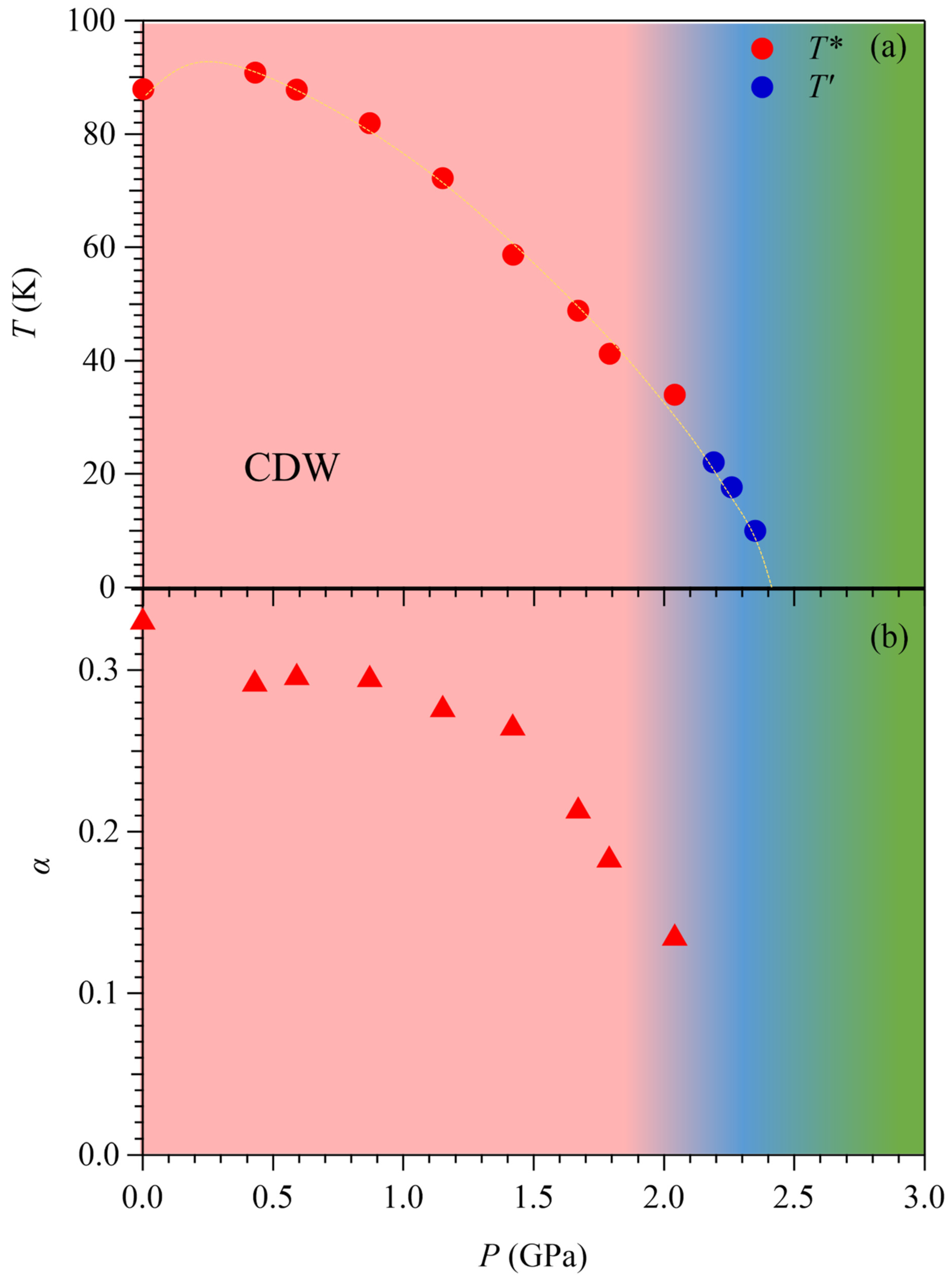
3. Results
4. Discussion
5. Conclusions
Author Contributions
Funding
Institutional Review Board Statement
Informed Consent Statement
Data Availability Statement
Acknowledgments
Conflicts of Interest
References
- Park, T.; Ye, M.; Balents, L. Electronic instabilities of kagome metals: Saddle points and Landau theory. Phys. Rev. B 2021, 104, 035142. [Google Scholar] [CrossRef]
- Guo, H.M.; Franz, M. Topological insulator on the kagome lattice. Phys. Rev. B 2009, 80, 113102. [Google Scholar] [CrossRef] [Green Version]
- Mazin, I.I.; Jeschke, H.; Lechermann, F.; Lee, H.; Fink, M.; Thomale, R.; Valentí, R. Theoretical prediction of a strongly correlated Dirac metal. Nat. Commun. 2014, 5, 4261. [Google Scholar] [CrossRef] [PubMed] [Green Version]
- Tang, E.; Mei, J.-W.; Wen, X.-G. High-Temperature Fractional Quantum Hall States. Phys. Rev. Lett. 2011, 106, 236802. [Google Scholar] [CrossRef] [Green Version]
- Wang, W.S.; Li, Z.Z.; Xiang, Y.Y.; Wang, Q.H. Competing electronic orders on kagome lattices at van Hove filling. Phys. Rev. B 2013, 87, 115135. [Google Scholar] [CrossRef] [Green Version]
- Wu, X.; Schwemmer, T.; Muller, T.; Consiglio, A.; Sangiovanni, G.; Di Sante, D.; Iqbal, Y.; Hanke, W.; Schnyder, A.P.; Denner, M.M.; et al. Nature of Unconventional Pairing in the Kagome Superconductors AV3Sb5 (A = K, Rb, Cs). Phys. Rev. Lett. 2021, 127, 177001. [Google Scholar] [CrossRef] [PubMed]
- Yu, S.L.; Li, J.X. Chiral superconducting phase and chiral spin-density-wave phase in a Hubbard model on the kagome lattice. Phys. Rev. B 2012, 85, 144402. [Google Scholar] [CrossRef] [Green Version]
- Neupert, T.; Denner, M.M.; Yin, J.X.; Thomale, R.; Hasan, M.Z. Charge Order and Superconductivity in Kagome Materials. Nat. Phys. 2022, 18, 137. [Google Scholar] [CrossRef]
- Singh, R.R.; Huse, D.A. Ground State of the Spin-1/2 Kagome-Lattice Heisenberg Antiferromagnet. Phys. Rev. B 2007, 76, 180407. [Google Scholar] [CrossRef] [Green Version]
- Zhao, C.C.; Wang, L.S.; Xia, W.; Yin, Q.W.; Ni, J.M.; Huang, Y.Y.; Tu, C.P.; Tao, Z.C.; Tu, Z.J.; Gong, C.S.; et al. Nodal Superconductivity and Superconducting Domes in the Topological Kagome Metal CsV3Sb5. arXiv 2021, arXiv:2102.08356. [Google Scholar]
- Chen, H.; Hu, B.; Ye, Y.; Yang, H.; Gao, H. Superconductivity and unconventional density waves in vanadium-based kagome materials AV3Sb5. Chin. Phys. B 2022, 31, 1088. [Google Scholar] [CrossRef]
- Chen, K.Y.; Wang, N.N.; Yin, Q.W.; Gu, Y.H.; Jiang, K.; Tu, Z.J.; Gong, C.S.; Uwatoko, Y.; Sun, J.P.; Lei, H.C.; et al. Double Superconducting Dome and Triple Enhancement of Tc in the Kagome Superconductor CsV3Sb5 under High Pressure. Phys. Rev. Lett. 2021, 126, 247001. [Google Scholar] [CrossRef] [PubMed]
- Xu, H.S.; Yan, Y.J.; Yin, R.; Xia, W.; Fang, S.; Chen, Z.; Li, Y.; Yang, W.; Guo, Y.; Feng, D.L. Multiband Superconductivity with Sign-Preserving Order Parameter in Kagome Superconductor CsV3Sb5. Phys. Rev. Lett. 2021, 127, 187004. [Google Scholar] [CrossRef]
- Ortiz, B.R.; Gomes, L.C.; Morey, J.R.; Winiarski, M.; Bordelon, M.; Mangum, J.S.; Oswald, I.W.H.; Rodriguez-Rivera, J.A.; Neilson, J.R.; Wilson, S.D.; et al. New Kagome Prototype Materials: Discovery of KV3Sb5, RbV3Sb5, and CsV3Sb5. Phys. Rev. Mater. 2019, 3, 094407. [Google Scholar] [CrossRef]
- Jiang, Y.X.; Yin, J.X.; Denner, M.M.; Shumiya, N.; Ortiz, B.R.; Xu, G.; Guguchia, Z.; He, J.; Hossain, S.; Liu, X.; et al. Unconventional chiral charge order in kagome superconductor KV3Sb5. Nat. Mater. 2021, 20, 1353–1357. [Google Scholar] [CrossRef]
- Nguyen, T.; Li, M. Electronic Properties of Correlated Kagomé Metals AV3Sb5 (A = K, Rb, and Cs): A Perspective. J. App. Phys. 2022, 131, 060901. [Google Scholar] [CrossRef]
- Ortiz, B.R.; Teicher, S.M.L.; Hu, Y.; Zuo, J.L.; Sarte, P.M.; Schueller, E.C.; Abeykoon, A.M.M.; Krogstad, M.J.; Rosenkranz, S.; Osborn, R.; et al. CsV3Sb5: A Z2 Topological Kagome Metal with a Superconducting Ground State. Phys. Rev. Lett. 2020, 125, 247002. [Google Scholar] [CrossRef]
- Yin, Q.; Tu, Z.; Gong, C.; Fu, Y.; Yan, S.; Lei, H. Superconductivity and Normal-State Properties of Kagome Metal RbV3Sb5 Single Crystals. Chin. Phys. Lett. 2021, 38, 037403. [Google Scholar] [CrossRef]
- Chen, H.; Yang, H.; Hu, B.; Zhao, Z.; Yuan, J.; Xing, Y.; Qian, G.; Huang, Z.; Li, G.; Ye, Y.; et al. Roton pair density wave in a strong-coupling kagome superconductor. Nature 2021, 599, 222–228. [Google Scholar] [CrossRef] [PubMed]
- Mielke, C., III; Das, D.; Yin, J.-X.; Liu, H.; Gupta, R.; Jiang, Y.-X.; Medarde, M.; Wu, X.; Lei, H.C.; Chang, J.; et al. Time-Reversal Symmetry-Breaking Charge Order in a Kagome Superconductor. Nature 2021, 602, 245. [Google Scholar] [CrossRef] [PubMed]
- Li, H.; Zhang, T.T.; Yilmaz, T.; Pai, Y.Y.; Marvinney, C.E.; Said, A.; Yin, Q.W.; Gong, C.S.; Tu, Z.J.; Vescovo, E.; et al. Observation of Unconventional Charge Density Wave without Acoustic Phonon Anomaly in Kagome Superconductors AV3Sb5 (A=Rb, Cs). Phys. Rev. X 2021, 11, 031050. [Google Scholar] [CrossRef]
- Liang, Z.; Hou, X.; Zhang, F.; Ma, W.; Wu, P.; Zhang, Z.; Yu, F.; Ying, J.J.; Jiang, K.; Shan, L.; et al. Three-Dimensional Charge Density Wave and Surface-Dependent Vortex-Core States in a Kagome Superconductor CsV3Sb5. Phys. Rev. X 2021, 11, 031026. [Google Scholar] [CrossRef]
- Miao, H.; Li, H.X.; Meier, W.R.; Huon, A.; Lee, H.N.; Said, A.; Lei, H.C.; Ortiz, B.R.; Wilson, S.D.; Yin, J.X.; et al. Geometry of the Charge Density Wave in the Kagome Metal AV3Sb5. Phys. Rev. B 2021, 104, 195132. [Google Scholar] [CrossRef]
- Ortiz, B.R.; Sarte, P.M.; Kenney, E.M.; Graf, M.J.; Teicher, S.M.L.; Seshadri, R.; Wilson, S.D. Superconductivity in the Z2 Kagome Metal KV3Sb5. Phys. Rev. Mater. 2021, 5, 034801. [Google Scholar] [CrossRef]
- Wang, N.N.; Chen, K.Y.; Yin, Q.W.; Ma, Y.N.N.; Pan, B.Y.; Yang, X.; Ji, X.Y.; Wu, S.L.; Shan, P.F.; Xu, S.X.; et al. Competition between Charge-Density-Wave and Superconductivity in the Kagome Metal RbV3Sb5. Phys. Rev. Res. 2021, 3, 043018. [Google Scholar] [CrossRef]
- Yu, F.H.; Ma, D.H.; Zhuo, W.Z.; Liu, S.Q.; Wen, X.K.; Lei, B.; Ying, J.J.; Chen, X.H. Unusual competition of superconductivity and charge-density-wave state in a compressed topological kagome metal. Nat. Commun. 2021, 12, 3645. [Google Scholar] [CrossRef]
- Luo, J.; Zhao, Z.; Zhou, Y.Z.; Yang, J.; Fang, A.F.; Yang, H.T.; Gao, H.J.; Zhou, R.; Zheng, G.-Q. Possible star-of-David pattern charge density wave with additional modulation in the kagome superconductor CsV3Sb5. NPJ Quantum Mater. 2022, 7, 30. [Google Scholar] [CrossRef]
- Du, F.; Li, R.; Luo, S.; Gong, Y.; Li, Y.; Jiang, S.; Ortiz, B.R.; Liu, Y.; Xu, X.; Wilson, S.D.; et al. Superconductivity modulated by structural phase transitions in pressurized vanadium-based kagome metals. Phys. Rev. B 2022, 106, 024516. [Google Scholar] [CrossRef]
- Duan, W.; Nie, Z.; Luo, S.; Yu, F.; Ortiz, B.R.; Yin, L.; Su, H.; Du, F.; Wang, A.; Chen, Y.; et al. Nodeless superconductivity in the kagome metal CsV3Sb5. Sci. China Ser. G: Phys. Mech. Astron. 2021, 64, 107462. [Google Scholar] [CrossRef]
- Gupta, R.; Das, D.; Iii, C.H.M.; Guguchia, Z.; Shiroka, T.; Baines, C.; Bartkowiak, M.; Luetkens, H.; Khasanov, R.; Yin, Q.; et al. Microscopic evidence for anisotropic multigap superconductivity in the CsV3Sb5 kagome superconductor. NPJ Quantum Mater. 2022, 7, 49. [Google Scholar] [CrossRef]
- Zhang, Z.; Chen, Z.; Zhou, Y.; Yuan, Y.; Wang, S.; Wang, J.; Yang, H.; An, C.; Zhang, L.; Zhu, X.; et al. Pressure-Induced Reemergence of Superconductivity in the Topological Kagome Metal CsV3Sb5. Phys. Rev. B 2021, 103, 224513. [Google Scholar] [CrossRef]
- Zhu, C.; Yang, X.; Xia, W.; Yin, Q.; Wang, L.; Zhao, C.; Dai, D.; Tu, C.; Song, B.; Tao, Z.; et al. Double-Dome Superconductivity under Pressure in the V-Based Kagome Metals AV3Sb5 (A = Rb and K). Phys. Rev. B 2022, 105, 094507. [Google Scholar] [CrossRef]
- Pokharel, G.; Teicher, S.M.L.; Ortiz, B.R.; Sarte, P.M.; Wu, G.; Peng, S.; He, J.; Seshadri, R.; Wilson, S.D. Electronic Properties of the Topological Kagome Metals YV6Sn6 and GdV6Sn6. Phys. Rev. B 2021, 104, 060901. [Google Scholar] [CrossRef]
- Zhang, X.; Liu, Z.; Cui, Q.; Wang, N.; Shi, L.; Zhang, H.; Dong, X.; Sun, J.; Dun, Z.; Cheng, J. Electronic and Magnetic Properties of Intermetallic Kagome Magnets RV6Sn6 (R = Tb-Tm). Phys. Rev. Mater. 2022, 6, 105001. [Google Scholar] [CrossRef]
- Hu, Y.; Wu, X.; Yang, Y.; Gao, S.; Plumb, N.C.; Schnyder, A.P.; Xie, W.; Ma, J.; Shi, M. Tunable Topological Dirac Surface States and Van Hove Singularities in Kagome Metal GdV6Sn6. arXiv 2022, arXiv:2205.15927. [Google Scholar]
- Peng, S.; Han, Y.; Pokharel, G.; Shen, J.; Li, Z.; Hashimoto, M.; Lu, D.; Ortiz, B.R.; Luo, Y.; Li, H.; et al. Realizing Kagome Band Structure in Two-Dimensional Kagome Surface States of RV6Sn6 (R = Gd, Ho). Phys. Rev. Lett. 2021, 127, 266401. [Google Scholar] [CrossRef] [PubMed]
- Arachchige, H.W.S.; Meier, W.R.; Marshall, M.; Matsuoka, T.; Xue, R.; McGuire, M.A.; Hermann, R.P.; Cao, H.; Mandrus, D. Charge Density Wave in Kagome Lattice Intermetallic ScV6Sn6. arXiv 2022, arXiv:2205.04582. [Google Scholar]
- Liu, Z.Y.; Li, J.; Zhang, J.F.; Yang, P.T.; Zhang, S.; Chen, G.F.; Uwatoko, Y.; Yang, H.X.; Sui, Y.; Liu, K.; et al. Quasi-one-dimensional superconductivity in the pressurized charge-density-wave conductor HfTe3. NPJ Quantum Mater. 2021, 6, 90. [Google Scholar] [CrossRef]
- Xu, S.; Yang, P.; Chen, K.; Liu, Z.; Cui, W.; Hu, Q.; Sun, J.; Ang, R.; Uwatoko, Y.; Wang, B. Superconducting Phase Diagram and the Evolution of Electronic Structure across Charge Density Wave in Underdoped 1T−CuδTiSe2 under Hydrostatic Pressure. Phys. Rev. B 2021, 104, 134503. [Google Scholar] [CrossRef]
- Cheng, J.; Matsubayashi, K.; Nagasaki, S.; Hisada, A.; Hirayama, T.; Hedo, M.; Kägi, H.; Uwatoko, Y. Integrated-fin gasket for palm cubic-anvil high pressure apparatus. Rev. Sci. Instrum. 2014, 85, 093907. [Google Scholar] [CrossRef] [PubMed]
- Yamaya, K.; Yoneda, M.; Yasuzuka, S.; Okajima, Y.; Tanda, S. The effect of pressure on the charge-density wave and superconductivity in ZrTe3. J. Phys. Condens. Matter 2002, 14, 10767–10770. [Google Scholar] [CrossRef]
- Banerjee, A.; Garg, A.; Ghosal, A. Emergent superconductivity upon disordering a charge density wave ground state. Phys. Rev. B 2018, 98, 104206. [Google Scholar] [CrossRef] [Green Version]
- Shen, B.; Du, F.; Li, R.; Thamizhavel, A.; Smidman, M.; Nie, Z.Y.; Luo, S.S.; Le, T.; Hossain, Z.; Yuan, H.Q. Evolution of Charge Density Wave Order and Superconductivity under Pressure in LaPt2Si2. Phys. Rev. B 2020, 101, 144501. [Google Scholar] [CrossRef]
- Sahoo, S.; Dutta, U.; Harnagea, L.; Sood, A.K.; Karmakar, S. Pressure-Induced Suppression of Charge Density Wave and Emergence of Superconductivity in 1T−VSe2. Phys. Rev. B 2020, 101, 014514. [Google Scholar] [CrossRef] [Green Version]
- Xia, W.; Wu, J.; Li, Z.; Yuan, J.; An, C.; Wang, X.; Yu, N.; Zou, Z.; Liu, G.; Zhou, C.; et al. Pressure-Induced Superconductivity Reentrant in Transition Metal Dichalcogenide TiSe2. arXiv 2022, arXiv:2202.06244. [Google Scholar]
- Shi, L.F.; Liu, Z.Y.; Li, J.; Zhang, X.X.; Wang, N.N.; Cui, Q.; Chen, K.Y.; Liu, Q.Y.; Yang, P.T.; Sun, J.P.; et al. Pressure-driven superconducting dome in the vicinity of CDW in the pyrite-type superconductor CuS2. Phys. Rev. Mater. 2022, 6, 014802. [Google Scholar] [CrossRef]
- Xu, S.; Gao, J.; Liu, Z.; Chen, K.; Yang, P.; Tian, S.; Gong, C.; Sun, J.; Xue, M.; Gouchi, J.; et al. Effects of Disorder and Hydrostatic Pressure on Charge Density Wave and Superconductivity in 2H−TaS2. Phys. Rev. B 2021, 103, 224509. [Google Scholar] [CrossRef]
- Kang, M.; Fang, S.; Yoo, J.; Ortiz, B.R.; Oey, Y.; Ryu, S.H.; Kim, J.; Jozwiak, C.; Bostwick, A.; Rotenberg, E.; et al. Microscopic Structure of Three-Dimensional Charge Order in Kagome Superconductor AV3Sb5 and Its Tunability. arXiv 2022, arXiv:2202.01902. [Google Scholar]
- Ortiz, B.R.; Teicher, S.M.; Kautzsch, L.; Sarte, P.M.; Ratcliff, N.; Harter, J.; Harter, J.; Ruff, J.P.C.; Seshadri, R.; Wilson, S.D. Fermi Surface Mapping and the Nature of Charge-Density-Wave Order in the Kagome Superconductor CsV3Sb5. Phys. Rev. X 2021, 11, 041030. [Google Scholar] [CrossRef]
- Nie, L.; Sun, K.; Ma, W.; Song, D.; Zheng, L.; Liang, Z.; Wu, P.; Yu, F.; Li, J.; Shan, M.; et al. Charge-density-wave-driven electronic nematicity in a kagome superconductor. Nature 2022, 604, 59–64. [Google Scholar] [CrossRef]
- Wang, Z.; Jiang, Y.-X.; Yin, J.-X.; Li, Y.; Wang, G.-Y.; Huang, H.-L.; Shao, S.; Liu, J.; Zhu, P.; Shumiya, N.; et al. Electronic Nature of Chiral Charge Order in the Kagome Superconductor CsV3Sb5. Phys. Rev. B 2021, 104, 075148. [Google Scholar] [CrossRef]
- Shi, M.; Yu, F.; Yang, Y.; Meng, F.; Bin Lei, B.; Luo, Y.; Sun, Z.; He, J.; Wang, R.; Jiang, Z.; et al. A new class of bilayer kagome lattice compounds with Dirac nodal lines and pressure-induced superconductivity. Nat. Commun. 2022, 13, 2773. [Google Scholar] [CrossRef] [PubMed]


Publisher’s Note: MDPI stays neutral with regard to jurisdictional claims in published maps and institutional affiliations. |
© 2022 by the authors. Licensee MDPI, Basel, Switzerland. This article is an open access article distributed under the terms and conditions of the Creative Commons Attribution (CC BY) license (https://creativecommons.org/licenses/by/4.0/).
Share and Cite
Zhang, X.; Hou, J.; Xia, W.; Xu, Z.; Yang, P.; Wang, A.; Liu, Z.; Shen, J.; Zhang, H.; Dong, X.; et al. Destabilization of the Charge Density Wave and the Absence of Superconductivity in ScV6Sn6 under High Pressures up to 11 GPa. Materials 2022, 15, 7372. https://doi.org/10.3390/ma15207372
Zhang X, Hou J, Xia W, Xu Z, Yang P, Wang A, Liu Z, Shen J, Zhang H, Dong X, et al. Destabilization of the Charge Density Wave and the Absence of Superconductivity in ScV6Sn6 under High Pressures up to 11 GPa. Materials. 2022; 15(20):7372. https://doi.org/10.3390/ma15207372
Chicago/Turabian StyleZhang, Xiaoxiao, Jun Hou, Wei Xia, Zhian Xu, Pengtao Yang, Anqi Wang, Ziyi Liu, Jie Shen, Hua Zhang, Xiaoli Dong, and et al. 2022. "Destabilization of the Charge Density Wave and the Absence of Superconductivity in ScV6Sn6 under High Pressures up to 11 GPa" Materials 15, no. 20: 7372. https://doi.org/10.3390/ma15207372