Article

Control of the Nucleation Density of Molybdenum Disulfide in Large-Scale Synthesis Using Chemical Vapor Deposition

1
College of Electronic Engineering, South China Agricultural University, Guangzhou 510642, China
2
State Key Laboratory of Silicon Materials, School of Materials Science and Engineering, Zhejiang University, Hangzhou 310027, China
*
Author to whom correspondence should be addressed.
Materials 2018, 11(6), 870; https://doi.org/10.3390/ma11060870
Submission received: 28 April 2018 / Revised: 17 May 2018 / Accepted: 20 May 2018 / Published: 23 May 2018
(This article belongs to the Special Issue Recent Advances in 2D Nanomaterials)

Abstract

:
Atmospheric pressure chemical vapor deposition (CVD) is presently a promising approach for preparing two-dimensional (2D) MoS2 crystals at high temperatures on SiO2/Si substrates. In this work, we propose an improved CVD method without hydrogen, which can increase formula flexibility by controlling the heating temperature of MoO3 powder and sulfur powder. The results show that the size and coverage of MoS2 domains vary largely, from discrete triangles to continuous film, on substrate. We find that the formation of MoS2 domains is dependent on the nucleation density of MoS2. Laminar flow theory is employed to elucidate the cause of the different shapes of MoS2 domains. The distribution of carrier gas speeds at the substrate surface leads to a change of nucleation density and a variation of domain morphology. Thus, nucleation density and domain morphology can be actively controlled by adjusting the carrier gas flow rate in the experimental system. These results are of significance for understanding the growth regulation of 2D MoS2 crystals.

1. Introduction

As one kind of transition metal dichalcogenide (TMD) [1], molybdenum disulfide (MoS2) is the best known material for two-dimensional (2D) crystal research after graphene [2]. With its reduced number of layers, MoS2 exhibits many excellent properties [3,4], such as good optical transparency [5], high electron mobility (up to 200 cm2/V·s), and direct band-gap structure (Eg = 1.8 eV) [6]. It can be employed to fabricate field effect transistors (FETs) with a high current on/off ratio [5,7], sensitive photodetectors [8,9], light emitting diodes (LEDs) [10,11], and heterojunction solar cells [12,13]. Thus, due to its unique semiconductor properties and wide applications, 2D MoS2 attracts great attention. It is considered a potential candidate in atomic-scale semiconductor science [14,15].
Recently, the main preparation methods of MoS2 have included hydrothermal synthesis [16], tape auxiliary mechanical exfoliation [17], liquid-phase exfoliation [14], physical vapor deposition (PVD) [18], and chemical vapor deposition (CVD) [19]. Compared with other methods, CVD is an efficient method to massively synthesize an MoS2 coating. The CVD method can also alter the shape of MoS2 domains from triangular nanosheets to continuous films by controlling synthesis parameters, such as the quantity of the reactants, the temperature of precursors, and the carrier gas flow rate. Previous studies have proven that the nucleation density of MoS2 played a key role in the deposition process, leading to the quality and shape control of MoS2 domains [20,21,22,23,24,25]. It is reported that, before the growth of MoS2, adding a “seed layer” on the substrates can adjust the nucleation density of MoS2 and control the shape of MoS2 domains [20,21,22]. With its hexagonal lattice structure, graphene can be chosen as a seed layer to form MoS2 nuclei. However, the pre-treatment process of adding a seed layer requires the addition of steps to the CVD method, and part of the seed material is toxic [21]. The rest of the seed compound will introduce an unfavorable factor in changing the electronic or optical characteristics of MoS2 samples. Hence, it is necessary to find a simplified process to control the nucleation density of MoS2.
In this paper, we propose a simple CVD method at atmospheric pressure without hydrogen which can increase formula flexibility by controlling the heating temperature of MoO3 powder and sulfur powder. The results show that the size of MoS2 grown domains is 10 μm with fast growth. The shape of MoS2 domains vary widely, from discrete darts and triangles to continuous film, on substrate. We deduce that the carrier flow rate distribution in the quartz tube leads to a variation in the nucleation density of MoS2, resulting in the eventual shape distribution of MoS2 domains. Therefore, controlling the carrier gas flow rate can be an effective approach to controlling the shape and coverage of MoS2 domains in the CVD method. These results are of significance for understanding the growth regulation of 2D MoS2.

2. Materials and Methods

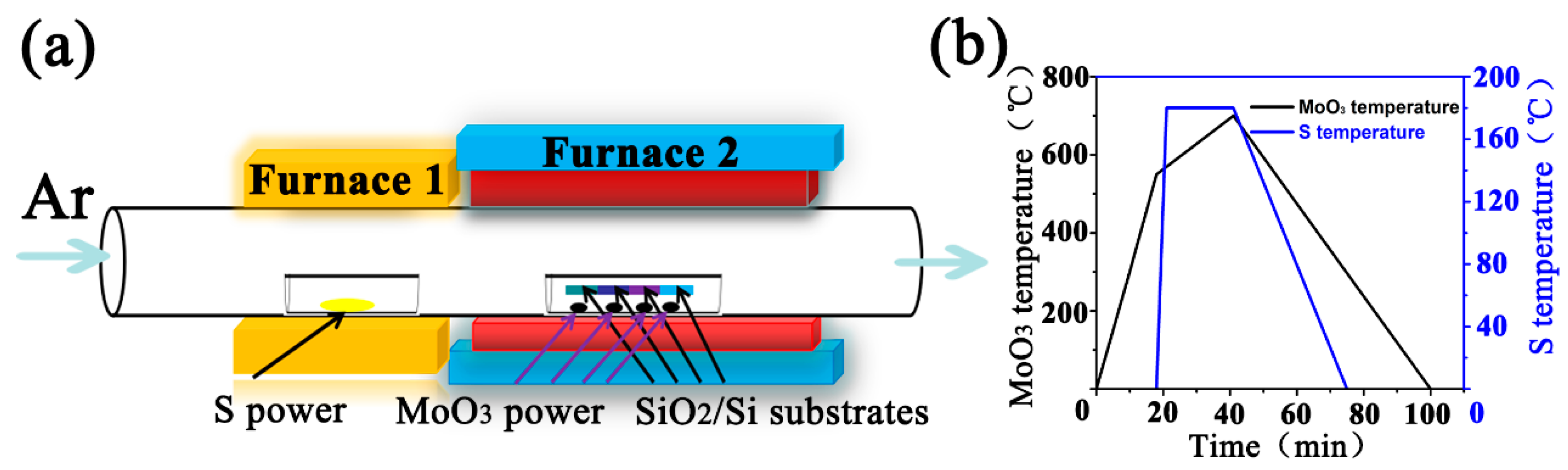
2.1. Synthesis Precursor

As shown in Figure 1, high-purity sulfur (S) and molybdenum trioxide (MoO3) powder (Alfa Aesar, >99.9%) were used as raw materials for the synthesis of MoS2. SiO2/Si substrates were ultra-sonically cleaned with alcohol and deionized water. MoO3 powder (0.1 mg) was grounded into four average parts by SiO2/Si substrates and placed in a double-open quartz boat a small distance apart from another. Another four pieces of clean SiO2/Si substrates were placed on the top of quartz boat, which were seated face-down to the MoO3 powder. All of them were situated in the center position of furnace 2. Then, S powder (10 mg) was placed in another double-open quartz boat. They were also transferred into the center of furnace 1. To ensure the vapor concentration of S can be distributed equally on each slice of SiO2/Si substrate, we set the distance between the two quartz boats at 24 cm. We employed high-purity (99.999%) argon (Ar) as a carrier gas to avoid the oxidation of MoS2 products and control the reaction rates during synthesis. The gas flow rate was precisely controlled by a commercial gas flow controller.

2.2. Synthesis Procedure

Atmospheric pressure CVD method is used to prepare MoS2 samples. The schematic of the CVD system configuration was shown in Figure 1a. The programming of the temperature control process of furnace was shown in Figure 1b.
The synthesis procedure included two steps. In step 1, while keeping a flow rate of 100 sccm, MoO3 was heated to 550 °C at a constant rate of temperature (29 °C/min) in an Ar atmosphere. In step 2, to carefully control evaporation, MoO3 was slowly heated to 700 °C (6.8 °C/min) and the temperature kept at 700 °C for 1 min. After step 1, S power was heated rapidly to 180 °C in furnace 1. After 23 min of sulfurization, the furnaces were shut down and the samples were cooled down to room temperature.

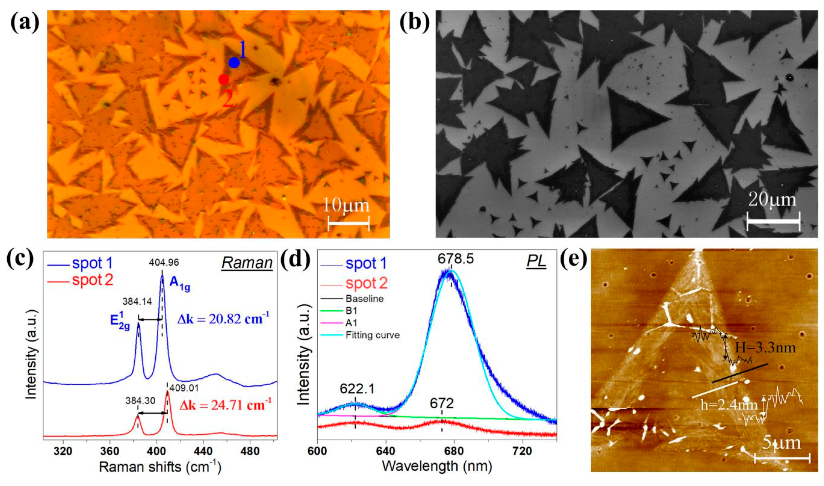
2.3. Characterizations

Optical microscope (OM) images of MoS2 domains were observed using the Nikon Eclipse Ti-U (Nikon, Tokyo, Japan) and Mshot MJ30 (Mshot, Guangzhou, China). Scanning electron microscopy (SEM) images were acquired using a FEI Quanta 450. Raman (FEI Quanta, Hillsboro, OR, USA) and photoluminescence (PL) spectroscopy were performed using a Renishaw inVia Reflex system (Renishaw, Wharton Andech, UK) with a Leica dark-field microscope. The wavelength of the excitation laser was 532 nm, and the focus diameter was approximately 1 μm. The surface feature and film thickness of MoS2 domains were measured by an atomic force microscope (AFM, NTEGRA Spectra, NT-MDT, Moscow, Russia).

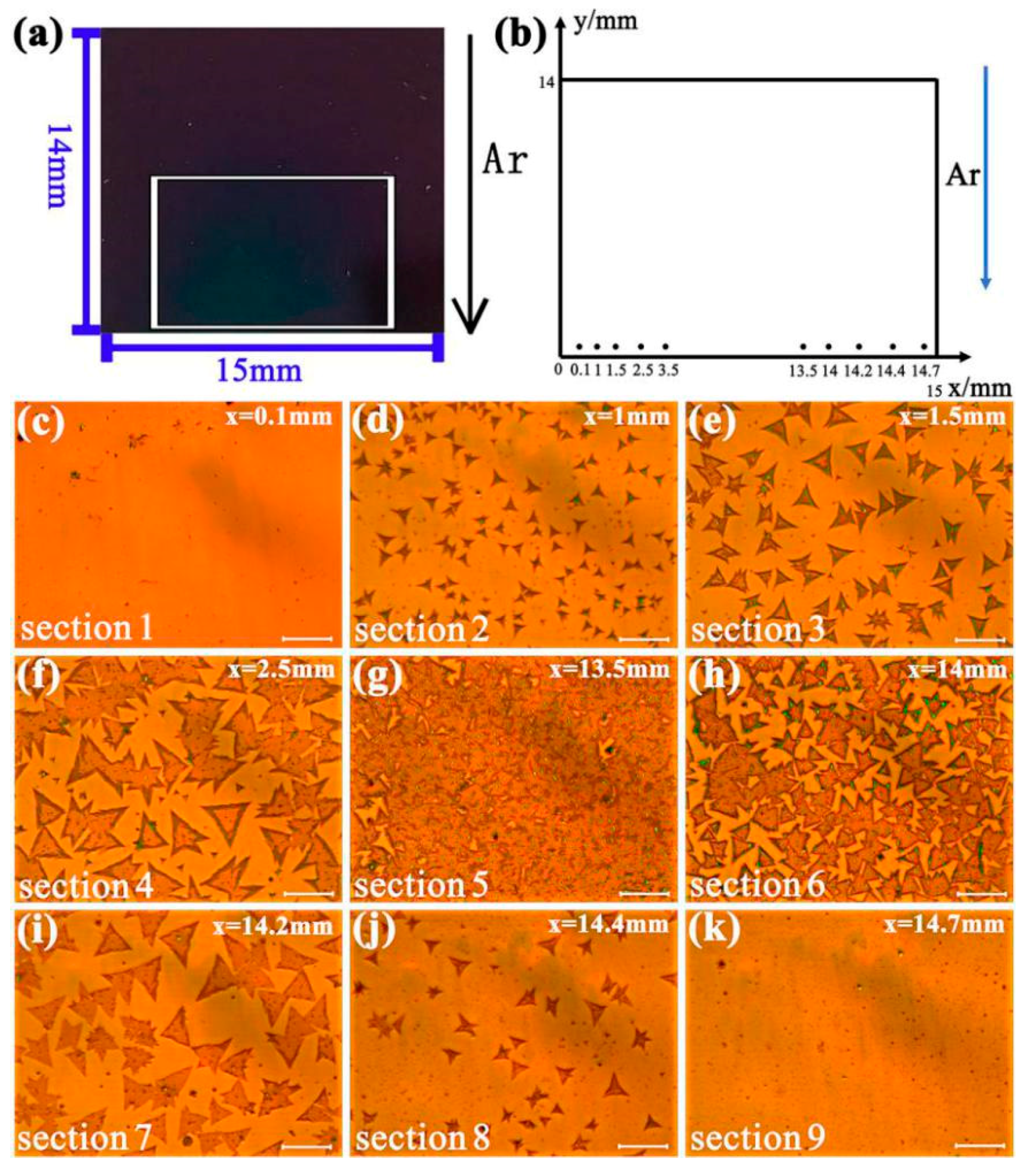
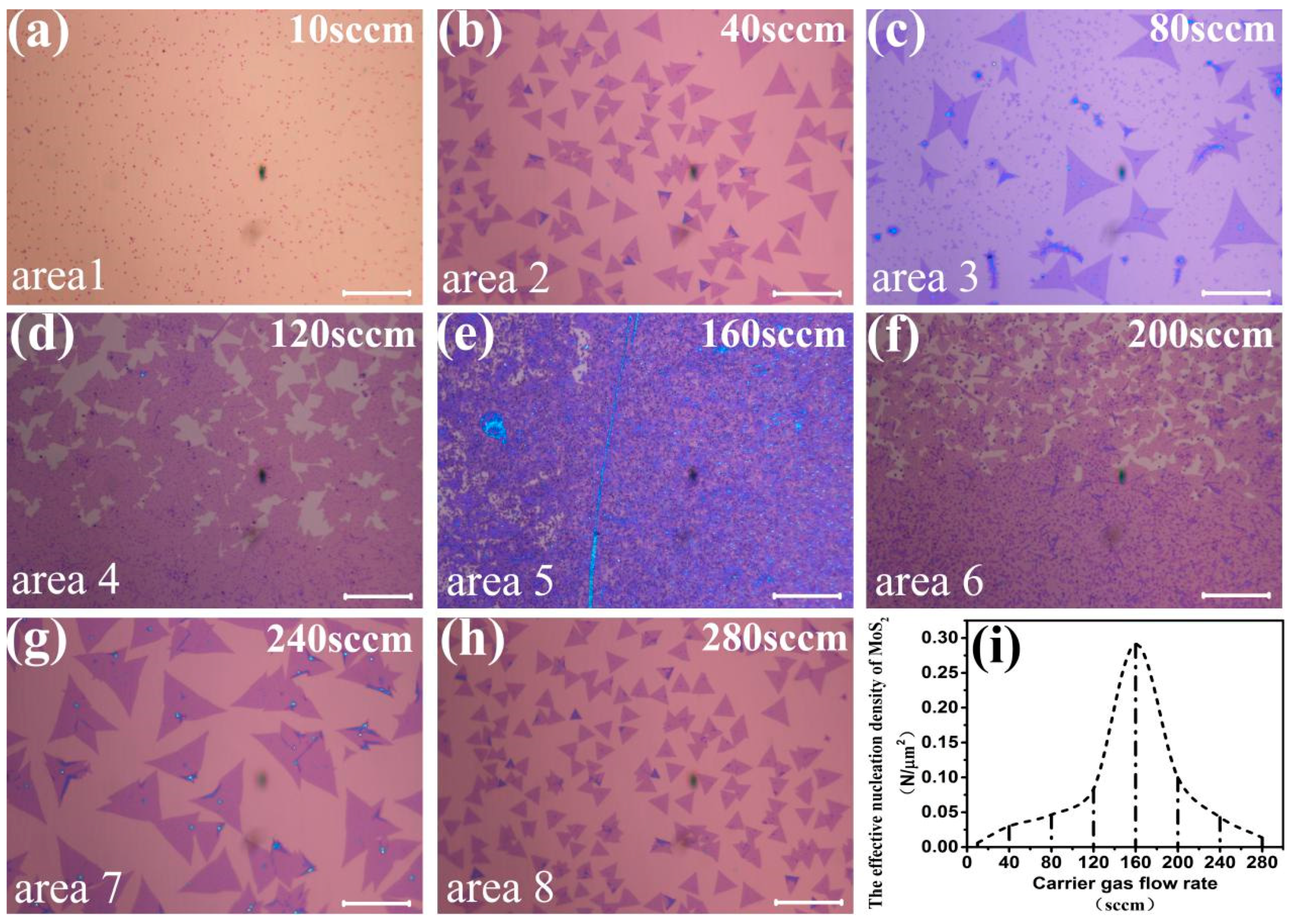
3. Results and Discussion

The crystal features of MoS2 grown on the SiO2/Si substrates were analyzed. As shown in Figure 2a, MoS2 nanosheets are successfully deposited on the SiO2/Si substrate. According to the optical contrast of MoS2 nanosheets [23], the film thickness in the inner position of the sample is relatively thinner than that in the edge position. In order to further investigate the surface morphology of the sample, we used SEM to examine the MoS2 nanosheets. In Figure 2b, we can find a distinct layered effect where the color depth in the edge position of the sample is deeper than that in the internal position. This is similar to the thickness distribution of MoS2 nanosheets observed using OM.
To further confirm the number of layers, we chose two spots in the sample to be characterized by Raman and PL spectroscopy. One spot (blue spot) is in the internal position (region 1) and the other spot (red point) is in the edge position (region 2). It was found that there were two obvious Raman peaks in Figure 2c. E12g represents the in-plane vibrational mode between the molybdenum atom and the sulfur atom. A1g stands for the out-of-plane vibrational mode between sulfur atoms [24]. Δk, the Raman frequency difference between E12g and A1g, can determine the number of layers [25]. The two Raman peaks of the blue spot are located at 384.14 and 404.96 cm−1, so the Δk is 20.82 cm−1. This Δk corresponds to monolayer MoS2 [26]. Similarly, in the red spot, the two Raman peaks are located at 384.30 and 409.01 cm−1, and the Δk is 24.71 cm−1, which corresponds to few-layer MoS2 [15,26]. With the decreased number of layers, the band-gap of MoS2 gradually shifts from the indirect band-gap to the direct band-gap. In terms of Figure 2d, the PL spectra of monolayer MoS2 in the blue spot, we can see two resonant points at 678.5 nm (1.82 eV) and 622 nm (1.99 eV). The two resonant points correspond to A1 (the maximal splitting valence band) and B1 (the minimum conduction band), the direct exciton transition of monolayer MoS2. The PL spectra was fitted with Gaussian curves. The full width at half maximum (FWHM) of peak at 678.5 nm is 30.2 nm and that of 622 nm is 23.8 nm. On the other hand, the PL spectra of few-layer MoS2 in the red spot show weak PL intensity. The A1 peak is at 672 nm (1.84 eV), and the B1 peak is at 622 nm (1.99 eV). Furthermore, we used AFM to measure the thickness of the sample. According to the measurement results shown in Figure 2e, the height (marked with a white line) between the internal position and the edge position of the sample is h = 2.4 nm. The height (labeled with a white line) between the edge position and the substrate is H = 3.3 nm. Thus, the height between the internal position and the substrate is about 0.9 nm, which is consistent with the thickness of monolayer MoS2 [27].
The size and coverage of the MoS2 domains are highly dependent on the distribution of the samples in the spatial location of the substrate [27]. To better observe this phenomenon, we created an XY-coordinate system where the bottom left corner of a substrate (Figure 3a) is taken as the origin O. As shown in Figure 3b, the y-axis is along the airflow and the x-axis is vertical the airflow. In the rectangular coordinate system, at y = 1.0 mm, 10 points were selected on the x-axis (in the direction of vertical airflow) for observation. According to the distribution characteristics of MoS2 domains, nine representative images were selected for display, as shown in Figure 3c–k. At x = 0.1 mm (Figure 3c), owing to the low evaporation concentration of MoO3, only small black nuclei appeared on the SiO2/Si substrate. At x = 1 mm (Figure 3d), the generated MoS2 domain appeared as small triangles and darts discretely. The triangular side of the largest domain reached up to 7 μm. At x = 1.5 mm (Figure 3e), with a larger domain size, regular triangles were formed. The side length of the largest triangular domain is about 15 μm. At x = 2.5 mm (Figure 3f), it is observed that part of MoS2 triangles are connected together to form some irregular film. The largest side of the triangular domain in this area is above 20 μm. Furthermore, large-scale MoS2 film has continuous coverage in the range of x = 3.5 to 13.5 mm (Figure 3g). As depicted in Figure 3h–k, contrary to the distribution in Figure 3c–f, the size of MoS2 samples decreases with the further increase of x. From y = 0 to 6.2 mm, a similar distribution of the MoS2 samples can be found along the x direction.
The differences of MoS2 domains in the direction vertical to the airflow (x-axis) are shown distinctly in the above OM images. Along the x-axis, the shapes of MoS2 were changed in the following order: small nucleated particles, small triangles, larger triangles, then large-sized film. Then, the film size gradually shrunk and became sparser. From Figure 3c–f, it can be inferred that that the vapor concentration of MoS2 increased continuously along the positive direction of the x-axis before MoS2 film formation. In Figure 3d, MoS2 domains would start growing from hexagonal nuclei with three Mo-zz and three S-zz sides. In this area, the Mo:S ratio condition was <1:2 so that small triangles and darts formed. From Figure 3f–h, it can be seen that a sufficient supply of MoS2 vapor results in large triangles and continuous film. In this area, the Mo:S ratio condition was ≥1:2 [27]. After the vapor concentration of MoS2 reached the maximum (i.e., filming phenomenon occurring), the MoS2 layer began to become discontinuous with the growth of the x-axis (Figure 3h–k), presenting a relatively sparse, discrete distribution of triangular MoS2 films. Meanwhile, there was a shrinkage in size and quantity with respect to these triangles. Based on the above analysis, we can deduce that there was an obviously a gradient distribution of MoS2 domain size in a cross-section vertical to the direction of airflow due to the difference of MoS2 vapor concentration.
To explore the size distribution rule of the MoS2 domain on the substrate, we chose five sections, as shown in Figure 3e–i. Each section had the same area (20,164 μm2) and labeled as Sections 1–5. The number of effective nucleation points (i.e., the nucleation points with MoS2 geometric area greater or equal to 0.5 μm2) and the nucleation density (i.e., the number of effective nucleation points per unit area) within the chosen section were statistically measured. According to statistical numbers in Table 1, the highest nucleation density is in Section 3, similar to the optical micrograph in Figure 3g. This area has the largest size of MoS2 film. Thus, the distribution rule of MoS2 domains on the substrate can be summarized as follows. For the same substrate along the direction vertical to the airflow, the nucleation density is related to the distance of the midcourt-line position of the substrate. The size of MoS2 thin film is larger as the distance is closer. Inversely, the larger the distance is, the smaller the size of the MoS2 thin film is and the fewer nucleation density of MoS2 is.
To explain the relationship between the nucleation density of MoS2 and the size distribution of MoS2 domains, we employed the laminar flow theory to analyze the airflow distribution. The largest speed of carrier airflow occurred in the center of the quartz tube, and the speed near the inwall of the quartz tube is close to zero [28,29]. Thus, along the direction vertical to the airflow, the speed of the carrier gas (Ar) is larger at the center surface of substrates than that their side. Since faster carrier gasses can transport more reactants in the same time, the area with a faster carrier gas can form more effective nucleation points, resulting in an increase of the crystal growth size [30]. As depicted in Figure 3g, the nucleation density also increased in the center region of substrates and MoS2 film formed. On the contrary, the area with a slower carrier gas can form less effective nucleation points, resulting in a decrease of nucleation density. As shown in Figure 3g, it is noted that a high nucleation density will increase growth points in the center area. An abundant supply of MoS2 vapor will make isolated MoS2 domains connect together. As shown in Figure 3e,i, when close to the side of the substrates, there is lower nucleation density, and enough MoS2 vapor enables the growth of larger sized triangles in this area. Furthermore, when at the side of the substrates, the lack of nuclei and vapor of MoS2 led to small triangles and discrete darts. Thus, domain morphology is highly dependent on nucleation density [31]. Thus, controlling the speed of carrier gas will be an effective approach for regulating nucleation density. Using this approach can also adjust the formation of MoS2 domains [19,22].
To further explore the influence of carrier gas flow rates on the nucleation density, we prepared MoS2 samples under the same conditions with different carrier gas flow rates, from 10, 40, 80, 120, 160, 200, to 240 sccm. Optical micrographs of MoS2 samples in the center point (x = 7.5 mm, y = 7.0 mm) of substrates with different carrier gas flow rates are shown in Figure 4a–h. The relationship between different carrier gas flow rates and their corresponding nucleation density is shown in Figure 4i. While the gas flow rate was 10 sccm, the nucleation density of MoS2 was 0.0061 N/μm2. Only MoS2 nuclei were found on substrates (Figure 4a). Although low gas flow rates lead to high concentrations of S vapor to fully sulfurize MoO3, it suffers from low transfer efficiency of the MoS2 vapor. As a result, few MoS2 nuclei can be deposited on substrates. By increasing gas flow rates in the range of 0–160 sccm, the concentration of S vapor decreased, but the concentration of MoS2 vapor was still enough. Therefore, the nucleation density of MoS2 increased. Thus, the growth of MoS2 was promoted in low flow rates. While the gas flow rate was 160 sccm, nucleation density reached the top value of 0.2912 N/μm2 and large-scale films of MoS2 were formed (Figure 4e). Even gas flow rates further increased from 160 to 280 sccm. The concentration of S vapor was not enough to maintain reactions of MoS2 synthesizing [32]. Therefore, the nucleation density of MoS2 decreased and the shape of MoS2 domains changed from disconnected film, to large triangles, then to small triangles (Figure 4f–h). Thus, the growth of MoS2 was suppressed in high flow rates. Finally, according to these experiment results, controlling the carrier gas flow rate can also control the shape and coverage of MoS2 domains.

4. Conclusions

In summary, we have shown a simple CVD method to synthesize 2D MoS2 crystals at atmospheric pressure. The results show that the size of MoS2 domains is 10 μm with fast growth. Raman, PL, and AFM measurements demonstrate that the inner region of triangular MoS2 domains were monolayer and the edge region were few-layer. It is observed that the shape of MoS2 domains vary from discrete darts, to triangles, to continuous film on the substrate. We also explore the distribution rule of synthesized MoS2 on SiO2/Si substrate. The nucleation density and the size and shape of MoS2 domains are related to the distance to the midcourt-line position of the substrate along the direction of the airflow. We employed the laminar flow theory to comprehend this distribution rule. It is noted that the changing the speed of the carrier gas at the substrate surface will control the nucleation density and adjust the formation of MoS2 domains. Furthermore, we explore the relationship between the carrier gas flow rate and the nucleation density. The results demonstrate that controlling the carrier gas flow rate will be an effective approach to control the size and coverage of MoS2 domains. It provides a valuable reference to understand the growth regulation of 2D MoS2.

Author Contributions

H.X. and F.L. conceived and designed the experiments. W.Z., X.Z., J.H., X.F., L.Y., and G.X. performed the synthesis experiments. W.Z., J.H., and L.Y. analyzed the data. H.X. and F.L. contributed reagents and analysis tools. H.X., and W.Z. wrote the paper.

Funding

This work has been supported by the following research program. F.L. acknowledges financial support from the National Science Foundation of China (Grant No. 61571197 and 61172011), the Guangdong Natural Science Foundation (Grant No. 10151064201000006), and the Visiting Scholars Fund of the State Key Laboratory of Silicon Materials (Grant No. SKL2014-5).

Conflicts of Interest

The authors declare no conflict of interest.

References

  1. Liu, L.; Liu, Z.; Huang, P.; Wu, Z.; Jiang, S. Protein-induced ultrathin molybdenum disulfide (MoS2) flakes for a water-based lubricating system. RSC Adv. 2016, 6. [Google Scholar] [CrossRef]
  2. Zhan, Y.; Liu, Z.; Najmaei, S.; Ajayan, P.M.; Lou, J. Large Area Vapor Phase Growth and Characterization of MoS2 Atomic Layers on SiO2 Substrate. Small 2012, 8, 966. [Google Scholar] [CrossRef] [PubMed]
  3. Island, J.O.; MolinaMendoza, A.J.; Barawi, M.; Biele, R.; Flores, E.; Clamagirand, J.M.; Ares, J.R.; Sanchez, C.; van der Zant, H.S.J.; D’Agosta, R.; et al. Electronics and optoelectronics of quasi-one dimensional layered transition metal trichalcogenides. 2D Mater. 2017, 4. [Google Scholar] [CrossRef]
  4. Amani, M.; Chin, M.L.; Birdwell, A.G.; O’Regan, T.P.; Najmaei, S.; Liu, Z.; Ajayan, P.M.; Lou, J.; Dubey, M. Electrical performance of monolayer MoS2 field-effect transistors prepared by chemical vapor deposition. Appl. Phys. Lett. 2013, 102, 136805. [Google Scholar] [CrossRef] [Green Version]
  5. Lee, H.S.; Kim, M.S.; Jin, Y.; Han, G.H.; Lee, Y.H.; Kim, J. Efficient Exciton–Plasmon Conversion in Ag Nanowire/Monolayer MoS2 Hybrids: Direct Imaging and Quantitative Estimation of Plasmon Coupling and Propagation. Adv. Opt. Mater. 2015, 3, 943–947. [Google Scholar] [CrossRef]
  6. Radisavljevic, B.; Radenovic, A.; Brivio, J.; Giacometti, V.; Kis, A. Single-layer MoS2 transistors. Nat. Nanotechnol. 2011, 6, 147–150. [Google Scholar] [CrossRef] [PubMed]
  7. Cho, K.; Pak, J.; Kim, J.K.; Kang, K.; Kim, T.Y.; Shin, J.; Choi, B.Y.; Chung, S.; Lee, T. Contact-Engineered Electrical Properties of MoS2 Field-Effect Transistors via Selectively Deposited Thiol-Molecules. Adv. Mater. 2018, e1705540. [Google Scholar] [CrossRef] [PubMed]
  8. Zhang, W.; Huang, J.K.; Chen, C.H.; Chang, Y.H.; Cheng, Y.J.; Li, L.J. High-Gain Phototransistors Based on a CVD MoS2 Monolayer. Adv. Mater. 2013, 25, 3456–3461. [Google Scholar] [CrossRef] [PubMed]
  9. Xu, H.; Han, X.; Dai, X.; Liu, W.; Wu, J.; Zhu, J.; Kim, D.; Zou, G.; Sablon, K.A.; Sergeev, A.; et al. High Detectivity and Transparent Few-Layer MoS2/Glassy-Graphene Heterostructure Photodetectors. Adv. Mater. 2018, 30, e1706561. [Google Scholar] [CrossRef] [PubMed]
  10. Sundaram, R.S.; Engel, M.; Lombardo, A.; Krupke, R.; Ferrari, A.C.; Avouris, P.; Steiner, M. Electroluminescence in single layer MoS2. Nano Lett. 2013, 13, 1416. [Google Scholar] [CrossRef] [PubMed]
  11. Choi, G.J.; Van, L.Q.; Choi, K.S.; Kwon, K.C.; Jang, H.W.; Gwag, J.S.; Kim, S.Y. Polarized Light-Emitting Diodes Based on Patterned MoS2 Nanosheet Hole Transport Layer. Adv. Mater. 2017, 29, 1702598. [Google Scholar] [CrossRef] [PubMed]
  12. Tsai, M.L.; Su, S.H.; Chang, J.K.; Tsai, D.S.; Chen, C.H.; Wu, C.I.; Li, L.J.; Chen, L.J.; He, J.H. Monolayer MoS2 heterojunction solar cells. ACS Nano 2014, 8, 8317–8322. [Google Scholar] [CrossRef] [PubMed]
  13. Singh, E.; Kim, K.S.; Yeom, G.Y.; Nalwa, H.S. Atomically Thin-Layered Molybdenum Disulfide (MoS2) for Bulk-Heterojunction Solar Cells. ACS Appl. Mater. Interfaces 2017, 9, 3223. [Google Scholar] [CrossRef] [PubMed]
  14. Li, H.; Yin, Z.; He, Q.; Li, H.; Huang, X.; Lu, G.; Fam, D.W.H.; Tok, A.I.Y.; Zhang, Q.; Zhang, H. Layered Nanomaterials: Fabrication of Single-and Multilayer MoS2 Film-Based Field-Effect Transistors for Sensing NO at Room Temperature (Small 1/2012). Small 2012, 8, 2. [Google Scholar] [CrossRef]
  15. Zheng, J.; Yan, X.; Lu, Z.; Qiu, H.; Xu, G.; Zhou, X.; Wang, P.; Pan, X.; Liu, K.; Jiao, L. High-Mobility Multilayered MoS2 Flakes with Low Contact Resistance Grown by Chemical Vapor Deposition. Adv. Mater. 2017, 29, 1604540. [Google Scholar] [CrossRef] [PubMed]
  16. Li, X.L.; Prof, Y.D.L. Formation of MoS2 Inorganic Fullerenes (IFs) by the Reaction of MoO3 Nanobelts and S. Chem. Eur. J. 2003, 9, 2726–2731. [Google Scholar] [CrossRef] [PubMed]
  17. Lee, Y.H.; Yu, L.; Wang, H.; Fang, W.; Ling, X.; Shi, Y.; Lin, C.T.; Huang, J.K.; Chang, M.T.; Chang, C.S.; et al. Synthesis and Transfer of Single-Layer Transition Metal Disulfides on Diverse Surfaces. Nano Lett. 2013, 13, 1852. [Google Scholar] [CrossRef] [PubMed]
  18. Gong, C.; Huang, C.; Miller, J.; Cheng, L.; Hao, Y.; Cobden, D.; Kim, J.; Ruoff, R.S.; Wallace, R.M.; Cho, K.; et al. Metal Contacts on Physical Vapor Deposited Monolayer MoS2. ACS Nano 2013, 7, 11350–11357. [Google Scholar] [CrossRef] [PubMed]
  19. Wang, S.; Pacios, M.; Bhaskaran, H.; Warner, J.H. Substrate control for large area continuous films of monolayer MoS2 by atmospheric pressure chemical vapor deposition. Nanotechnology 2016, 27, 085604. [Google Scholar] [CrossRef] [PubMed]
  20. Ling, X.; Lee, Y.H.; Lin, Y.; Fang, W.; Yu, L.; Dresselhaus, M.S.; Kong, J. Role of the Seeding Promoter in MoS2 Growth by Chemical Vapor Deposition. Nano Lett. 2014, 14, 464. [Google Scholar] [CrossRef] [PubMed]
  21. Njiwa, P.; Aurélie, H.A.; Afanasiev, P.; Geantet, C.; Bosselet, F.; Vacher, B.; Thierry Le Mogne, M.B.; Dassenoy, F. Tribological Properties of New MoS2, Nanoparticles Prepared by Seed-Assisted Solution Technique. Tribol. Lett. 2014, 55, 473–481. [Google Scholar] [CrossRef]
  22. Kim, H.; Ovchinnikov, D.; Deiana, D.; Unuchek, D.; Kis, A. Suppressing nucleation in metalorganic chemical vapor deposition of MoS2 monolayers by alkali metal halides. Nano Lett. 2017. [Google Scholar] [CrossRef] [PubMed]
  23. Late, D.J.; Liu, B.; Matte, H.S.S.R.; Rao, C.N.R.; Dravid, V.P. Rapid Characterization of Ultrathin Layers of Chalcogenides on SiO2/Si Substrates. Adv. Funct. Mater. 2012, 22, 1894–1905. [Google Scholar] [CrossRef]
  24. Splendiani, A.; Sun, L.; Zhang, Y.; Li, T.; Kim, J.; Chim, C.Y.; Galli, G.; Wang, F. Emerging Photoluminescence in Monolayer MoS2. Nano Lett. 2010, 10, 1271–1275. [Google Scholar] [CrossRef] [PubMed]
  25. Lee, Y.H.; Zhang, X.Q.; Zhang, W.; Chang, M.T.; Lin, C.T.; Chang, K.D.; Yu, Y.C.; Wang, J.T.; Chang, C.S.; Li, L.J.; et al. Synthesis of large-area MoS2 atomic layers with chemical vapor deposition. Adv. Mater. 2012, 24, 2320–2325. [Google Scholar] [CrossRef] [PubMed]
  26. Yu, Y.; Li, C.; Liu, Y.; Su, L.; Zhang, Y.; Cao, L. Controlled scalable synthesis of uniform, high-quality monolayer and few-layer MoS2 films. J. Sci. Rep. 2013, 3, 1866. [Google Scholar] [CrossRef] [PubMed]
  27. Wang, S.; Rong, Y.; Fan, Y.; Pacios, M.; Bhaskaran, H.; He, K.; Warner, J.H. Shape Evolution of Monolayer MoS2 Crystals Grown by Chemical Vapor Deposition. Chem. Mater. 2014, 26. [Google Scholar] [CrossRef]
  28. Govind, R.A.; Warner, J.H.; Blankschtein, D.; Strano, M.S.A. Generalized Mechanistic Model for the Chemical Vapor Deposition of 2D Transition Metal Dichalcogenide Monolayers. ACS Nano 2016, 10, 4330. [Google Scholar] [CrossRef] [PubMed]
  29. Incropera, F.P. Fundamentals of Heat and Mass Transfer; John Wiley & Sons: Hoboken, NJ, USA, 2007. [Google Scholar]
  30. Stoica, T.; Stoica, M.; Duchamp, M.; Tiedemann, A.; Mantl, S.; Grützmacher, D.; Buca, D.; Kardynał, B.E. Vapor transport growth of MoS2, nucleated on SiO2, patterns and graphene flakes. Nano Res. 2016, 9, 3504–3514. [Google Scholar] [CrossRef]
  31. Chen, B.; Yu, Q.; Yang, Q.; Bao, P.; Zhang, W.; Lou, L.; Zhu, W.; Wang, G. Large-area high quality MoS2 monolayers grown by sulfur vapor counter flow diffusion. RSC Adv. 2016, 6, 50306–50314. [Google Scholar] [CrossRef]
  32. Cao, Y.; Luo, X.; Han, S.; Yuan, C.; Yang, Y.; Li, Q.; Yu, T.; Ye, S. Influences of carrier gas flow rate on the morphologies of MoS2, flakes. Chem. Phys. Lett. 2015, 631, 30–33. [Google Scholar] [CrossRef]
Figure 1. (a) Schematic of the CVD (chemical vapor deposition) experimental device. (b)Temperature control process of MoO3 and S in the CVD system.
Materials 11 00870 g001
Figure 2. (a) Optical images for the MoS2 sample. (b) SEM (Scanning electron microscopy) images of the MoS2 sample. (c) The Raman spectroscopy images of the colored circular points corresponding to the areas marked 1 and 2 in (a). The laser wavelength was 532 nm. (d) The photoluminescence spectroscopy image of the colored circular points corresponding to the two areas marked 1 and 2 in (a). The laser wavelength was 532 nm. (e) An AFM (atomic force microscope) image of the triangle MoS2 sample. The height between the internal position and the edge position of the product (white measurement line, marked h) is 2.4 nm, and the height between the edge position and the SiO2/Si substrate (black measuring line, marked H) is 3.3 nm.
Materials 11 00870 g002
Figure 3. (a) Image of the deposition of MoS2 on the SiO2/Si substrates. (b) The Cartesian coordinate map of the selected nine MoS2 sample growth regions (ck) in (a). (ck) The optical image of MoS2 samples in different growth areas. Scale bar: 20 μm.
Materials 11 00870 g003
Figure 4. Effects of different carry gas flow rate on the effective nucleation density of MoS2. (ah) MoS2 optical microscopy images of samples grown on the SiO2/Si substrates with different gas flow rates: 10, 40, 80, 120, 160, 200, 240, and 280 sccm. Scale bar: 20 μm. (i) The relationship diagram between the different carry gas flow rates (ah) and the corresponding nucleation density of MoS2.
Materials 11 00870 g004
Table 1. A comparison of the number of effective nucleation points and the effective nucleation density of MoS2 in the same area of different regions.
SectionThe Number of Effective Nucleation Points of MoS2 (N)The Effective Nucleation Density of MoS2 (N/μm2)
Section 1 (Figure 3e)2070.0103
Section 2 (Figure 3f)3360.0167
Section 3 (Figure 3g)7840.0389
Section 4 (Figure 3h)6080.0302
Section 5 (Figure 3i)720.0036

