
Ultrafast Laser Additive Manufacturing: A Review


1
Department of Engineering Physics, McMaster University, Hamilton, ON L8S 4L8, Canada
2
Department of Mechanical Engineering, McMaster University, Hamilton, ON L8S 4L8, Canada
*
Author to whom correspondence should be addressed.
J. Manuf. Mater. Process. 2023, 7(3), 89; https://doi.org/10.3390/jmmp7030089
Submission received: 12 March 2023
/
Revised: 9 April 2023
/
Accepted: 13 April 2023
/
Published: 5 May 2023
(This article belongs to the Special Issue Editorial Board Members’ Collection Series: Additive Manufacturing)
Abstract
:Ultrafast lasers are proven and continually evolving manufacturing tools. Concurrently, additive manufacturing (AM) has emerged as a key area of interest for 3D fabrication of objects with arbitrary geometries. Use of ultrafast lasers for AM presents possibilities for next generation manufacturing techniques for hard-to-process materials, transparent materials, and micro- and nano-manufacturing. Of particular interest are selective laser melting/sintering (SLM/SLS), multiphoton lithography (MPL), laser-induced forward transfer (LIFT), pulsed laser deposition (PLD), and welding. The development, applications, and recent advancements of these technologies are described in this review as an overview and delineation of the burgeoning ultrafast laser AM field. As they mature, their adoption by industry and incorporation into commercial systems will be facilitated by process advancements such as: process monitoring and control, increased throughput, and their integration into hybrid manufacturing systems. Recent progress regarding these aspects is also reviewed.
1. Introduction
Additive manufacturing (AM) is a production process where an object is constructed by joining materials together, typically in a layer-by-layer fashion and often from a three-dimensional computer-aided design (CAD) model. AM offers many benefits, such as the ability to produce true internal geometries, on-demand customized parts, freedom to design complex parts, and reduced environmental impact [1,2,3,4]. Consequently, the field has grown at a rapid pace. An area of AM that has drawn significant attention is that of laser-based AM. Lasers are an indispensable manufacturing tool because they are well-controlled in space via focusing elements, spatial light modulators, etc., and are well-controlled in time by their pulse duration and repetition rate.
Ultrafast lasers are valuable research and manufacturing tools. The ultrashort pulse duration is comparable to electron-lattice relaxation times, yielding unique interactions with matter, particularly nonlinear absorption, melting, and ablation. A common application of ultrafast lasers is subtractive manufacturing, wherein materials such as metals and dielectrics are ablated, cut, or otherwise modified. As a well-established tool for high-precision manufacturing and material modification, ultrafast ablation can be combined with other burgeoning additive manufacturing methods, such as powder-bed fusion, to provide further control over build morphology [5]. The utility of these lasers is not limited to post-processing ablation, however, as they offer great potential as the additive manufacturing tool itself. Over the past few decades, several techniques capitalizing on the unique abilities of ultrafast lasers have been developed. These are: multiphoton lithography (MPL), laser-induced forward transfer (LIFT), selective laser melting/sintering (SLM/SLS), pulsed laser deposition (PLD), and welding. MPL is the most established, as signified by the availability of commercial systems. The applications of ultrashort pulse lasers in additive manufacturing aim to fill gaps left by conventional techniques, especially on the nano- and micro-scale. Both additive and subtractive manufacturing are accomplished with ultrafast lasers, which presents the possibility of hybrid, all-in-one devices using a single laser source. While techniques such as MPL and LIFT have been reviewed, a comprehensive review of ultrafast laser additive manufacturing techniques and process advancements has not been provided. It is the intention of this review to provide an overview of the state of the art, and in doing so provide the reader with a jumping-off point to delve further into these topics. Furthermore, the landscape for ultrafast laser technology is rapidly changing. Relatively low-cost fiber systems decrease the barrier of entry while delivering high repetition rates more useful for commercial and industrial applications. As these areas of research are growing, this review delineates ultrafast laser additive manufacturing as a field of its own, laying the groundwork for future discussions of progress and challenges in the field.
2. Brief Description of Ultrafast Lasers
Since the first report of laser action in 1960, lasers have undergone significant advancement and played a crucial role in many seminal discoveries and publications [6]. Lasers can be operated in a continuous wave (CW) mode, in which their output intensity is constant over time, or they can be pulsed. Two essential ways for pulsing a laser are Q-switching and mode locking. Q-switching was first demonstrated with a ruby laser and Kerr cell shutters in 1961 [7]. Although conventional Q-switching produces nanosecond pulses, they have difficulties producing pulses of picosecond duration due to large cavity lengths [8,9,10]. To generate the ultrashort pulses of interest, down to single-digit femtosecond durations, mode locking is the universal technique [11]. First observed in a HeNe laser in 1964 [12], mode locking was achieved in dye and rare-earth doped solid-state lasers (e.g., Nd3+, Er3+, Yb3+). In 1986, a new high-gain cross section, broad absorption and emission linewidths, solid-state lasing medium came onto the scene: titanium-doped sapphire (Ti:Al2O3) [13]. Ti:Sapphire lasers combine advantages from both dye and rare-earth doped lasers and were a promising candidate for a more practical femtosecond laser. Indeed, Spence et al. [14] discovered self-mode-locking in a Ti:Sapphire laser due to the Kerr-lens mode-locking (KLM) effect. This effect, in addition to other improvements, such as dispersion compensation methods and the introduction of semiconductor saturable absorber mirrors (SESAMs), allows for the reliable generation of pulses as short as 6.5 fs [15]. As a practical and tunable femtosecond source, Ti:Sapphire lasers are responsible for significant advancement in scientific understanding of the behavior of physical systems at these timescales, spectroscopy, nonlinear optics, and with increased amplification, material processing and manufacturing [16].
Parallel to the emergence of Ti:Sapphire lasers, mode-locked Nd-doped fiber lasers generating ultrashort pulses were developed [17,18]. While much of the interest has been in communications and data transmission applications, fiber architectures also allow for pulse energies that enable machining and manufacturing. Commercial ultrashort Er-fiber (1.55 µm) and Yb-fiber (1.03 µm) lasers are now prevalent, and are more adaptable, compact, and require less alignment than their rod-shaped counterparts [19]. For industrial applications, their high average power and repetition rates (tens of MHz) are attractive for efficient material processing. There are many recent reviews on ultrafast fiber lasers, such as [19,20,21].
Amplification of ultrashort pulses is a challenge due to the high peak power and the nonlinear optical effects it can produce in air and gain media, leading to plasma formation and damage [22]. Strickland et al. [23] introduced a method of amplification, referred to as chirped pulse amplification, in which the pulses are stretched to reduce the peak intensity, amplified in a gain medium while remaining below the damage threshold, and then compressed in the opposite manner of the stretching so that the ultrashort pulse is recovered with peak intensities in the TW regime. The resultant setup for most high-power, ultrashort laser systems, is that of the master oscillator power amplifier (MOPA) design. The master oscillator is a mode-locked laser that is optimized for pulse duration, center wavelength, and spatial beam qualities. The (comparatively) low-energy pulses are passed into power amplifiers for high power pulses. Commercial ultrafast systems commonly provide > 1 W average power and mJ pulse energies. Such pulses are sufficiently powerful to initiate unique interactions with many materials that lead to manufacturing techniques, such as nanoscale and micron scale ablation, multiphoton polymerization, laser-induced forward transfer, pulsed laser deposition, and others.
3. Ultrashort Pulse Laser-Matter Interaction
The unique interactions between ultrashort laser pulses and matter can be explained by the pulse duration and intensity. For material modification purposes, focused beams deliver high peak intensities (~1015 W/cm2) over a period that is shorter than or comparable to the heat and energy transfer processes between the electron and lattice subsystems [24,25]. Highly localized nonlinear absorption occurs, causing extreme energy gradients and rapid heating (1014 K/s) and cooling rates that result in melting, ablation, and/or complex structural and phase changes (Figure 1) [26,27,28,29,30,31].
3.1. Metals and the Two-Temperature Model
In strongly absorbent materials such as metals, ultrashort pulse radiation is absorbed by conduction-band electrons via inverse Bremsstrahlung. Electron subsystem thermalization is on the order of femtoseconds, and the electrons transfer their energy to atomic lattice vibrations (electron-phonon coupling) picoseconds after irradiation [28]. Since the pulse duration is shorter than the electron–lattice equilibration time, the nonequilibrium situation is described by a two-temperature model wherein the time evolution of electron and ion temperatures are treated separately and connected by an electron–lattice coupling constant [32,33,34]. The two-temperature model equations state:
where e and l refer to electron and lattice parameters, C the heat capacity, k the thermal diffusivity, Γ the electron-lattice coupling constant, and Q the irradiating laser.
If the intensity is high enough, the transfer of energy from the superheated electrons into the lattice subsystem results in a violent phase change and material ejection with micro- to nano-meter resolution [35,36,37]. Since thermal diffusion into the bulk material occurs on a longer timescale, the surrounding material heats less appreciably. Thus, the heat-affected zone of ultrafast laser modification is significantly smaller than that of ns or continuous wave lasers, producing minimal collateral damage and making it desirable for micro- and nano-machining applications. If the fluence is below the ablation threshold, there are melting regimes in which the nonequilibrium situation rapidly heats the lattice to the melting point. For sufficiently high intensities, superheating of the lattice gives way to homogeneous nucleation and melting mere picoseconds after the pulse [38,39,40].
3.2. Bandgap Materials
In bandgap materials, electrons are first excited into the conduction band and then continue to absorb photons and increase in energy. For longer pulses, these electrons transfer energy to the lattice and cause subsequent heating and damage [41]. The electronic excitation by high-intensity ultrashort pulses that promotes a significant portion of electrons from the valence band (about 10%) may affect the interatomic bonding, such that melting or other phase transformations occur [42,43]. Such transformations are considered athermal, as they are not a result of lattice equilibration and heating. From the conduction band, free electrons gain kinetic energy by absorbing additional photons, leading to a plasma state, or in the case of extreme ionization, Coulombic explosion [31,44,45].
In the case of wide band gap materials, in which the photon energy is less than the energy needed for excitation into the conduction band, the main processes for ionization are multiphoton, tunneling, and avalanche ionization [46]. A nonlinear optical process, multiphoton absorption is the simultaneous absorption of two or more photons by an electron. This strongly intensity-dependent phenomenon allows ionization if the combined energy is greater than the bandgap. The immense peak intensities of ultrashort pulse lasers readily induce these events. Electrons can also be promoted by tunneling ionization, a phenomenon initially described by Keldysh [47] for dielectrics in strong electromagnetic fields. For high-intensity fields, a qualification often met by ultrashort laser pulses, the Coulomb potential barrier is distorted, making tunnel ionization easier. Under varying laser parameters and material properties, tunneling ionization transitions to multiphoton ionization, and thus both are part of the theoretical treatment in [47]. Conduction band electrons undergo free carrier absorption, attaining higher energy states. If the electrons are further excited by the equivalent of an additional bandgap energy, they can knock other electrons from the valence band to the conduction band, generating additional free carriers [48]. In the presence of sufficient and sustained electromagnetic field strength, newly promoted free carriers undergo the same impact ionization process, giving rise to an ionization “avalanche” [49]. Multiphoton and tunneling ionization produce the seed electrons for the avalanche process [41]. These phenomena facilitate micromachining inside of transparent materials since the light intensity is only sufficient for multiphoton ionization at the laser focal spot [50]. In fact, the pulse energy can be controlled such that only a small portion of the focal spot surpasses the transformation threshold to create sub-wavelength features [51].
3.3. Ultrashort Pulse Ablation
Ultrafast lasers are well known for their use in precision ablation and micromachining. Virtually any material can be ablated by ultrafast lasers, with applications in, but not limited to, metal [52], semiconductor [53], dielectric [54], and bone [55] micromachining, thin film machining [56], microfluidic structure fabrication [57], microelectromechanical systems (MEMS) device manufacturing [58], laser-induced breakdown spectroscopy (LIBS) [59], and implant modification [60]. There are many ablation mechanisms that have been proposed, and they occur under different irradiation parameters and in different materials, as often modelled by hydrodynamic and molecular dynamics simulations [61,62]. Ablation mechanisms include photomechanical spallation, phase explosion, and Coulomb explosion [28,44,45,62,63,64,65,66].
4. Ultrafast Laser Techniques in Additive Manufacturing
4.1. Selective Laser Melting/Sintering
Continuous mode or nanosecond pulse laser-based AM enables direct transfer of energy to a material in a small focal region and leads to curing, sintering, or melting with a better resolution compared to extrusion-based methods [67]. Prominent examples of these methods are selective laser melting (SLM) and selective laser sintering (SLS) (Figure 2). Metals that are commonly used are stainless and tool steels, aluminum alloys, titanium and its alloys, nickel alloys, and some cobalt alloys [68]. Optimal part orientation, laser parameter optimization and consistency, high residual stresses, and surface quality are just some of the challenges within powder-bed fusion processes [69,70]. Managing these challenges for a wide variety of metals with different melting points, laser absorption spectra, and heat conductivity behaviors further complicates the technology. Ultrafast lasers offer possible solutions in the selective laser melting/sintering of hard-to-process materials. Ultrashort pulses deliver intense peak energies on such short timescales that target materials are rapidly heated beyond their melting point but with a small heat-affected zone. Materials with high melting points and/or excellent heat conducting properties may be more easily processed by this confined, extreme heating. Residual heat diffuses rapidly into the bulk due to the short interaction times, but by increasing the pulse repetition rate to the MHz regime, the resulting thermal accumulation can provide additional control of the melting process. Since the heat-affected zone is not much larger than the focal spot diameter, powder particle sizes are restricted to being no larger than the spot size. It should be noted that in general, the melting dynamics of metals under ultrafast laser irradiation are not adequately understood. The thermodynamics of ultrafast laser powder-bed fusion and their influence on material properties are even less so. Thus, the current state of the art is that research is limited primarily to feasibility studies.
4.1.1. Copper
Pure copper is a relatively stable and ductile material with excellent thermal and electrical conductivity [71]. Additive manufacturing of copper is especially attractive because it enables the production of complex geometries that may improve heat transfer devices and does not require additional manufacturing steps like welding [72,73]. The laser processability of copper is limited primarily by its most useful property: high thermal conductivity. Copper absorbs laser energy and dissipates it via significant local thermal gradients, increasing the energy needed to achieve melting and increasing the risk of defects, such as porosity, delamination, and layer curling [74,75,76]. Additionally, high reflectivity results in a compounded need for greater laser power and risks damage to optical components [75,77]. Attempts at selective laser melting of copper via ultrafast lasers are shown in Figure 3. Thin-wall microstructures (<100 µm) with a high porosity were fabricated in [78]. A 1030 nm laser parameter process window was identified at a repetition rate of 20 MHz and pulse energy from 0.75–1.50 µJ, below which superficial sintering occurs and above which ablation occurs. Fully dense structures may require an increased focal spot size and reduced grain size. Density is enhanced in the first several layers by using a steel building platform with a significantly lower thermal conductivity. After approximately 10 layers, the benefits of the steel platform were reduced, and the porous structure emerged (Figure 3c). Further increases in laser power and repetition rate could improve heat accumulation and result in more dense structures. In these experiments, however, with a filling factor of 64% and specific heat and electrical conductivity 10% of that found in literature [79], further progress is necessary for the methods to be viable.
For 2D printable and flexible electronic devices, Cu patterning via the laser sintering of nanoparticles has been investigated [80]. Femtosecond lasers may address challenges posed by copper’s material properties by sintering of Cu nanoparticle ink [81]. A similar process that instead reduces CuO by laser irradiation can produce microstructures on glass and flexible polydimethylsiloxane (PDMS) [82,83]. This was achieved with a lower average power compared to CW and nanosecond lasers; but is hampered by higher oxide concentrations in the patterns [84]. Although Cu nanoparticle sintering average power requirements for femtosecond lasers are lower than CW, evidence shows it results in a smaller processing window that makes consistent quality difficult to achieve [85,86].
4.1.2. Tungsten
Tungsten, also known as wolfram, is a rare metal with a high melting point of 3695 K (for comparison, aluminum melts at 933 K), good thermal conductivity (174 W/m K), and has potential for use in extreme environments, such as nuclear fusion reactors [87]. Consequently, its processability is challenging. In an effort to reduce manufacturing cost and waste, Ref. [88] manufactured Tungsten tiles by directed energy deposition with a non-ultrashort pulse, >3000 W source. The layers deposited were relatively thick (about 1 mm) and suffered from cracks and pores. Conventional SLM has been accomplished with lower laser powers (around 400 W) and with possibly reduced microcrack formation by substrate preheating up to 1000 C [89]. It is thought that the ductile to brittle transformation and large thermal gradients imposed by laser beam melting are responsible for crack formations [90]. Ultrafast lasers may be a more practical and effective source for additively manufacturing Tungsten, as the intense peak power is simulated to produce localized temperatures exceeding 4000 K [32]. Femtosecond selective laser melting is feasible, as shown in [91]. A 0.5 mJ (45 W average power) Yb-fiber laser, with 400 fs pulse width operating at 1 MHz, was used to successively melt more than 100 layers of 1–5 micron powder. Ultimate tensile strength (UTS) and Vickers hardness were measured at 388.4 MPa and 395, respectively. The UTS is greater than conventionally sintered parts around 125 MPa, but lower than polycrystalline tungsten rods which is >580 MPa. Similarly, the Vickers hardness for polycrystalline tungsten is 450. Bai et al. [92] compared pulse durations between 750 fs and CW mode. They found that the fs-based process produced parts with up to 99% density, and fewer defects and greater hardness compared to the ps and CW modes. The reduced incidence of cracks and defects is attributable to higher heating and cooling rates from the ultrafast melting process, which also produces smaller grain sizes leading to the increased hardness. Micron-scale structures were also shown, featuring walls of 100 µm thickness, and a finer microstructure was detected (Figure 4). However, defects are still clearly visible with the ultrafast process. Further testing of material properties (e.g., ductility, dimensional accuracy) will be important to distinguish the ultrafast laser method as an improvement relative to conventional SLM, as well as its capability in demanding applications. As a relatively unexplored technique for SLM, layer-wise ultrashort pulse fabrication is a potential avenue for 3D manufacturing of Tungsten.
4.1.3. Other Materials
Attempts at additively manufacturing a variety of other materials by ultrashort pulses have been made. Ultrafast lasers provide the potential to both heat target materials to extreme temperatures and greatly limit the heat-affected region. Therefore, it is interesting to study how they perform when faced with the challenges of high melting point or low absorption materials as well as the differences in material properties, such as thermal conductivity, melting point, thermal expansion coefficient, etc., at play when dissimilar materials are irradiated simultaneously. Ultrashort pulse laser powder-bed fusion of borosilicate glass [93], aluminum alloys [94,95], ultra-high molecular weight polyethylene (UHMWPE) [96], bimetallics [97], rhenium, and diboride ceramics [98] has been demonstrated. Depending on the investigated material, laser parameters are varied, such that as close to complete melting as possible is achieved (Table 1). Defects and high porosity due to lack of complete melting are a key issue in ultrafast AM parts. Thus, in feasibility studies on melting and additive construction, viable laser parameters are at the core of the investigation. A few examples are shown in Figure 5 [93,94,99].
4.2. Multiphoton Lithography
Stereolithography, a manufacturing process by which light induces a photochemical structural change to print patterns and objects, allows for layer-wise production of arbitrary 3D objects from computer drawn designs. Conventionally, a photopolymer is transformed from the liquid state to a solid polymeric state by UV laser curing [100]. The excitation of a photo-initiator to a state that produces ionic or radical species initiates cross-linking chain reactions in photoresist materials like epoxies and acrylates. Excitation, and thus photopolymerization, can be achieved by multiphoton absorption of lesser energy photons that equates to the energy that would normally be absorbed by singular UV photons. Due to the nonlinear dependence on laser intensity and the transparency of the material to single photon absorption, multiphoton absorption occurs in a tight focal region for ultrafast lasers, meaning that higher resolution and internal modification is accomplished (Figure 6) [101]. Direct laser writing by multi-photon absorption has been discussed in several reviews [101,102,103,104].
The multiphoton lithography technique (also referred to as 3D laser lithography (3DLL) or multiphoton direct laser writing (MP-DLW)) typically utilizes frequency-doubled Ti:Sapphire femtosecond lasers, but as second harmonic fiber lasers have become more viable, they are increasingly common [105]. A variety of materials are available for two-photon polymerization, such as organically modified ceramics (Ormocers) [106,107], the epoxy-based SU-8 negative photoresist [108], metal-containing sol-gel composites [109,110], and various acrylates [111,112]. There are applications in chemical sensing [113], microfluidic devices [114,115,116], and microneedles [117,118], but recently micro/nano optics and biological and tissue engineering have received significant attention [119,120].
4.2.1. High Resolution and STED-MPL
Many examples of nanoscale structures have been published, possibly none more iconic than the “microbull” with 120 nm spatial resolution, fabricated via two-photon polymerization (2PP) of SCR500 resin (Figure 7) [103,121]. The deterministic threshold and nonlinearity of ultrafast laser 2PP enables manipulation of the laser intensity profile so that only an area smaller than the diffraction-limited spot leads to polymerization [101,103]. This allows lateral and axial fabrication resolutions smaller than the Abbe diffraction limits and structures that are sub-100 nm [109,122,123].
STED-lithography is a technique to fabricate below the diffraction limits. Stimulated emission depletion (STED) is a technique first implemented for super resolution microscopy, in which fluorophores around the focal point are subsequently deactivated, minimizing the illumination area [124]. In general, photo initiators are excited by the usual ultrashort pulse to a state S1, which normally relaxes to a radical-producing state (and thus polymerizing state) by intersystem crossing. If a limited surrounding region is irradiated immediately afterwards by a second pulse that initiates de-excitation by stimulated emission from the S1 state to a state that does not produce radicals (e.g., the ground state), then the extent of polymerization will be confined, improving resolution (Figure 8) [123]. STED-lithography techniques differ according to the depletion mechanism, giving rise to methods such as two-color photoinitiation/inhibition (2PII) [125] and resolution augmentation by photo-induced deactivation (RAPID) lithography [126].
4.2.2. Tissue Engineering
Regenerative medicine is a field that can greatly benefit from bespoke, biocompatible 3D microstructures since it relies upon cell proliferation on cell matrices and scaffolds [127]. Biological tissues are complex composite materials, with the extracellular matrix (ECM) providing the supporting structure for cells. For this purpose, multiphoton lithography of bovine serum albumin (BSA), modified gelatin, collagen, fibrinogen, fibronectin, concanavalin A, and others has been achieved [128]. Scaffolds of varying geometries and biomaterials fabricated by femtosecond direct laser lithography are being investigated for the best compatibility and in vivo results [129,130].
It was demonstrated by Flamourakis [131] that a bowtie auxetic structure composed of the organic-inorganic hybrid material SZ2080 allows directional fibroblast proliferation (Figure 9). The fabrication of such structures is recently unfettered by MPL. The XYZ piezoelectric stage setup incorporated a Ti:Sapphire laser operating at 20 fs, fluence of 106 mJ/cm2, and 80 µm/s scanning speed, focused with a 100 × 1.4 NA objective lens. The biocompatible SZ2080 photoresist was written into a bowtie geometry with 8.6 µm and 40 µm unit cell size, mechanically tested, and seeded with fibroblasts from the NIH-3T3 cell line.
Further complexity to designer scaffolds can be introduced by direct writing of multiple photoresists. A combined approach allows for improved spatial control over cell binding domains and thus cell distribution [132]. Polyethylene glycol diacrylate (PEG-DA) formed a protein-repelling framework upon which the protein-binding ormocer photoresist was built; both were deposited by DLW. The crosslinking agent pentaerythritol tetra-acrylate (PETA) was added for additional stability, which at high-enough concentrations moderated the cell repellency of PEG-DA. Therefore, by using multiple photoresists, not only can one control the geometry and mechanical properties of a primary scaffold, but they can also create site-specific functionality and potentially a tailored distribution of differing degrees of cell compatibility. A more recent work utilized three different photoresists to selectively functionalize the freestanding scaffold with two different ECM proteins, finding that they could alter cell adhesion behavior by choosing proteins for which A549 cells have different affinities [133].
4.2.3. Micro- and Nano-Optics
Multiphoton lithography is an effective tool for the realization of micro- and nano-metre-sized optical systems. The geometric freedom and high precision of this additive manufacturing process enable the microfabrication of refractive and diffractive elements from photoresists with good optical properties [134,135]. Microlenses with 15-micron diameter and focal lengths of tens of microns have been produced with the Zr-based hybrid photopolymer SZ2080 [136]. Significant work has been carried out fabricating microlenses, photonic crystals, and other elements on the tips of optical fibers [135,137,138], with He et al. [139] having designed and produced swappable fiber sockets and holders for improved alignment and to eliminate the need for printing directly on the fiber head. These devices have exciting implications for integrated optics, photonic circuits, and fiber-based endoscopy and tomography [137,140].
Gissibl et al. [141] used a commercially available lithography system to construct a compact triplet lens objective with a diameter of about 120 µm and superior resolving powers and higher fields of view compared to alternative printing methods. Free-form multi-lens objectives were also demonstrated and shown in Figure 10 [142]. While nanoscale control over the device dimensions has been achieved, control over the refractive index would lend even greater versatility to multiphoton direct laser writing. To this end, Ref. [143] developed a method dubbed subsurface controllable refractive index via beam exposure (SCRIBE), which can produce graded index (GRIN) micro-optics. By using a porous silicon (PSi) host, the degree of polymer infilling, and thus the effective refractive index, is varied with the laser power.
4.2.4. Metallic Deposition
With the past and growing interest in microelectronic devices, MEMS, metamaterials, and plasmonic devices, the desire for a method of metallic fabrication on the microscale with unfettered control over the geometry is inescapable. Limitations on the resolution of existing AM leave a gap that is currently filled by metal particle ink extrusion, electrohydrodynamic printing or droplet ejection, laser-assisted electrophoretic deposition, LIFT, and other techniques [144,145]. Alternative techniques based on or involving the use of multiphoton direct laser writing are being researched, since it offers the tantalizing benefits seen in the polymerization domain. Metallic deposition has also been reviewed in several recent articles [145,146,147]. One way metallic structures are produced is by first utilizing MPP to create a polymer template upon which metal is layered by electroless deposition or plating [148,149,150,151] or by electrochemical deposition [152,153].
Alternatively, direct deposition of metals can be accomplished by multiphoton photoreduction of dissolved metals for the nucleation and growth of 3D-printed structures [145]. Ultrashort pulse photoreduction of silver nitrate or tetra chloroauric acid (gold) produces conductive microstructures or diffraction gratings [154,155]. Currently, this solution-phase deposition suffers from roughness and granularity of the structures, impurities, and poor mechanical strength [101,147]. Metallic ions can also be fused into the polymer matrix, creating a hybrid material, but has limited conductivity and its properties are highly dependent on the photoresist [156,157,158]. Blasco et al. [159] developed a gold-containing photoresist and employed this simultaneous photopolymerization and photoreduction method to create conductive micro-arches 20 µm in length and 3 µm in height. A novel method capable of complex 3D geometries utilizes two-photon lithography to produce 91.8 wt% Ni structures [160]. Nickel-containing compound is integrated into a photoresist, and polymerized, then undergoes pyrolysis to create 4 um unit cells and 0.4 um beam diameter (Figure 11). The feature resolution is significantly better than contemporary metal AM methods and retains mechanical strength.
4.3. Laser-Induced Forward Transfer
Laser-induced forward transfer (LIFT) is a method for depositing discrete portions of a donor material onto a receiving substrate [161]. The LIFT process is depicted in Figure 12. By mounting a target or donor film onto a transparent substrate, a pulsed laser operating above an intensity threshold for material ejection can eject discrete voxels onto a receiving substrate. The laser is focused on the donor substrate-donor interface, and the ejection mechanism is similar to that of ablation, where the material is vaporized and expands to force a localized detachment of the substrate. LIFT is a type of additive laser direct writing, and as such can be used to build layer-wise structures of nearly any class of material. Its advantages lie in its simplicity of implementation, operation in ambient conditions, preservation of electrical, chemical, and biological properties of the donor, high resolution micro-structuring, and that the same laser setup can be used for subsequent processing or modification [162]. LIFT methods are diverse, reflecting the variety of transferable materials. Both blister-actuated LIFT (BA-LIFT) and dynamic release layer LIFT (DRL-LIFT) prevent direct exposure of the material to be transferred to laser radiation by using an intermediary absorber [163,164]. LIFT is similar to an ink-jet process, but is not restricted by the viscosity or degree of solid loading of the material [165].
Nanosecond pulse lasers are well established for this technique, but experiments with picosecond and femtosecond lasers have yielded metal film material transfer at lower fluence thresholds and with greater precision [166,167]. This is expected due to the differences between nanosecond and femtosecond ablation, but a comparison of nanosecond and picosecond LIFT of silver nanoparticle inks indicates that at higher fluences, the differences in jet dynamics and surface-area evolution narrow [168]. Most ps- and fs-LIFT research involves metal film donor layers, such as Cu, Au, Zn, Cr, and Ti; They are showing different structures. No need to change. thus applications are focused on printed electronic microdevices and components [169,170,171]. It was found that the ejected material in fs-LIFT had a narrower angular divergence, and the highly localized heat-affected zone limits damage to sensitive donor materials [172,173,174,175]. A two-temperature thermomechanical model can be applied, revealing how gold, chromium, and zinc are deposited in different phase states despite the same irradiation conditions [176].
Micron-sized droplets of metals are deposited by ultrafast LIFT, rivalling the resolution that may be obtained by ultrashort pulse selective laser melting or sintering [177]. By stacking multiple droplets in the same location, the 3D-printing of freestanding metal microstructures is achieved (Figure 13) [178]. These micro-pillars exhibit extremely high aspect ratios and maintain conductivity. Feinaeugle et al. [179] have developed a sacrificial support structure technique whereby Cu supports are chemically etched to reveal a gold helix (Figure 14).
Multiple pulses can affect voxel morphology, as shown in Figure 15 [180]. They utilized an initial microsecond laser pulse to melt the donor film, followed by a 500 fs pulse to induce material ejection. Varying the time between pulses is used to tune the droplet geometry. Improved control over the size and shape of depositions will be essential for broadening the application space of ultrashort pulse LIFT techniques. Double femtosecond pulses temporally separated by up to 10 ps were used to study the nature of the material ejection mechanism and how it relates to ultrafast dynamics [171].
Characterization of LIFT of varying viscosity fluids is important for understanding the advantages that ultrashort pulses may have as this technique continues to develop. High viscosity metallic pastes can be printed via LIFT, with recent work attempting to characterize the effect of process parameters on the fabrication of silver lines from a commercial paste containing 1–4 µm particles (250 Pa·s) [181]. When consecutive pulses are not separated by a sufficient distance on the donor material, deformations of the paste from the previous pulse can impair material ejection of the following pulse. Munoz-martin et al. [181] outlined the need for a threshold pitch distance between pulses, short enough that deposited voxels are adequately overlapped, but long enough to avoid previous pulse deformations. Medium-viscosity liquid films (0.3 Pa·s) deposited by fs-LIFT were recently observed by time-resolved shadowgraphy [182]. As fluence is increased, transitioned from a stable state with <100 µm depositions to an unstable splash state with messy material transfer, and then to larger <100 µm depositions.
Ultrafast LIFT is a promising micromanufacturing technique. If material transfer can be reliably tuned by controlling and changing laser fluence, consecutive pulse pitch, number of pulses, and other parameters, it not only increases the versatility and range of applications but could also open a niche in which the parameters are changed over the course of the process to produce more complex devices.
4.4. Pulsed Laser Deposition
Pulsed laser deposition (PLD) has been used as a method of film deposition for many years [183]. The procedure is relatively simple: a laser pulse is incident on a material to be deposited, and the pulse wavelength, energy density, and duration are chosen such that the target is ablated at a certain rate, resulting in an ejection plume and film growth on a nearby substrate. PLD is able to transfer the composition of the target to the substrate, maintaining stoichiometry even for complex multicomponent oxide materials [183]. This is facilitated by performing the technique in a vacuum chamber filled with reactive gas species (oxygen for oxides) and by heating the substrate. Stoichiometric transfer can be achieved due to the ablative nature of this process and plasma formation, since for lower laser energy densities the material flux would be due to evaporative processes, which are dependent on the vapor pressures of the constituents. PLD is a versatile technology, as the transfer of virtually any class of material is possible, such as metals, semiconductors, polymers and biomaterials [184,185,186].
Nanosecond pulse lasers with high pulse energies and low repetition rates are used often, but because material is transferred by ablation, ultrafast lasers are inevitably considered. As discussed, ultrashort pulse ablation is noted for having a lower threshold, smaller heat affected zone, and clean and high-resolution material removal. These features correlate to advantages in PLD, as the pulse energy can be reduced by multiple orders of magnitude compared to nanosecond pulse energies and produce smoother films [187]. Improved quality is due to reduced particulates formed by greater thermal loading of the target for nanosecond pulses, and by operating at higher repetition rates [188,189]. Higher repetition rates (MHz range) match nanosecond pulse growth rates, result in a more continuous flux of atoms, and may also reduce the ablation threshold via an incubation effect. The disadvantage to ultrafast lasers is the relative cost and maintenance and operation complexity [183]. Deposition of epitaxial and nanoparticle films has been demonstrated for amorphous carbon (60 ps Nd:YAG, 1064 nm), atomically-smooth chalcogenides (60 ps Nd:YAG, 532 nm), diamond-like carbon (DLC) (120 fs Ti:Sapphire), and zinc oxide (ZnO) (130 fs Ti:Sapphire, 790 nm) [187,190,191,192].
In the case of ZnO, initial efforts to improve film quality using femtosecond lasers found that the crystalline quality was actually poorer compared to those grown with nanosecond lasers [193,194]. However, by controlling the laser fluence, it is possible to grow ZnO nanorods on a sapphire substrate [195]. A fluence below 1 J/cm2 was used to seed the substrate with nanoparticles, followed by a high fluence above 3 J/cm2 to produce a plasma plume and grow directional rods (Figure 16), thanks in part due to the nitrogen background.
Interactions with the background gas can enable unique micromanufacturing techniques, as has also been demonstrated for TiO2 nanoparticles [196] and carbon nanostructures [197]. As a wide bandgap semiconductor (3.0 to 3.2 eV), TiO2 is of significant interest to the scientific community [198]. Nanoparticle-assembled films (spherical diameter around 25 nm) have been deposited on Si in vacuum by a frequency-doubled Nd:glass laser with 300 fs pulse duration [199]. Amoruso et al. [196] tuned the film morphology from glue-like nanoparticle agglomerates to a porous collection of individual nanoparticles by changing the background oxygen pressure between high vacuum and 10 mbar. Deposition morphology can also be altered by delivering varying pulse trains to the TiO2 target [200]. So-called burst-mode fs-PLD, utilizing multiple 700 fs pulses temporally separated by 20 ns, enabled nanoparticle size control and atomically smooth epitaxial thin film growth. More recently, fs-PLD has been investigated for the production of nanometer sized Eu:LiCAF particles as a fast-decay scintillator to replace 3He in thermal neutron detectors [201]. Ultrashort pulse ablation was chosen to prevent the formation of large droplets. The authors were able to create 280 nm mean-sized particles and reduce the decay time of the bulk crystal by at least an order of magnitude (approx. 1700 ns to 40 ns). Fs-PLD has been used for depositing atomically thin rare-earth (Yb3+) doped MoS2, since the high melting and boiling points of rare-earth doped sulfides makes chemical vapor deposition challenging, and the ultrafast-produced ablation plasma ensures mixing of the target species [202].
4.5. Welding
Welding and joining is an essential process in manufacturing. Any device that cannot be created in a single step, due to geometric or functional complexity, or because it involves a multiplicity of different materials, requires reliable, strong joining that does not impede necessary material properties such as electrical or thermal conductivity. Since welding is the addition of one material to another, it can be considered under the umbrella of additive manufacturing. Despite being an age-old manufacturing method, ultrafast lasers have widened frontiers in the bonding of similar and dissimilar glasses and ceramics, particularly on the microscale.
4.5.1. Glass Welding
A challenge in the optical welding of glass is that good interfacial melting inside the transparent material is difficult to achieve when single-photon absorption of the wavelength is either strong at the surface or extremely low. This is the case for CO2 lasers and other common laser wavelengths in the visible and near-infrared [203]. Ultrafast lasers can induce multiphoton absorption in solid, transparent media. Some of the excited electrons ultimately relax to create intrinsic defects, and some relax by transferring energy to lattice vibrations and heating within tens of picoseconds [46,204]. Lattice heating leads to melting at the interface and solidification that bonds the initially separate components (Figure 17). By utilizing repetition rates such that the time between subsequent pulses is shorter than the time for out-of-focal-volume heat dispersion, melting can be precisely controlled [205]. The nonlinear absorption that is essential for this process is highly dependent on peak intensity, which is readily provided by ultrashort pulses. The joining or microwelding of fused silica [206,207,208], borosilicate glass [209,210,211], and photostructurable Foturan glass [212,213] has been developed. Dissimilar glass welding has also been demonstrated, for example in borosilicate and fused silica [214,215] and in optical fiber and glass slides [216]. For a review of glass bonding, the reader is directed to [204]. The effect of process parameters such as pulse energy, pulse duration, repetition rate, Keldysh parameter, and nonlinear absorptivity, were recently reviewed in [217].
Effective and high-quality bonding in laser welding requires close contact between the two surfaces, such that the melted volume—which may not be much larger than the focal volume—bridges the gaps [217]. Optical contact meets this need and occurs when sufficient surface area is close enough for intermolecular forces to hold them together. This requires high smoothness (e.g., 2 nm roughness [208]), which may necessitate additional processing and is difficult to achieve for large area samples or samples with irregular surface geometries [218]. Efforts to increase the bridgeable gap include increased laser power (shown in Figure 18) [205,218], higher repetition rates [219], and alternative beam profiles [220]. Recently, an Nd:YVO4 ps laser at 1064 nm and MHz-repetition rate was rapidly scanned in concentric circles over the welding gap [221]. The method generates a larger horizontal melt pool in soda-lime glass to provide the necessary material to bridge a “natural” stacking gap of approximately 10 µm. The weld appears to be free of defects and exhibits shear strength up to 64 MPa. Soda-lime samples welded under optical contact have previously been reported to have shear strength well over 200 MPa [222].
4.5.2. Ceramic Welding
Ceramic materials are notorious for their thermal resistance, high melting points, and strength. This is their greatest engineering advantage but also their greatest manufacturing disadvantage. Ceramic joining techniques are numerous and technically challenging, and often subject the entire sample to extreme conditions, such as high temperatures and/or vacuums [223]. Thus, welding devices with sensitive components or materials by techniques such as diffusion bonding is not possible [224]. Ultrafast lasers, with their ability to induce non-linear absorption and potential to induce melting in thermally resistant materials, may provide solutions. Penilla et al. [224] investigated this potential and found that they could weld polycrystalline alumina and yttria-stabilized zirconia via two different approaches. One approach was to tune the single-photon and two-photon transparency of YSZ using thermal treatments, so that the ultrafast laser could be focused inside of the material and induce localized melting to form a weld. Welded components were able to hold a high vacuum up to 3.2 × 10⁷ mbar. Alternatively, if the transparency was not favorable, the parts to be welded could be separated by a 12.5 µm gap and the laser was focused into the gap. The authors argued that the ultrashort picosecond regime (~2 ps) of pulse duration was more favorable for welding since it generated a larger melt pool without ablation when compared to the femtosecond regime.
4.5.3. Dissimilar Material Welding
While most research has focused on the welding of similar, transparent materials, the feasibility of welding dissimilar materials, such as glass and metals, has been investigated. Since one of the materials is transparent to linear absorption, the laser can still be focused at the interface and directly generate a melt region for bonding. While other methods exist for dissimilar material bonding, the space-selectivity provided by an ultrafast laser gives rise to facile, precise joining with reduced collateral change. In the case of femtosecond laser bonding, thermal stresses due to differences in the coefficients of thermal expansion are limited by the smaller heat-affected zone [215,225]. Glass has been bonded with copper, aluminum, and steel, with superior precision compared to nanosecond sources [226,227]. The welding mechanism is that of ultrafast ablation in which ejected plasma and molten particles are confined between the substrates and resolidify as a bonded material. Use of a femtosecond fiber laser capable of repetition rates up to 400 kHz in the welding of 304 stainless steel and soda-lime glass revealed that the shear strength increased with higher repetition rates [228]. Aluminum-glass welding via picosecond fiber laser also with repetition rate of 400 kHz has been reported [225,229]. In such cases, thermal accumulation by shorter pulse to pulse times generates a melt pool in the glass that contributes to superior bonding. The higher melting points of the metal constituents produce high density plasma that penetrates the glass melt (Figure 19c).
Various current ultrafast laser additive manufacturing techniques are summarized in Table 2.
5. Advances in Process Techniques
5.1. Process Monitoring
For any manufacturing process, structural quality, surface quality, and minimal variation between parts is highly desired. Widespread adoption of AM is hindered by ever-present issues of quality and repeatability [230,231]. One of the greatest advantages of AM—the ability to produce complex 3D structures and internal morphologies—presents inherent challenges for non-destructive testing and quality control. Furthermore, the complexity of the underlying physical phenomena of AM methods presents an overwhelming number of variables, which limits the efficacy of predictive modelling to ensure part quality. Consequently, process monitoring via imaging and sensing is a critical tool and can additionally be leveraged to further our understanding of the physical processes that occur during manufacturing. If symptoms of defects or potential defects can be identified, real-time process monitoring offers the possibility of feedback control to ensure build quality throughout [232]. Although it presents many challenges, the layer-wise manufacturing approach of AM allows real-time monitoring that can reduce dependencies on post-production inspection [233].
Cameras are essential for monitoring ultrashort pulse manufacturing. Ultrafast ablation setups are often accompanied by a coaxial CCD or CMOS sensor by which the machining progress can be tracked. One can refer to [234] for a recent review of observation techniques of ultrashort pulse laser-material interactions for investigating the fundamental physics of ablation. Of the applications discussed in Section 4, apart from MPL, they cannot be considered as fully matured manufacturing processes with widespread use in industrial settings or sold as commercial systems [235]. As such, monitoring and observation techniques are primarily demonstrated in literature for the investigation of fundamental phenomena. As these techniques mature and enter development for industrial use, it is expected that monitoring and process control methods will advance further.
5.1.1. Monitoring of MPL
Multiphoton lithography can be monitored by similar techniques to ablation, but the illumination contrast between polymerized regions and air or between polymerized regions and unpolymerized regions is low. Imaging of the submicron feature sizes, of which multiphoton direct laser writing is capable, in situ is also nontrivial. The mechanical properties of MPP-produced microstructures can vary significantly from larger bulk materials [236], which means that direct control over the degree of polymerization is necessary for improvement of the fabrication technique. Widely varying monitoring techniques have been investigated. The change in refractive index of the polymerized region permits interferometric monitoring [237] and quantification of the polymerization rate [238], but lacks the spatial resolution for identifying fine features.
Baldacchini et al. [239] developed a coherent anti-Stokes Raman scattering (CARS) microscopy setup for real-time monitoring (Figure 20). A Ti:Sapphire laser (800 nm, 100 fs pulse, 80 MHz repetition rate) was separated into two beams; one for 2PP, and the other was further separated into the 800 nm pump beam and a Stokes beam composed of a broad supercontinuum from 800 nm to >1100 nm generated by a photonic crystal fiber. The pump and Stokes beam were raster scanned over the sample by galvanometric mirrors. Authors demonstrated the ability of this setup to discover internal warping of thin walls of 2 µm thickness. The dense cross-linking of polymerized regions exhibits stronger signals due to a larger concentration in vibrational modes, enabling real-time imaging at two frames per second. Thus, in situ, online defect detection may be feasible with this method, reducing the need for post-production quality assurance as well as saving costs on unnecessary development steps for failed builds.
An alternative technique that does not require additional, expensive equipment is to utilize photo-initiators that exhibit photoluminescence quenching [240]. After multiphoton lithography, the same laser is used at a lower intensity to generate photoluminescence, resulting in a spatially varying intensity pattern from which the previously exposed structure is recorded with high resolution (~0.5 µm laterally, ~1.4 µm axially, shown in Figure 21). This technique is only applicable where photo-initiator photoluminescence quenching occurs. If a portion of the fabrication beam is used to simultaneously scan the sample, it could possibly operate as a real-time monitoring technique and enable real-time process control.
5.1.2. Monitoring of LIFT
Much is still to be understood regarding fundamental principles of LIFT, and the laser-material interaction for many materials is yet to be fully characterized. For observing and understanding the behavior of material transfer, time-resolved imaging of the ejected material is performed. Ejected material speeds of up to 2 km/s [242] present a high temporal resolution requirement and the micron-sized particles present a high spatial resolution requirement. Time-resolved shadowgraphy is an essential technique for determining important characteristics of ejection dynamics, ejection mechanisms, and transfer states in ultrashort pulse LIFT [243,244,245]. The light source and sensor are electronically coupled, with camera gating and exposure triggered by a photodiode activated by the laser pulse. Spatial resolution of the setup is determined by the diffraction limit, optical quality, and/or motion blur. The temporal resolution is determined by the illumination pulse duration, sensor integration time, and gating/shuttering speeds.
Recently, Ref. [245] utilized flash illumination from a nanosecond Nd:YAG laser and diffuser combination, coupled into a dual-shot CCD by a 50× objective (Figure 23). They typified ejection regimes of copper and gold films according to increasing laser fluences, and described threshold ejection fluences, and cap, jet, and spray ejection phenomena. Precisely controlling transitions between ejection regimes through understanding of the fluence thresholds between them gives the ability to switch deposition types for the fabrication of more complex structures. In a similar approach, Ref. [246] elucidated jetting regimes for double-pulse LIFT of copper film (Figure 24).
Shadowgraphic imaging will be important for characterization of any current and future LIFT methods. Process control of LIFT is enabled by such research. Real-time process monitoring and control may be possible to ensure a high degree of consistency between depositions, correcting and preventing defects in the manufacturing process. While high-resolution substrate observation could also indicate deposition quality consistency, the ejecta may provide additional information for diagnosis of the cause of defects.
5.1.3. Monitoring of PLD
Pulsed laser deposition monitoring falls into plume analysis and deposition rate monitoring. Plume spectral analysis is performed by focusing emitted light onto grating spectrometers and is detected by charge-coupled devices (CCD) or intensified CCD (ICCD) (Figure 25) [187,199].
Plume temperature can be inferred by applying Planck’s radiation fit, and pyrometers provide target surface temperature. A CCA can provide plume images and spatially resolved temperature readings [187]. Plasma within the plume may be characterized via Langmuir probe to determine electron temperature and ion density (and thus ion flux) [195]. Plume analysis aids in characterizing the ultrafast laser-material interaction and comparing it to, for example, nanosecond laser modes, but does not provide much towards online process control that may improve the manufacturing method. The deposition rate is the most important metric to measure and monitor, and this is performed using a quartz crystal microbalance (QCM) (Figure 26) [196]. Film growth rates can be controlled by increasing or decreasing the pulse repetition rate or the laser fluence.
5.1.4. Monitoring of SLM/SLS
The studies discussed in Section 4.1 are recent and are focused on the feasibility of manufacturing. In-situ video monitoring is relevant for process observation of femtosecond PBF [96]. Plasma and spatters emitted by laser irradiation act as a proxy for process stability, and monitoring can be used for estimation of the cooling time. In-depth analysis of the detectable signals and their relation to the process quality is required for further understanding.
If powder-bed fabrication by ultrafast laser proves to be an effective micro-additive manufacturing method, it is expected that process monitoring and control will become a priority. Detailed models of ultrashort pulse powder sintering and melting would be needed to take advantage of in-situ monitoring. Fortunately, conventional PBF research such as the creation of process maps [247] can act as a template for the work that needs to be done to make ultrashort pulse PBF a reliable process with consistent quality.
5.2. Increased Throughput
Ultrafast lasers were historically not easily accessible due to the significant capital investment and difficulty of operation and maintenance. As these barriers are overcome, mostly due to fiber architectures, ultrafast lasers will become more prevalent and ever more integrated into industrial manufacturing. Widespread industry and private sector adoption of new manufacturing technologies is driven by the throughput capabilities, quality consistency, initial capital investment, and hardware reliability of the technology. Ultrashort pulse lasers offer the distinct advantage of precise, single-point feature processing down to the nanoscale, which inherently opposes high-throughput fabrication. This phenomenon can be described in 2D by Tennant’s law ([248] adapts for 3D) for the throughput of a micro- or nano-fabrication process as a function of resolution [249]:
where T2D is the two-dimensional throughput (µm2 h−1) and R is the feature resolution (nm). Techniques for enhancing laser throughput include faster scanning and spatial light modulation (SLM) for parallelization or areal processing. Some of these techniques as applied to ultrafast laser additive manufacturing are discussed below.
5.2.1. Beam Scanning
An intuitive way to improve throughput capabilities of any laser writing system is to increase the speed of the beam scanning. While research and rapid prototyping purposes may be content with lower throughput, there is significant interest in greater volumetric fabrication speeds. A basic laser machining setup places the sample on XY translation stages for raster scanning, and the focusing optic on a Z translation stage for overall 3D scanning of the laser focus. To increase raster scanning speed in the XY plane to many cm/s, galvanometric scanners are used [250,251]. As the scanning speed increases, the total optical dose decreases, and so lasers with greater intensities and higher repetition rates are required. Commercial MPL systems often use two galvanometric mirrors for X-Y plane raster scanning and a precision XYZ stage for axial scanning. The working area of the objective limits the structure size, and so synchronization between the galvanometric and linear scanners is needed to maintain high translation velocities (cm/s) without introducing stitching [252]. There is an additional challenge in LIFT, caused by the temporal and spatial proximity of consecutive ejections [251]. Instability of the donor substrate after a pulse therefore may impose a limitation on throughput. When maximizing throughput, a balance must be found between the scanning speed and the laser repetition rate to prevent jet-jet interactions. High-speed LIFT printing of silver lines reaches tens of m/s when optimized [253,254].
Recent work to further improve scanning speeds includes acousto-optical deflectors that are not limited by scanning mirror inertia, as incorporated in a hybrid system in [255]. Such systems, although more complicated, may fulfill industrial needs if quality consistency can be maintained.
5.2.2. Microlens Array
An alternative approach to increasing throughput is parallelization, which uses multiple focal spots to simultaneously fabricate identical structures in multiplicities. A laser beam can be passed through a microlens array (MLA) to produce multiple beams and focal points to fabricate an array of 3D objects by MPL [256,257]. This simultaneous processing is a straightforward way to increase throughput manyfold, but is limited by beam size, intensity, and the homogeneity of the intensity profile.
5.2.3. Diffractive Optical Elements
Diffractive optical elements (DOE) alter the structure of the laser beam by relying on diffraction and interference through an optic. Diffractive beam splitters have been implemented for parallelization of MPL [258]. Ref. [259] fabricated cell scaffold arrays using a DOE (9 beamlets) while maintaining sub-micron resolution. These methods excel at fabricating multiplicities of periodic structures.
A derivative technique of LIFT, called laser-induced dot transfer (LIDT), can deposit an array of submicron particles in a single shot [172]. A top-hat beam that passes through a photo-mask will result in a grid-like projection onto the donor substrate, and cause a corresponding grid-like ejection [260]. This greatly increases throughput compared to single-shot single-deposition techniques. Recently, a femtosecond laser source was passed through a DOE to separate it into four beams, which were recombined to produce an interference pattern at the donor substrate, composing the grid-like projection (Figure 27) [261]. The diameter of the deposited dots is in the hundreds of nanometres, the number of which depends on the laser parameters.
5.2.4. Spatial Light Modulators
SLM devices also modulate the laser beam intensity or phase to project a desired profile, but by different methods. Devices such as liquid crystal on silicon (LCoS) alter the phase upon reflection, whereas digital micromirror devices (DMDs) individually tilt mirrors in an array to turn pixels on or off. Laser beam spatial modulation by digital micromirror devices (DMDs) is of current interest in MPL [262,263]. Computer-generated holograms are leveraged to construct a variety of patterns, including multi-foci patterns that have been implemented in MPL [264]. Advances and research in hologram generation algorithms for SLMs is ongoing, as the quality and versatility of the parallel processing depends upon it [265,266,267]. Both SLMs and DOEs are proficient at parallelization by producing multiple beams, but such methods are restricted to producing periodic structures. Producing arbitrary structures at faster rates is also desirable but challenging.
Saha et al. [268] utilized a DMD to project femtosecond laser light sheets of arbitrary 2D patterns and demonstrated significant versatility in polymerized structures that maintained submicron resolution (Figure 28). This areal method permits a projection area of up to 165 µm × 165 µm with approximately 1 million pixels per exposure. Layers can be fabricated at thicknesses between 1 and 4 µm, which corresponds to volumetric 3D printing rates between 5 and 20 mm3/h. Geng et al. [269] combined a DMD setup and binary holographic methods to generate laser foci for parallel nanofabrication, but demonstrated an ability to develop arbitrary structures at a writing speed of up to 5 mm/s and axial resolution of 1.6 µm (Figure 29).
The use of SLMs for faster build rates is not limited to MPL. In the typical implementation of LIFT, the laser beam is serially scanned across the donor substrate, each pulse ejecting a single droplet. By DMD modulation, the single-shot pattern transfer of a solid phase polymer material, poly(methyl methacrylate)/PMMA was achieved in [270]. Two-dimensional deposits up to 100 µm × 100 µm with minimum feature size of 10 µm could be made with a single pulse. Further research is necessary to optimize fabrication speeds by increasing pulse repetition rates, laser power, DMD size, and switching rates. A direct comparison of volumetric 3D printing rates to alternative fabrication methods should also be made [271].
5.3. Hybrid Manufacturing
Lasers are unique manufacturing tools. Localized energy input is easily controlled by the laser parameters, and the target material is made to undergo desired physical changes, such as melting or ablation. Melting and resolidification enable additive manufacturing, while evaporation and ablation primarily enable subtractive manufacturing. Thus, it is possible for modern ultrafast lasers with broad tunability (wavelength, pulse duration, repetition rate) to switch between additive and subtractive manufacturing modes. The prospect of hybrid, all-in-one manufacturing devices with a lower capital cost is attractive, and the use of multiple laser techniques has been demonstrated.
Microfluidic device fabrication can benefit from such hybridization. Ultrafast subtractive manufacturing of microfluidics can be performed via femtosecond laser induced chemical etching (FLICE) [272,273]. Focused ultrafast laser radiation focused inside transparent fused silica causes a localized transition that is preferentially etched by exposure to compounds such as hydrofluoric acid or potassium hydroxide. In this way, microchannels with diameters less than 60 µm and 1 cm size can be created inside of the bulk material [274]. Wu et al. [275] combined this subtractive ultrashort pulse laser micro-processing method with multiphoton polymerization to create customizable glass microfluidic devices with integrated polymeric microstructures (Figure 30). A single Er-fiber laser operating with 360 fs pulse duration and 200 kHz repetition rate was used for both FLICE (5 mW, NA = 0.46) and MPP (0.1 mW, NA = 1.4). FLICE resolution is limited to ~10 µm by the chemical wet etching process, which is far surpassed by multiphoton DLW. The hybrid devices benefit from FLICE due to the favorable mechanical and chemical properties of glass for microfluidic applications as well as the quicker process times for mesoscale structures, and incorporate the benefits of superior resolution, geometric versatility, and photoresist functionalities from MPL.
Hybrid subtractive–additive fabrication of microfluidic devices can also be achieved without the implementation of FLICE, but instead with femtosecond laser ablation [276]. In this case, ablated microchannels on the surface of a borosilicate glass microscope slide removed the need for a chemical etching setup and process. Microfilters (~6 µm pore size) of various geometries were integrated directly into ablated microchannels by MPL, and a cover glass side was femtosecond laser welded on top of the carved channels to form a seal (Figure 31). All three manufacturing processes were performed by a single Yb:KGW femtosecond laser. Ablation and welding were carried out at the fundamental 1030 nm wavelength (25 KHz and 196 TW/cm2 for ablation, 12.5 TW/cm2 and 200 kHz for welding), and polymerization at the 515 nm second harmonic (200 kHz, 0.525 TW/cm2). Sealing could also be achieved by use of a special polymer binder and additional MPP and development stages [277].
Many combinations of laser manufacturing techniques are possible. Two-photon polymerization (Ti:Sapphire, 120 fs, 80 MHz, 780 nm) of PEG was used to fabricate a hexagonal cell scaffold (Figure 32, top) with cylindrical pores for growing ovine vascular smooth muscle-like cells (vSMC) and endothelial cells (EC) on the same structure but localized to the outer and inner area of the scaffold, respectively [278]. LIFT was then used to selectively seed the scaffold with the two cell types (Figure 32, bottom). A gold layer absorbed the pulse and locally expanded to eject the cell compound onto the hexagonal scaffold without significantly damaging the organic material.
Wang et al. [279] used a single ultrafast laser micromachining setup to perform three processes: LIFT of Ag paste, laser sintering of the LIFT-deposited Ag paste, and LIFT of graphene oxide suspension (Figure 33). The interdigital electrode device acted as a humidity microsensor fabricated in an all-in-one setup. The sintering step improved the electrical conductivity, which demonstrated the feasibility of laser sintering as another process for hybrid ultrashort pulse laser manufacturing methods.
Ultrafast laser ablation should also be possible for devices that utilize LIFT. In particular, nanoscale or microscale patterning of LIFT-deposited metals with laser-induced periodic surface structures (LIPSS) may provide additional functionality in terms of wettability, antibacterial properties, and tribological performance [280,281,282]. Along the same vein, post-processing of conventional metallic AM by ultrafast micromachining can reduce surface roughness, produce nanogratings, alter wettability, and improve biomedical implants [5,283,284]. Structures fabricated by ultrashort pulse SLM/SLS could be immediately post-processed with the same laser simply by changing the operating parameters and having their surface qualities enhanced or new functions imparted.
6. Conclusions
Several additive manufacturing techniques and applications were discussed in which ultrafast lasers provide or have future potential to provide a distinct advantage over alternative tools and methods. The processability of high melting point, low optical absorption materials in a selective laser melting/sintering process by ultrafast laser has been confirmed. In other cases, ultrafast lasers possess a significant share of the micro- and nano-fabrication domain. The precision afforded by non-linear absorption phenomena and improvements in throughput underpin the future utility of ultrafast lasers from nanoscale to mesoscale. Sub-micron resolution MPL delivers the freedom to fabricate complex 3D nanostructures on-demand, but is limited to materials that can be integrated into photoresist solutions. In particular, metals and ceramics are difficult to fabricate, though progress is ongoing. On the other hand, LIFT presents little material constraint, but further efforts are needed to provide the same degree of resolution and geometric freedom as MPL. The diversity in not just the material, but the material phase (solid, liquid, high- or low-viscosity paste) presents an enormous challenge in understanding the underlying LIFT processes as well as their optimization. PLD, while it can see improvements by incorporating ultrafast lasers, is restricted mostly to uniform film growth.
The success of a manufacturing technology can be measured by its utilization in industry. Commercial MPL systems are already available through companies such as Microlight 3D and Multiphoton Optics GmbH, and Femtika offers a hybrid MPL, selective laser etching, and ablation “nanofactory”. Greater adoption of ultrashort pulse systems by industry will be accelerated by consistent build quality by in situ process monitoring and control, increased throughput, and greater return on investment by greater versatility in product features.
The leveraging of a single ultrafast laser source for (1) precise subtractive manufacturing, (2) bespoke high resolution 3D printing, and (3) precise welding of an arbitrary material is an exciting prospect. Recent research suggests that we have moved closer to the reality of such next generation, all-in-one manufacturing systems.
Author Contributions
Conceptualization: Q.F. and J.S.; writing—original draft preparation: J.S.; writing—review and editing: Q.F., J.S., and M.E.; visualization: J.S.; revision: J.S., Q.F., and M.E. All authors have read and agreed to the published version of the manuscript.
Funding
This research was supported in part by the Natural Science and Engineering Research Council of Canada, RGPIN-2019-07127 (QF) and Foshan Science and Technology Innovation Project 2018IT100212 (ME).
Data Availability Statement
Not applicable.
Acknowledgments
The authors would like to acknowledge. Harold Haugen for his help in scope discussion and reviewing and editing the manuscript, and Zachery Minuk for discussions and manuscript preparation.
Conflicts of Interest
The authors declare no conflict of interest.
References
- Huang, S.H.; Liu, P.; Mokasdar, A.; Hou, L. Additive Manufacturing and Its Societal Impact: A Literature Review. Int. J. Adv. Manuf. Technol. 2012, 67, 1191–1203. [Google Scholar] [CrossRef]
- Javaid, M.; Haleem, A.; Singh, R.P.; Suman, R.; Rab, S. Role of Additive Manufacturing Applications towards Environmental Sustainability. Adv. Ind. Eng. Polym. Res. 2021, 4, 312–322. [Google Scholar] [CrossRef]
- Herzog, D.; Seyda, V.; Wycisk, E.; Emmelmann, C. Additive Manufacturing of Metals. Acta Mater. 2016, 117, 371–392. [Google Scholar] [CrossRef]
- Ngo, T.D.; Kashani, A.; Imbalzano, G.; Nguyen, K.T.Q.; Hui, D. Additive Manufacturing (3D Printing): A Review of Materials, Methods, Applications and Challenges. Compos. B Eng. 2018, 143, 172–196. [Google Scholar] [CrossRef]
- Mingareev, I.; Bonhoff, T.; El-Sherif, A.F.; Meiners, W.; Kelbassa, I.; Biermann, T.; Richardson, M. Femtosecond Laser Post-Processing of Metal Parts Produced by Laser Additive Manufacturing. J. Laser Appl. 2013, 25, 052009. [Google Scholar] [CrossRef] [Green Version]
- Maiman, T.H. Stimulated Optical Radiation in Ruby. Nature 1960, 187, 493–494. [Google Scholar] [CrossRef]
- McClung, F.J.; Hellwarth, R.W. Giant Optical Pulsations from Ruby. J. Appl. Phys. 1962, 33, 828. [Google Scholar] [CrossRef]
- Ottaway, D.J.; Harris, L.; Veitch, P.J.; Setzler, S.D.; Francis, M.P.; Young, Y.E.; Konves, J.R.; Chicklis, E.P.; Snell, K.J.; Budni, P.A.; et al. Short-Pulse Actively Q-Switched Er:YAG Lasers. Opt. Express 2016, 24, 15341–15350. [Google Scholar] [CrossRef] [Green Version]
- Penzkofer, A. Passive Q-Switching and Mode-Locking for the Generation of Nanosecond to Femtosecond Pulses. Appl. Phys. B Photophys. Laser Chem. 1988, 46, 43–60. [Google Scholar] [CrossRef] [Green Version]
- Rullière, C. Femtosecond Laser Pulses: Principles and Experiments; Springer: Berlin/Heidelberg, Germany, 2013; ISBN 3662036827. [Google Scholar]
- Sutter, D.H.; Jung, I.D.; Kärtner, F.X.; Matuschek, N.; Morier-Genoud, F.; Scheuer, V.; Tilsch, M.; Tschudi, T.; Keller, U. Self-Starting 6.5-Fs Pulses from a Ti:Sapphire Laser Using a Semiconductor Saturable Absorber and Double-Chirped Mirrors. IEEE J. Sel. Top. Quantum Electron. 1998, 4, 169–177. [Google Scholar] [CrossRef]
- Hargrove, L.E.; Fork, R.L.; Pollack, M.A. Locking of He–Ne Laser Modes Induced by Synchronous Intracavity Modulation. Appl. Phys. Lett. 2004, 5, 4. [Google Scholar] [CrossRef]
- Moulton, P.F. Spectroscopic and Laser Characteristics of Ti:Al2O3. JOSA B 1986, 3, 125–133. [Google Scholar] [CrossRef]
- Spence, D.E.; Kean, P.N.; Sibbett, W. 60-Fsec Pulse Generation from a Self-Mode-Locked Ti:Sapphire Laser. Opt. Lett. 1991, 16, 42–44. [Google Scholar] [CrossRef] [PubMed]
- Keller, U.; Weingarten, K.J.; Kartner, F.X.; Kopf, D.; Braun, B.; Jung, I.D.; Fluck, R.; Honninger, C.; Matuschek, N.; Aus der Au, J. Semiconductor Saturable Absorber Mirrors (SESAM’s) for Femtosecond to Nanosecond Pulse Generation in Solid-State Lasers. IEEE J. Sel. Top. Quantum Electron. 1996, 2, 435–453. [Google Scholar] [CrossRef] [Green Version]
- Keller, U. Ultrafast Solid-State Laser Oscillators: A Success Story for the Last 20 Years with No End in Sight. Appl. Phys. B 2010, 100, 15–28. [Google Scholar] [CrossRef] [Green Version]
- Sargsjan, G.; Stamm, U.; Unger, C.; Zschocke, W.; Ledig, M. Characteristics of a Neodymium-Doped Fiber Laser Mode-Locked with a Linear External Cavity. Opt. Commun. 1991, 86, 480–486. [Google Scholar] [CrossRef]
- Fermann, M.E.; Hofer, M.; Haberl, F.; Craig-Ryan, S.P. Femtosecond Fibre Laser. Electron. Lett. 1990, 26, 1737–1738. [Google Scholar] [CrossRef]
- Fermann, M.E.; Hartl, I. Ultrafast Fibre Lasers. Nat. Photonics 2013, 7, 868–874. [Google Scholar] [CrossRef]
- Zervas, M.N.; Codemard, C.A. High Power Fiber Lasers: A Review. IEEE J. Sel. Top. Quantum Electron. 2014, 20, 219–241. [Google Scholar] [CrossRef]
- Chang, G.; Wei, Z. Ultrafast Fiber Lasers: An Expanding Versatile Toolbox. iScience 2020, 23, 101101. [Google Scholar] [CrossRef]
- Perry, M.D.; Mourou, G. Terawatt to Petawatt Subpicosecond Lasers. Science 1994, 264, 917–924. [Google Scholar] [CrossRef]
- Strickland, D.; Mourou, G. Compression of Amplified Chirped Optical Pulses. Opt. Commun. 1985, 56, 219–221. [Google Scholar] [CrossRef]
- Wellershoff, S.-S.; Hohlfeld, J.; Güdde, J.; Matthias, E. The Role of Electron–Phonon Coupling in Femtosecond Laser Damage of Metals. Appl. Phys. A 1999, 69, S99–S107. [Google Scholar] [CrossRef]
- Chichkov, B.N.; Momma, C.; Nolte, S.; von Alvensleben, F.; Tünnermann, A. Femtosecond, Picosecond and Nanosecond Laser Ablation of Solids. Appl. Phys. A 1996, 63, 109–115. [Google Scholar] [CrossRef]
- Wu, C.; Christensen, M.S.; Savolainen, J.M.; Balling, P.; Zhigilei, L.V. Generation of Subsurface Voids and a Nanocrystalline Surface Layer in Femtosecond Laser Irradiation of a Single-Crystal Ag Target. Phys. Rev. B Condens. Matter Mater. Phys. 2015, 91, 035413. [Google Scholar] [CrossRef] [Green Version]
- Ivanov, D.S.; Zhigilei, L.V. Effect of Pressure Relaxation on the Mechanisms of Short-Pulse Laser Melting. Phys. Rev. Lett. 2003, 91, 105701. [Google Scholar] [CrossRef] [Green Version]
- Shugaev, M.v.; Wu, C.; Armbruster, O.; Naghilou, A.; Brouwer, N.; Ivanov, D.S.; Derrien, T.J.Y.; Bulgakova, N.M.; Kautek, W.; Rethfeld, B.; et al. Fundamentals of Ultrafast Laser–Material Interaction. MRS Bull. 2016, 41, 960–968. [Google Scholar] [CrossRef] [Green Version]
- Rethfeld, B.; Sokolowski-Tinten, K.; von der Linde, D.; Anisimov, S.I. Ultrafast Thermal Melting of Laser-Excited Solids by Homogeneous Nucleation. Phys. Rev. B 2002, 65, 092103. [Google Scholar] [CrossRef] [Green Version]
- Cheng, J.; Liu, C.; Shang, S.; Liu, D.; Perrie, W.; Dearden, G.; Watkins, K. A Review of Ultrafast Laser Materials Micromachining. Opt. Lasers Technol. 2013, 46, 88–102. [Google Scholar] [CrossRef]
- Sima, F.; Sugioka, K.; Vázquez, R.M.; Osellame, R.; Kelemen, L.; Ormos, P. Three-dimensional femtosecond laser processing for lab-on-a-chip applications. Nanophotonics 2018, 7, 613–634. [Google Scholar] [CrossRef]
- Chowdhury, I.H.; Xu, X. Heat Transfer in Femtosecond Laser Processing of Metal. Numer. Heat Transf. Part A Appl. 2011, 44, 219–232. [Google Scholar] [CrossRef]
- Anisimov, S.; Kapeliovich, B.L.; Perelman, T. Electron Emission from Metal Surfaces Exposed to Ultrashort Laser Pulses. J. Exp. Theor. Phys. 1974, 39, 375–377. [Google Scholar]
- Haglund, R.F.J. Photophysics and Photochemistry of Ultrafast Laser Materials Processing. In 3D Laser Microfabrication; Wiley-VCH: Weinheim, Germany, 2006; pp. 139–179. ISBN 978-3-527-60840-9. [Google Scholar]
- Leitz, K.H.; Redlingshöer, B.; Reg, Y.; Otto, A.; Schmidt, M. Metal Ablation with Short and Ultrashort Laser Pulses. Phys. Procedia 2011, 12, 230–238. [Google Scholar] [CrossRef] [Green Version]
- Bonse, J.; Hohm, S.; Kirner, S.V.; Rosenfeld, A.; Kruger, J. Laser-Induced Periodic Surface Structures-A Scientific Evergreen. IEEE J. Sel. Top. Quantum Electron. 2017, 23, 109–123. [Google Scholar] [CrossRef]
- Lewis, L.J.; Perez, D. Laser Ablation with Short and Ultrashort Laser Pulses: Basic Mechanisms from Molecular-Dynamics Simulations. Appl. Surf. Sci. 2009, 255, 5101–5106. [Google Scholar] [CrossRef]
- Lin, Z.; Zhigilei, L.V. Time-Resolved Diffraction Profiles and Atomic Dynamics in Short-Pulse Laser-Induced Structural Transformations: Molecular Dynamics Study. Phys. Rev. B Condens. Matter Mater. Phys. 2006, 73, 184113. [Google Scholar] [CrossRef] [Green Version]
- Easton, M.A.; Qian, M.; Prasad, A.; Stjohn, D.H. Recent advances in grain refinement of light metals and alloys. Curr. Opin. Solid State Mater. Sci. 2016, 20, 13–24. [Google Scholar] [CrossRef] [Green Version]
- Mo, M.Z.; Chen, Z.; Li, R.K.; Dunning, M.; Witte, B.B.L.; Baldwin, J.K.; Fletcher, L.B.; Kim, J.B.; Ng, A.; Redmer, R.; et al. Heterogeneous to Homogeneous Melting Transition Visualized with Ultrafast Electron Diffraction. Science 2018, 360, 1451–1455. [Google Scholar] [CrossRef] [PubMed] [Green Version]
- Stuart, B.; Feit, M.; Herman, S.; Rubenchik, A.; Shore, B.; Perry, M. Nanosecond-to-Femtosecond Laser-Induced Breakdown in Dielectrics. Phys. Rev. B 1996, 53, 1749. [Google Scholar] [CrossRef] [PubMed] [Green Version]
- Rousse, A.; Rischel, C.; Fourmaux, S.; Uschmann, I.; Sebban, S.; Grillon, G.; Balcou, P.; Förster, E.; Geindre, J.P.; Audebert, P.; et al. Non-Thermal Melting in Semiconductors Measured at Femtosecond Resolution. Nature 2001, 410, 65–68. [Google Scholar] [CrossRef]
- Graves, J.; Allen, R. Response of GaAs to Fast Intense Laser Pulses. Phys. Rev. B 1998, 58, 13627. [Google Scholar] [CrossRef] [Green Version]
- Stoian, R.; Ashkenasi, D.; Rosenfeld, A.; Campbell, E.E.B. Coulomb Explosion in Ultrashort Pulsed Laser Ablation of Al2O3. Phys. Rev. B 2000, 62, 13167. [Google Scholar] [CrossRef]
- Bulgakova, N.M.; Stoian, R.; Rosenfeld, A.; Hertel, I.V.; Campbell, E.E.B. Electronic Transport and Consequences for Material Removal in Ultrafast Pulsed Laser Ablation of Materials. Phys. Rev. B 2004, 69, 054102. [Google Scholar] [CrossRef]
- Mao, S.S.; Quéré, F.; Guizard, S.; Mao, X.; Russo, R.E.; Petite, G.; Martin, P. Dynamics of Femtosecond Laser Interactions with Dielectrics. Appl. Phys. A 2004, 79, 1695–1709. [Google Scholar] [CrossRef]
- Keldysh, L.V. Ionization in the Field of a Strong Electromagnetic Wave. Sov. Phys. JETP 1965, 20, 1945–1957. [Google Scholar]
- Sundaram, S.K.; Mazur, E. Inducing and Probing Non-Thermal Transitions in Semiconductors Using Femtosecond Laser Pulses. Nat. Mater. 2002, 1, 217–224. [Google Scholar] [CrossRef]
- Bloembergen, N. Laser Induced Electric Breakdown in Solids. IEEE J. Quantum Electron. 1974, 10, 375–386. [Google Scholar] [CrossRef]
- Lei, S.; Zhao, X.; Yu, X.; Hu, A.; Vukelic, S.; Jun, M.B.G.; Joe, H.E.; Lawrence Yao, Y.; Shin, Y.C. Ultrafast Laser Applications in Manufacturing Processes: A State-of-the-Art Review. J. Manuf. Sci. Eng. Trans. ASME 2020, 142, 031005. [Google Scholar] [CrossRef]
- Lenzner, M.; Krausz, F.; Krüger, J.; Kautek, W. Photoablation with Sub-10 Fs Laser Pulses. Appl. Surf. Sci. 2000, 154–155, 11–16. [Google Scholar] [CrossRef]
- Yang, J.; Zhao, Y.; Zhang, N.; Liang, Y.; Wang, M. Ablation of Metallic Targets by High-Intensity Ultrashort Laser Pulses. Phys. Rev. B Condens. Matter Mater. Phys. 2007, 76, 165430. [Google Scholar] [CrossRef]
- Bärsch, N.; Körber, K.; Ostendorf, A.; Tönshoff, K.H. Ablation and Cutting of Planar Silicon Devices Using Femtosecond Laser Pulses. Appl. Phys. A 2003, 77, 237–242. [Google Scholar] [CrossRef]
- Nikumb, S.; Chen, Q.; Li, C.; Reshef, H.; Zheng, H.Y.; Qiu, H.; Low, D. Precision Glass Machining, Drilling and Profile Cutting by Short Pulse Lasers. Thin Solid Film. 2005, 477, 216–221. [Google Scholar] [CrossRef] [Green Version]
- Aljekhedab, F.; Zhang, W.; Haugen, H.K.; Wohl, G.R.; El-Desouki, M.M.; Fang, Q. Influence of Environmental Conditions in Bovine Bone Ablation by Ultrafast Laser. J. Biophotonics 2019, 12, e201800293. [Google Scholar] [CrossRef]
- Bayer, L.; Ye, X.; Lorenz, P.; Zimmer, K. Studies on Perovskite Film Ablation and Scribing with Ns-, Ps- and Fs-Laser Pulses. Appl. Phys. A Mater. Sci. Process. 2017, 123, 1–8. [Google Scholar] [CrossRef]
- Shan, C.; Chen, F.; Yang, Q.; Jiang, Z.; Hou, X. 3D Multi-Microchannel Helical Mixer Fabricated by Femtosecond Laser inside Fused Silica. Micromachines 2018, 9, 29. [Google Scholar] [CrossRef] [Green Version]
- Pecholt, B.; Vendan, M.; Dong, Y.; Molian, P. Ultrafast Laser Micromachining of 3C-SiC Thin Films for MEMS Device Fabrication. Int. J. Adv. Manuf. Technol. 2007, 39, 239–250. [Google Scholar] [CrossRef]
- Labutin, T.A.; Lednev, V.N.; Ilyin, A.A.; Popov, A.M. Femtosecond Laser-Induced Breakdown Spectroscopy. J. Anal. At. Spectrom. 2015, 31, 90–118. [Google Scholar] [CrossRef]
- Li, C.L.; Fisher, C.J.; Burke, R.; Andersson-Engels, S. Orthopedics-Related Applications of Ultrafast Laser and Its Recent Advances. Appl. Sci. 2022, 12, 3957. [Google Scholar] [CrossRef]
- Colombier, J.P.; Combis, P.; Bonneau, F.; le Harzic, R.; Audouard, E. Hydrodynamic Simulations of Metal Ablation by Femtosecond Laser Irradiation. Phys. Rev. B Condens. Matter Mater. Phys. 2005, 71, 165406. [Google Scholar] [CrossRef] [Green Version]
- Wu, C.; Zhigilei, L.v. Microscopic Mechanisms of Laser Spallation and Ablation of Metal Targets from Large-Scale Molecular Dynamics Simulations. Appl. Phys. A Mater. Sci. Process. 2014, 114, 11–32. [Google Scholar] [CrossRef]
- Orazi, L.; Romoli, L.; Schmidt, M.; Li, L. Ultrafast Laser Manufacturing: From Physics to Industrial Applications. CIRP Ann. 2021, 70, 543–566. [Google Scholar] [CrossRef]
- Karim, E.T.; Lin, Z.; Zhigilei, L.V. Molecular Dynamics Study of Femtosecond Laser Interactions with Cr Targets. AIP Conf. Proc. 2012, 1464, 280. [Google Scholar] [CrossRef] [Green Version]
- Garrison, B.J.; Itina, T.E.; Zhigilei, L.V. Limit of Overheating and the Threshold Behavior in Laser Ablation. Phys. Rev. E 2003, 68, 041501. [Google Scholar] [CrossRef] [PubMed] [Green Version]
- Rethfeld, B.; Ivanov, D.S.; Garcia, M.E.; Anisimov, S.I. Modelling Ultrafast Laser Ablation. J. Phys. D Appl. Phys. 2017, 50, 193001. [Google Scholar] [CrossRef]
- Lee, H.; Lim, C.H.J.; Low, M.J.; Tham, N.; Murukeshan, V.M.; Kim, Y.-J. Lasers in Additive Manufacturing: A Review. Int. J. Precis. Eng. Manuf. Green Technol. 2017, 4, 307–322. [Google Scholar] [CrossRef]
- Fereiduni, E.; Ghasemi, A.; Elbestawi, M. Selective Laser Melting of Aluminum and Titanium Matrix Composites: Recent Progress and Potential Applications in the Aerospace Industry. Aerospace 2020, 7, 77. [Google Scholar] [CrossRef]
- DebRoy, T.; Wei, H.L.; Zuback, J.S.; Mukherjee, T.; Elmer, J.W.; Milewski, J.O.; Beese, A.M.; Wilson-Heid, A.; De, A.; Zhang, W. Additive Manufacturing of Metallic Components—Process, Structure and Properties. Prog. Mater. Sci. 2018, 92, 112–224. [Google Scholar] [CrossRef]
- Abdulhameed, O.; Al-Ahmari, A.; Ameen, W.; Mian, S.H. Additive Manufacturing: Challenges, Trends, and Applications. Adv. Mech. Eng. 2019, 11, 1687814018822880. [Google Scholar] [CrossRef] [Green Version]
- Polozov, I.A.; Borisov, E.v.; Sufiiarov, V.S.; Popovich, A.A. Selective Laser Melting of Copper Alloy. Mater. Phys. Mech 2020, 74, 65–71. [Google Scholar] [CrossRef]
- Ramirez, D.A.; Murr, L.E.; Li, S.J.; Tian, Y.X.; Martinez, E.; Martinez, J.L.; Machado, B.I.; Gaytan, S.M.; Medina, F.; Wicker, R.B. Open-Cellular Copper Structures Fabricated by Additive Manufacturing Using Electron Beam Melting. Mater. Sci. Eng. A 2011, 528, 5379–5386. [Google Scholar] [CrossRef]
- Neugebauer, R.; Mller, B.; Gebauer, M.; Tppel, T. Additive Manufacturing Boosts Efficiency of Heat Transfer Components. Assem. Autom. 2011, 31, 344–347. [Google Scholar] [CrossRef]
- Tran, T.Q.; Chinnappan, A.; Lee, J.K.Y.; Loc, N.H.; Tran, L.T.; Wang, G.; Kumar, V.V.; Jayathilaka, W.A.D.M.; Ji, D.; Doddamani, M.; et al. 3D Printing of Highly Pure Copper. Metals 2019, 9, 756. [Google Scholar] [CrossRef] [Green Version]
- Jadhav, S.D.; Dhekne, P.P.; Dadbakhsh, S.; Kruth, J.P.; van Humbeeck, J.; Vanmeensel, K. Surface Modified Copper Alloy Powder for Reliable Laser-Based Additive Manufacturing. Addit. Manuf. 2020, 35, 101418. [Google Scholar] [CrossRef]
- Roccetti Campagnoli, M.; Galati, M.; Saboori, A. On the Processability of Copper Components via Powder-Based Additive Manufacturing Processes: Potentials, Challenges and Feasible Solutions. J. Manuf. Process. 2021, 72, 320–337. [Google Scholar] [CrossRef]
- El-Wardany, T.I.; She, Y.; Jagdale, V.N.; Garofano, J.K.; Liou, J.J.; Schmidt, W.R. Challenges in Three-Dimensional Printing of High-Conductivity Copper. J. Electron. Packag. Trans. ASME 2018, 140, 020907. [Google Scholar] [CrossRef]
- Kaden, L.; Seyfarth, B.; Ullsperger, T.; Matthäus, G.; Nolte, S. Selective Laser Melting of Copper Using Ultrashort Laser Pulses at Different Wavelengths. Proc. SPIE 2018, 10523, 166–171. [Google Scholar] [CrossRef]
- Kaden, L.; Matthäus, G.; Ramm, R.; Ullsperger, T.; Seyfarth, B.; Nolte, S. Additive Manufacturing of Pure Copper Using Ultrashort Laser Pulses. Proc. SPIE 2019, 10909, 49–55. [Google Scholar] [CrossRef]
- Wünscher, S.; Abbel, R.; Perelaer, J.; Schubert, U.S. Progress of Alternative Sintering Approaches of Inkjet-Printed Metal Inks and Their Application for Manufacturing of Flexible Electronic Devices. J. Mater. Chem. C Mater. 2014, 2, 10232–10261. [Google Scholar] [CrossRef]
- Cheng, C.W.; Chen, J.K. Femtosecond Laser Sintering of Copper Nanoparticles. Appl. Phys. A Mater. Sci. Process. 2016, 122, 1–8. [Google Scholar] [CrossRef]
- Arakane, S.; Mizoshiri, M.; Hata, S. Direct Patterning of Cu Microstructures Using Femtosecond Laser-Induced CuO Nanoparticle Reduction. Jpn. J. Appl. Phys. 2015, 54, 06FP07. [Google Scholar] [CrossRef]
- Mizoshiri, M.; Hata, S. Direct Writing of Cu-Based Micro-Temperature Sensors onto Glass and Poly(Dimethylsiloxane) Substrates Using Femtosecond Laser Reductive Patterning of CuO Nanoparticles. Res. Rev. J. Mater. Sci. 2016, 4, 47–54. [Google Scholar] [CrossRef] [Green Version]
- Mizoshiri, M.; Yoshidomi, K. Cu Patterning Using Femtosecond Laser Reductive Sintering of CuO Nanoparticles under Inert Gas Injection. Materials 2021, 14, 3285. [Google Scholar] [CrossRef]
- Roy, N.K.; Dibua, O.G.; Jou, W.; He, F.; Jeong, J.; Wang, Y.; Cullinan, M.A. A Comprehensive Study of the Sintering of Copper Nanoparticles Using Femtosecond, Nanosecond, and Continuous Wave Lasers. J. Micro Nanomanuf. 2018, 6, 10903. [Google Scholar] [CrossRef] [Green Version]
- Roy, N.K.; Behera, D.; Dibua, O.G.; Foong, C.S.; Cullinan, M.A. A Novel Microscale Selective Laser Sintering (μ-SLS) Process for the Fabrication of Microelectronic Parts. Microsyst. Nanoeng. 2019, 5, 64. [Google Scholar] [CrossRef] [Green Version]
- Tolias, P. Analytical Expressions for Thermophysical Properties of Solid and Liquid Tungsten Relevant for Fusion Applications. Nucl. Mater. Energy 2017, 13, 42–57. [Google Scholar] [CrossRef]
- Xie, J.; Lu, H.; Lu, J.; Song, X.; Wu, S.; Lei, J. Additive Manufacturing of Tungsten Using Directed Energy Deposition for Potential Nuclear Fusion Application. Surf. Coat Technol. 2021, 409, 126884. [Google Scholar] [CrossRef]
- Müller, A.V.; Schlick, G.; Neu, R.; Anstätt, C.; Klimkait, T.; Lee, J.; Pascher, B.; Schmitt, M.; Seidel, C. Additive Manufacturing of Pure Tungsten by Means of Selective Laser Beam Melting with Substrate Preheating Temperatures up to 1000 °C. Nucl. Mater. Energy 2019, 19, 184–188. [Google Scholar] [CrossRef]
- Zhou, X.; Liu, X.; Zhang, D.; Shen, Z.; Liu, W. Balling Phenomena in Selective Laser Melted Tungsten. J. Mater. Process. Technol. 2015, 222, 33–42. [Google Scholar] [CrossRef]
- Nie, B.; Yang, L.; Huang, H.; Bai, S.; Wan, P.; Liu, J. Femtosecond Laser Additive Manufacturing of Iron and Tungsten Parts. Appl. Phys. A Mater. Sci. Process. 2015, 119, 1075–1080. [Google Scholar] [CrossRef]
- Bai, S.; Liu, J.; Yang, P.; Zhai, M.; Huang, H.; Shuang Bai, A.; Yang, L.-M. Femtosecond Fiber Laser Additive Manufacturing of Tungsten. Proc. SPIE 2016, 9738, 96–105. [Google Scholar] [CrossRef]
- Seyfarth, B.; Matthäus, G.; Ullsperger, T.; Nolte, S.; Schade, L.; Tunnermann, A. Selective Laser Melting of Borosilicate Glass Using Ultrashort Laser Pulses. Proc. SPIE 2018, 10523, 52–57. [Google Scholar] [CrossRef]
- Ullsperger, T.; Liu, D.; Yürekli, B.; Matthäus, G.; Schade, L.; Seyfarth, B.; Kohl, H.; Ramm, R.; Rettenmayr, M.; Nolte, S. Ultra-Short Pulsed Laser Powder Bed Fusion of Al-Si Alloys: Impact of Pulse Duration and Energy in Comparison to Continuous Wave Excitation. Addit. Manuf. 2021, 46, 102085. [Google Scholar] [CrossRef]
- Liu, D.; Yürekli, B.; Ullsperger, T.; Matthäus, G.; Schade, L.; Nolte, S.; Rettenmayr, M. Microstructural Aspects of Additive Manufacturing of AlLi Alloys with High Li Content. Mater. Des. 2021, 198, 109323. [Google Scholar] [CrossRef]
- Ullsperger, T.; Wencke, Y.L.; Yürekli, B.; Matthäus, G.; Rettenmayr, M.; Luinstra, G.A.; Nolte, S. Laser Powder Bed Fusion of Ultra-High Molecular Weight Polyethylene (UHMWPE) Using near-Infrared Ultrashort Laser Pulses. Mater. Des. 2021, 210, 110048. [Google Scholar] [CrossRef]
- Bai, S.; Liu, J. Additive Manufacturing of Bimetallic Structures. SN Appl. Sci. 2020, 2, 256–294. [Google Scholar] [CrossRef]
- Nie, B.; Huang, H.; Bai, S.; Liu, J. Femtosecond Laser Melting and Resolidifying of High-Temperature Powder Materials. Appl. Phys. A Mater. Sci. Process. 2015, 118, 37–41. [Google Scholar] [CrossRef]
- Ullsperger, T.; Matthäus, G.; Kaden, L.; Engelhardt, H.; Rettenmayr, M.; Risse, S.; Tünnermann, A.; Nolte, S. Selective Laser Melting of Hypereutectic Al-Si40-Powder Using Ultra-Short Laser Pulses. Appl. Phys. A Mater. Sci. Process. 2017, 123, 798. [Google Scholar] [CrossRef] [Green Version]
- Crivello, J.v.; Reichmanis, E. Photopolymer Materials and Processes for Advanced Technologies. Chem. Mater. 2014, 26, 533–548. [Google Scholar] [CrossRef]
- LaFratta, C.N.; Fourkas, J.T.; Baldacchini, T.; Farrer, R.A. Multiphoton Fabrication. Angew. Chem. Int. Ed. 2007, 46, 6238–6258. [Google Scholar] [CrossRef]
- Malinauskas, M.; Farsari, M.; Piskarskas, A.; Juodkazis, S. Ultrafast Laser Nanostructuring of Photopolymers: A Decade of Advances. Phys. Rep. 2013, 533, 1–31. [Google Scholar] [CrossRef]
- Zhou, X.; Hou, Y.; Lin, J. A Review on the Processing Accuracy of Two-Photon Polymerization. AIP Adv. 2015, 5, 030701. [Google Scholar] [CrossRef]
- Harinarayana, V.; Shin, Y.C. Two-Photon Lithography for Three-Dimensional Fabrication in Micro/Nanoscale Regime: A Comprehensive Review. Opt. Laser Technol. 2021, 142, 107180. [Google Scholar] [CrossRef]
- Selimis, A.; Mironov, V.; Farsari, M. Direct Laser Writing: Principles and Materials for Scaffold 3D Printing. Microelectron. Eng. 2015, 132, 83–89. [Google Scholar] [CrossRef]
- Ovsianikov, A.; Chichkov, B.; Mente, P.; Monteiro-Riviere, N.A.; Doraiswamy, A.; Narayan, R.J. Two Photon Polymerization of Polymer–Ceramic Hybrid Materials for Transdermal Drug Delivery. Int. J. Appl. Ceram. Technol. 2007, 4, 22–29. [Google Scholar] [CrossRef]
- Jeon, H.; Hidai, H.; Hwang, D.J.; Grigoropoulos, C.P. Fabrication of Arbitrary Polymer Patterns for Cell Study by Two-Photon Polymerization Process. J. Biomed. Mater. Res. A 2010, 93A, 56–66. [Google Scholar] [CrossRef]
- Juodkazis, S.; Mizeikis, V.; Seet, K.K.; Miwa, M.; Misawa, H. Two-Photon Lithography of Nanorods in SU-8 Photoresist. Nanotechnology 2005, 16, 846. [Google Scholar] [CrossRef]
- Paz, V.F.; Emons, M.; Obata, K.; Ovsianikov, A.; Peterhänsel, S.; Frenner, K.; Reinhardt, C.; Chichkov, B.; Morgner, U.; Osten, W. Development of Functional Sub-100 Nm Structures with 3D Two-Photon Polymerization Technique and Optical Methods for Characterization. J. Laser Appl. 2012, 24, 042004. [Google Scholar] [CrossRef] [Green Version]
- Sakellari, I.; Gaidukeviciute, A.; Giakoumaki, A.; Gray, D.; Fotakis, C.; Farsari, M.; Vamvakaki, M.; Reinhardt, C.; Ovsianikov, A.; Chichkov, B.N. Two-Photon Polymerization of Titanium-Containing Sol–Gel Composites for Three-Dimensional Structure Fabrication. Appl. Phys. A 2010, 100, 359–364. [Google Scholar] [CrossRef]
- Duan, X.M.; Sun, H.B.; Kaneko, K.; Kawata, S. Two-Photon Polymerization of Metal Ions Doped Acrylate Monomers and Oligomers for Three-Dimensional Structure Fabrication. Thin Solid Films 2004, 453–454, 518–521. [Google Scholar] [CrossRef]
- Baldacchini, T.; LaFratta, C.N.; Farrer, R.A.; Teich, M.C.; Saleh, B.E.A.; Naughton, M.J.; Fourkas, J.T. Acrylic-Based Resin with Favorable Properties for Three-Dimensional Two-Photon Polymerization. J. Appl. Phys. 2004, 95, 6072. [Google Scholar] [CrossRef] [Green Version]
- Paipulas, D.; Malinauskas, M.; Perrenoud, M.; Gadonas, R.; Rekštytė, S.; Butkus, S.; Tičkūnas, T.; Sirutkaitis, V.; Bellouard, Y. Combination of Additive and Subtractive Laser 3D Microprocessing in Hybrid Glass/Polymer Microsystems for Chemical Sensing Applications. Opt. Express 2017, 25, 26280–26288. [Google Scholar] [CrossRef]
- Kumi, G.; Yanez, C.O.; Belfield, K.D.; Fourkas, J.T. High-Speed Multiphoton Absorption Polymerization: Fabrication of Microfluidic Channels with Arbitrary Cross-Sections and High Aspect Ratios. Lab Chip 2010, 10, 1057–1060. [Google Scholar] [CrossRef] [PubMed]
- Amato, L.; Gu, Y.; Bellini, N.; Eaton, S.M.; Cerullo, G.; Osellame, R. Integrated Three-Dimensional Filter Separates Nanoscale from Microscale Elements in a Microfluidic Chip. Lab Chip 2012, 12, 1135–1142. [Google Scholar] [CrossRef] [PubMed]
- Takaura, A.; Maruo, S.; Saito, Y. Optically Driven Micropump with a Twin Spiral Microrotor. Opt. Express 2009, 17, 18525–18532. [Google Scholar] [CrossRef]
- Doraiswamy, A.; Jin, C.; Narayan, R.J.; Mageswaran, P.; Mente, P.; Modi, R.; Auyeung, R.; Chrisey, D.B.; Ovsianikov, A.; Chichkov, B. Two photon induced polymerization of organic–inorganic hybrid biomaterials for microstructured medical devices. Acta Biomater. 2006, 2, 267–275. [Google Scholar] [CrossRef]
- Gittard, S.D.; Ovsianikov, A.; Monteiro-Riviere, N.A.; Lusk, J.; Morel, P.; Minghetti, P.; Lenardi, C.; Chichkov, B.N.; Narayan, R.J. Fabrication of Polymer Microneedles Using a Two-Photon Polymerization and Micromolding Process. J. Diabetes Sci. Technol. 2009, 3, 304–311. [Google Scholar] [CrossRef] [Green Version]
- Nava, M.M.; di Maggio, N.; Zandrini, T.; Cerullo, G.; Osellame, R.; Martin, I.; Raimondi, M.T. Synthetic Niche Substrates Engineered via Two-Photon Laser Polymerization for the Expansion of Human Mesenchymal Stromal Cells. J. Tissue Eng. Regen. Med. 2017, 11, 2836–2845. [Google Scholar] [CrossRef] [Green Version]
- Mačiulaitis, J.; Deveikyte, M.; Rekštyte, S.; Bratchikov, M.; Darinskas, A.; Šimbelyte, A.; Daunoras, G.; Laurinavičiene, A.; Laurinavičius, A.; Gudas, R.; et al. Preclinical Study of SZ2080 Material 3D Microstructured Scaffolds for Cartilage Tissue Engineering Made by Femtosecond Direct Laser Writing Lithography. Biofabrication 2015, 7, 015015. [Google Scholar] [CrossRef]
- Kawata, S.; Sun, H.B.; Tanaka, T.; Takada, K. Finer Features for Functional Microdevices. Nature 2001, 412, 697–698. [Google Scholar] [CrossRef]
- He, M.; Zhang, Z.; Cao, C.; Zhou, G.; Kuang, C.; Liu, X. 3D Sub-Diffraction Printing by Multicolor Photoinhibition Lithography: From Optics to Chemistry. Laser Photon. Rev. 2022, 16, 2100229. [Google Scholar] [CrossRef]
- Fischer, J.; Wegener, M. Three-Dimensional Optical Laser Lithography beyond the Diffraction Limit. Laser Photon. Rev. 2013, 7, 22–44. [Google Scholar] [CrossRef]
- Wichmann, J.; Hell, S.W. Breaking the Diffraction Resolution Limit by Stimulated Emission: Stimulated-Emission-Depletion Fluorescence Microscopy. Opt. Lett. 1994, 19, 780–782. [Google Scholar] [CrossRef]
- Scott, T.F.; Kowalski, B.A.; Sullivan, A.C.; Bowman, C.N.; McLeod, R.R. Two-Color Single-Photon Photoinitiation and Photoinhibition for Subdiffraction Photolithography. Science 2009, 324, 913–917. [Google Scholar] [CrossRef] [Green Version]
- Li, N.; Gattass, R.R.; Gershgoren, E.; Hwang, H.; Fourkas, J.T. Achieving 1/20 Resolution by One-Color Initiation and Deactivation of Polymerization. Science 2009, 324, 910–913. [Google Scholar] [CrossRef] [PubMed]
- Dhandayuthapani, B.; Yoshida, Y.; Maekawa, T.; Kumar, D.S. Polymeric Scaffolds in Tissue Engineering Application: A Review. Int. J. Polym. Sci. 2011, 2011, 290602. [Google Scholar] [CrossRef]
- Torgersen, J.; Qin, X.H.; Li, Z.; Ovsianikov, A.; Liska, R.; Stampfl, J. Hydrogels for Two-Photon Polymerization: A Toolbox for Mimicking the Extracellular Matrix. Adv. Funct. Mater. 2013, 23, 4542–4554. [Google Scholar] [CrossRef] [Green Version]
- Maciulaitis, J.; Rekštytė, S.; Bratchikov, M.; Gudas, R.; Malinauskas, M.; Pockevicius, A.; Usas, A.; Rimkunas, A.; Jankauskaite, V.; Grigaliunas, V.; et al. Customization of Direct Laser Lithography-Based 3D Scaffolds for Optimized in Vivo Outcome. Appl. Surf. Sci. 2019, 487, 692–702. [Google Scholar] [CrossRef]
- Timashev, P.; Kuznetsova, D.; Koroleva, A.; Prodanets, N.; Deiwick, A.; Piskun, Y.; Bardakova, K.; Dzhoyashvili, N.; Kostjuk, S.; Zagaynova, E.; et al. Novel Biodegradable Star-Shaped Polylactide Scaffolds for Bone Regeneration Fabricated by Two-Photon Polymerization. Nanomedicine 2016, 11, 1041–1053. [Google Scholar] [CrossRef]
- Flamourakis, G.; Spanos, I.; Vangelatos, Z.; Manganas, P.; Papadimitriou, L.; Grigoropoulos, C.; Ranella, A.; Farsari, M. Laser-Made 3D Auxetic Metamaterial Scaffolds for Tissue Engineering Applications. Macromol. Mater. Eng. 2020, 305, 2000238. [Google Scholar] [CrossRef]
- Klein, F.; Richter, B.; Striebel, T.; Franz, C.M.; von Freymann, G.; Wegener, M.; Bastmeyer, M. Two-Component Polymer Scaffolds for Controlled Three-Dimensional Cell Culture. Adv. Mater. 2011, 23, 1341–1345. [Google Scholar] [CrossRef]
- Richter, B.; Hahn, V.; Bertels, S.; Claus, T.K.; Wegener, M.; Delaittre, G.; Barner-Kowollik, C.; Bastmeyer, M. Guiding Cell Attachment in 3D Microscaffolds Selectively Functionalized with Two Distinct Adhesion Proteins. Adv. Mater. 2017, 29, 1604342. [Google Scholar] [CrossRef] [PubMed]
- Sun, Q.; Juodkazis, S.; Murazawa, N.; Mizeikis, V.; Misawa, H. Freestanding and Movable Photonic Microstructures Fabricated by Photopolymerization with Femtosecond Laser Pulses. J. Micromech. Microeng. 2010, 20, 035004. [Google Scholar] [CrossRef]
- Cojoc, G.; Liberale, C.; Candeloro, P.; Gentile, F.; Das, G.; de Angelis, F.; di Fabrizio, E. Optical Micro-Structures Fabricated on Top of Optical Fibers by Means of Two-Photon Photopolymerization. Microelectron. Eng. 2010, 87, 876–879. [Google Scholar] [CrossRef]
- Malinauskas, M.; Gilbergs, H.; Ukauskas, A.; Purlys, V.; Paipulas, D.; Gadonas, R. A Femtosecond Laser-Induced Two-Photon Photopolymerization Technique for Structuring. J. Opt. 2010, 12, 035204. [Google Scholar] [CrossRef]
- Li, J.; Fejes, P.; Lorenser, D.; Quirk, B.C.; Noble, P.B.; Kirk, R.W.; Orth, A.; Wood, F.M.; Gibson, B.C.; Sampson, D.D.; et al. Two-Photon Polymerisation 3D Printed Freeform Micro-Optics for Optical Coherence Tomography Fibre Probes. Sci. Rep. 2018, 8, 14789. [Google Scholar] [CrossRef] [Green Version]
- Freppon, D.J.; Williams, H.E.; Melino, M.A.; Rumpf, R.C.; Kuebler, S.M. Fabrication of Three-Dimensional Micro-Photonic Structures on the Tip of Optical Fibers Using SU-8. Opt. Express 2011, 19, 22910–22922. [Google Scholar] [CrossRef] [Green Version]
- Nair, S.P.; Trisno, J.; Wang, H.; Yang, J.K.W. 3D Printed Fiber Sockets for Plug and Play Micro-Optics. Int. J. Extrem. Manuf. 2020, 3, 015301. [Google Scholar] [CrossRef]
- Dietrich, P.I.; Blaicher, M.; Reuter, I.; Billah, M.; Hoose, T.; Hofmann, A.; Caer, C.; Dangel, R.; Offrein, B.; Troppenz, U.; et al. In Situ 3D Nanoprinting of Free-Form Coupling Elements for Hybrid Photonic Integration. Nat. Photonics 2018, 12, 241–247. [Google Scholar] [CrossRef] [Green Version]
- Gissibl, T.; Thiele, S.; Herkommer, A.; Giessen, H. Two-Photon Direct Laser Writing of Ultracompact Multi-Lens Objectives. Nat. Photonics 2016, 10, 554–560. [Google Scholar] [CrossRef]
- Gissibl, T.; Thiele, S.; Herkommer, A.; Giessen, H. Sub-Micrometre Accurate Free-Form Optics by Three-Dimensional Printing on Single-Mode Fibres. Nat. Commun. 2016, 7, 11763. [Google Scholar] [CrossRef] [PubMed] [Green Version]
- Ocier, C.R.; Richards, C.A.; Bacon-Brown, D.A.; Ding, Q.; Kumar, R.; Garcia, T.J.; van de Groep, J.; Song, J.H.; Cyphersmith, A.J.; Rhode, A.; et al. Direct Laser Writing of Volumetric Gradient Index Lenses and Waveguides. Light Sci. Appl. 2020, 9, 196. [Google Scholar] [CrossRef] [PubMed]
- Vaezi, M.; Seitz, H.; Yang, S. A Review on 3D Micro-Additive Manufacturing Technologies. Int. J. Adv. Manuf. Technol. 2012, 67, 1721–1754. [Google Scholar] [CrossRef]
- Waller, E.H.; Dix, S.; Gutsche, J.; Widera, A.; von Freymann, G. Functional Metallic Microcomponents via Liquid-Phase Multiphoton Direct Laser Writing: A Review. Micromachines 2019, 10, 827. [Google Scholar] [CrossRef] [PubMed] [Green Version]
- Waller, E.H.; von Freymann, G. From Photoinduced Electron Transfer to 3D Metal Microstructures via Direct Laser Writing. Nanophotonics 2018, 7, 1259–1277. [Google Scholar] [CrossRef] [Green Version]
- Ma, Z.C.; Zhang, Y.L.; Han, B.; Chen, Q.D.; Sun, H.B. Femtosecond-Laser Direct Writing of Metallic Micro/Nanostructures: From Fabrication Strategies to Future Applications. Small Methods 2018, 2, 1700413. [Google Scholar] [CrossRef]
- Takeyasu, N.; Tanaka, T.; Kawata, S. Fabrication of 3D Metal/Polymer Microstructures by Site-Selective Metal Coating. Appl. Phys. A 2007, 90, 205–209. [Google Scholar] [CrossRef]
- Radke, A.; Gissibl, T.; Klotzbücher, T.; Braun, P.v.; Giessen, H. Three-Dimensional Bichiral Plasmonic Crystals Fabricated by Direct Laser Writing and Electroless Silver Plating. Adv. Mater. 2011, 23, 3018–3021. [Google Scholar] [CrossRef]
- Ishikawa, A.; Formanek, F.; Chiyoda, K.; Takeyasu, N.; Kawata, S.; Tanaka, T. Three-Dimensional Fabrication of Metallic Nanostructures over Large Areas by Two-Photon Polymerization. Opt. Express 2006, 14, 800–809. [Google Scholar] [CrossRef]
- Farrer, R.A.; LaFratta, C.N.; Li, L.; Praino, J.; Naughton, M.J.; Saleh, B.E.A.; Teich, M.C.; Fourkas, J.T. Selective Functionalization of 3-D Polymer Microstructures. J. Am. Chem. Soc. 2006, 128, 1796–1797. [Google Scholar] [CrossRef] [Green Version]
- Wendy Gu, X.; Greer, J.R. Ultra-Strong Architected Cu Meso-Lattices. Extrem. Mech. Lett. 2015, 2, 7–14. [Google Scholar] [CrossRef]
- Gansel, J.K.; Thiel, M.; Rill, M.S.; Decker, M.; Bade, K.; Saile, V.; von Freymann, G.; Linden, S.; Wegener, M. Gold Helix Photonic Metamaterial as Broadband Circular Polarizer. Science 2009, 325, 1513–1515. [Google Scholar] [CrossRef] [PubMed]
- Pons, A.-C.; LaFratta, C.N.; Fourkas, J.T.; Pons, J.; Naughton, M.J.; Baldacchini, T.; Sun, Y. Multiphoton Laser Direct Writing of Two-Dimensional Silver Structures. Opt. Express 2005, 13, 1275–1280. [Google Scholar] [CrossRef]
- Tanaka, T.; Ishikawa, A.; Kawata, S. Two-Photon-Induced Reduction of Metal Ions for Fabricating Three-Dimensional Electrically Conductive Metallic Microstructure. Appl. Phys. Lett. 2006, 88, 081107. [Google Scholar] [CrossRef] [Green Version]
- Maruo, S.; Saeki, T. Femtosecond Laser Direct Writing of Metallic Microstructures by Photoreduction of Silver Nitrate in a Polymer Matrix. Opt. Express 2008, 16, 1174–1179. [Google Scholar] [CrossRef] [PubMed]
- Takami, A.; Heisterkamp, A.; Hördt, A.; Heinemann, D.; Torres-Mapa, M.L.; Terakawa, M.; Nedyalkov, N.N.; Ripken, T.; Nakajima, Y. Femtosecond Laser Direct Writing of Metal Microstructure in a Stretchable Poly(Ethylene Glycol) Diacrylate (PEGDA) Hydrogel. Opt. Lett. 2016, 41, 1392–1395. [Google Scholar] [CrossRef]
- Ameloot, R.; Roeffaers, M.B.J.; de Cremer, G.; Vermoortele, F.; Hofkens, J.; Sels, B.F.; de Vos, D.E. Metal–Organic Framework Single Crystals as Photoactive Matrices for the Generation of Metallic Microstructures. Adv. Mater. 2011, 23, 1788–1791. [Google Scholar] [CrossRef]
- Blasco, E.; Müller, J.; Müller, P.; Trouillet, V.; Schön, M.; Scherer, T.; Barner-Kowollik, C.; Wegener, M. Fabrication of Conductive 3D Gold-Containing Microstructures via Direct Laser Writing. Adv. Mater. 2016, 28, 3592–3595. [Google Scholar] [CrossRef]
- Vyatskikh, A.; Delalande, S.; Kudo, A.; Zhang, X.; Portela, C.M.; Greer, J.R. Additive Manufacturing of 3D Nano-Architected Metals. Nat. Commun. 2018, 9, 593. [Google Scholar] [CrossRef] [Green Version]
- Arnold, C.B.; Serra, P.; Piqué, A. Laser Direct-Write Techniques for Printing of Complex Materials. MRS Bull. 2007, 32, 23–31. [Google Scholar] [CrossRef] [Green Version]
- Piqué, A.; Auyeung, R.C.Y.; Kim, H.; Charipar, N.A.; Mathews, S.A. Laser 3D Micro-Manufacturing. J. Phys. D Appl. Phys. 2016, 49, 223001. [Google Scholar] [CrossRef]
- Brown, M.S.; Brasz, C.F.; Ventikos, Y.; Arnold, C.B. Impulsively Actuated Jets from Thin Liquid Films for High-Resolution Printing Applications. J. Fluid Mech. 2012, 709, 341–370. [Google Scholar] [CrossRef] [Green Version]
- Boutopoulos, C.; Kalpyris, I.; Serpetzoglou, E.; Zergioti, I. Laser-Induced Forward Transfer of Silver Nanoparticle Ink: Time-Resolved Imaging of the Jetting Dynamics and Correlation with the Printing Quality. Microfluid. Nanofluidics 2013, 16, 493–500. [Google Scholar] [CrossRef]
- Piqué, A.; Charipar, K.M. Laser-Induced Forward Transfer Applications in Micro-Engineering. In Handbook of Laser Micro- and Nano-Engineering; Springer International Publishing: Cham, Switzerland, 2021; pp. 1325–1359. [Google Scholar]
- Alloncle, A.-P.; Bouffaron, R.; Hermann, J.; Sentis Anne-Patricia Alloncle, M.; Sentis, M.; Hermann, J. Laser-Induced Forward Transfer of 40 Nm Chromium Film Using Ultrashort Laser Pulses. Proc. SPIE 2006, 6263, 205–210. [Google Scholar] [CrossRef]
- Bera, S.; Sabbah, A.J.; Yarbrough, J.M.; Allen, C.G.; Winters, B.; Durfee, C.G.; Squier, J.A. Optimization Study of the Femtosecond Laser-Induced Forward-Transfer Process with Thin Aluminum Films. Appl. Opt. 2007, 46, 4650–4659. [Google Scholar] [CrossRef]
- Mikšys, J.; Arutinov, G.; Römer, G.R.B.E. Pico- to Nanosecond Pulsed Laser-Induced Forward Transfer (LIFT) of Silver Nanoparticle Inks: A Comparative Study. Appl. Phys. A Mater. Sci. Process. 2019, 125, 814. [Google Scholar] [CrossRef] [Green Version]
- Grivas, C.; Banks, D.P.; Zergioti, I.; Robert, W.E. Ballistic Laser-Assisted Solid Transfer (BLAST) from a Thin Film Precursor. Opt. Express 2008, 16, 3249–3254. [Google Scholar] [CrossRef]
- Othon, C.M.; Laracuente, A.; Ladouceur, H.D.; Ringeisen, B.R. Sub-Micron Parallel Laser Direct-Write. Appl. Surf. Sci. 2008, 255, 3407–3413. [Google Scholar] [CrossRef]
- Klini, A.; Manousaki, A.; Fotakis, C.; Gray, D.; Loukakos, P.A. Laser Induced Forward Transfer of Metals by Temporally Shaped Femtosecond Laser Pulses. Opt. Express 2008, 16, 11300–11309. [Google Scholar] [CrossRef]
- Zergioti, I.; Mailis, S.; Vainos, N.A.; Papakonstantinou, P.; Kalpouzos, C.; Grigoropoulos, C.P.; Fotakis, C. Microdeposition of Metal and Oxide Structures Using Ultrashort Laser Pulses. Appl. Phys. A 1998, 66, 579–582. [Google Scholar] [CrossRef]
- Zhang, J.; Hartmann, B.; Siegel, J.; Marchi, G.; Clausen-Schaumann, H.; Sudhop, S.; Huber, H.P. Sacrificial-Layer Free Transfer of Mammalian Cells Using near Infrared Femtosecond Laser Pulses. PLoS ONE 2018, 13, e0195479. [Google Scholar] [CrossRef] [Green Version]
- Zergioti, I.; Karaiskou, A.; Papazoglou, D.G.; Fotakis, C.; Kapsetaki, M.; Kafetzopoulos, D. Femtosecond Laser Microprinting of Biomaterials. Appl. Phys. Lett. 2005, 86, 163902. [Google Scholar] [CrossRef] [Green Version]
- Zergioti, I.; Papazoglou, D.G.; Karaiskou, A.; Fotakis, C.; Gamaly, E.; Rode, A. A Comparative Schlieren Imaging Study between Ns and Sub-Ps Laser Forward Transfer of Cr. Appl. Surf. Sci. 2003, 208–209, 177–180. [Google Scholar] [CrossRef]
- Shugaev, M.v.; Bulgakova, N.M. Thermodynamic and Stress Analysis of Laser-Induced Forward Transfer of Metals. Appl. Phys. A 2010, 101, 103–109. [Google Scholar] [CrossRef]
- Kuznetsov, A.I.; Chichkov, B.N.; Kiyan, R. Laser Fabrication of 2D and 3D Metal Nanoparticle Structures and Arrays. Opt. Express 2010, 18, 21198–21203. [Google Scholar] [CrossRef]
- Visser, C.W.; Pohl, R.; Sun, C.; Römer, G.W.; Huis In ’T Veld, B.; Lohse, D. Toward 3D Printing of Pure Metals by Laser-Induced Forward Transfer. Adv. Mater. 2015, 27, 4087–4092. [Google Scholar] [CrossRef] [Green Version]
- Feinaeugle, M.; Pohl, R.; Bor, T.; Vaneker, T.; Römer, G. Printing of Complex Free-Standing Microstructures via Laser-Induced Forward Transfer (LIFT) of Pure Metal Thin Films. Addit. Manuf. 2018, 24, 391–399. [Google Scholar] [CrossRef]
- Li, Q.; Grojo, D.; Alloncle, A.-P.; Delaporte, P. Dynamics of Double-Pulse Laser Printing of Copper Microstructures. Appl. Surf. Sci. 2019, 471, 627–632. [Google Scholar] [CrossRef] [Green Version]
- Munoz-martin, D.; Chen, Y.; Morales, M.; Molpeceres, C. Overlapping Limitations for Ps-Pulsed LIFT Printing of High Viscosity Metallic Pastes. Metals 2020, 10, 168. [Google Scholar] [CrossRef] [Green Version]
- Guo, Q.; Wang, M.; Zhang Qitong Guo, Z.; Zhang, Z. The Dynamics and Deposition Results of Femtosecond Laser-Induced Liquid Film Forward Transfer. Int. Conf. Laser Opt. Optoelectron. Technol. Proc. 2021, 11885, 65–70. [Google Scholar] [CrossRef]
- Willmott, P.R.; Huber, J.R. Pulsed Laser Vaporization and Deposition. Rev. Mod. Phys. 2000, 72, 315. [Google Scholar] [CrossRef]
- Fähler, S.; Störmer, M.; Krebs, H.U. Origin and Avoidance of Droplets during Laser Ablation of Metals. Appl. Surf. Sci. 1997, 109–110, 433–436. [Google Scholar] [CrossRef]
- Perna, G.; Capozzi, V.; Pagliara, S.; Ambrico, M.; Lojacono, D. Reflectance and Photoluminescence Characterization of CdS and CdSe Heteroepitaxial Films Deposited by Laser Ablation Technique. Thin Solid Films 2001, 387, 208–211. [Google Scholar] [CrossRef]
- Chrisey, D.B.; Piqué, A.; McGill, R.A.; Horwitz, J.S.; Ringeisen, B.R.; Bubb, D.M.; Wu, P.K. Laser Deposition of Polymer and Biomaterial Films. Chem. Rev. 2003, 103, 553–576. [Google Scholar] [CrossRef]
- Rode, A.v.; Luther-Davies, B.; Gamaly, E.G. Ultrafast Ablation with High-Pulse-Rate Lasers. Part II: Experiments on Laser Deposition of Amorphous Carbon Films. J. Appl. Phys. 1999, 85, 4222. [Google Scholar] [CrossRef]
- Gamaly, E.G.; Rode, A.v.; Luther-Davies, B. Ultrafast Laser Ablation and Film Deposition. In Pulsed Laser Deposition of Thin Films: Applications-Led Growth of Functional Materials; John Wiley & Sons, Ltd.: Hoboken, NJ, USA, 2006; p. 118. ISBN 9780471447092. [Google Scholar]
- McCann, R.; Roy, S.S.; Papakonstantinou, P.; McLaughlin, J.A.; Ray, S.C. Spectroscopic Analysis of A-C and a-CNx Films Prepared by Ultrafast High Repetition Rate Pulsed Laser Deposition. J. Appl. Phys. 2005, 97, 073522. [Google Scholar] [CrossRef]
- Zakery, A.; Rode, A.V.; Luther-Davies, B.; Samoc, M.; Ruan, Y. Low-Loss Waveguides in Ultrafast Laser-Deposited As2S3 Chalcogenide Films. JOSA B 2003, 20, 1844–1852. [Google Scholar] [CrossRef] [Green Version]
- Banks, P.S.; Dinh, L.; Stuart, B.C.; Feit, M.D.; Komashko, A.M.; Rubenchik, A.M.; Perry, M.D.; McLean, W. Short-Pulse Laser Deposition of Diamond-like Carbon Thin Films. Appl. Phys. A Mater. Sci. Process. 1999, 69, S347–S353. [Google Scholar] [CrossRef]
- Okoshi, M.; Higashikawa, K.; Hanabusa, M. Pulsed Laser Deposition of ZnO Thin Films Using a Femtosecond Laser. Appl. Surf. Sci. 2000, 154–155, 424–427. [Google Scholar] [CrossRef]
- Perrière, J.; Millon, E.; Seiler, W.; Boulmer-Leborgne, C.; Craciun, V.; Albert, O.; Loulergue, J.C.; Etchepare, J. Comparison between ZnO Films Grown by Femtosecond and Nanosecond Laser Ablation. J. Appl. Phys. 2001, 91, 690. [Google Scholar] [CrossRef]
- Millon, E.; Albert, O.; Loulergue, J.C.; Etchepare, J.; Hulin, D.; Seiler, W.; Perrière, J. Growth of Heteroepitaxial ZnO Thin Films by Femtosecond Pulsed-Laser Deposition. J. Appl. Phys. 2000, 88, 6937. [Google Scholar] [CrossRef]
- Liu, B.; Hu, Z.; Che, Y.; Allenic, A.; Sun, K.; Pan, X. Growth of ZnO Nanoparticles and Nanorods with Ultrafast Pulsed Laser Deposition. Appl. Phys. A Mater. Sci. Process. 2008, 93, 813–818. [Google Scholar] [CrossRef]
- Amoruso, S.; Tuzi, S.; Pallotti, D.K.; Aruta, C.; Bruzzese, R.; Chiarella, F.; Fittipaldi, R.; Lettieri, S.; Maddalena, P.; Sambri, A.; et al. Structural Characterization of Nanoparticles-Assembled Titanium Dioxide Films Produced by Ultrafast Laser Ablation and Deposition in Background Oxygen. Appl. Surf. Sci. 2013, 270, 307–311. [Google Scholar] [CrossRef]
- Pervolaraki, M.; Komninou, P.; Kioseoglou, J.; Othonos, A.; Giapintzakis, J. Ultrafast Pulsed Laser Deposition of Carbon Nanostructures: Structural and Optical Characterization. Appl. Surf. Sci. 2013, 278, 101–105. [Google Scholar] [CrossRef]
- Chen, X.; Mao, S.S. Titanium Dioxide Nanomaterials: Synthesis, Properties, Modifications and Applications. Chem. Rev. 2007, 107, 2891–2959. [Google Scholar] [CrossRef]
- Sanz, M.; Castillejo, M.; Amoruso, S.; Ausanio, G.; Bruzzese, R.; Wang, X. Ultra-Fast Laser Ablation and Deposition of TiO2. Appl. Phys. A 2010, 101, 639–644. [Google Scholar] [CrossRef] [Green Version]
- Murakami, M.; Liu, B.; Hu, Z.; Liu, Z.; Uehara, Y.; Che, Y. Burst-Mode Femtosecond Pulsed Laser Deposition for Control of Thin Film Morphology and Material Ablation. Appl. Phys. Express 2009, 2, 0425011–0425013. [Google Scholar] [CrossRef]
- Inoue, Y.; Muramatsu, S.; Itoigawa, F.; Ono, S.; Sudo, M.; Fukuda, K.; Yanagida, T. Size Control and Luminescence Properties of Eu2+:LiCaAlF6 Particles Prepared by Femtosecond Pulsed Laser Ablation. J. Appl. Phys. 2017, 122, 133107. [Google Scholar] [CrossRef]
- Maddi, C.; Aswin, J.R.; Scott, A.; Aslam, Z.; Willneff, E.; Adarsh, K.N.V.D.; Jha, A. Structural, Spectroscopic, and Excitonic Dynamic Characterization in Atomically Thin Yb3+-Doped MoS2, Fabricated by Femtosecond Pulsed Laser Deposition. Adv. Opt. Mater. 2019, 7, 1900753. [Google Scholar] [CrossRef]
- Tamaki, T.; Watanabe, W.; Nishii, J.; Itoh, K. Welding of Transparent Materials Using Femtosecond Laser Pulses. Jpn. J. Appl. Phys. Part 2 Lett. 2005, 44, L687. [Google Scholar] [CrossRef]
- Sugioka, K.; Cheng, Y. Femtosecond Laser Three-Dimensional Micro- and Nanofabrication. Appl. Phys. Rev. 2014, 1, 041303. [Google Scholar] [CrossRef] [Green Version]
- Richter, S.; Zimmermann, F.; Sutter, D.; Budnicki, A.; Tünnermann, A.; Sören Richter, A.; Nolte, S. Ultrashort Pulse Laser Welding of Glasses without Optical Contacting. Proc. SPIE 2017, 10094, 118–125. [Google Scholar] [CrossRef]
- Huang, H.; Yang, L.M.; Liu, J. Ultrashort Pulsed Fiber Laser Welding and Sealing of Transparent Materials. Appl. Opt. 2012, 51, 2979–2986. [Google Scholar] [CrossRef] [Green Version]
- Hélie, D.; Bégin, M.; Lacroix, F.; Vallée, R. Reinforced Direct Bonding of Optical Materials by Femtosecond Laser Welding. Appl. Opt. 2012, 51, 2098–2106. [Google Scholar] [CrossRef]
- Richter, S.; Döring, S.; Tünnermann, A.; Nolte, S. Bonding of Glass with Femtosecond Laser Pulses at High Repetition Rates. Appl. Phys. A 2011, 103, 257–261. [Google Scholar] [CrossRef]
- Richter, S.; Nolte, S.; Tünnermann, A. Ultrashort Pulse Laser Welding—A New Approach for High- Stability Bonding of Different Glasses. Phys. Procedia 2012, 39, 556–562. [Google Scholar] [CrossRef]
- Miyamoto, I.; Horn, A.; Gottmann, J. Local Melting of Glass Material and Its Application to Direct Fusion Welding by Ps-Laser Pulses. JLMN-J. Laser Micro/Nanoeng. 2007, 2, 7–14. [Google Scholar] [CrossRef]
- Miyamoto, I.; Horn, A.; Gottmann, J.; Wortmann, D.; Yoshino, F. Fusion Welding of Glass Using Femtosecond Laser Pulses with High-Repetition Rates. J. Laser Micro Nanoeng. 2007, 2, 57–63. [Google Scholar] [CrossRef]
- Takai, H.; Micorikawa, K.; Sugioka, K.; Iida, M. Efficient Microwelding of Glass Substrates by Ultrafast Laser Irradiation Using a Double-Pulse Train. Opt. Lett. 2011, 36, 2734–2736. [Google Scholar] [CrossRef]
- Wu, D.; Wang, H.; Xu, J.; Midorikawa, K.; Sugioka, K.; Wu, S.; Makimura, T. Absorption Mechanism of the Second Pulse in Double-Pulse Femtosecond Laser Glass Microwelding. Opt. Express 2013, 21, 24049–24059. [Google Scholar] [CrossRef] [PubMed]
- Richter, S.; Zimmermann, F.; Döring, S.; Tünnermann, A.; Nolte, S. Ultrashort High Repetition Rate Exposure of Dielectric Materials: Laser Bonding of Glasses Analyzed by Micro-Raman Spectroscopy. Appl. Phys. A Mater. Sci. Process. 2013, 110, 9–15. [Google Scholar] [CrossRef]
- Watanabe, W.; Onda, S.; Tamaki, T.; Itoh, K.; Nishii, J. Space-Selective Laser Joining of Dissimilar Transparent Materials Using Femtosecond Laser Pulses. Appl. Phys. Lett. 2006, 89, 021106. [Google Scholar] [CrossRef]
- Hélie, D.; Vallée, R.; Gouin, S. Assembling an Endcap to Optical Fibers by Femtosecond Laser Welding and Milling. Opt. Mater. Express 2013, 3, 1742–1754. [Google Scholar] [CrossRef]
- Shanshool, H.M.; Naser, H.; Hadi, N.M.; Flaih, H.A.; Abbas, F.M.; Hussin, M.J.; Hindal, S.S. Parameters Affecting the Welding of Transparent Materials Using Femtosecond Laser Pulses. Lasers Manuf. Mater. Process. 2020, 7, 59–73. [Google Scholar] [CrossRef]
- Hand, D.P.; Chen, J.; Carter, R.M.; Thomson, R.R. Avoiding the Requirement for Pre-Existing Optical Contact during Picosecond Laser Glass-to-Glass Welding. Opt. Express 2015, 23, 18645–18657. [Google Scholar] [CrossRef] [Green Version]
- Miyamoto, I.; Cvecek, K.; Schmidt, M. Crack-Free Conditions in Welding of Glass by Ultrashort Laser Pulse. Opt. Express 2013, 21, 14291–14302. [Google Scholar] [CrossRef] [PubMed]
- Cheng, G.; Zhang, G.; Stoian, R.; Zhao, W. Femtosecond Laser Bessel Beam Welding of Transparent to Non-Transparent Materials with Large Focal-Position Tolerant Zone. Opt. Express 2018, 26, 917–926. [Google Scholar] [CrossRef]
- Chen, H.; Duan, J.; Deng, L.; Zeng, X. Picosecond Laser Welding of Glasses with a Large Gap by a Rapid Oscillating Scan. Opt. Lett. 2019, 44, 2570–2573. [Google Scholar] [CrossRef]
- Alexeev, I.; Cvecek, K.; Schmidt, C.; Miyamoto, I.; Frick, T.; Schmidt, M. Characterization of Shear Strength and Bonding Energy of Laser Pro- Duced Welding Seams in Glass. J. Laser Micro/Nanoeng. 2012, 7, 279–283. [Google Scholar] [CrossRef] [Green Version]
- Fernie, J.A.; Drew, R.A.L.; Knowles, K.M. Joining of Engineering Ceramics. Int. Mater. Rev. 2013, 54, 283–331. [Google Scholar] [CrossRef]
- Penilla, E.H.; Devia-Cruz, L.F.; Wieg, A.T.; Martinez-Torres, P.; Cuando-Espitia, N.; Sellappan, P.; Kodera, Y.; Aguilar, G.; Garay, J.E. Ultrafast Laser Welding of Ceramics. Science 2019, 365, 803–808. [Google Scholar] [CrossRef] [PubMed]
- Carter, R.; Troughton, M.; Chen, J.; Elder, I.; Thomson, R.; Richard, A.; Carter, M.; Thomson, R.R.; Lamb, R.A.; Esser, M.J.D.; et al. Picosecond Laser Welding of Optical to Metal Components. Proc. SPIE 2016, 9736, 244–253. [Google Scholar] [CrossRef]
- Ozeki, Y.; Inoue, T.; Tamaki, T.; Yamaguchi, H.; Onda, S.; Watanabe, W.; Sano, T.; Nishiuchi, S.; Hirose, A.; Itoh, K. Direct Welding between Copper and Glass Substrates with Femtosecond Laser Pulses. Appl. Phys. Express 2008, 1, 0826011–0826013. [Google Scholar] [CrossRef]
- Zhang, G.; Cheng, G. Direct Welding of Glass and Metal by 1 KHz Femtosecond Laser Pulses. Appl. Opt. 2015, 54, 8957–8961. [Google Scholar] [CrossRef] [PubMed]
- Wang, Y.; Li, Y.; Ao, S.; Luo, Z.; Zhang, D. Welding of 304 Stainless Steel and Glass Using High-Repetition-Frequency Femtosecond Laser. Mater. Res. Express. 2021, 8, 106523. [Google Scholar] [CrossRef]
- Ciuca, O.P.; Carter, R.M.; Prangnell, P.B.; Hand, D.P. Characterisation of Weld Zone Reactions in Dissimilar Glass-to-Aluminium Pulsed Picosecond Laser Welds. Mater. Charact. 2016, 120, 53–62. [Google Scholar] [CrossRef] [Green Version]
- Lu, Q.Y.; Wong, C.H. Additive Manufacturing Process Monitoring and Control by Non-Destructive Testing Techniques: Challenges and in-Process Monitoring. Virtual Phys. Prototyp. 2017, 13, 39–48. [Google Scholar] [CrossRef]
- Chua, Z.Y.; Ahn, I.H.; Moon, S.K. Process Monitoring and Inspection Systems in Metal Additive Manufacturing: Status and Applications. Int. J. Precis. Eng. Manuf. Green Technol. 2017, 4, 235–245. [Google Scholar] [CrossRef]
- Chen, Z.; Zong, X.; Shi, J.; Zhang, X. Online Monitoring Based on Temperature Field Features and Prediction Model for Selective Laser Sintering Process. Appl. Sci. 2018, 8, 2383. [Google Scholar] [CrossRef] [Green Version]
- Hebert, R.J. Viewpoint: Metallurgical Aspects of Powder Bed Metal Additive Manufacturing. J. Mater. Sci. 2016, 51, 1165–1175. [Google Scholar] [CrossRef]
- Guo, B.; Sun, J.; Lu, Y.F.; Jiang, L. Ultrafast Dynamics Observation during Femtosecond Laser-Material Interaction. Int. J. Extrem. Manuf. 2019, 1, 032004. [Google Scholar] [CrossRef] [Green Version]
- Jonušauskas, L.; Juodkazis, S.; Malinauskas, M. Optical 3D Printing: Bridging the Gaps in the Mesoscale. J. Opt. 2018, 20, 053001. [Google Scholar] [CrossRef]
- Baldacchini, T.; Zimmerley, M.; Kuo, C.H.; Potma, E.O.; Zadoyan, R. Characterization of Microstructures Fabricated by Two-Photon Polymerization Using Coherent Anti-Stokes Raman Scattering Microscopy. J. Phys. Chem. B 2009, 113, 12663–12668. [Google Scholar] [CrossRef] [Green Version]
- Obata, K.; El-Tamer, A.; Koch, L.; Hinze, U.; Chichkov, B.N. High-Aspect 3D Two-Photon Polymerization Structuring with Widened Objective Working Range (WOW-2PP). Light Sci. Appl. 2013, 2, e116. [Google Scholar] [CrossRef] [Green Version]
- Boiko, Y.; Costa, J.M.; Wang, M.; Esener, S.; Cumpston, B.; Ananthavel, S.; Barlow, S.; Dyer, D.; Ehrlich, J.; Erskine, L.; et al. Cationic Two-Photon Induced Polymerization with High Dynamic Range. Opt. Express 2001, 8, 571–584. [Google Scholar] [CrossRef] [PubMed]
- Baldacchini, T.; Zadoyan, R. In Situ and Real Time Monitoring of Two-Photon Polymerization Using Broadband Coherent Anti-Stokes Raman Scattering Microscopy. Opt. Express 2010, 18, 19219–19231. [Google Scholar] [CrossRef]
- Yulianto, E.; Chatterjee, S.; Purlys, V.; Mizeikis, V. Imaging of Latent Three-Dimensional Exposure Patterns Created by Direct Laser Writing in Photoresists. Appl. Surf. Sci. 2019, 479, 822–827. [Google Scholar] [CrossRef]
- Kallioniemi, L.; Annurakshita, S.; Bautista, G. Third-Harmonic Generation Microscopy of Undeveloped Photopolymerized Structures. OSA Contin. 2020, 3, 2961–2967. [Google Scholar] [CrossRef]
- Nakata, Y.; Okada, T. Time-Resolved Microscopic Imaging of the Laser-Induced Forward Transfer Process. Appl. Phys. A 1999, 69, S275–S278. [Google Scholar] [CrossRef]
- Feinaeugle, M.; Alloncle, A.P.; Delaporte, P.; Sones, C.L.; Eason, R.W. Time-Resolved Shadowgraph Imaging of Femtosecond Laser-Induced Forward Transfer of Solid Materials. Appl. Surf. Sci. 2012, 258, 8475–8483. [Google Scholar] [CrossRef]
- Kononenko, T.v.; Alloncle, P.; Konov, V.I.; Sentis, M. Shadowgraphic Imaging of Laser Transfer Driven by Metal Film Blistering. Appl. Phys. A 2010, 102, 49–54. [Google Scholar] [CrossRef]
- Pohl, R.; Visser, C.W.; Römer, G.W.; Lohse, D.; Sun, C.; Huis in ’T Veld, B. Ejection Regimes in Picosecond Laser-Induced Forward Transfer of Metals. Phys. Rev. Appl. 2015, 3, 024001. [Google Scholar] [CrossRef]
- Alloncle, A.-P.; Grojo, D.; Delaporte, P.; Li, Q. Jetting Regimes of Double-Pulse Laser-Induced Forward Transfer. Opt. Mater. Express 2019, 9, 3476–3486. [Google Scholar] [CrossRef]
- Gordon, J.v.; Narra, S.P.; Cunningham, R.W.; Liu, H.; Chen, H.; Suter, R.M.; Beuth, J.L.; Rollett, A.D. Defect Structure Process Maps for Laser Powder Bed Fusion Additive Manufacturing. Addit. Manuf. 2020, 36, 101552. [Google Scholar] [CrossRef]
- Malinauskas, M.; Žukauskas, A.; Hasegawa, S.; Hayasaki, Y.; Mizeikis, V.; Buividas, R.; Juodkazis, S. Ultrafast Laser Processing of Materials: From Science to Industry. Light Sci. Appl. 2016, 5, e16133. [Google Scholar] [CrossRef] [Green Version]
- Marrian, C.R.K.; Tennant, D.M. Nanofabrication. J. Vac. Sci. Technol. A Vac. Surf. Film. 2003, 21, S207. [Google Scholar] [CrossRef]
- Zacharatos, F.; Makrygianni, M.; Zergioti, I. Laser-Induced Forward Transfer (LIFT) Technique as an Alternative for Assembly and Packaging of Electronic Components. IEEE J. Sel. Top. Quantum Electron. 2021, 27, 1–8. [Google Scholar] [CrossRef]
- Biver, E.; Rapp, L.; Alloncle, A.-P.; Serra, P.; Delaporte, P.; Bohandy, J.; Kim, B.F.; Adrian, F.J. High-Speed Multi-Jets Printing Using Laser Forward Transfer: Time-Resolved Study of the Ejection Dynamics. Opt. Express 2014, 22, 17122–17134. [Google Scholar] [CrossRef] [PubMed]
- Jonušauskas, L.; Gailevičius, D.; Rekštytė, S.; Juodkazis, S.; Malinauskas Linas Jonušauskas, M.; Malinauskas, M. Synchronization of Linear Stages and Galvo-Scanners for Efficient Direct Laser Fabrication of Polymeric 3D Meso-Scale Structures. Proc. SPIE 2018, 10523, 132–139. [Google Scholar] [CrossRef]
- Puerto, D.; Biver, E.; Alloncle, A.P.; Delaporte, P. Single Step High-Speed Printing of Continuous Silver Lines by Laser-Induced Forward Transfer. Appl. Surf. Sci. 2016, 374, 183–189. [Google Scholar] [CrossRef]
- Liu, Y.; Meng, J.; Zhu, L.; Chen, H.; Li, Z.; Li, S.; Wang, D.; Wang, Y.; Kosiba, K. Dynamic compressive properties and underlying failure mechanisms of selective laser melted Ti-6Al-4V alloy under high temperature and strain rate conditions. Addit. Manuf. 2022, 54, 102772. [Google Scholar] [CrossRef]
- Franz, D.; Häfner, T.; Kunz, T.; Roth, G.L.; Rung, S.; Esen, C.; Hellmann, R. Characterization of a Hybrid Scanning System Comprising Acousto-Optical Deflectors and Galvanometer Scanners. Appl. Phys. B 2022, 128, 55. [Google Scholar] [CrossRef]
- Kato, J.I.; Takeyasu, N.; Adachi, Y.; Sun, H.-B.; Kawata, S. Multiple-Spot Parallel Processing for Laser Micronanofabrication. Appl. Phys. Lett. 2005, 86, 044102. [Google Scholar] [CrossRef] [Green Version]
- Lin, Y.; Hong, M.H.; Chen, G.X.; Lim, C.S.; Wang, Z.B.; Tan, L.S.; Shi, L.P.; Chong, T.C. Patterning of Phase Change Films with Microlens Arrays. J. Alloys Compd. 2008, 449, 253–257. [Google Scholar] [CrossRef]
- Dong, X.Z.; Zhao, Z.S.; Duan, X.M. Micronanofabrication of Assembled Three-Dimensional Microstructures by Designable Multiple Beams Multiphoton Processing. Appl. Phys. Lett. 2007, 91, 124103. [Google Scholar] [CrossRef]
- Maibohm, C.; Silvestre, O.F.; Borme, J.; Sinou, M.; Heggarty, K.; Nieder, J.B. Multi-Beam Two-Photon Polymerization for Fast Large Area 3D Periodic Structure Fabrication for Bioapplications. Sci. Rep. 2020, 10, 8740. [Google Scholar] [CrossRef]
- Narazaki, A.; Sato, T.; Kurosaki, R.; Kawaguchi, Y.; Niino, H. Nano- and Microdot Array Formation of FeSi2 by Nanosecond Excimer Laser-Induced Forward Transfer. Appl. Phys. Express 2008, 1, 0570011–0570013. [Google Scholar] [CrossRef]
- Nakata, Y.; Hayashi, E.; Tsubakimoto, K.; Miyanaga, N.; Narazaki, A.; Shoji, T.; Tsuboi, Y. Nanodot Array Deposition via Single Shot Laser Interference Pattern Using Laser-Induced Forward Transfer. Int. J. Extrem. Manuf. 2020, 2, 025101. [Google Scholar] [CrossRef]
- Mills, B.; Grant-Jacob, J.A.; Feinaeugle, M.; Eason, R.W.; Mills, B.; Feinaeugle, M.; Sones, C.L.; Rizvi, N.; Eason, R.W.; Chen, C.; et al. Single-Pulse Multiphoton Polymerization of Complex Structures Using a Digital Multimirror Device. Opt. Express 2013, 21, 14853–14858. [Google Scholar] [CrossRef] [PubMed] [Green Version]
- Chang, C.-Y.; Lien, C.-H.; Cheng, L.-C.; Campagnola, P.J.; Chen, S.-J.; Li, Y.-C. Fast Multiphoton Microfabrication of Freeform Polymer Microstructures by Spatiotemporal Focusing and Patterned Excitation. Opt. Express 2012, 20, 19030–19038. [Google Scholar] [CrossRef] [Green Version]
- Yang, L.; El-Tamer, A.; Hinze, U.; Li, J.; Hu, Y.; Huang, W.; Chu, J.; Chichkov, B.N. Parallel Direct Laser Writing of Micro-Optical and Photonic Structures Using Spatial Light Modulator. Opt. Lasers Eng. 2015, 70, 26–32. [Google Scholar] [CrossRef]
- Vizsnyiczai, G.; Kelemen, L.; Ormos, P. Holographic Multi-Focus 3D Two-Photon Polymerization with Real-Time Calculated Holograms. Opt. Express 2014, 22, 24217–24223. [Google Scholar] [CrossRef] [Green Version]
- Wang, J.; Sun, S.; Zhang, H.; Hasegawa, S.; Wang, P.; Hayasaki, Y. Holographic Femtosecond Laser Parallel Processing Method Based on the Fractional Fourier Transform. Opt. Lasers Eng. 2021, 146, 106704. [Google Scholar] [CrossRef]
- Nguyen, A.; Koroleva, A.; Chichkov, B.N.; Obata, K.; Narayan, R.J.; Gittard, S.D. Fabrication of Microscale Medical Devices by Two-Photon Polymerization with Multiple Foci via a Spatial Light Modulator. Biomed. Opt. Express 2011, 2, 3167–3178. [Google Scholar] [CrossRef]
- Saha, S.K.; Wang, D.; Nguyen, V.H.; Chang, Y.; Oakdale, J.S.; Chen, S.C. Scalable Submicrometer Additive Manufacturing. Science 2019, 366, 105–109. [Google Scholar] [CrossRef] [PubMed]
- Geng, Q.; Wang, D.; Chen, P.; Chen, S.C. Ultrafast Multi-Focus 3-D Nano-Fabrication Based on Two-Photon Polymerization. Nat. Commun. 2019, 10, 2179. [Google Scholar] [CrossRef] [Green Version]
- Heath, D.J.; Feinaeugle, M.; Grant-Jacob, J.A.; Mills, B.; Robert Eason, W.; Bohandy, J.; Kim, B.F.; Adrian, F.J.; Tseng, M.L.; Wu, P.C.; et al. Dynamic Spatial Pulse Shaping via a Digital Micromirror Device for Patterned Laser-Induced Forward Transfer of Solid Polymer Films. Opt. Mater. Express 2015, 5, 1129–1136. [Google Scholar] [CrossRef] [Green Version]
- Auyeung, R.C.Y.; Kim, H.; Charipar, N.A.; Birnbaum, A.J.; Mathews, S.A.; Piqué, A. Laser Forward Transfer Based on a Spatial Light Modulator. Appl. Phys. A 2010, 102, 21–26. [Google Scholar] [CrossRef]
- Qi, J.; Wang, Z.; Xu, J.; Lin, Z.; Li, X.; Chu, W.; Cheng, Y.A. Femtosecond Laser Induced Selective Etching in Fused Silica: Optimization of the Inscription Conditions with a High-Repetition-Rate Laser Source. Opt. Express 2018, 26, 29669–29678. [Google Scholar] [CrossRef] [PubMed]
- Sugioka, K.; Xu, J.; Wu, D.; Hanada, Y.; Wang, Z.; Cheng, Y.; Midorikawa, K. Femtosecond Laser 3D Micromachining: A Powerful Tool for the Fabrication of Microfluidic, Optofluidic, and Electrofluidic Devices Based on Glass. Lab Chip 2014, 14, 3447–3458. [Google Scholar] [CrossRef] [PubMed]
- Kiyama, S.; Matsuo, S.; Hashimoto, S.; Morihira, Y. Examination of Etching Agent and Etching Mechanism on Femotosecond Laser Microfabrication of Channels inside Vitreous Silica Substrates. J. Phys. Chem. C 2009, 113, 11560–11566. [Google Scholar] [CrossRef]
- Wu, D.; Wu, S.Z.; Xu, J.; Niu, L.G.; Midorikawa, K.; Sugioka, K. Hybrid Femtosecond Laser Microfabrication to Achieve True 3D Glass/Polymer Composite Biochips with Multiscale Features and High Performance: The Concept of Ship-in-a-Bottle Biochip. Laser Photon. Rev. 2014, 8, 458–467. [Google Scholar] [CrossRef]
- Jonušauskas, L.; Rekštytė, S.; Buividas, R.; Butkus, S.; Gadonas, R.; Juodkazis, S.; Malinauskas, M. Hybrid Subtractive-Additive-Welding Microfabrication for Lab-on-Chip Applications via Single Amplified Femtosecond Laser Source. Opt. Eng. 2017, 56, 1. [Google Scholar] [CrossRef]
- Andrijec, D.; Andriukaitis, D.; Vargalis, R.; Baravykas, T.; Drevinskas, T.; Kornyšova, O.; Butkuė, A.; Kaškonienė, V.; Stankevičius, M.; Gricius, H.; et al. Hybrid Additive-Subtractive Femtosecond 3D Manufacturing of Nanofilter-Based Microfluidic Separator. Appl. Phys. A Mater. Sci. Process. 2021, 127, 781. [Google Scholar] [CrossRef]
- Ovsianikov, A.; Gruene, M.; Pflaum, M.; Koch, L.; Maiorana, F.; Wilhelmi, M.; Haverich, A.; Chichkov, B. Laser Printing of Cells into 3D Scaffolds. Biofabrication 2010, 2, 014104. [Google Scholar] [CrossRef]
- Wang, X.; Zhang, J.; Mei, X.; Xu, B.; Miao, J. Laser Fabrication of Fully Printed Graphene Oxide Microsensor. Opt. Lasers Eng. 2021, 140, 106520. [Google Scholar] [CrossRef]
- Bonse, J.; Höhm, S.; Koter, R.; Hartelt, M.; Spaltmann, D.; Pentzien, S.; Rosenfeld, A.; Krüger, J. Tribological Performance of Sub-100-Nm Femtosecond Laser-Induced Periodic Surface Structures on Titanium. Appl. Surf. Sci. 2016, 374, 190–196. [Google Scholar] [CrossRef]
- Lutey, A.H.A.; Gemini, L.; Romoli, L.; Lazzini, G.; Fuso, F.; Faucon, M.; Kling, R. Towards Laser-Textured Antibacterial Surfaces. Sci. Rep. 2018, 8, 10112. [Google Scholar] [CrossRef] [Green Version]
- Kirner, S.v.; Hermens, U.; Mimidis, A.; Skoulas, E.; Florian, C.; Hischen, F.; Plamadeala, C.; Baumgartner, W.; Winands, K.; Mescheder, H.; et al. Mimicking Bug-like Surface Structures and Their Fluid Transport Produced by Ultrashort Laser Pulse Irradiation of Steel. Appl. Phys. A Mater. Sci. Process. 2017, 123, 1–13. [Google Scholar] [CrossRef] [Green Version]
- Worts, N.; Jones, J.; Squier, J. Surface Structure Modification of Additively Manufactured Titanium Components via Femtosecond Laser Micromachining. Opt. Commun. 2019, 430, 352–357. [Google Scholar] [CrossRef]
- Lee, B.E.J.; Exir, H.; Weck, A.; Grandfield, K. Characterization and Evaluation of Femtosecond Laser-Induced Sub-Micron Periodic Structures Generated on Titanium to Improve Osseointegration of Implants. Appl. Surf. Sci. 2018, 441, 1034–1042. [Google Scholar] [CrossRef]
Figure 1.
Ultrafast laser–matter interaction pathways for different materials [28].
Figure 1.
Ultrafast laser–matter interaction pathways for different materials [28].

Figure 2.
Example of SLM/SLS setup. A uniform layer of powder is deposited on the building platform, selectively melted by laser scanning, and subsequent powder layers are deposited by the rake.
Figure 2.
Example of SLM/SLS setup. A uniform layer of powder is deposited on the building platform, selectively melted by laser scanning, and subsequent powder layers are deposited by the rake.

Figure 3.
(a) Sample objects produced by ultrashort pulse SLM of 10 µm copper powder. (i) Turbine wheel, (ii) thin-wall sample with >100 µm wall thickness [79]; (b) (i) cuboid samples produced by ultrashort pulse SLM, (ii) SEM of cuboid that shows porosity [78]; (c) (i) demonstration of structures produced by increasing number of layers. (ii,iii) are SEM images of 6-layer and 16-layer structures, respectively. Shows the change in porosity as additional layers are added, thought to be due to the high thermal conductivity of copper which results in incomplete melting [78].

Figure 4.
Comparison of microstructure between fs-SLM and CW-SLM of tungsten. fs-SLM resulted in smaller grains, which is correlated to superior strength [92].
Figure 4.
Comparison of microstructure between fs-SLM and CW-SLM of tungsten. fs-SLM resulted in smaller grains, which is correlated to superior strength [92].

Figure 5.
(a) cross section optical microscopy of Al-Si walls by SLM at different laser parameters—reproduced from [94]; (b) Gear wheel, 10.5 mm diameter, 1.5 mm height [93]; (c) melting morphologies/regimes for Al-Si40 SLM; (d) top left: Al-Si40 cylinders by SLM; top right: wall thickness measurements; bottom: wall thickness vs. energy per unit length (average power divided by scanning velocity)—reproduced from [99].

Figure 6.
Intensity distribution of Gaussian beam . I (red) and I2 (blue) correspond to 1PP and 2PP, respectively. At the polymerization threshold, the region for 2PP will be smaller (higher resolution) than for 1PP. Figure reproduced from [103].
Figure 6.
Intensity distribution of Gaussian beam . I (red) and I2 (blue) correspond to 1PP and 2PP, respectively. At the polymerization threshold, the region for 2PP will be smaller (higher resolution) than for 1PP. Figure reproduced from [103].

Figure 7.
The iconic micro bull, 2 µm scale bar [121].
Figure 7.
The iconic micro bull, 2 µm scale bar [121].

Figure 8.
(i) Intensity profile (red) of standard MPL and corresponding line writing shape. Power fluctuations result in line width fluctuations. (ii) Thresholded MPL results in smaller line width, but fluctuations are below polymerization threshold (blue line), lack of polymerization can occur. (iii) STED-MPL: depletion intensity distribution (green) reduces the effective exposure profile (purple) and results in a consistent, smaller line width.—Adapted from [123].

Figure 9.
(Top): CAD design (center) of bowtie auxetic scaffold and surrounding SEM images from different viewpoints (A–D) of MPL-fabricated SZ2080 scaffold. (Bottom): SEM images of auxetic scaffold after seeding with fibroblasts. (A): Top view of the fabricated parts. (B) magnified image of dotted square in (A). (C) magnified image of dotted square in (B) with yellow pseudocolor to visualize filopodia. Directional growth from scaffold structure can be observed [131].

Figure 10.
SEM pseudocolor images of microstructures on end of optical fiber. (A–C) Plano-convex lens; (D,E) cylindrical lens; (F–H) suspended plano-convex lens (green) and plano-concave lens (red); (I–K) woodpile photonic crystal [138].
Figure 10.
SEM pseudocolor images of microstructures on end of optical fiber. (A–C) Plano-convex lens; (D,E) cylindrical lens; (F–H) suspended plano-convex lens (green) and plano-concave lens (red); (I–K) woodpile photonic crystal [138].

Figure 11.
(a,b) Synthesis of nickel containing photoresist; (c) MPL process; (d,e) diagram of metal-containing polymer structure that is pyrolyzed to metal structure; (f–g) lattice of nickel-containing polymer; (i,j) lattice after pyrolysis. Scale bars in (g,i) are 2 µm, in (h,j) are 500 nm, in (f) is 15 µm.—Reproduced from [160].

Figure 12.
LIFT process for various donor material phases (a–d). Steps from i to iii are (i) absorption of laser pulse, (ii) vaporization of donor material at substrate interface results in localized ejection, and (iii) material is deposited on receiving substrate [165].
Figure 12.
LIFT process for various donor material phases (a–d). Steps from i to iii are (i) absorption of laser pulse, (ii) vaporization of donor material at substrate interface results in localized ejection, and (iii) material is deposited on receiving substrate [165].

Figure 13.
Copper micropillar fabricated by ultrafast-LIFT. T images [178].
Figure 13.
Copper micropillar fabricated by ultrafast-LIFT. T images [178].

Figure 14.
(a) Gold helix deposited by LIFT after etching to remove copper support structure; (b) structure before etching; (c) top view of gold helix after etching. Reproduced from [179].
Figure 14.
(a) Gold helix deposited by LIFT after etching to remove copper support structure; (b) structure before etching; (c) top view of gold helix after etching. Reproduced from [179].

Figure 15.
Double-pulse LIFT depositions at different time delays between the double pulses. Column 1 is ejection from donor; columns 2 to 4 are depositions at increasing magnification. (a) 195 us delay; (b) 275 us delay; (c) 375 us delay [180].
Figure 15.
Double-pulse LIFT depositions at different time delays between the double pulses. Column 1 is ejection from donor; columns 2 to 4 are depositions at increasing magnification. (a) 195 us delay; (b) 275 us delay; (c) 375 us delay [180].

Figure 16.
(a) ZnO nanorods grown by fs-PLD; (b) x-ray diffraction pattern; (c) transmission electron microscopy image of single nanorods; inset is a selected area electron diffraction pattern which indicates good crystal qualities [195].
Figure 16.
(a) ZnO nanorods grown by fs-PLD; (b) x-ray diffraction pattern; (c) transmission electron microscopy image of single nanorods; inset is a selected area electron diffraction pattern which indicates good crystal qualities [195].

Figure 17.
Comparison of laser-material interaction for different material properties. Linear absorption occurs at any point where light reaches for opaque materials (a–c) and nonlinear absorption occurs only at the focus position for transparent materials (e), where (d) is the case of no absorption—Reproduced from [209].

Figure 18.
Ultrafast laser weld seams in fused silica without optical contact. Laser propagation direction is from top to bottom, and from left to right laser focus position is shifted up from interface. At a particular focus position, the gap is closed [205].
Figure 18.
Ultrafast laser weld seams in fused silica without optical contact. Laser propagation direction is from top to bottom, and from left to right laser focus position is shifted up from interface. At a particular focus position, the gap is closed [205].

Figure 19.
Ultrafast laser welding of fused silica and commercially pure aluminum. (a) Top-view of spiral weld pattern; (b) cross section of white rectangle in (a); (c) cross section of single weld bead; (d) EDS map of region in (c) [229].
Figure 19.
Ultrafast laser welding of fused silica and commercially pure aluminum. (a) Top-view of spiral weld pattern; (b) cross section of white rectangle in (a); (c) cross section of single weld bead; (d) EDS map of region in (c) [229].

Figure 20.
(a) Setup for MPL and online CARS microscopy using single laser source. Beamsplitter diverts beam for 2PP and to wavelength extension unit to deliver pump and Stokes beam with set delay; (b) Real-time, in situ broadband CARS microscopy of MPL. Scale bar is 25 µm [239].
Figure 20.
(a) Setup for MPL and online CARS microscopy using single laser source. Beamsplitter diverts beam for 2PP and to wavelength extension unit to deliver pump and Stokes beam with set delay; (b) Real-time, in situ broadband CARS microscopy of MPL. Scale bar is 25 µm [239].

Figure 21.
(a) Photoluminescence intensity scan with minima that correlate to the MPL features in (b). Scans can be taken in situ. (c) 2D Photoluminescence scan of a square rod with dimensions of 3 µm (dotted lines) [240].
Figure 21.
(a) Photoluminescence intensity scan with minima that correlate to the MPL features in (b). Scans can be taken in situ. (c) 2D Photoluminescence scan of a square rod with dimensions of 3 µm (dotted lines) [240].

Figure 22.
THG microscopy images of SU-8 wafers. (a) Developed structures; (b,c) undeveloped; (c) is magnified area demarcated in (b). (d) In situ THG microscopy; features are visible, but the contrast is considerably lower [241].
Figure 22.
THG microscopy images of SU-8 wafers. (a) Developed structures; (b,c) undeveloped; (c) is magnified area demarcated in (b). (d) In situ THG microscopy; features are visible, but the contrast is considerably lower [241].

Figure 23.
LIFT monitoring setup [245] and ejections of 200 nm copper film. All images taken 125 ns after LIFT laser pulse. (a–g) Increasing laser fluence. Droplets in (g) seen as lines are travelling about 700 m/s.
Figure 23.
LIFT monitoring setup [245] and ejections of 200 nm copper film. All images taken 125 ns after LIFT laser pulse. (a–g) Increasing laser fluence. Droplets in (g) seen as lines are travelling about 700 m/s.

Figure 24.
Time-resolved shadowgraphy of DP-LIFT of 1000 nm copper film. Delay between the QCW pulse and fs pulse is varied as well as the fluence [246].
Figure 24.
Time-resolved shadowgraphy of DP-LIFT of 1000 nm copper film. Delay between the QCW pulse and fs pulse is varied as well as the fluence [246].

Figure 25.
One-dimension, temporal sequence of plume spectral results and height from target surface. (a–d) 20, 70, 150, 350 ns after incident pulse [199].
Figure 25.
One-dimension, temporal sequence of plume spectral results and height from target surface. (a–d) 20, 70, 150, 350 ns after incident pulse [199].

Figure 26.
TiO2 plume emission after different time delays (0.25, 2.5, 10, 100 us). Atomic plume precedes the nanoparticle (NPs) plume, and the extent of material ejection (deposition rate) is dependent on background gas pressure [196].
Figure 26.
TiO2 plume emission after different time delays (0.25, 2.5, 10, 100 us). Atomic plume precedes the nanoparticle (NPs) plume, and the extent of material ejection (deposition rate) is dependent on background gas pressure [196].

Figure 27.
(Top): LIDT technique whereby a DOE separates the fs laser source into 4 beams, which are recombined to produce an interference pattern at the donor film; (Bottom): resultant drop array. Adapted from [261].
Figure 27.
(Top): LIDT technique whereby a DOE separates the fs laser source into 4 beams, which are recombined to produce an interference pattern at the donor film; (Bottom): resultant drop array. Adapted from [261].

Figure 28.
(a)—A Digital masks generated by DMD and the lattice structure produced with them; (a)—B MPL setup with DMD array, showing beam dispersion; (a)—C Temporal focusing diagram, the greatest-intensity localization is achieved at the objective focal plane [268]. (b) Various structures produced by the high throughput method by Saha et al. [268], demonstrating the relative geometric freedom obtained by DMD spatiotemporal focusing.

Figure 29.
Fabrication of the London Bridge at high-speed using DMD and holography to demonstrate arbitrary structures. (a) CAD model, (b) photo of fabricated device. Scale bar is 10 µm. Reproduced from [269].
Figure 29.
Fabrication of the London Bridge at high-speed using DMD and holography to demonstrate arbitrary structures. (a) CAD model, (b) photo of fabricated device. Scale bar is 10 µm. Reproduced from [269].

Figure 30.
(a) Schematic of hybrid FLICE-MPL process; (b–e) Y-channel after scanning, etching, annealing, and MPL steps; (f) controllable cross-section of microfluidic channels. Right: Array of images displaying complex morphologies and lattice structures. Adapted from [275].
Figure 30.
(a) Schematic of hybrid FLICE-MPL process; (b–e) Y-channel after scanning, etching, annealing, and MPL steps; (f) controllable cross-section of microfluidic channels. Right: Array of images displaying complex morphologies and lattice structures. Adapted from [275].

Figure 31.
SEM images of integrated filters. (a) Perpendicular channel; (b) chevron geometry; (c) filter side view; (d) magnification demonstrating pore size; (e) multiple filters in single channel; (f) magnification of filter in (e) [276].
Figure 31.
SEM images of integrated filters. (a) Perpendicular channel; (b) chevron geometry; (c) filter side view; (d) magnification demonstrating pore size; (e) multiple filters in single channel; (f) magnification of filter in (e) [276].

Figure 32.
(Top): Scaffold design in CAD (a,b) and SEM image of MPL-fabricated structure (c); (Bottom): (a) dark-field image, white border demarcates the two regions that were seeded with vSMCs (a) and ECs (b). (b) Fluorescence imaging. (c) magnified images of border [278].
Figure 32.
(Top): Scaffold design in CAD (a,b) and SEM image of MPL-fabricated structure (c); (Bottom): (a) dark-field image, white border demarcates the two regions that were seeded with vSMCs (a) and ECs (b). (b) Fluorescence imaging. (c) magnified images of border [278].

Figure 33.
(A) Microsensor fabrication schematic. LIFT of Ag paste to sintering of Ag paste to LIFT of GO. (B) Fabricated IDE structure. (C) Testing the sensitivity of the humidity microsensor [279].
Figure 33.
(A) Microsensor fabrication schematic. LIFT of Ag paste to sintering of Ag paste to LIFT of GO. (B) Fabricated IDE structure. (C) Testing the sensitivity of the humidity microsensor [279].


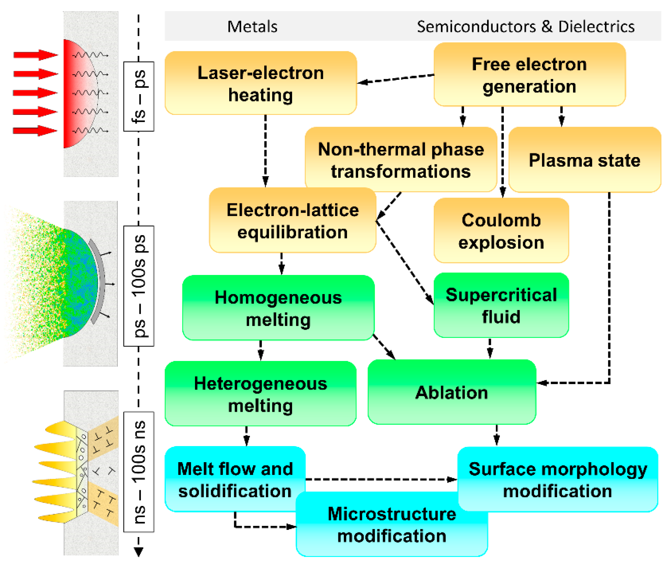
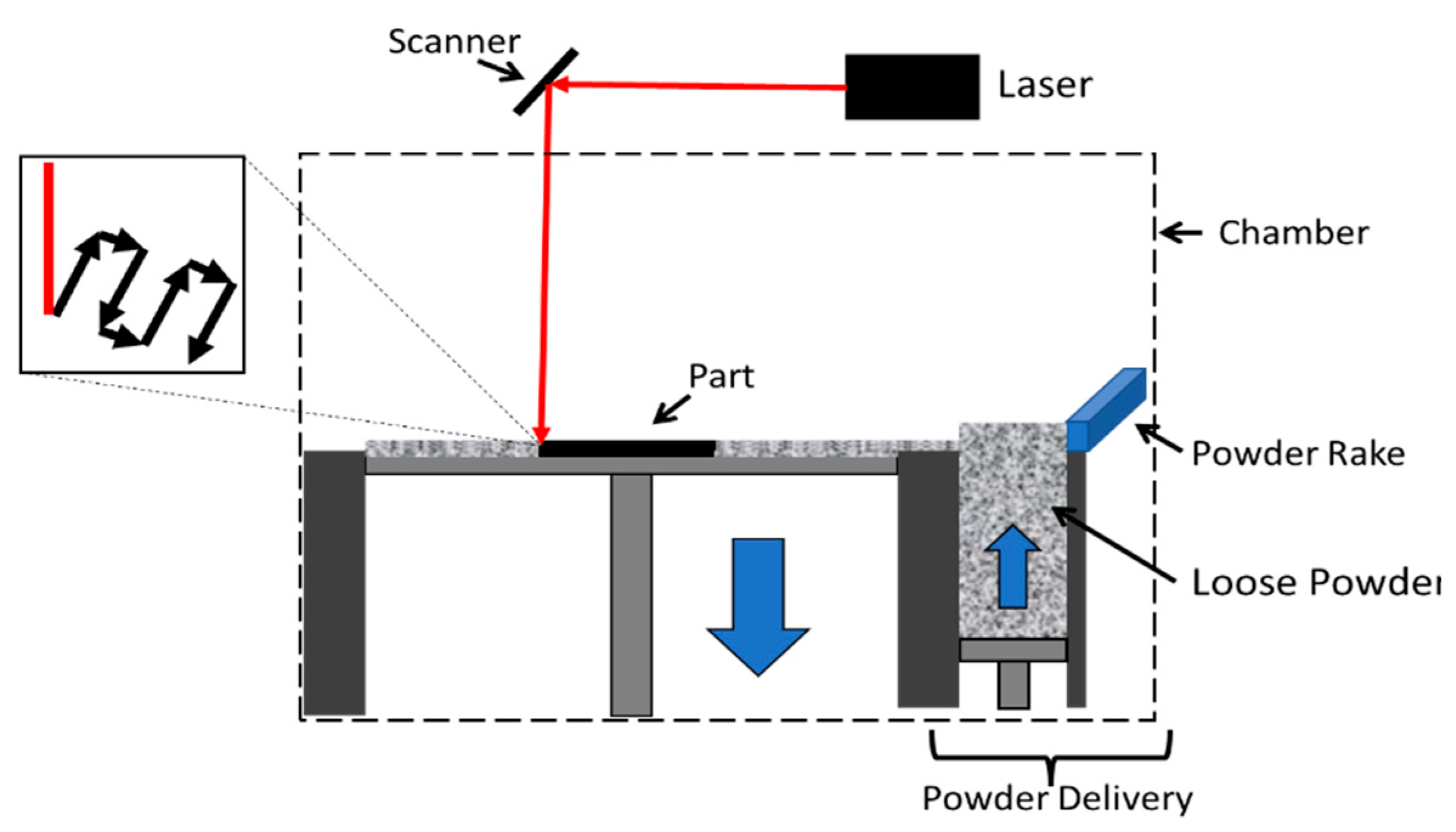
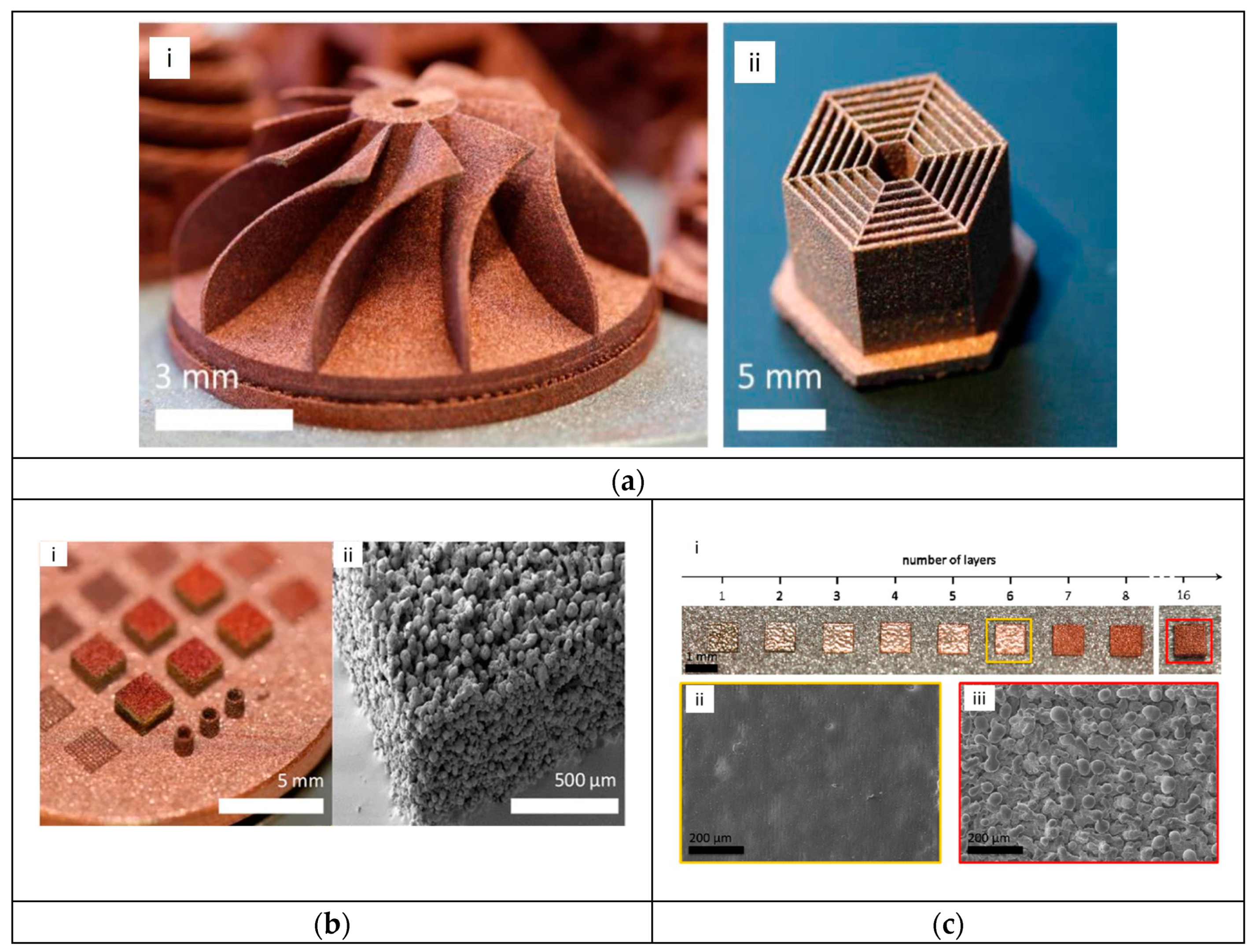
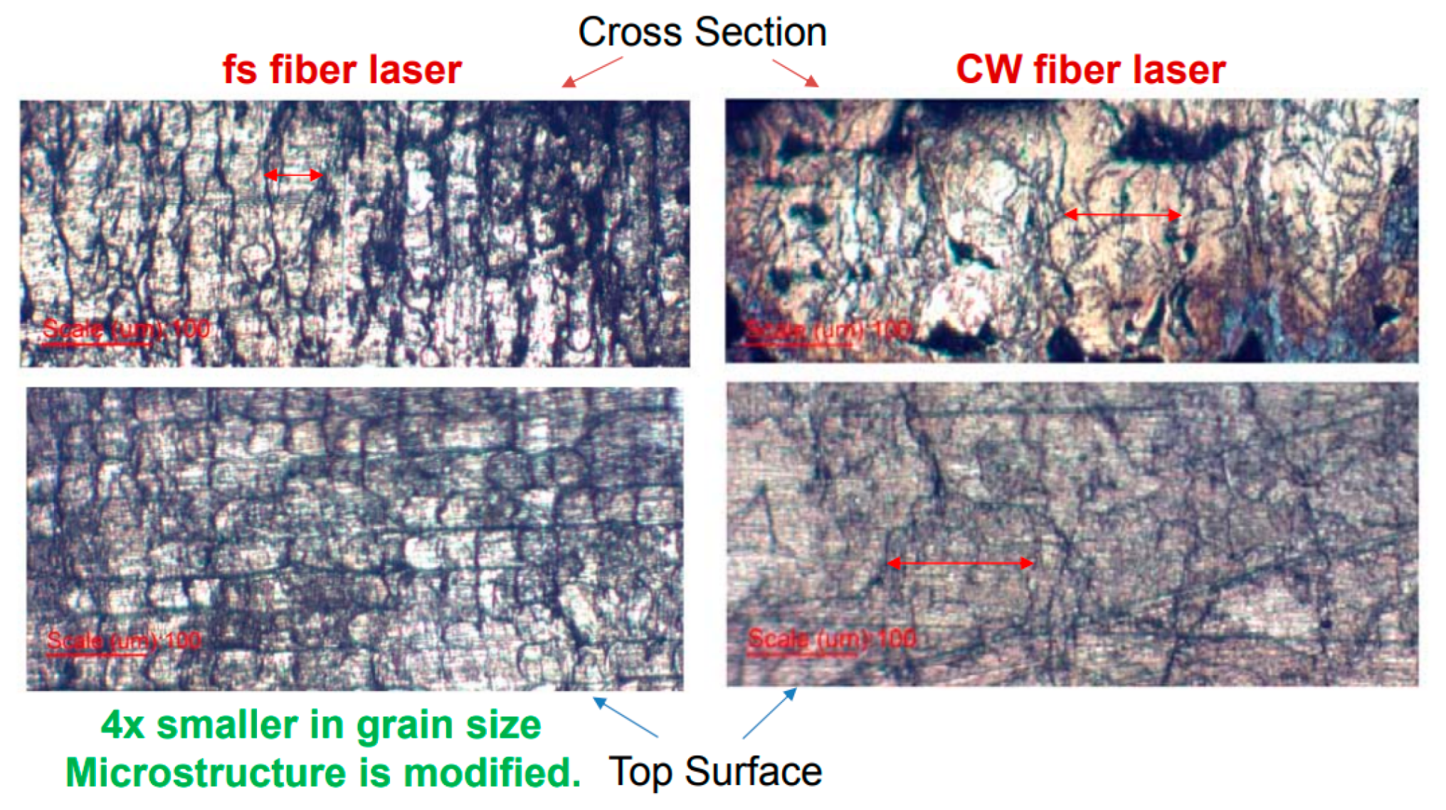
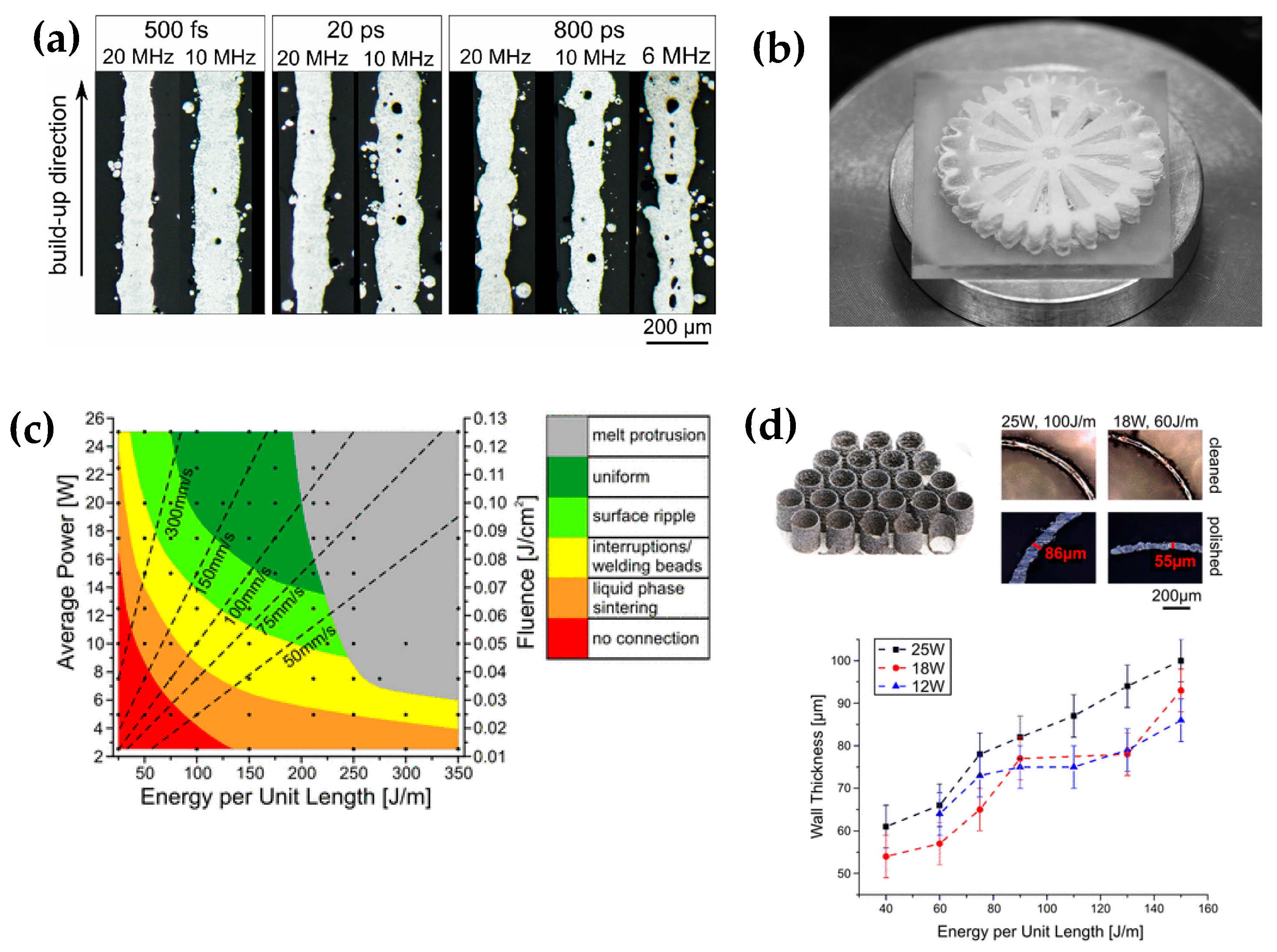
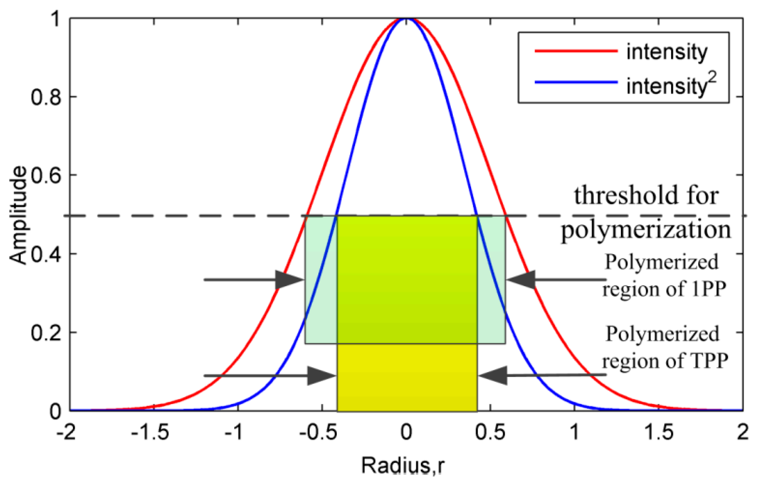
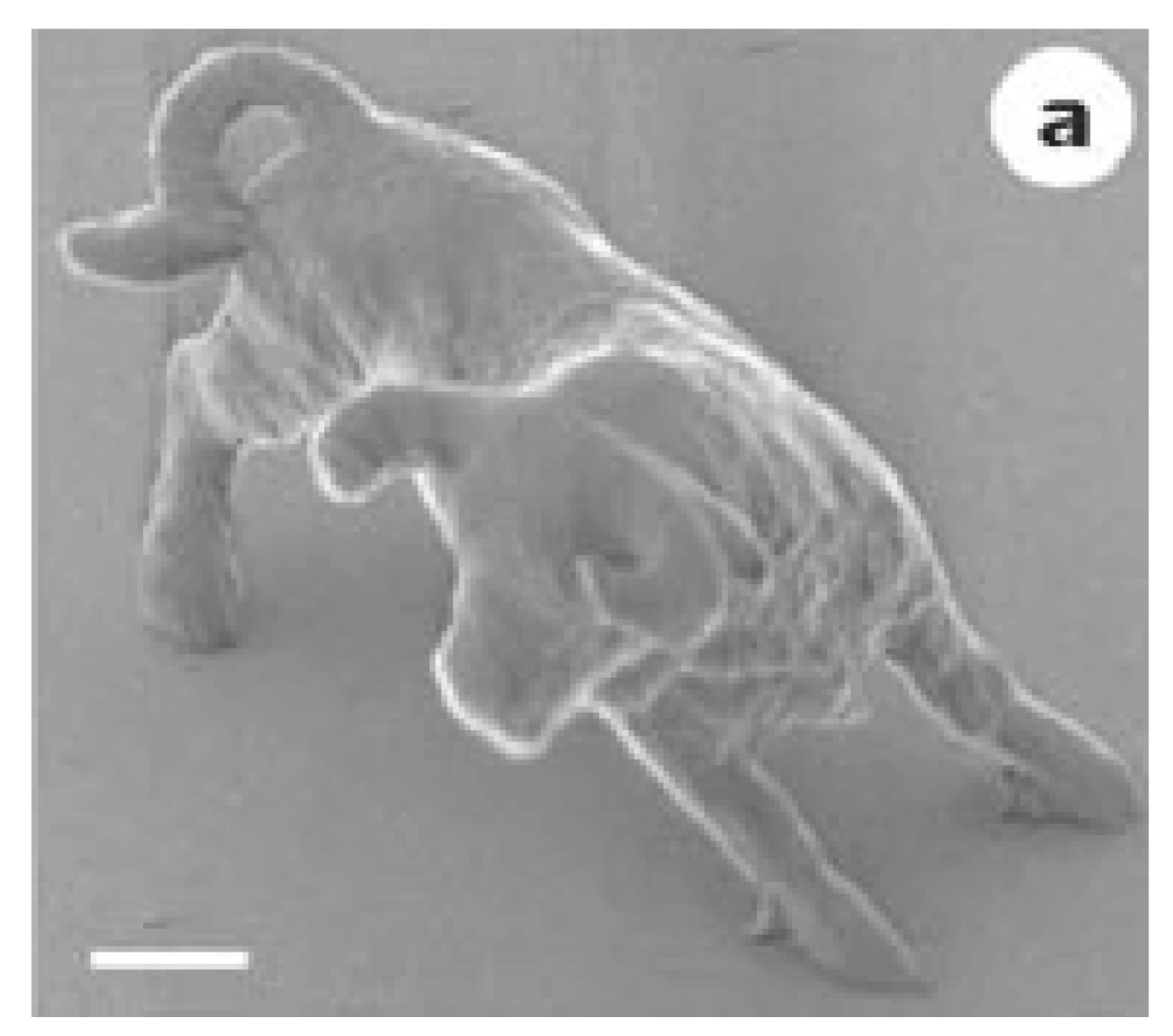
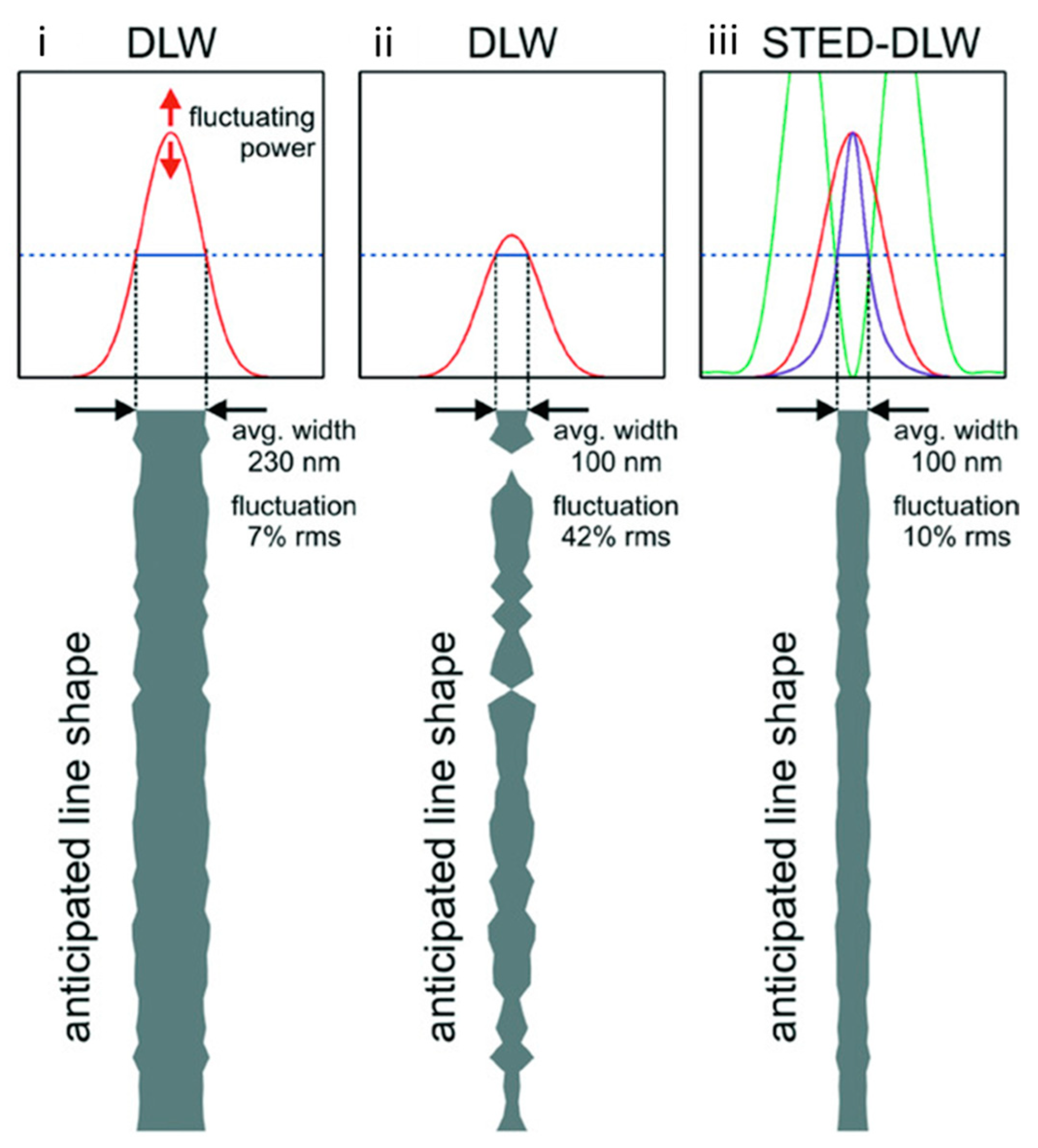
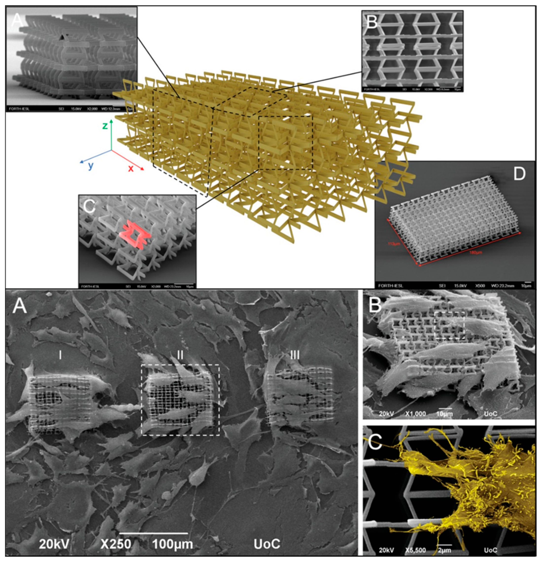
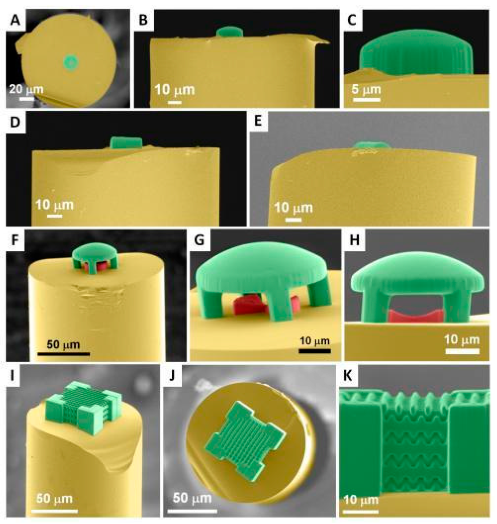
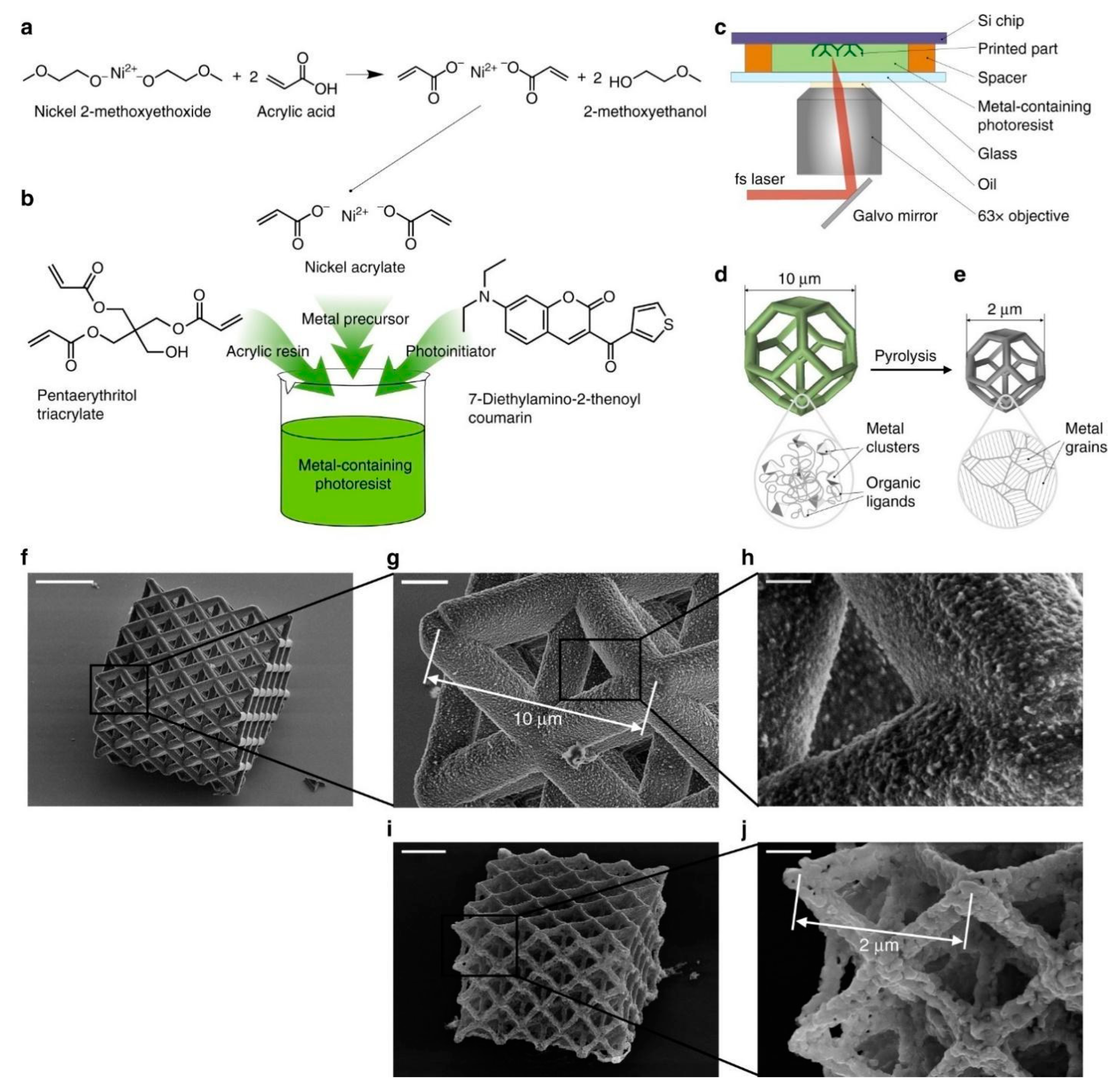
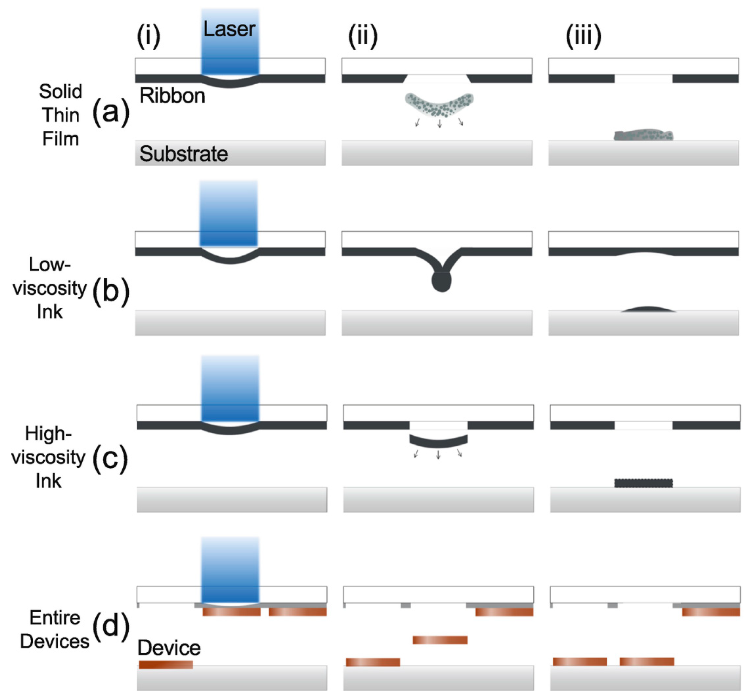
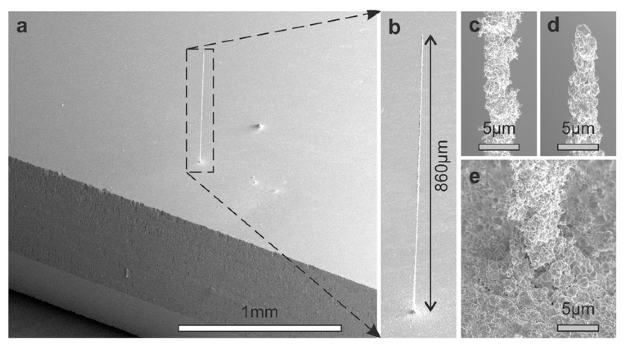
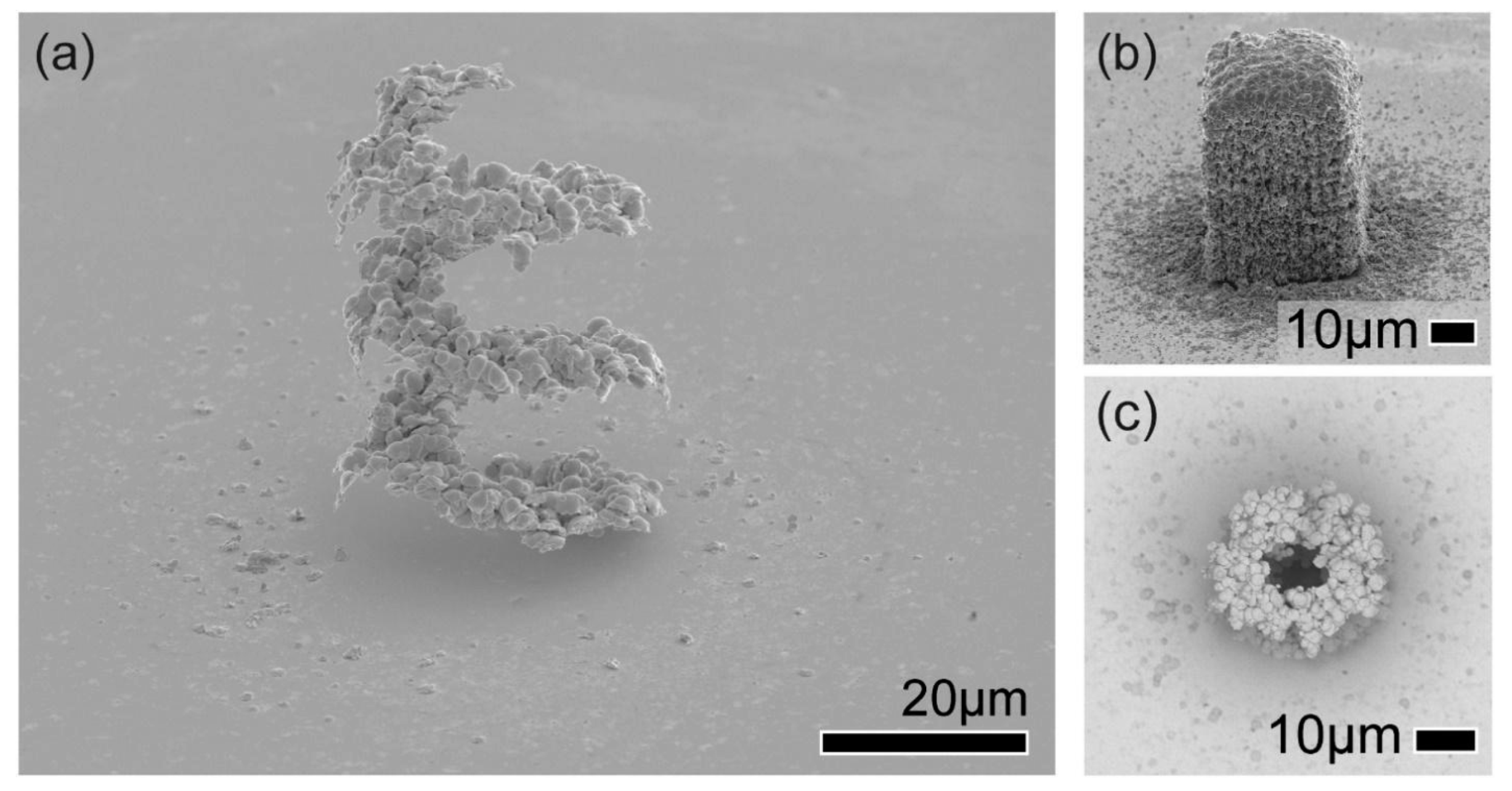
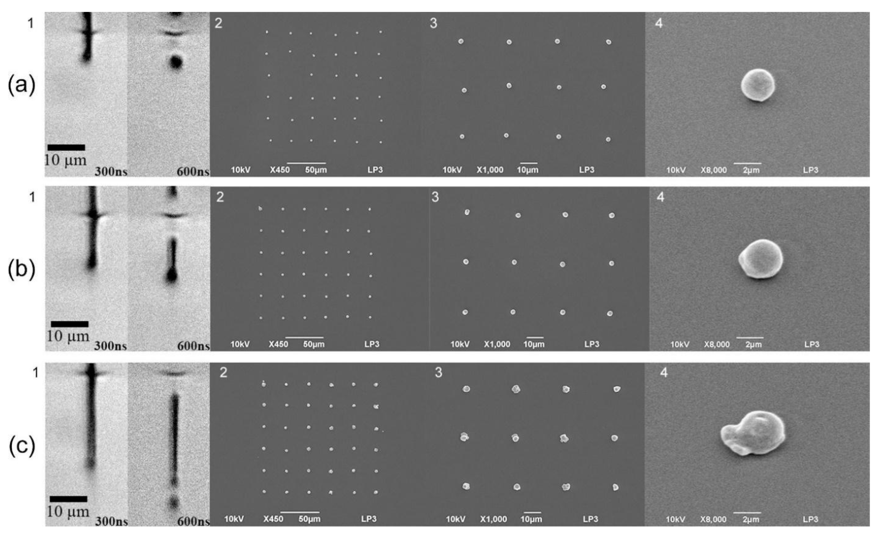
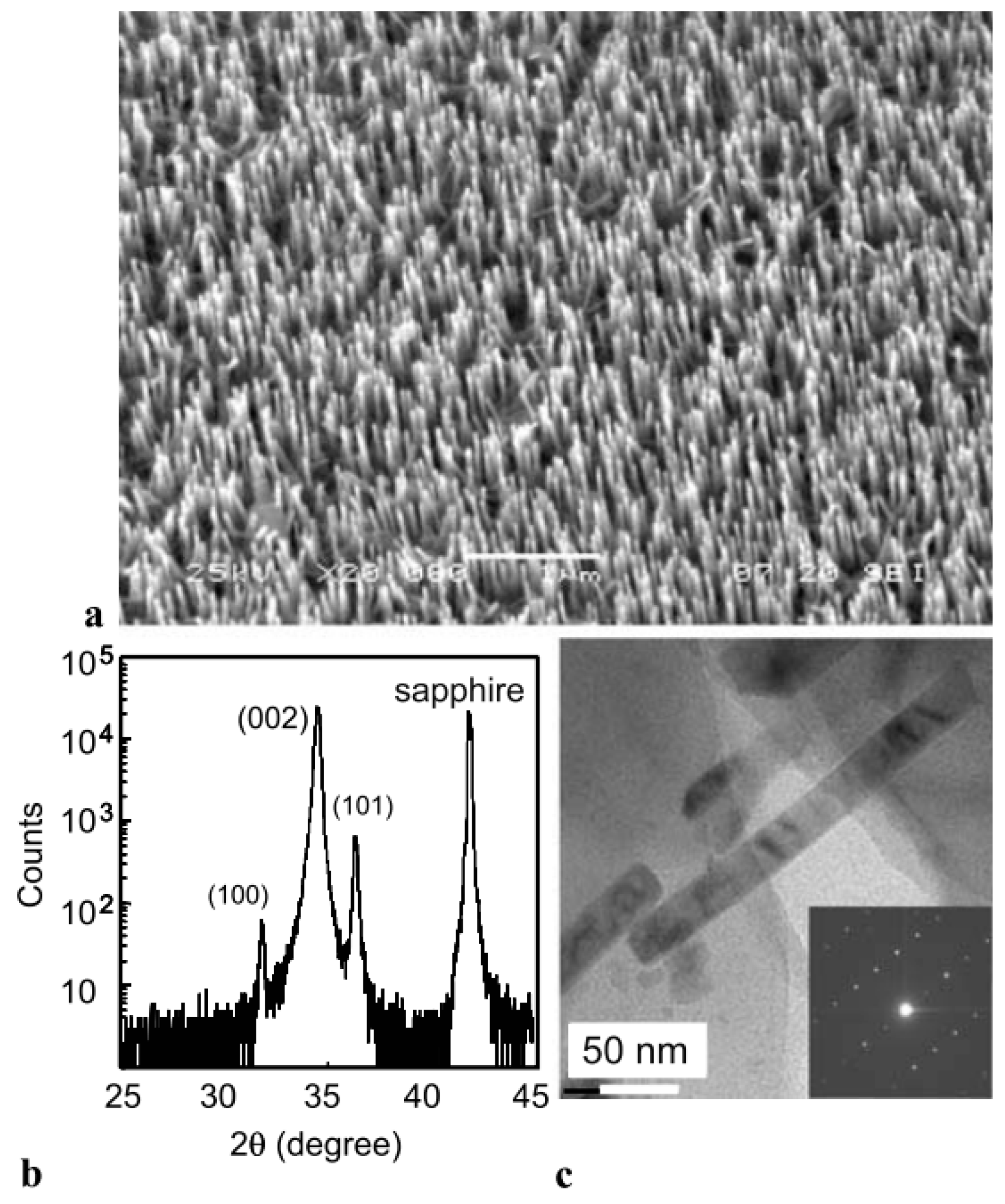
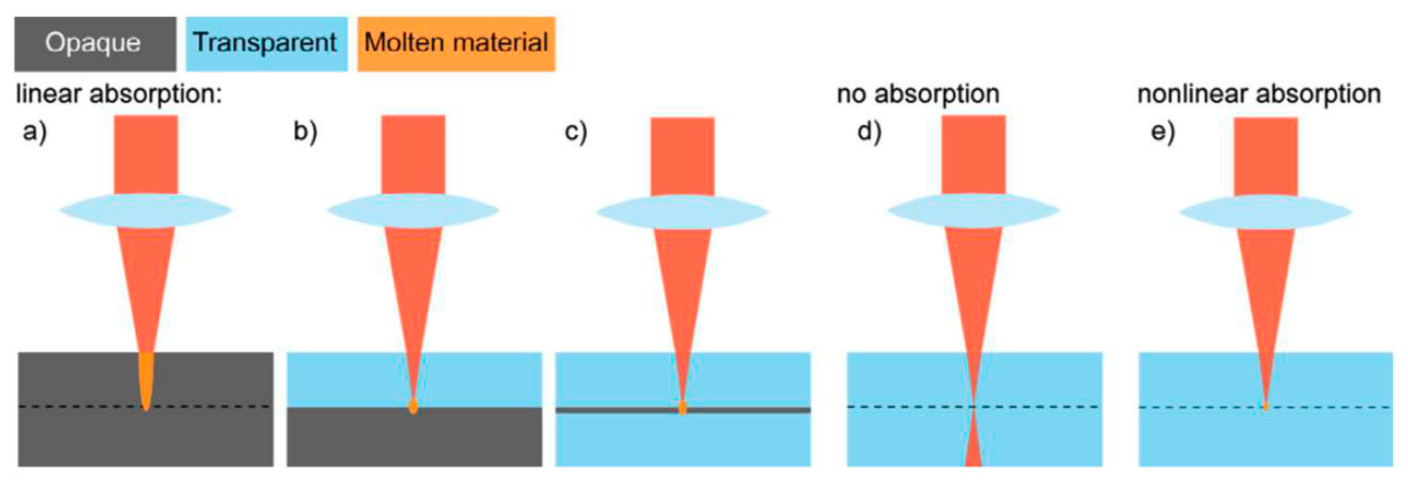
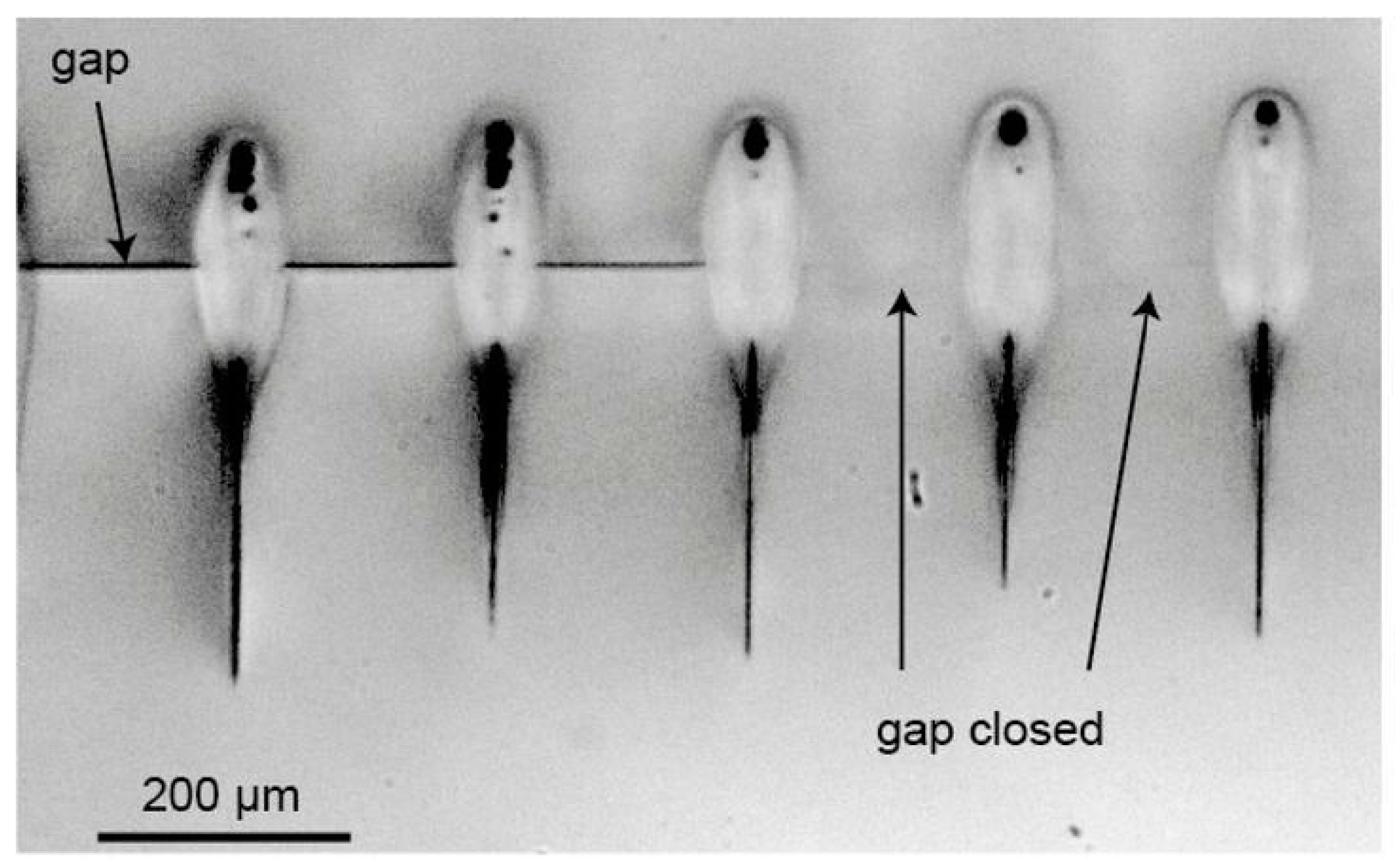
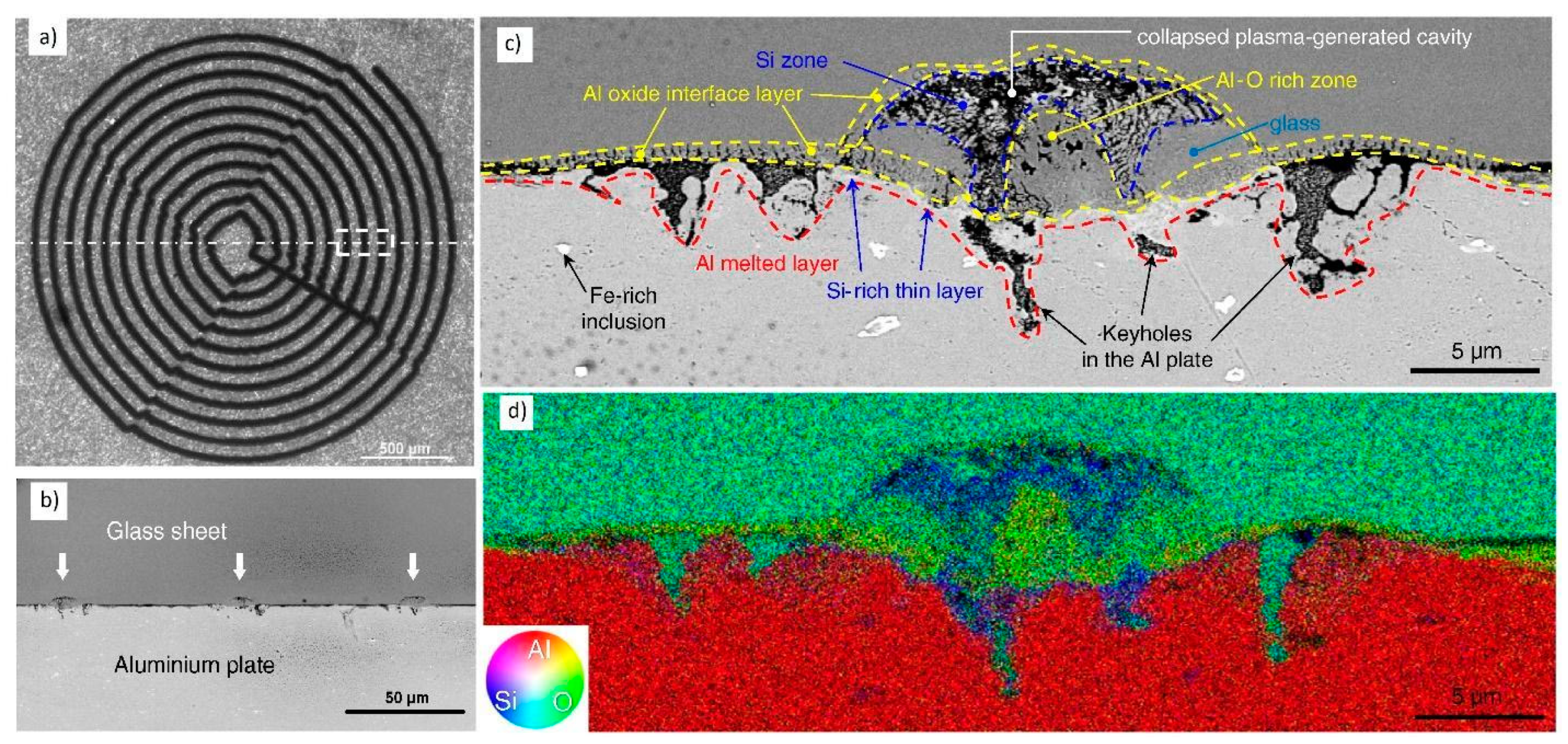
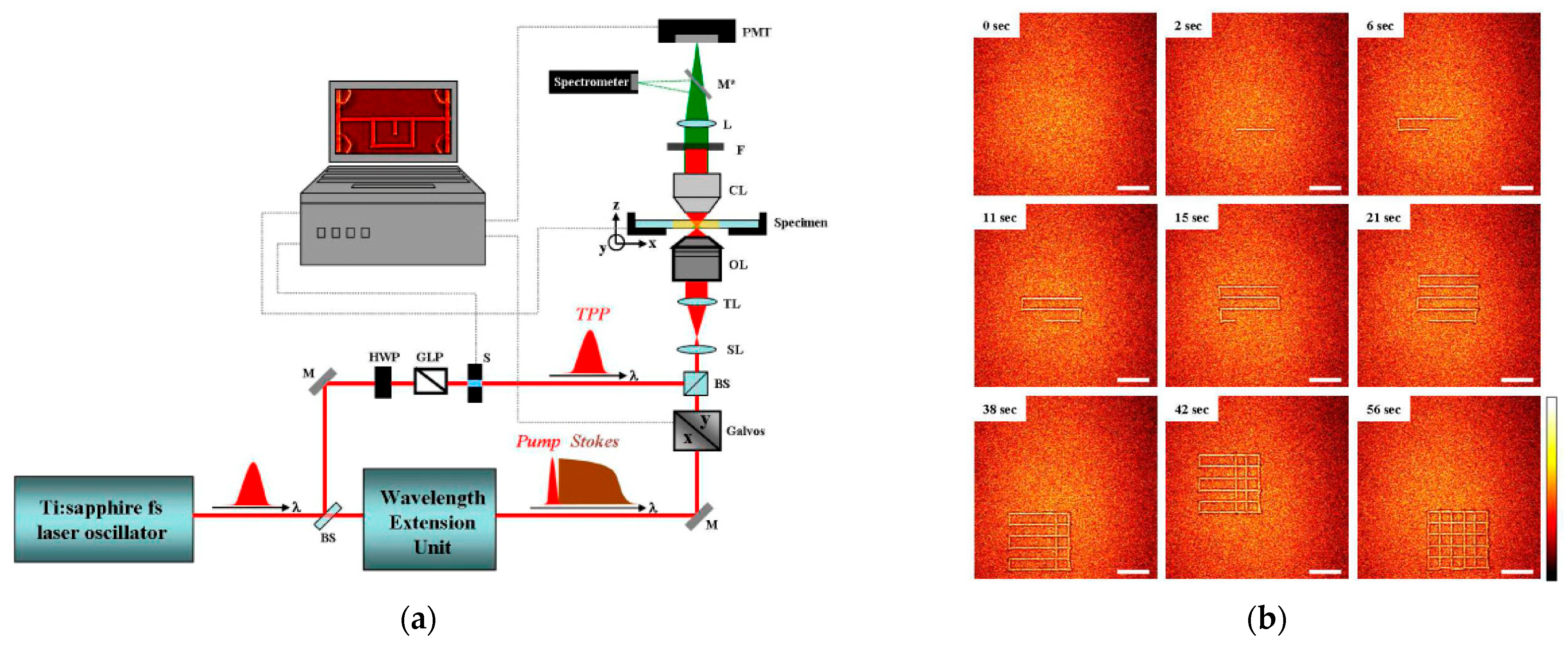
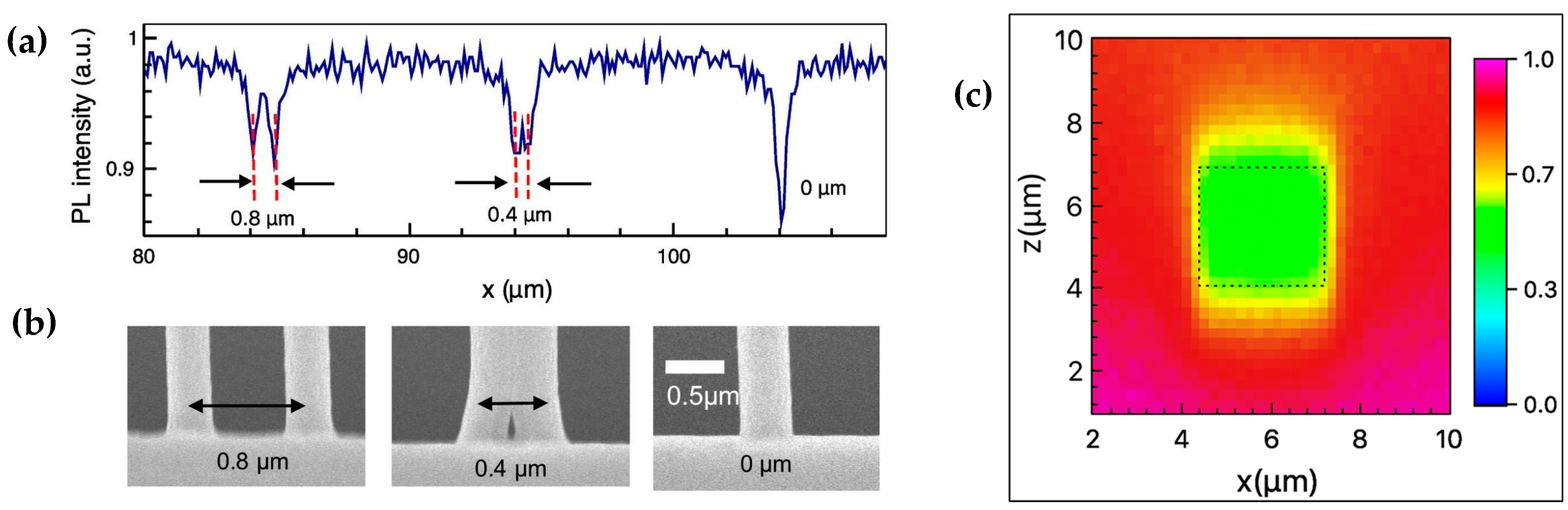
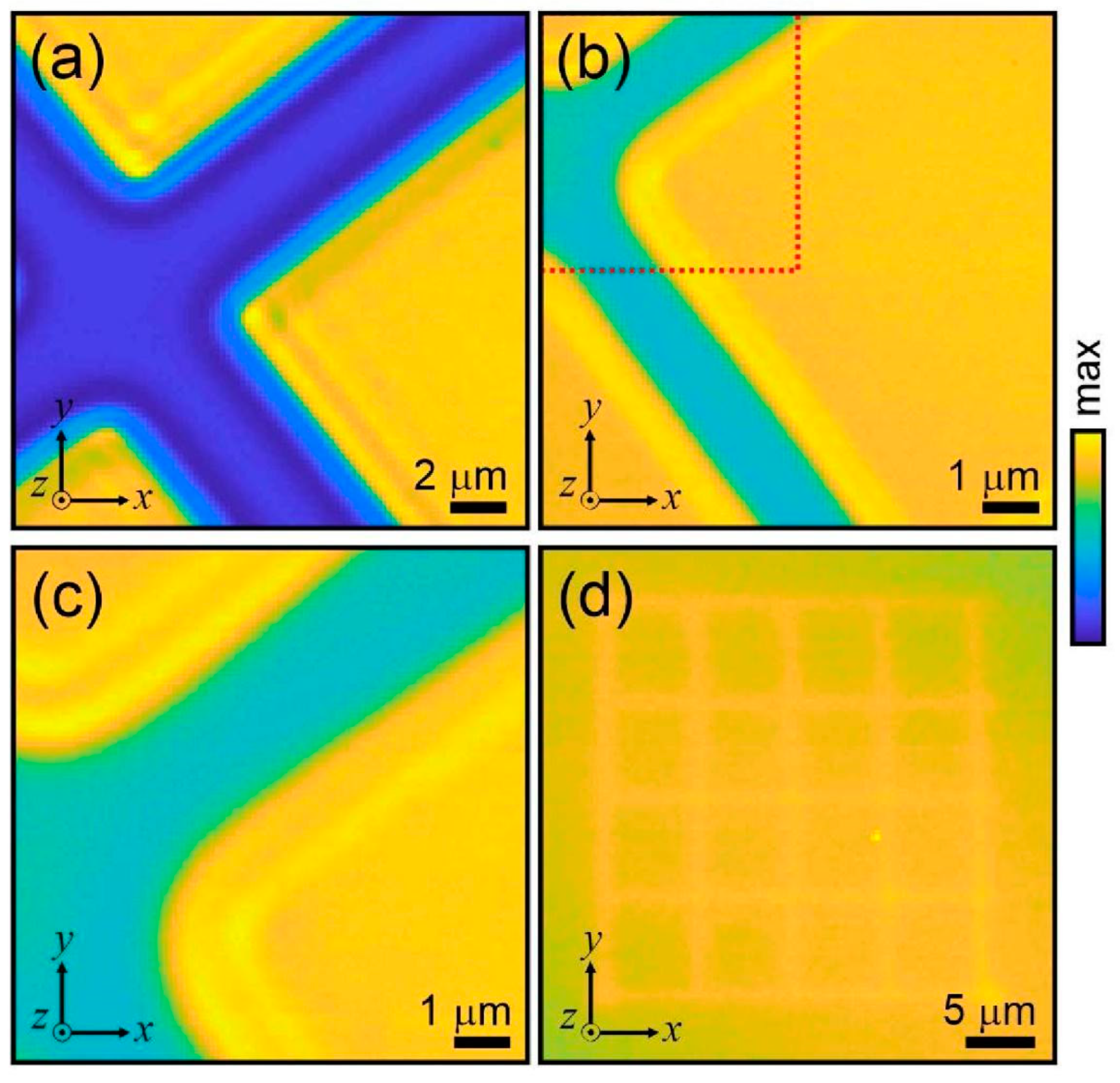
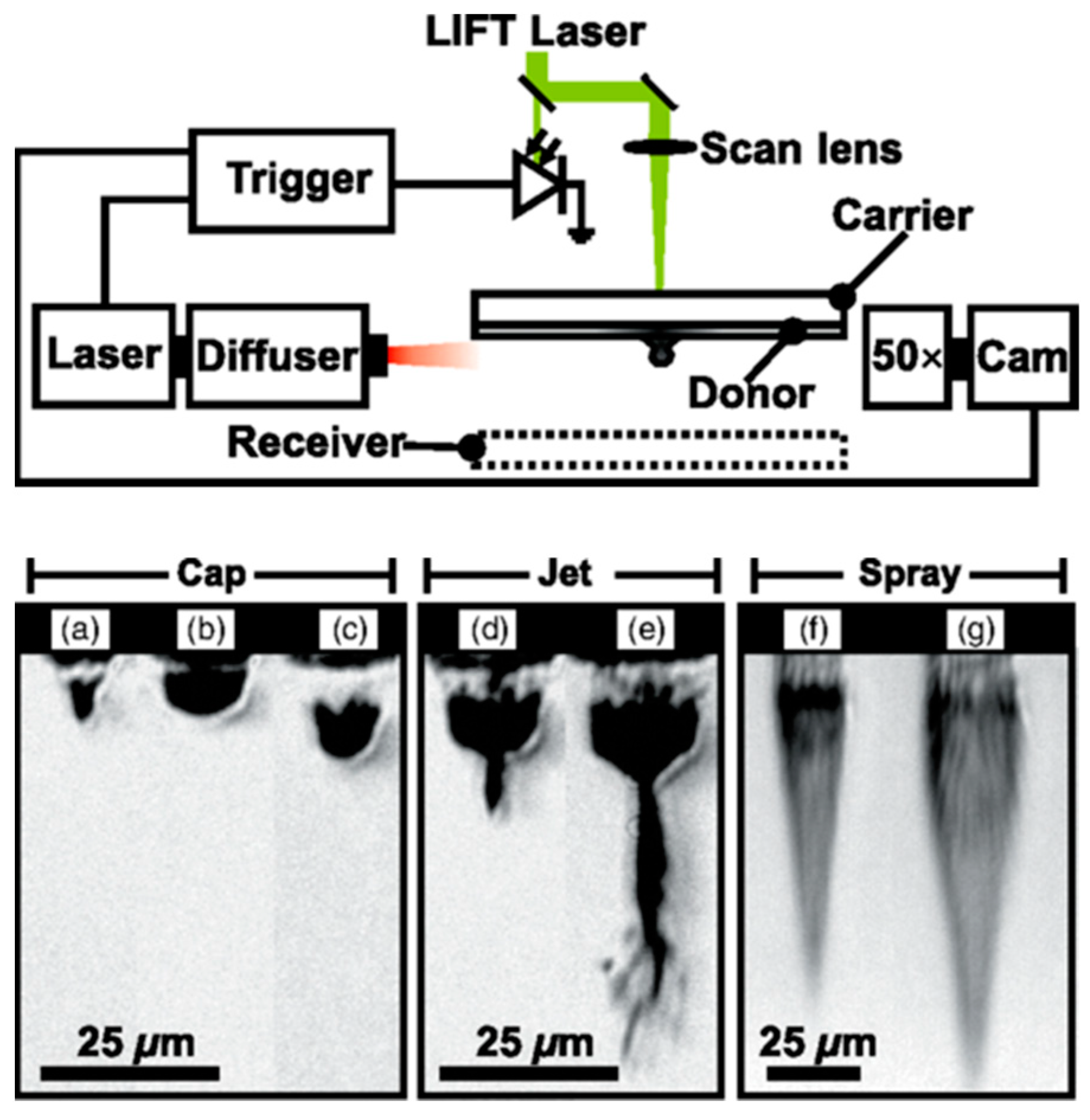
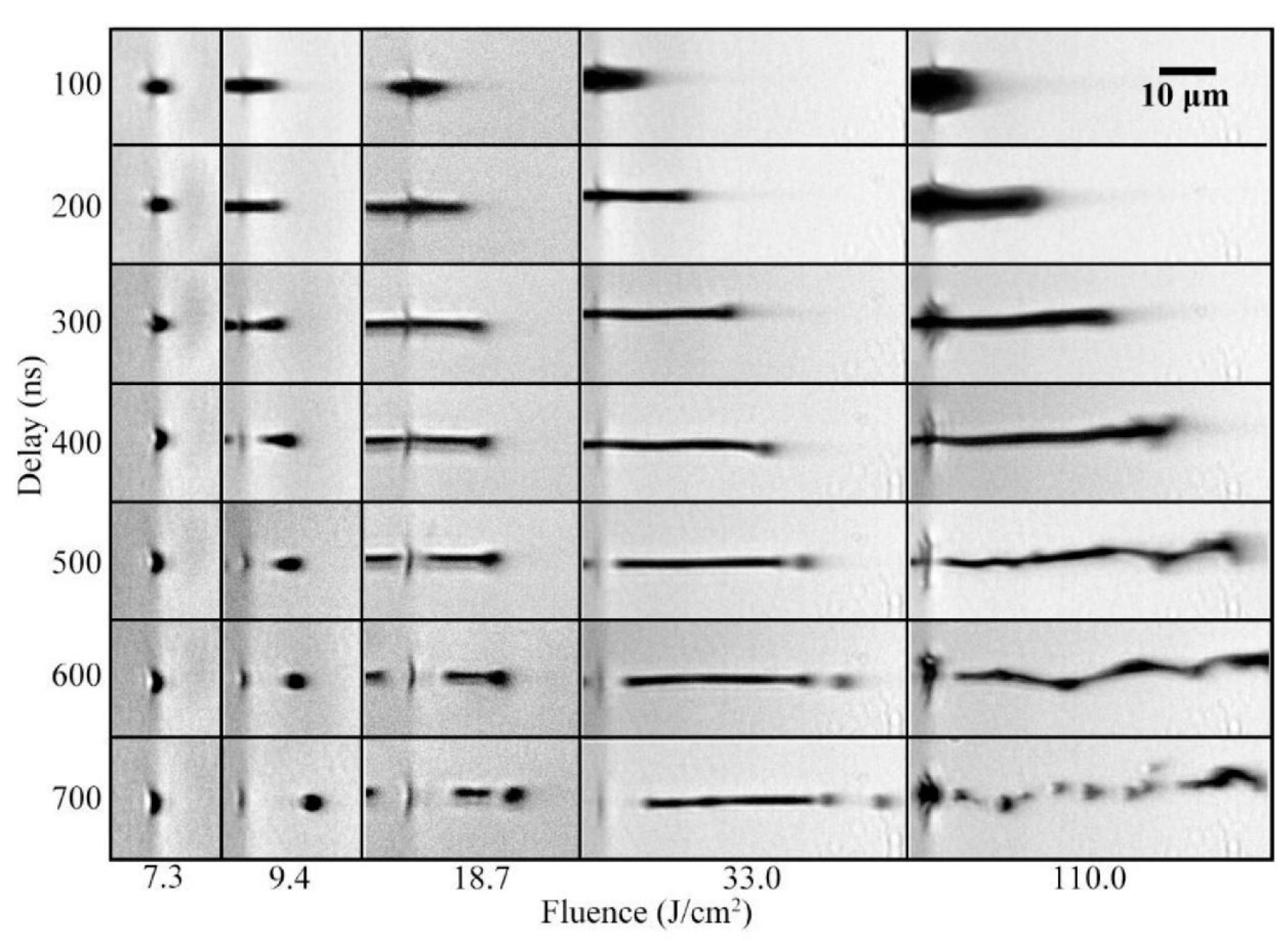
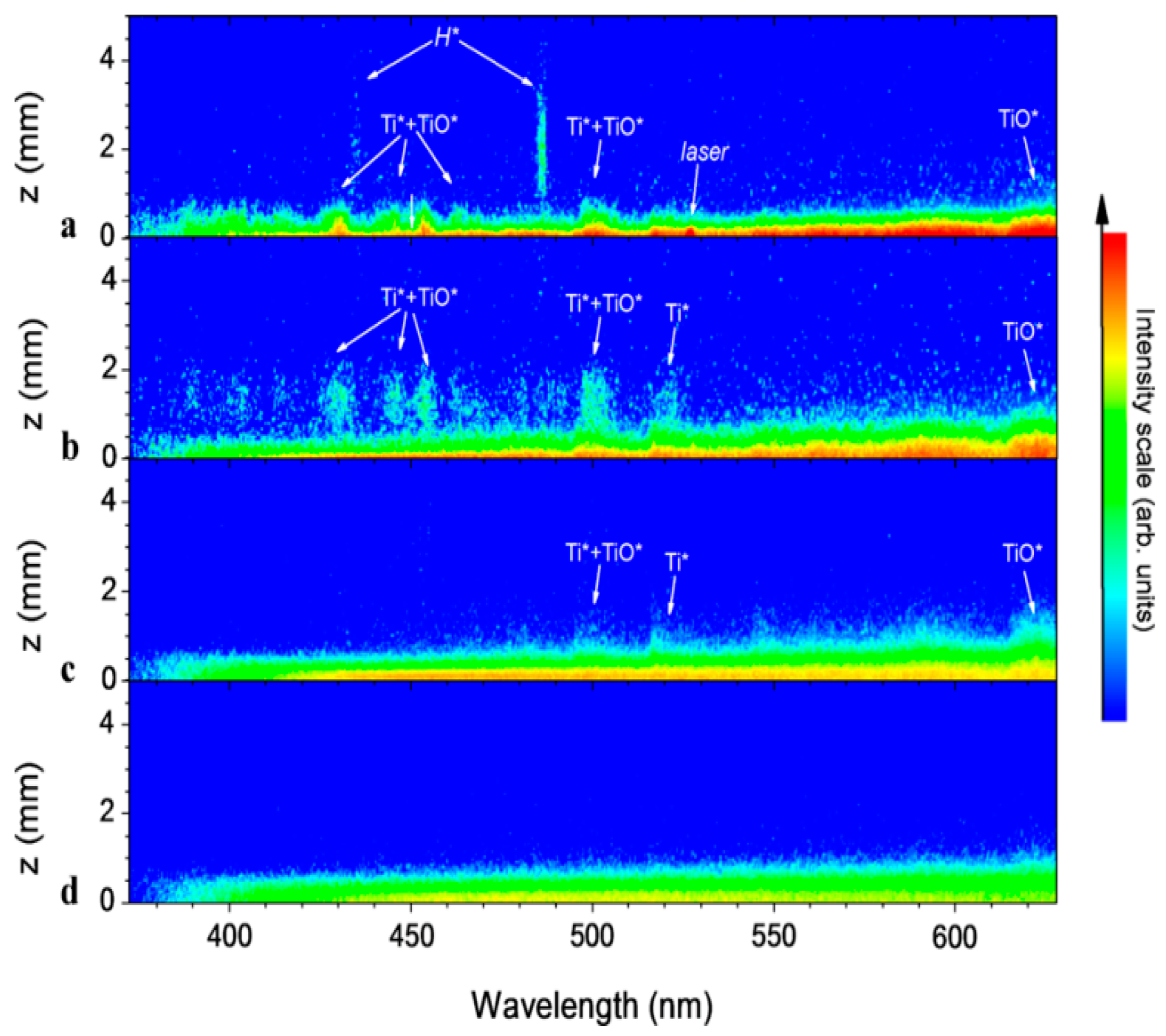
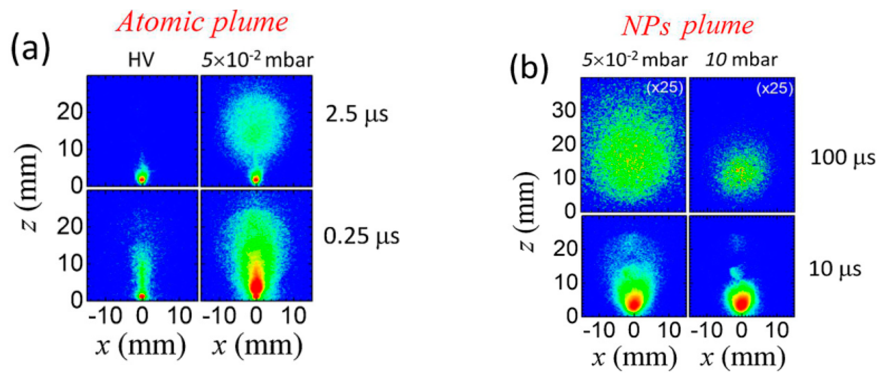
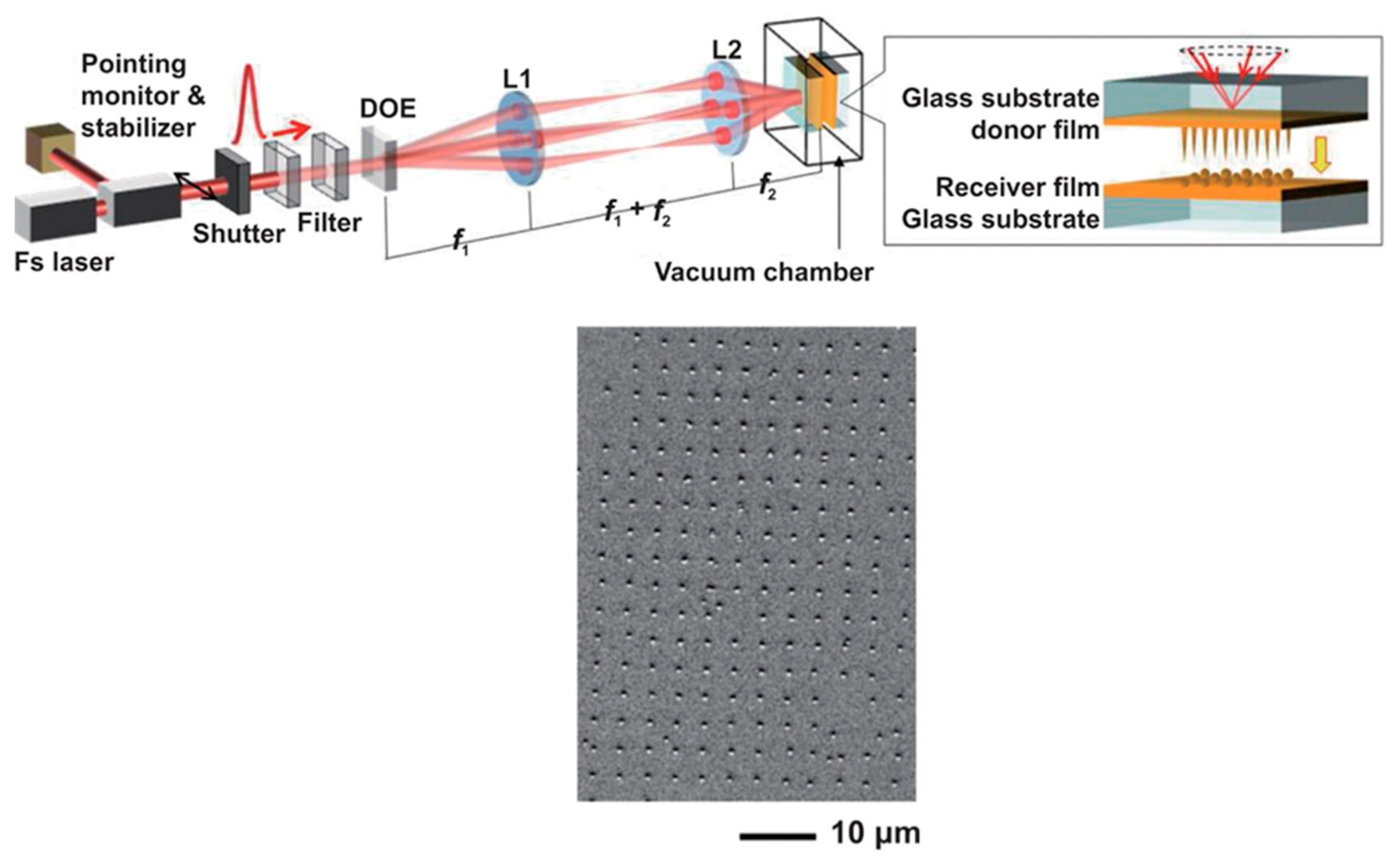
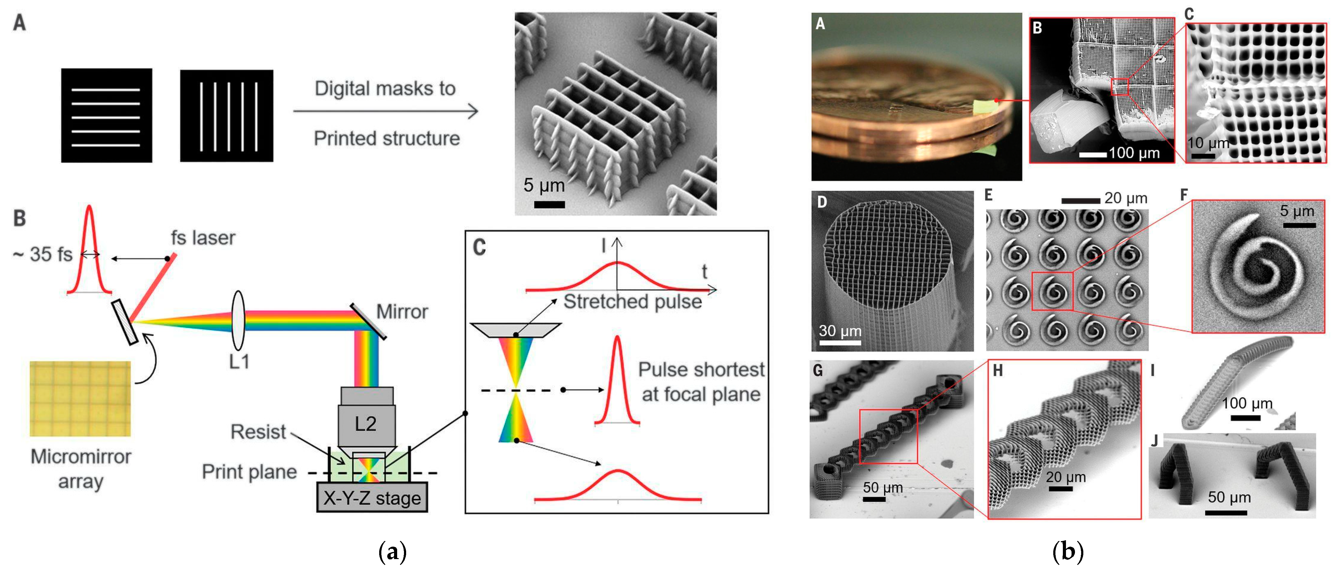
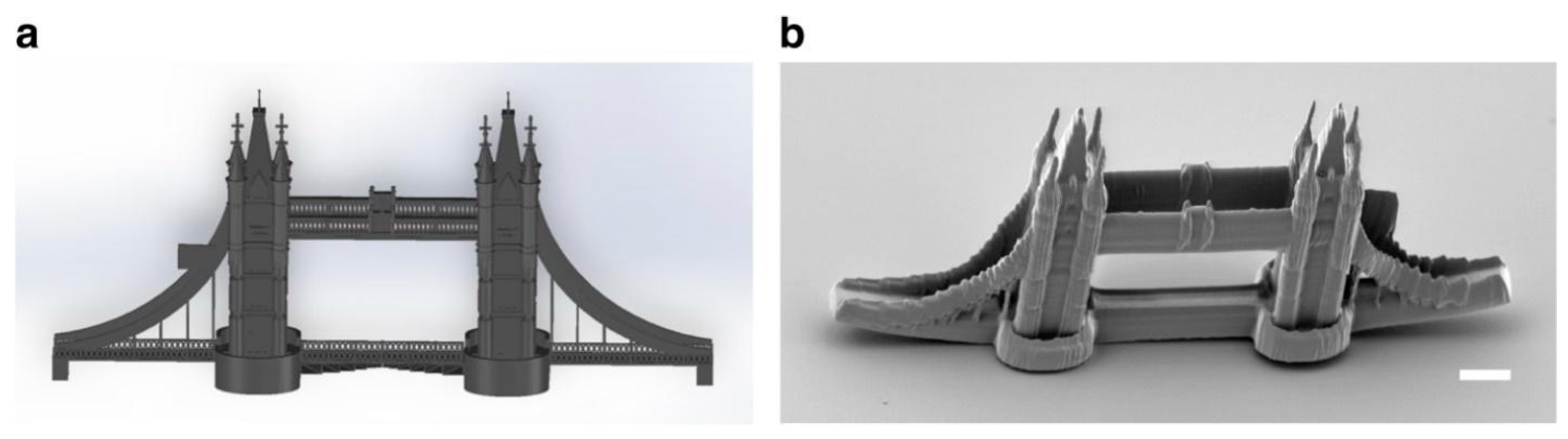
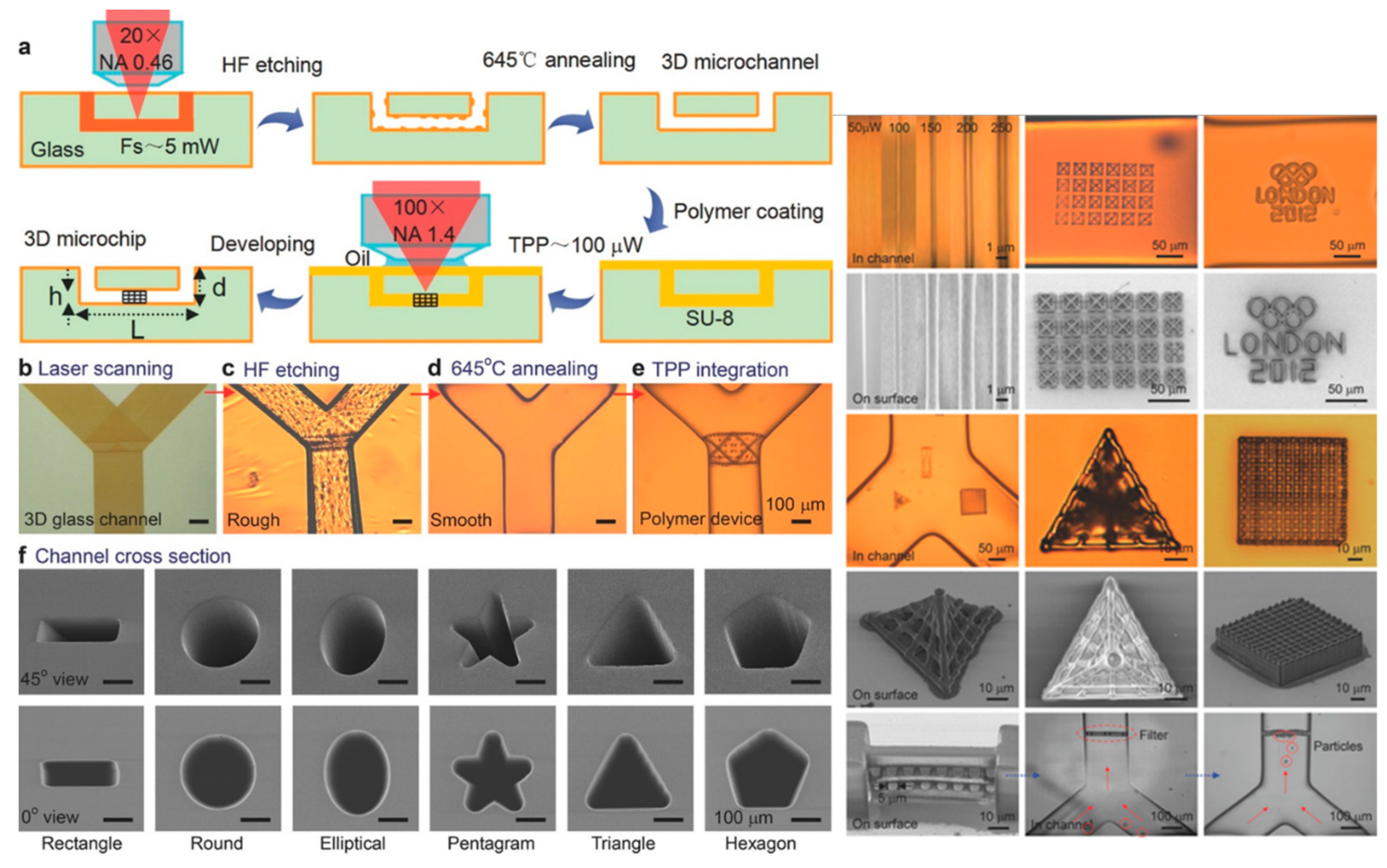
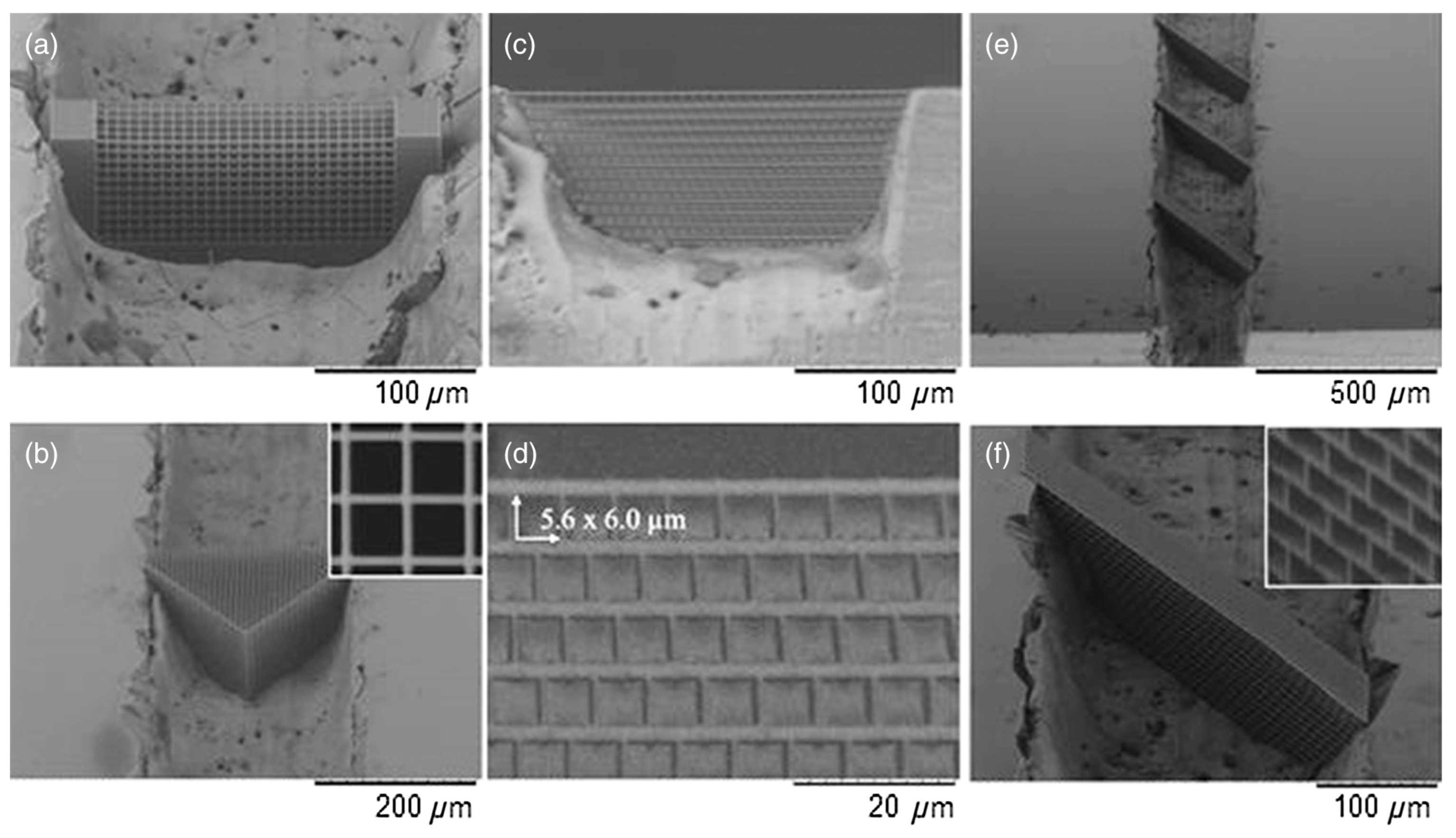
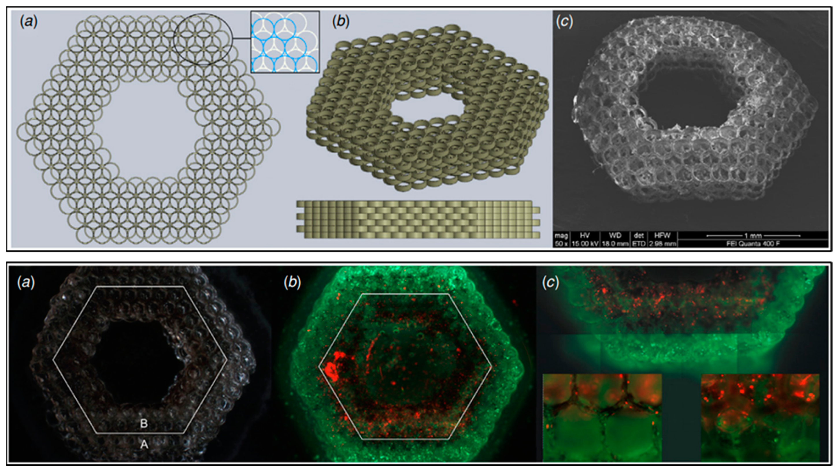
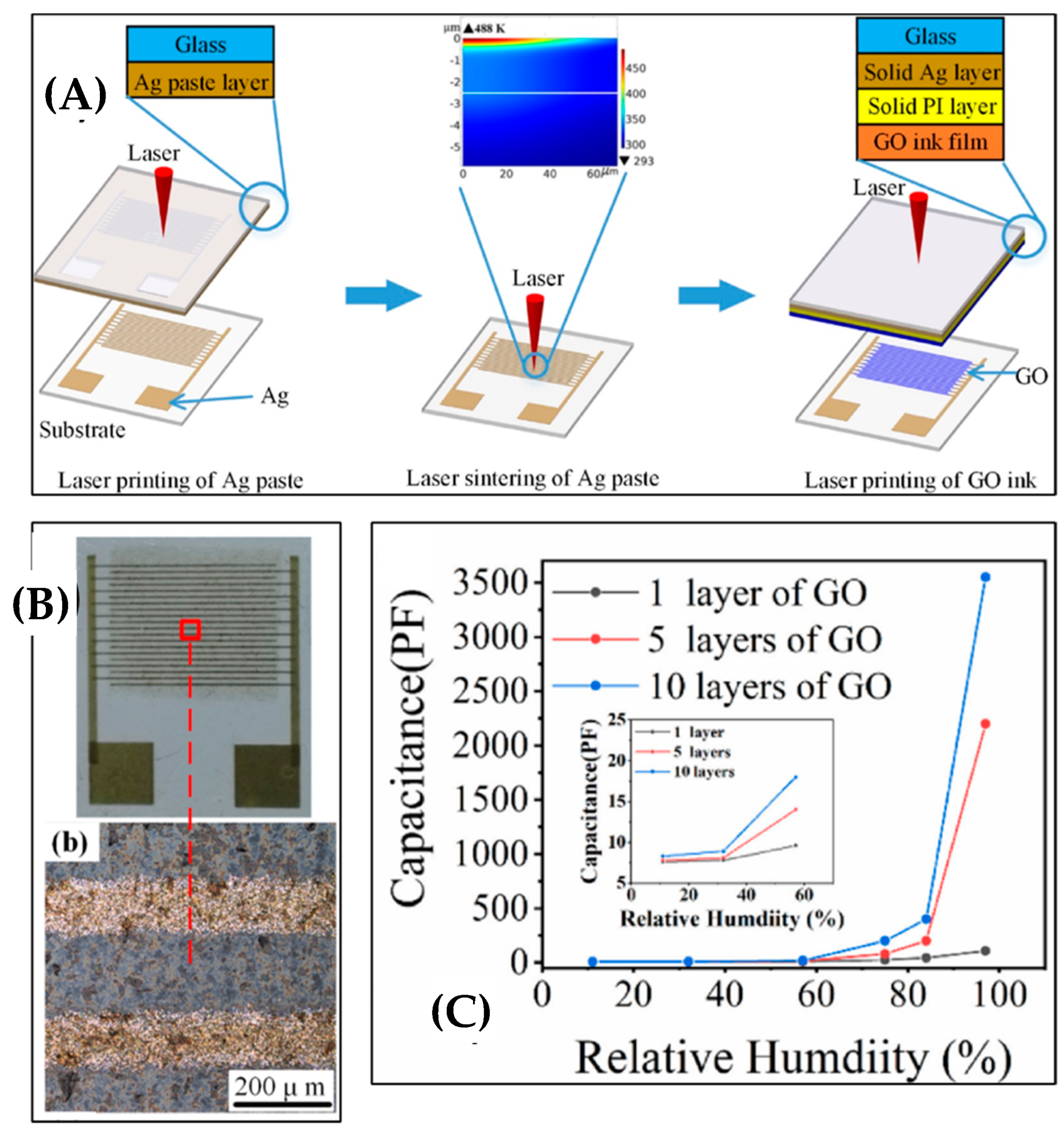
Table 1.
Summary of recent work in laser melting of powder by ultrafast laser.
| Material | Justification for Ultrashort Pulse | Wavelength | Average Power | Pulse Duration | Repetition Rate | Pulse Energy | Scanning Velocity |
|---|---|---|---|---|---|---|---|
| Borosilicate glass [93] | Controlled thermal diffusion in bulk, shorter resolidification times | 1030 nm, frequency doubled to 515 nm | 11 W | Femtoseconds, unspecified | 20 MHz | 0.55 mJ | 20 mm/s |
| Al-Li, Al-Si [94,95,99] | Stronger refinement of microstructure, smaller melt pool and higher shape accuracy, reduced evaporation of Li in-process. | 1030 nm | 25–30 W | 500 fs–800 ps | 6–20 MHz | 1.5 µJ | 700 mm/s |
| UHMWPE [96] | Multi-photon absorption for more localized energy deposition, improved ultimate tensile strength. | 1030 nm | 30 W | 500 fs | 10 MHz | 3 µJ | 100 to 500 mm/s |
| Bimetallic (12Cr2Si/9Cr1Mo, SS316L/SA508) [97] | Conventional L-PBF is challenged by dissimilar materials. | unspecified | 200 W | Femtosecond, unspecified | unspecified | unspecified | unspecified |
| Rhenium, Hafnium diboride, Zirconium diboride [98] | High melting temperatures (5596 C, 3250 C, 3246 C, respectively). | 1030 nm | Up to 35 W | 400 fs | 1 MHz | Up to 35 µJ | mm/s |
Table 2.
Summary and comparison of ultrafast laser additive manufacturing techniques.
| Technique | Materials | Dimensional Scales | Applications | Main Challenges |
|---|---|---|---|---|
| Selective Laser Melting |
| 100 m to cm |
|
|
| Multiphoton Lithography |
| nm to mm |
|
|
| Laser-Induced Forward Transfer |
| Single-digit um depositions, stackable to mm |
|
|
| Pulsed Laser Deposition |
| nm thick films, atomically smooth films |
|
|
| Welding/Joining |
| 10 s of um to cm |
|
|
Disclaimer/Publisher’s Note: The statements, opinions and data contained in all publications are solely those of the individual author(s) and contributor(s) and not of MDPI and/or the editor(s). MDPI and/or the editor(s) disclaim responsibility for any injury to people or property resulting from any ideas, methods, instructions or products referred to in the content. |
© 2023 by the authors. Licensee MDPI, Basel, Switzerland. This article is an open access article distributed under the terms and conditions of the Creative Commons Attribution (CC BY) license (https://creativecommons.org/licenses/by/4.0/).
Share and Cite
MDPI and ACS Style
Saunders, J.; Elbestawi, M.; Fang, Q. Ultrafast Laser Additive Manufacturing: A Review. J. Manuf. Mater. Process. 2023, 7, 89. https://doi.org/10.3390/jmmp7030089
AMA Style
Saunders J, Elbestawi M, Fang Q. Ultrafast Laser Additive Manufacturing: A Review. Journal of Manufacturing and Materials Processing. 2023; 7(3):89. https://doi.org/10.3390/jmmp7030089
Chicago/Turabian StyleSaunders, Jacob, Mohammad Elbestawi, and Qiyin Fang. 2023. "Ultrafast Laser Additive Manufacturing: A Review" Journal of Manufacturing and Materials Processing 7, no. 3: 89. https://doi.org/10.3390/jmmp7030089