Article

Effect of the ZnSnO/AZO Interface on the Charge Extraction in Cd-Free Kesterite Solar Cells

1
Department of Materials Science and Solar Energy Research Center (MIB-SOLAR), University of Milano-Bicocca, Via Cozzi 55, 20125 Milano, Italy
2
ENEA (Agenzia Nazionale per le Nuove Tecnologie, l’Energia e lo Sviluppo Economico Sostenibile) C.R. CASACCIA, Via Anguillarese 301, 00123 Roma, Italy
3
Dipartimento di Ingegneria Elettrica e delle Tecnologie dell’Informazione, Università degli Studi di Napoli Federico II, Corso Umberto I 40, 80138 Napoli, Italy
*
Author to whom correspondence should be addressed.
Energies 2023, 16(10), 4137; https://doi.org/10.3390/en16104137
Submission received: 31 March 2023 / Revised: 5 May 2023 / Accepted: 15 May 2023 / Published: 17 May 2023
(This article belongs to the Collection Feature Papers in Advanced Energy Materials)

Abstract

:
Cu2ZnSnS4 (CZTS) is a promising absorber material to produce thin film solar cells thanks to its high absorption coefficient, low cost and low toxicity. CdS is commonly used as a buffer layer for CZTS solar cells but, beyond its toxicity, it has a nonoptimal band alignment with CZTS. ZnxSn1−xO (ZTO), based on earth-abundant and nontoxic elements and with a large and tunable band gap, is a suitable alternative buffer layer. In this paper, the atomic layer deposition (ALD) of ZTO was employed by testing different compositions and thicknesses. ALD not only leads to very compact and homogenous ZTO layers (enabling tuning the stoichiometry of the ZTO so prepared) but also makes the i-ZnO layer (usually sandwiched between the buffer layer and the transparent contact) redundant and detrimental. Through SCAPS simulation and impedance measurements, the ZnSnO/AZO interface impact on the Cd-free kesterite solar cells’ performances has been investigated, highlighting its leading role in achieving an effective charge extraction and the detrimental effect of the i-ZnO layer. With this approach, a solar cell based on an architecture simpler and more eco-friendly than the conventional one has been produced with comparable efficiencies.

1. Introduction

Kesterite absorber materials such as Cu2ZnSnS4 (CZTS), Cu2ZnSn(S,Se)4 (CZTSSe) and Cu2ZnSnSe4 (CZTSe) are particularly promising for the development and large-scale production of thin-film solar cells, mainly due to their similarity to the already commercially available copper indium gallium diselenide CuInGaSe2 (CIGS) solar cell technologies, while consisting of earth-abundant, low-cost and low-toxicity elements [1]. Kesterite attracted the attention of photovoltaic (PV) research as a p-type semiconductor thanks to its high absorption coefficient (over 104 cm−1) and its tunable bandgap energy between 1.0 and 1.6 eV, depending on the [S]/([S] + [Se]) composition and the cation disordering level [2,3]. These optoelectronic properties make kesterite a good candidate for tandem device structures and high-efficiency solar cells [4]. The current record efficiency for the low bandgap (1.1 eV) selenized kesterite (CZTSSe) is at 13.6%, while the highest efficiency for the pure sulfide kesterite (CZTS), with wide bandgap (1.5 eV), is at 11% [5]. Several ongoing studies reported in the literature aim to increase the record efficiency of kesterite-based solar cells, which is required for industrial implementation. Among these, many studies are directed toward the design of a buffer layer that can improve charge extraction and, thus, all PV parameters [6]. To date, CdS is commonly used as a buffer layer for kesterite thin film solar cells. In addition to being toxic, hazardous and not ideal for environment-friendly processing, CdS introduces unwanted light absorption and has a nonoptimal band alignment with CZTS, which results in an open circuit voltage (Voc) deficit [7,8,9,10,11,12]. To reduce charge carrier recombination and to increase the current density (Jsc) and the Voc, the optimal n-type partner for kesterite should have a wider band gap compared to CdS [7]. The use of an alternative material to CdS, such as ZnSnO (ZTO) [13], Zn(O,S) [14] and TiO2 [15], would, therefore, improve charge transport and make the devices cadmium-free [2]. Especially ZnxSn1−xO (ZTO) is an interesting alternative: it is appealing for scale production as it contains only earth-abundant and nontoxic constituents, [16] and it has a large and tunable band gap, controllable by varying the Zn to Sn ratio [17]. Already in 2012, several research groups successfully used ZTO as a buffer layer for CIGS-based solar cells, matching and exceeding the performance achieved with CdS [18,19]. Since 2016, experimental results comparable to CdS have been obtained by depositing ZTO on CZTS with different thicknesses and compositions [20,21,22]. Sputter deposition and atomic layer deposition (ALD) have already been successfully employed in the ZTO synthesis [20,21,23,24,25,26]. ALD is a deposition technique compatible with the requirements of the kesterite solar cells production and, compared to sputtering, allows for very compact and homogenous ZTO layers with precise control of stoichiometry [20]. Li et al. first reported the use of ZTO as a buffer layer in a CZTSSe solar cell, achieving maximum efficiency of 8.60%, with Sn/(Sn + Zn) = 0.167 and with a thickness of ~50 nm [21]. However, since selenium-based kesterite yields better device performance, less research has been focused on the effect of the ZTO layer in pure sulfide (CZTS) devices. Cui et al. obtained an efficiency of 9.3% using a 10 nm Zn0.77Sn0.23O buffer layer but with an expensive ITO top contact and with 110 nm of MgF2 as antireflection coating [20]. The highest efficiency of 10.2% has been obtained for pure-phase CZTS devices with ALD-ZTO buffer layers. However, these results were reached by using a complex and expensive device structure (Mo/CZTS/Al2O3/ZnSnO/i-ZnO/ITO/MgF2) with an Al2O3 passivation layer, which reduces interface recombination when sandwiched by CZTS and ZTO, and with an antireflection coating [25].
In this work, the deposition via ALD of ZTO buffer layers was developed by testing different Zn/Sn ratios to improve the performance of the final devices. Devices with the simplest and cheapest possible cell architectures (Mo/CZTS/ZTO/i-ZnO/AZO/Al and Mo/CZTS/ZTO/AZO/Al) are reported. The optical properties of ZTO thin films with different compositions and thicknesses were analyzed. The charge extraction of the PV cells has been investigated through SCAPS simulation and impedance spectroscopy (IS) measurements, and it has been related to the device architecture. Therefore, the optimal solar cell architecture was identified in the simplest one (Mo/CZTS/ZTO/AZO/Al), where we demonstrated the detrimental role of i-ZnO when coupled with ZTO. Thanks to this, it was possible to produce CZTS/ZTO devices with PV parameters comparable to the CZTS/CdS control devices, proving that not only ZTO is a good CdS replacement but also that it works better removing the i-ZnO layer.

2. Materials and Methods

For substrates preparation, commercially available soda-lime glasses (SLG) were cleaned in Mucasol® solution (15′), deionized water (4 × 15′), acetone (15′), and ethanol (15′) via an ultrasonic bath and then dried in vacuum. A Mo thin film with a thickness of 1.1 μm was deposited by magnetron DC sputtering on the so-cleaned substrates.
CZTS absorber was grown on the SLG/Mo substrate described above by a two-step process, as already reported elsewhere [27]. Firstly, a co-sputtering deposition of a 900 nm thick quaternary precursor layer from three targets of Cu, ZnS, and SnS at a working pressure of 5 × 10⁻³ mbar was carried out. Subsequently, thermal treatment at 580 °C for 1 h in sulfur atmosphere (sulfurization) was performed to introduce the correct amount of sulfur into the absorber and to promote grain growth. The sputtering power applied to each target was properly tuned to confine the final metal ratios close to the optimal range for PV application (Cu/Sn ratio within 1.7–1.8 and Zn/Sn ~1.2) [28].
ZTO thin films, employed to complete the p-n junction, were prepared by thermal ALD using a PICOSUN® R-200 Advanced ALD system (PICOSUN, Espoo, Finland) equipped with a remote inductively coupled plasma source, operating at 3.2 MHz. The deposition temperature was 150 °C. Diethylzinc [Zn(C2H5)2, DEZ, Strem Chemicals, Bischheim, France] and tetrakis-(diethylamino)tin(IV) [Sn(N(CH3)2)4, TDMASn, Strem Chemicals] were contained in two stainless steel cylinders and employed, respectively, as Zn and Sn precursors. Deionized water was used as co-reactant, and N2 (99.9999%) as gas carrier. Deionized water and DEZ were maintained at 22 °C during deposition via Peltier cell, while TDMASn was heated to 75 °C, and the gas line from the precursor to the reaction chamber was heated to 100 °C.
The employed ALD process was based on the cyclic dosing of DEZ/TDMASn:N2:H2O:N2 with pulse lengths of 0.12/0.30:10:0.12:10 s, respectively. The super-cycle scheme of the ZTO synthesis is composed of alternated cycles of ZnO and SnOx with different ratios according to the desired composition. Figure 1 shows a schematic representation of the ALD super-cycle recipes used. The ZTO layers investigated in this work have a ZnO/SnOx (Zn/Sn) cycle ratio of 2:1, 3:1, and 4:1, with nominal growth per cycle of 0.76 ± 0.02 Å, 0.81 ± 0.03 Å, and 0.80 ± 0.04 Å, respectively.
A first series of ALD growth was performed focusing mainly on the composition of the layers prepared, according to the three abovementioned cycle ratios, while in the second series, the deposition recipes were adjusted to achieve thicknesses of about 10 nm. The thickness of the ZTO so prepared was determined ex situ by spectroscopic ellipsometry (SE) using a Film Sense FS-1™ ellipsometer system.
Control devices with standard architecture Mo/CZTS/CdS/i-ZnO/AZO/Al (as shown in Figure 2a) were also fabricated using a CdS layer of ~70 nm thickness deposited by chemical bath deposition. CdS was grown from cadmium acetate (Cd(CH3COO)2), thiourea (SC(NH2)2), ammonium chloride (NH4Cl) and ammonia (NH3) at a bath temperature of 75 °C.
A first set of CZTS/ZTO devices together with CZTS/CdS control devices were completed both with a thin layer (70 nm) of i-ZnO (to prevent shunts) deposited by RF sputtering and a layer of Al-doped ZnO (AZO) as top contact, deposited via DC pulsed (2 kHz) sputtering, with a total thickness of 350 nm (see Figure 2b). Another set of ZTO buffer devices was completed with only the AZO layer (as shown in Figure 2c), avoiding i-ZnO deposition, to investigate the impact of the top contact architecture on the overall charge extraction. Finally, all the devices were completed by evaporation of an Al grid with a thickness of ~500 nm, and the PV cells were manually scribed into isolated and small areas of 0.16 cm2 devices.
The structural and morphological properties of the samples were studied to verify the quality of the deposited materials. Surface morphology and stoichiometric ratios of ZTO layers were investigated by a Tescan VEGA TS5136XM (TESCAN ORSAY HOLDING, a.s. Brno—Kohoutovice, Czech Republic) scanning electron microscope (SEM) equipped for energy-dispersive spectroscopy (EDS) or by a Gemini 500 Zeiss (Carl Zeiss Microscopy, Oberkochen, Germany) equipped with QUANTAX EDS 4000, EBSD, STEM (Bruker, Billerica, MA, USA).
Optical transmission measurements were recorded in the 300–2700 nm spectral region using a Jasco V-570 UV-VIS-NIR spectrophotometer (JASCO Corporation, Tokyo, Japan) to estimate the band gap by Tauc’s plot [29]. The CZTS PV devices were characterized both by current density–voltage (J–V) and External Quantum Efficiency measurements (EQE). A Thermo Oriel, Stratford, CT, USA, solar simulator took the measure of the J–V curves under 1 Sun illumination in Air Mass 1.5 G conditions. External Quantum Efficiency (EQE) data were collected via a SpeQuest (LOT ORIEL, Leatherhead North Ward, UK) quantum efficiency system, as a function of excitation wavelength by using a monochromator (Omni 300 LOT ORIEL, Leatherhead North Ward, UK) with a single grating in Czerny−Turner optical design, in AC mode with a chopping frequency of 89 Hz. Impedance spectra were acquired using a Keithley 4200A-SCS Parameter Analyzer (Keithley, Cleveland, OH, USA). The frequency range was spanned from 1 MHz to 100 mHz, with a logarithmic step. The imposed DC bias was varied between −0.2 V and 1 V in steps of 0.2 V.

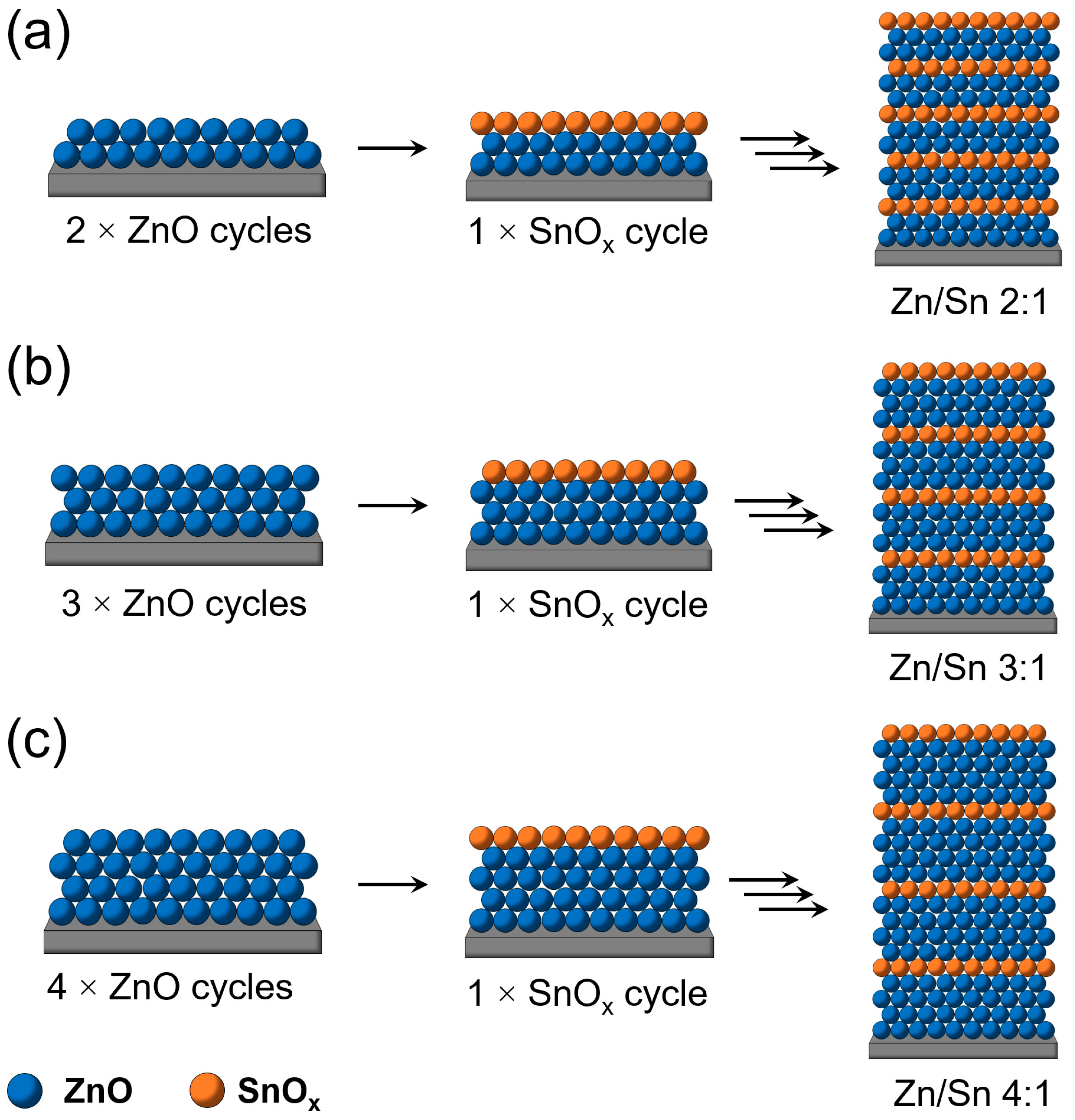
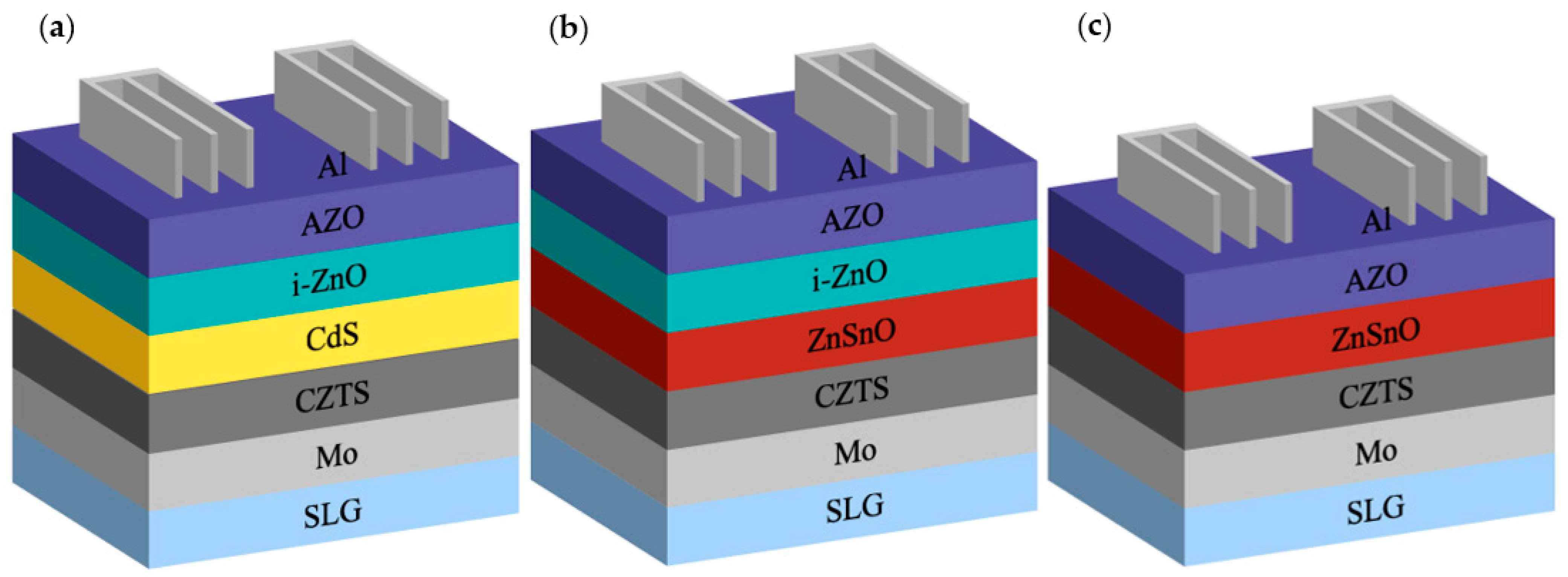
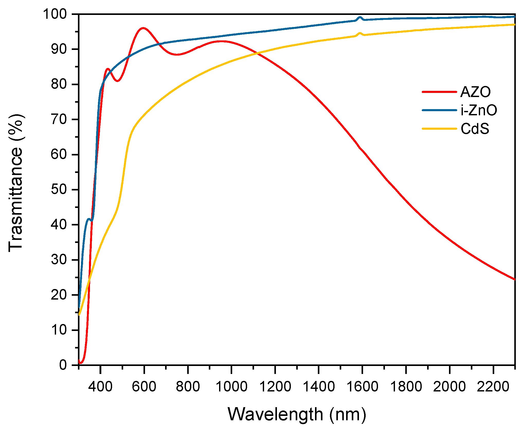
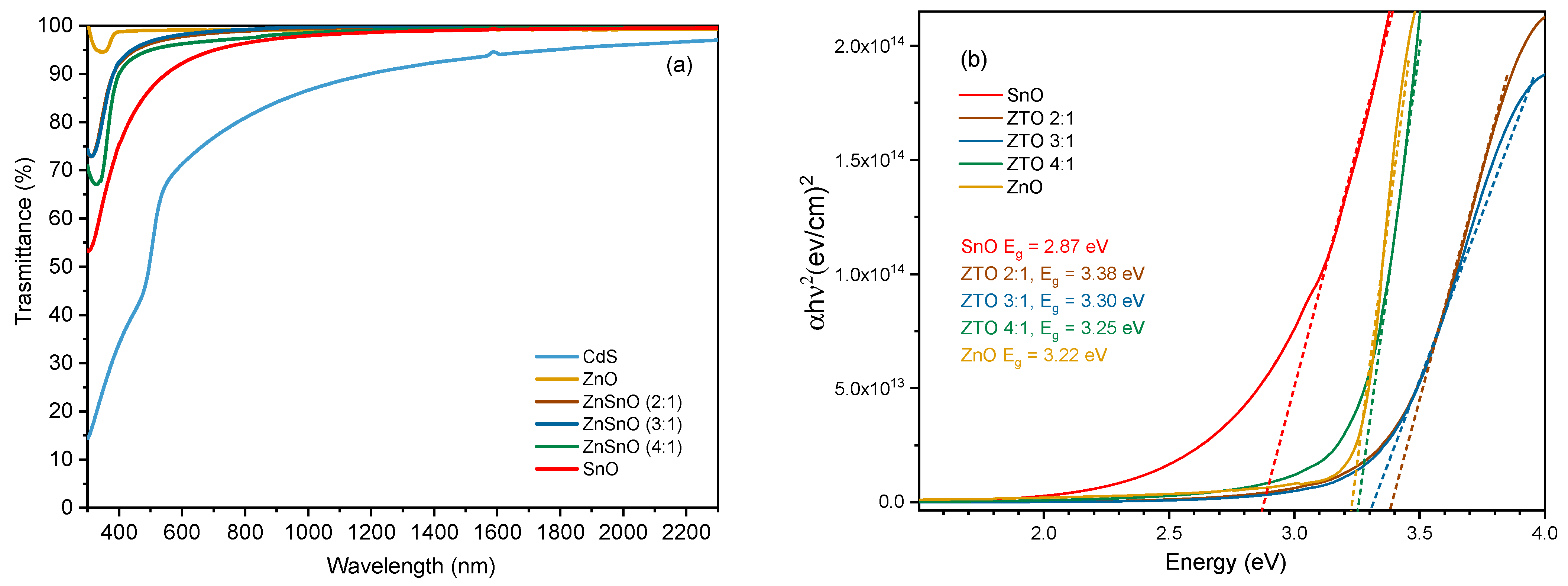
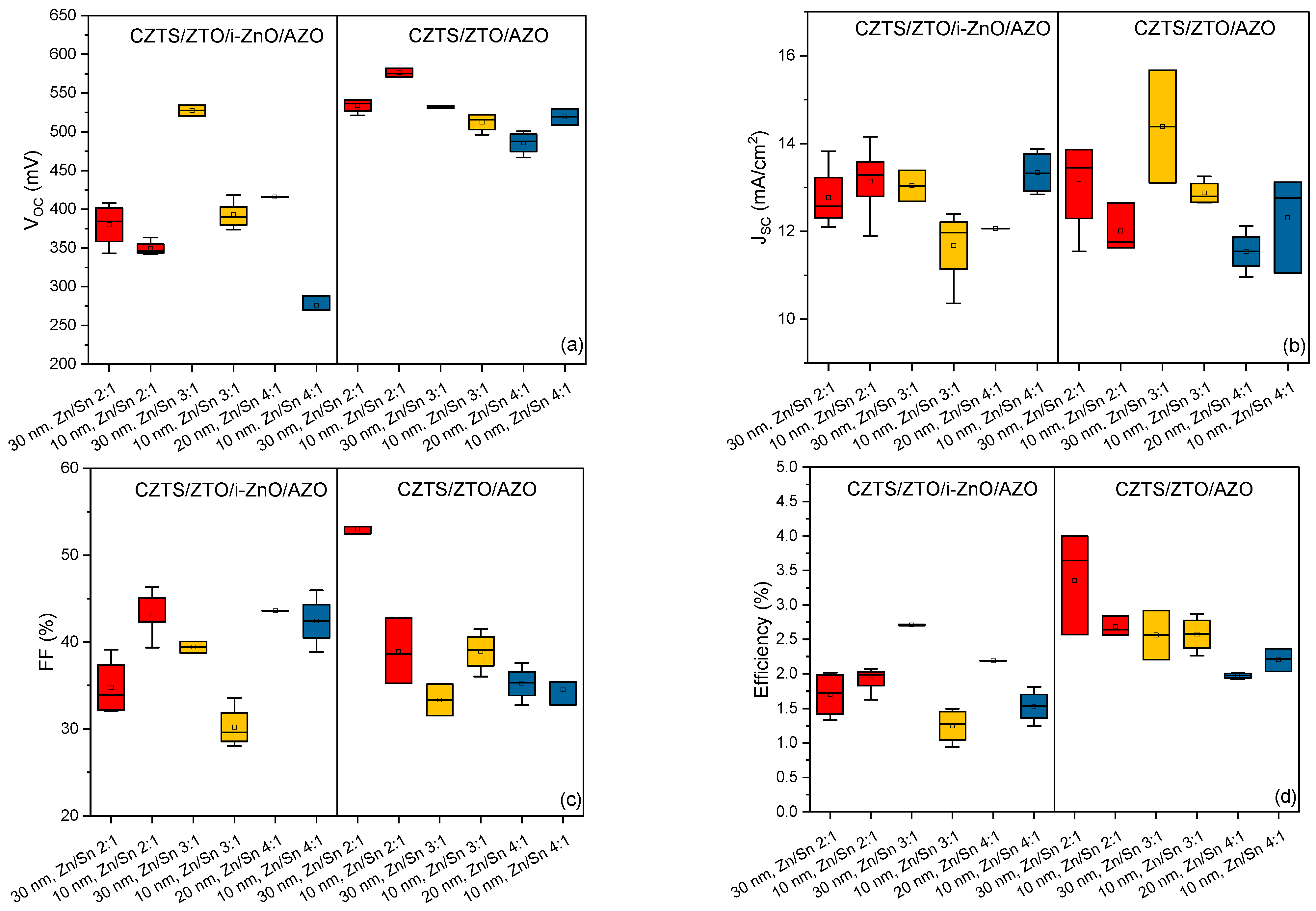
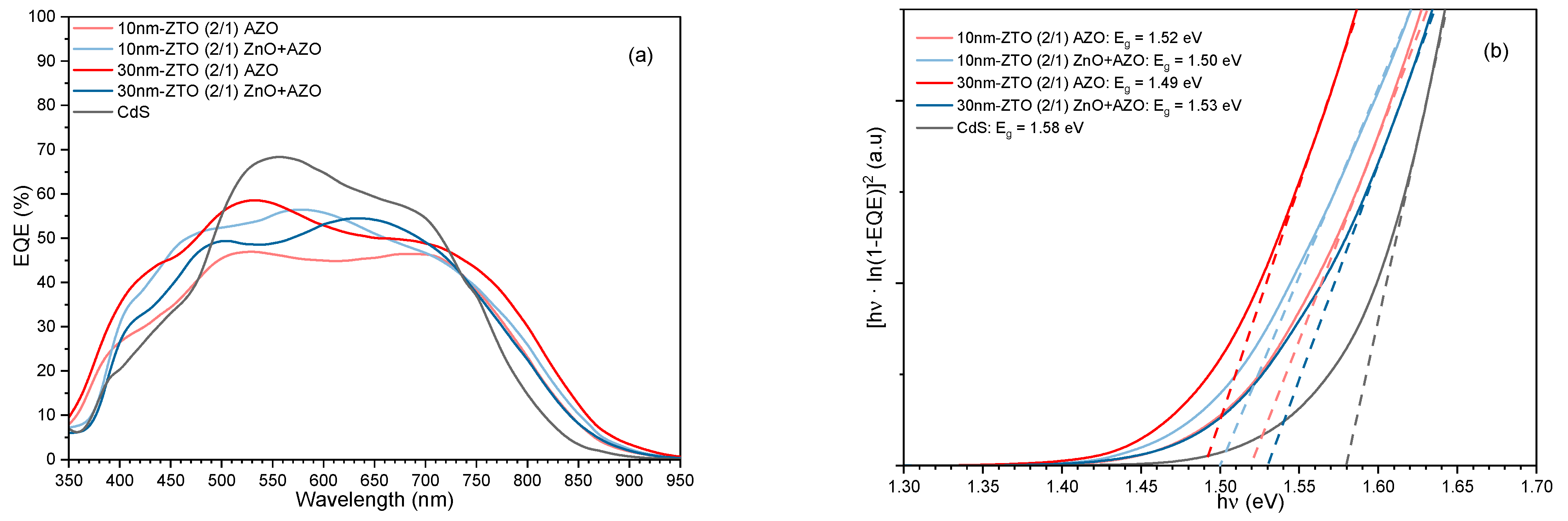
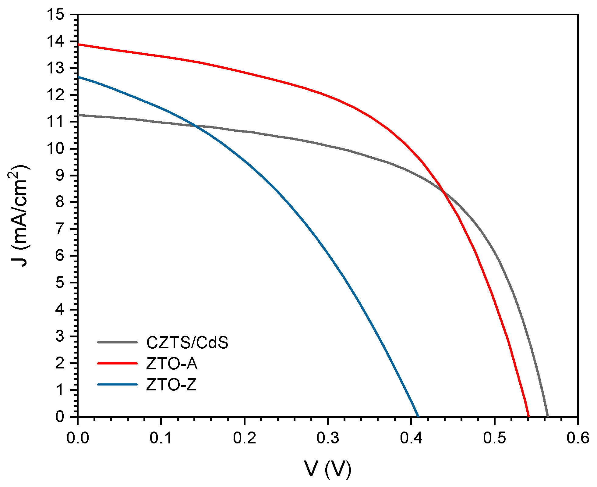
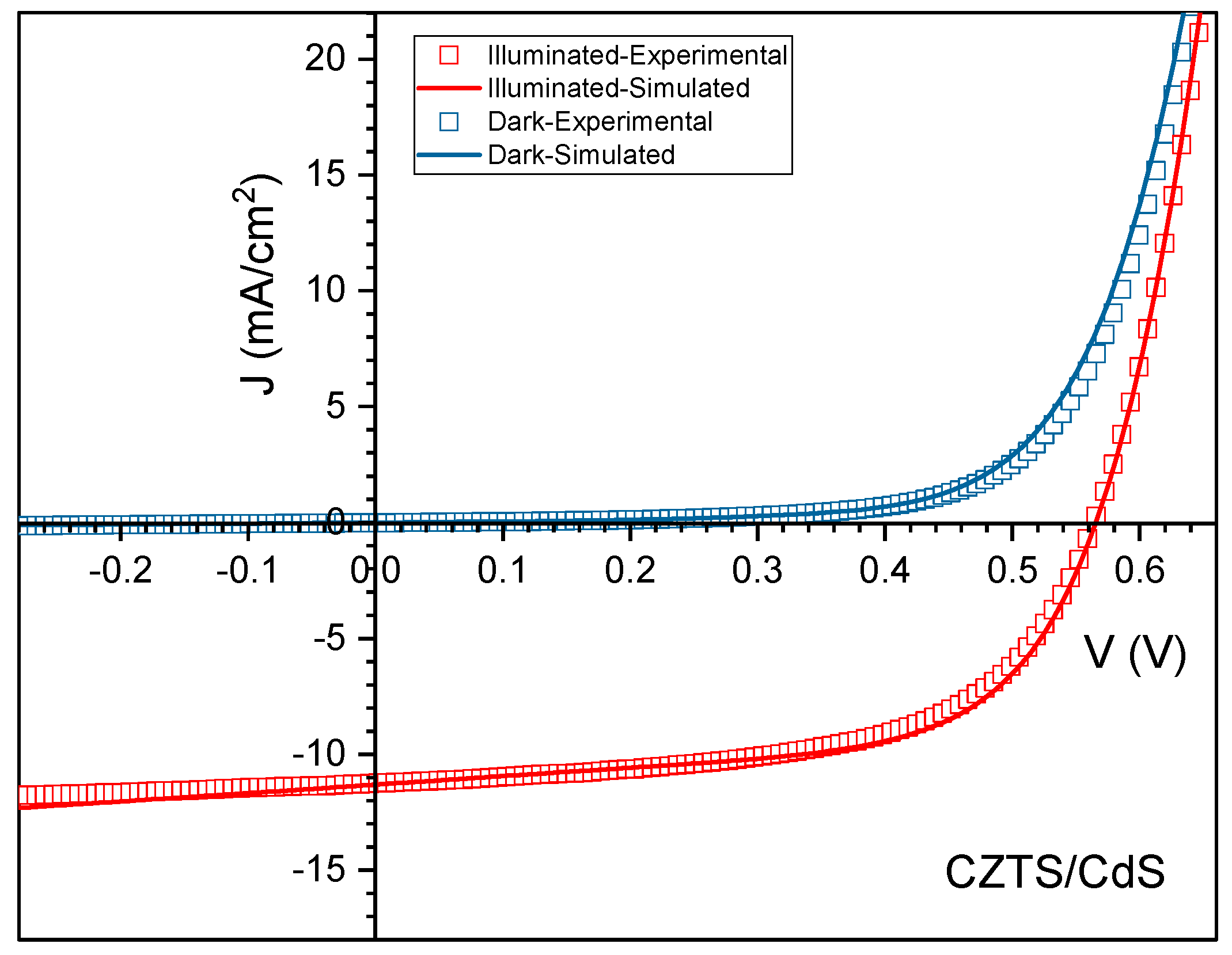
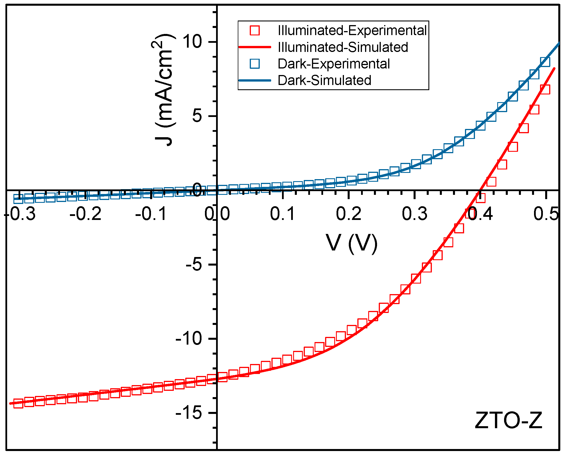
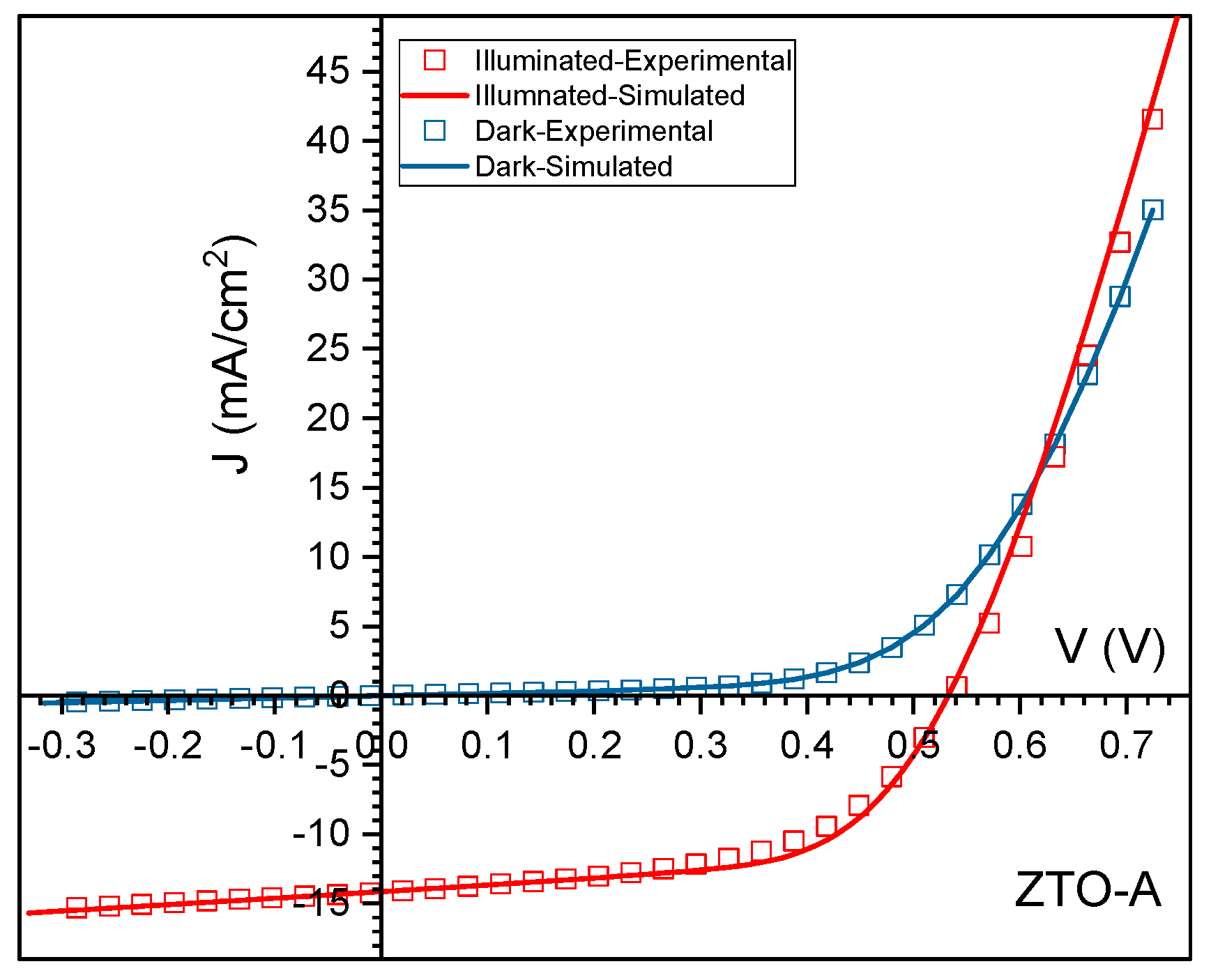
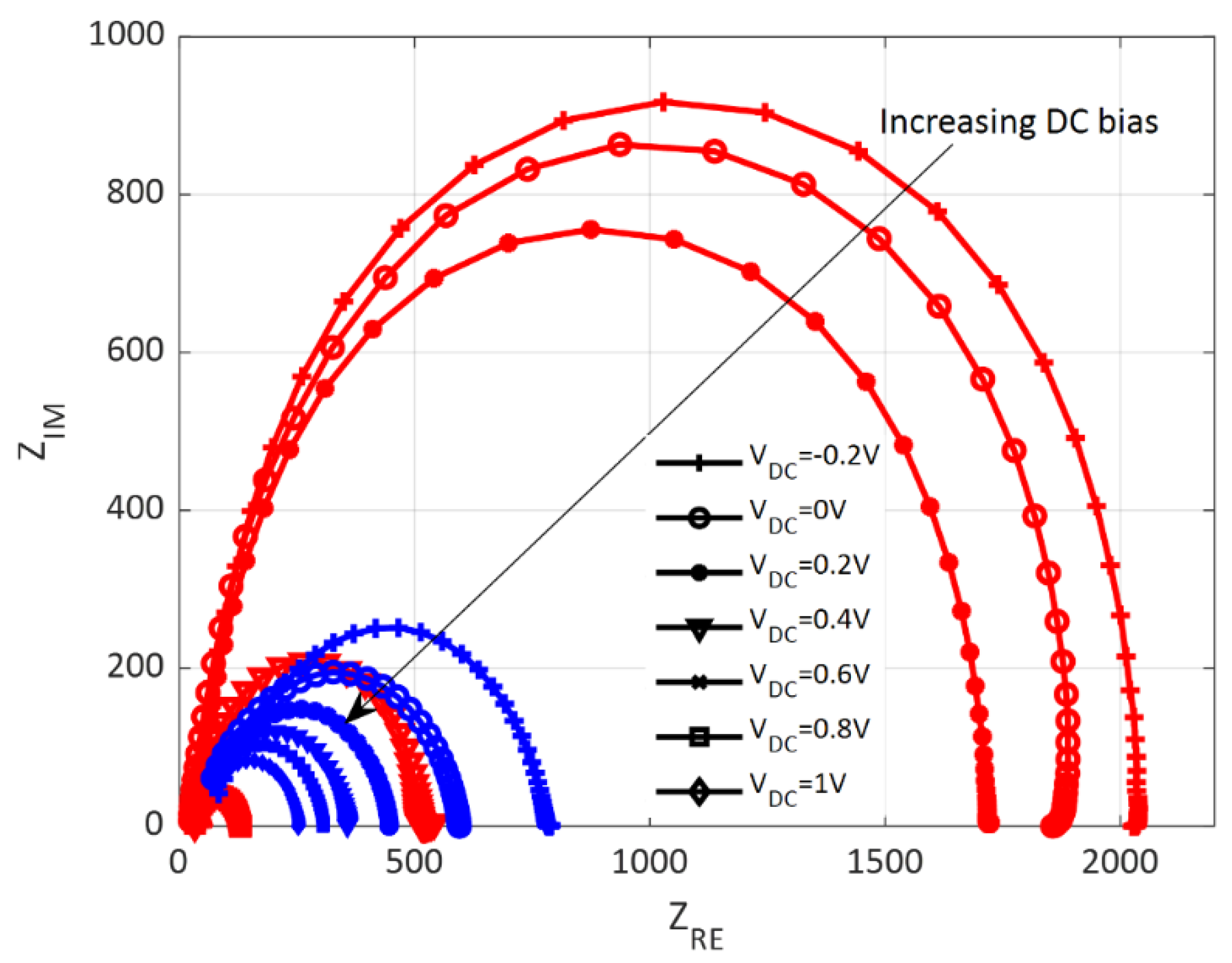
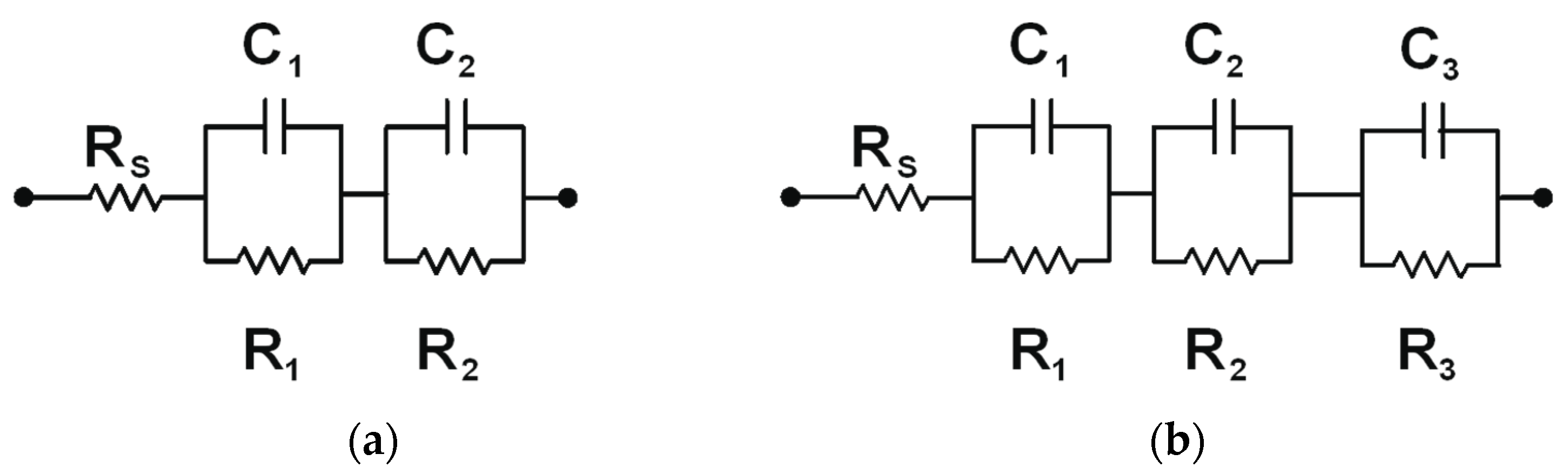
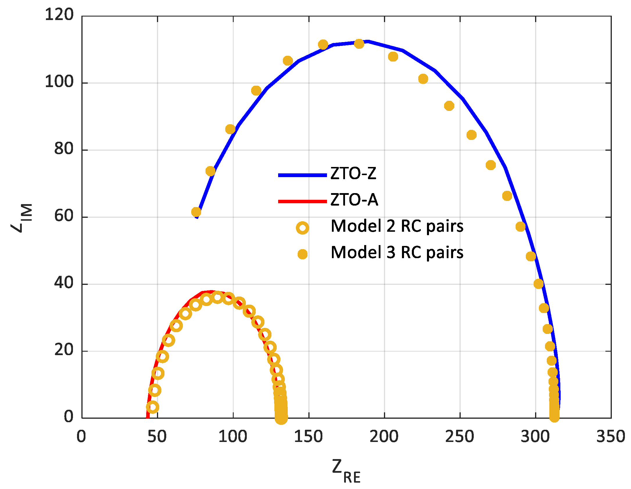
3. Results and Discussion

Based on the recent works reported in the literature, where different compositions of ZnxSn1−xO were tested, the ideal ZTO thin film presents an excess of zinc over the tin. In particular, the most promising Zn/Sn ratios are Zn0.66Sn0.33O, Zn0.75Sn0.25O, and Zn0.8Sn0.2O [19,20,21]. However, the recommended thickness is not unique and varies between 10 and 40 nm. Based on the data in previous reports [17,20], our deposition procedure was optimized, and the precursors to be used were chosen as reported in the previous section. The chemical composition of the ZTO buffer layer was modified by modulating the ratio between ZnO and SnOx cycles.
The optical properties of the top contacts (i-ZnO and AZO) of the CdS and the ZTO buffer layers were characterized by UV-Vis spectroscopy. As shown in Figure 3, CdS, used in the control device (with CZTS/CdS p-n junction), is the material with the highest absorption in the visible range, confirming how replacing this layer with a more transparent material would allow solar radiation to be collected more efficiently.
The same measurements were made on the ZTO films with the three Zn/Sn cycles ratio mentioned above, and then, also ZnO and SnOx binary metal oxides were measured for comparison purposes: the results are shown in Figure 4a. All these samples have greater transparency than CdS in the visible region. Transmittance measurements were also collected to calculate the absorption coefficient and, by applying the Tauc relation, to evaluate the optical band gap [30]. Tauc’s plot of the three ZTO layers and ZnO and SnOx are reported in Figure 4b, with a band gap ranging between 3.2 and 3.4 eV for ZTO. As expected, the band gap shows a non-monotonic variation as a function of the Zn/Sn ratios in agreement with the data reported in the literature [20,21,31,32].
ZTO deposition was performed on the CZTS absorber layer and simultaneously on silicon substrates to assess the ZTO thickness by spectroscopic ellipsometry (SE) and the composition of the so-deposited ZnxSn1−xO films via EDX measurements. Table 1 reports the evaluated compositions of the ZTO thin films with Zn/Sn 2:1, 3:1, and 4:1, showing thicknesses of 34 nm, 29 nm, and 20 nm, respectively.
To evaluate the impact of ZTO thickness on CZTS solar cells performances, it was performed a second sample series to obtain ZTO thicknesses of ~10 nm. A set of CZTS solar cells was then produced to evaluate the performance of the ZTO buffer layer deposited via ALD with different thicknesses (from 10 to ~30 nm). These devices were compared to the ones with the standard architecture Mo/CZTS/CdS/i-ZnO/AZO used as reference. The average device efficiency of the so obtained CZTS/CdS solar cells is around η ≈ 3.9%, with Voc ≈ 560 mV, Jsc ≈ 12 mA/cm2, and FF ≈ 58%.
Regarding ZTO buffer devices, both Mo/CZTS/ZTO/i-ZnO/AZO/Al and Mo/CZTS/ZTO/AZO/Al architectures have been developed to investigate charge extraction. In both structures, layers of ZnxSn1-xO with three different compositions (Zn/Sn = 2:1, 3:1, 4:1) and with two different thicknesses (~30 nm and 10 nm) were analyzed. Table 2 summarizes the characteristics of the as-deposited ALD-ZTO buffer layers together with the PV parameters of the champion devices.
Figure 5 depicts the average values of the PV parameters of all the devices and both architectures and thicknesses. Taking into consideration the open circuit voltage, a dependence of the Voc on the buffer layer composition is observed. Regarding ZTO composition, the best Voc values correspond to Zn/Sn ratio 2:1, with values of 541 mV and 571 mV, for ZTO with ~30 nm and 10 nm, respectively. Regarding the Jsc, the values are fairly constant, regardless of the ZTO composition, ranging between 12 mA/cm2 and 14 mA/cm2. The most interesting results are the ones concerning the fill factor, as they give information about the junction quality. When both the i-ZnO layer and AZO were employed, no trend could be observed. Instead, when the interlayer of i-ZnO is not used, higher FFs are achieved. On the other hand, the best FFs results (between 51% and 53%) and the highest efficiencies (between 2.6% and 4.0%) were achieved with a buffer layer with Zn/Sn ratio 2:1, with ZTO 30 nm thick and without the i-ZnO layer in the device structure. Comparing the CZTS/ZTO/AZO devices with CZTS/CdS/i-ZnO/AZO control devices (Table 2, Entry #1 and Entry #8), it is possible to observe similar efficiency.
External quantum efficiency measurements were performed to study the spectral response of the devices employing ZTO with Zn/Sn ratio 2:1 as the buffer layer, which achieved the highest efficiencies (Figure 6a), and to compare them with the control device (CZTS/CdS junction). The EQE gain of removing the i-ZnO layer is already clear in the first range of interest (350 nm–400 nm), where typically, the i-ZnO and AZO have their parasitic absorption [33]. The control device’s EQE reduction between 350 nm and 470 nm is mainly due to the CdS layer; then, this parasitic absorption is removed by replacing the CdS with the ZTO. The only wavelength range in which ZTO is less effective than CdS is the region between 500 nm and 700 nm, which is more affected by light reflection [20]. In this case, the introduction of an antireflective coating could be beneficial and increase the gain in this area as well, as already reported for the ZTO-based devices [34]. Finally, in the spectral region between 750 and 950 nm, the ZTO layer allows for better charge extraction, probably due to the reduced recombination of charge carriers [33]. Figure 6b shows the evaluated electronic bandgap [35]. The values calculated from the EQE data are affected by the recombination losses and by the functional layers employed in the device architecture [33]: the device showing an electronic bandgap closer to the expected value (1.50 eV) is the 30nm-ZTO (2/1) AZO. From EQE data, it can be deduced that the most efficient device configuration is the one with ZTO (Zn/Sn ratio 2:1) with 30 nm thickness and no i-ZnO, as confirmed by the J–V curves (Figure 7). This results in lower use of materials and the removal of a process step for the manufacture of photovoltaic devices, thus leading to a reduction in time, costs and energy required to produce CZTS PV devices.
The J–V curves of the record devices with the CZTS/ZTO heterojunction (ZTO = 30 nm with Zn/Sn = 2:1) are shown in Figure 7, and they are compared to the ones of the control device with the CZTS/CdS heterojunction. SCAPS-1D simulations and IS measurements have been performed on CZTS/ZTO/i-ZnO/AZO and CZTS/ZTO/AZO devices, from now on called, respectively, ZTO-Z and ZTO-A, to evaluate the differences of charge extraction depending on the presence of i-ZnO layer.
The numerical simulation of CZTS solar cells using SCAPS-1D version 3.3.08 [36] was carried out to study the alternative buffer layer ZTO and the device architecture’s impact on the overall CZTS solar cell device performances. Output parameters such as J–V characteristics under illumination can be extrapolated from the results obtained from the simulations. Solar Cell Capacitance Simulator (SCAPS-1D) is one-dimensional solar cell simulation software developed at the Department of Electronics and Information Systems (ELIS) of the University of Gent in Belgium and used for numerical analysis of solar cells. Several profiles, such as grading, generation, recombination, and defects (in bulk and at the interfaces), can be calculated for a given device architecture. The default temperature was set at 300 K with standard illumination of AM1.5G, as defined by the global reference spectrum for flat-plate devices, listed in standards IEC 60904–3 edition 2 and ASTM G173–03 [5].
The material parameters used in the simulation, listed in Table 3, Table 4 and Table 5, were all carefully chosen from experimental studies and modeling works that have been performed with SCAPS and already reported in the literature [37,38,39,40,41,42,43,44,45,46].
The shunt and series resistances, obtained by a pre-fitting procedure carried out using an ad-hoc program written in Matlab ambient (software version 9.13.0 R2022b) [47], have been introduced for all solar cells as fixed parameters. These values were refined during the simulation process but without a significant deviation from those obtained by the pre-fitting and are all reported in Table 6.
Figure 8 reports the simulation results for the J–V curves (dark and light) for the control device with CZTS/CdS junction. Starting from this simulation, the CdS was removed in the SCAPS simulated structure, and the ZTO film was then introduced, initially keeping the i-ZnO layer in the device architecture (ZTO-Z device). Then, the i-ZnO layer was removed to model the ZTO-A device. The resulting simulations are reported in Figure 9 and Figure 10, respectively.
The recombination center density was adjusted at the CZTS/ZTO interface while the remaining parameters were kept fixed (except for the resistances) to fit the model to the ZTO-A device data. On the other hand, for the ZTO-Z device, a reliable simulation was achieved considering that the ZTO film changes its characteristics near the interface with i-ZnO, presenting properties in the electron affinity and bandgap close to the ones of the i-ZnO layer. It can be assumed that the conditions used for the i-ZnO sputtering deposition can alter the ZTO nature and properties leading to a sole intermixed layer with features more like i-ZnO than ZTO instead of a stack of the two. The RF Magnetron sputtering employed here involves a mixture of Ar/O2 plasma necessary to compensate for oxygen losses during the i-ZnO deposition, and this feature could also alter the ZTO stoichiometry. This assumption can be made according to Haddout and coworkers [39], reporting a deterioration in PV device performance in the case of ZTO films with characteristics (electronic affinity and band gap) approaching those of pure ZnO or SnO films. This hypothesis can give a reliable explanation for the worse performances of the ZTO-Z device compared to ZTO-A. Moreover, it has to be considered that the i-ZnO layer was usually employed to face issues related to possible shunts given by a certain surface inhomogeneity typical of a chemical bath deposition [48]. ALD, for definition, leads to compact layers [49], so the i-ZnO sputtered layer is formally redundant and, at least in this case, detrimental.
IS measurements have been performed on ZTO-A and ZTO-Z devices to demonstrate this hypothesis. IS is a powerful characterization technique that allows the investigation of the physics taking place at the various interfaces existing in the device by only accessing its external terminals [50]. This technique has been widely employed in the study of semiconductor devices, with special emphasis on solar cells [51,52,53,54,55]. Impedance data are usually shown in the form of a Nyquist plot. Such graphs represent the real part of the measured impedance on the x-axis and the imaginary part on the y-axis. Each curve is obtained for a given DC bias (VDC), while each point on the curve is measured for a specific frequency. These plots are usually chosen since it is possible to readily extract the equivalent circuit configuration from such form. Nyquist plots that exhibit a semicircular shape can be described with an equivalent circuit composed of a single RC pair (the parallel connection of a Resistor and a Capacitor), while the shift on the x-axis is represented by a series resistance in the equivalent configuration [56]. The resulting Nyquist plots for ZTO-A (red lines) and ZTO-Z (blue lines) samples are shown in Figure 11, where it is possible to notice that the AC behavior of the two devices is significantly different.
The radius of the Nyquist plots associated with the ZTO-A is initially very large, while it reduces exponentially with increasing imposed VDC, as expected. This trend is not visible in the case of the ZTO-Z device, where the radius of the Nyquist plots decreases almost linearly with applied bias. Since, in both cases, the Nyquist plots do not show a semicircular shape, the equivalent circuit cannot include a single RC pair. Thus, an automatic procedure allowing the extraction of the equivalent circuit from the impedance spectra has been performed [56]. The extracted circuit represents the configuration describing the AC behavior with the minimum error with respect to the measured data. The selected circuits for the ZTO-A and ZTO-Z devices are presented, respectively, in Figure 12a,b. The extracted equivalent circuit for ZTO-A and ZTO-Z is composed, respectively, of two RC pairs and three RC pairs. Thus, the introduction of an additional resistive layer, such as i-ZnO, results in the occurrence of a third RC pair.
Nyquist plots obtained from the extracted circuit model, in both cases, are comparable with experimental data. In particular, the comparison between the model and experimental data for a VDC equal to the open circuit voltage is shown in Figure 13, where it can be noticed that the extracted configurations are suitable to model the AC behavior of both samples.
Based on these results, we can confirm that when the ZTO buffer layer is deposited through ALD, then the i-ZnO layer is not only not necessary but, at least in our case, also detrimental to the charge extraction, limiting the solar cell behavior due to its resistive nature.

4. Conclusions

In conclusion, we report on our optimized process to produce efficient Cd-free kesterite solar cells featuring ZnxSn1-xO as a buffer layer deposited via ALD. We found the best Zn/Sn ratio being 2:1 and the optimal thickness being 30 nm. We experimentally confirmed that ZTO is a good alternative to CdS as a buffer layer in CZTS solar cells, leading to efficiencies of η = 4%, comparable and even slightly higher than our CZTS/CdS control device (η = 3.9%), using the simplest device architecture Mo/CZTS/ZTO/AZO/Al.
Compared to other experimental works reported on this topic, we investigated through SCAPS simulations and IS measurements on the charge extraction of the final devices, proving that the top layers of the solar cell strongly impact the PV performance. Specifically, the i-ZnO window layer is conventionally used to prevent shunts in cells with CZTS/CdS junction due to the uneven growth of CdS during the chemical bath deposition. In this case, when ZTO is deposited through ALD, the i-ZnO window layer is not only redundant but also detrimental to the charge extraction due to its resistive nature.
All evidence suggests that, by using our optimized ALD-ZTO synthesis with the simplest possible solar cell architecture (Mo/CZTS/ZTO/AZO/Al), ZTO could be regularly used as a buffer layer in highly efficient, Cd-free CZTS solar cells.

Author Contributions

Conceptualization, G.T. and V.D.P.; methodology, V.D.P., M.V. and C.M.; investigation, G.T. and V.D.P.; data curation, C.G., V.T., M.A. and I.M.; writing original draft preparation, C.G., V.T., V.D.P., I.M. and M.A.; writing review and editing, G.T., C.G., V.T. V.D.P., M.V., C.M., I.M. and M.A.; visualization, C.G.; supervision, S.B. and S.D.; project administration, S.B.; funding acquisition, S.B. All authors have read and agreed to the published version of the manuscript.

Funding

This work was supported by the Italian Ministry of Economic Development in the framework of the Operating Agreement with ENEA for Research on the Electric System. The authors also acknowledge the University of Milano-Bicocca for funding through “Bando Infrastrutture di Ricerca 2021” and the project PON named “Bifacial Efficient Solar Cell Technology with 4-Terminal Architecture for Utility Scale” called “BEST-4U”, financed by the Italian Ministry MIUR (CUPB88D19000160005).

Data Availability Statement

The data presented in this work are available on request from the corresponding authors.

Conflicts of Interest

The authors declare no conflict of interest.

References

  1. Liu, F.; Zeng, Q.; Li, J.; Hao, X.; Ho-Baillie, A.; Tang, J.; Green, M.A. Emerging Inorganic Compound Thin Film Photovoltaic Materials: Progress, Challenges and Strategies. Mater. Today 2020, 41, 120–142. [Google Scholar] [CrossRef]
  2. He, M.; Yan, C.; Li, J.; Suryawanshi, M.P.; Kim, J.; Green, M.A.; Hao, X. Kesterite Solar Cells: Insights into Current Strategies and Challenges. Adv. Sci. 2021, 8, 2004313. [Google Scholar] [CrossRef] [PubMed]
  3. Valentini, M.; Malerba, C.; Menchini, F.; Tedeschi, D.; Polimeni, A.; Capizzi, M.; Mittiga, A. Effect of the Order-Disorder Transition on the Optical Properties of Cu2ZnSnS4. Appl. Phys. Lett. 2016, 108, 211909. [Google Scholar] [CrossRef]
  4. Giraldo, S.; Jehl, Z.; Placidi, M.; Izquierdo-Roca, V.; Pérez-Rodríguez, A.; Saucedo, E. Progress and Perspectives of Thin Film Kesterite Photovoltaic Technology: A Critical Review. Adv. Mater. 2019, 31, 1806692. [Google Scholar] [CrossRef] [PubMed]
  5. Green, M.A.; Dunlop, E.D.; Hohl-Ebinger, J.; Yoshita, M.; Kopidakis, N.; Bothe, K.; Hinken, D.; Rauer, M.; Hao, X. Solar Cell Efficiency Tables (Version 60). Prog. Photovolt. Res. Appl. 2022, 30, 687–701. [Google Scholar] [CrossRef]
  6. Islam, M.F.; Md Yatim, N.; Hashim Ismail, M.A. A Review of CZTS Thin Film Solar Cell Technology. J. Adv. Res. Fluid Mech. Therm. Sci. 2021, 81, 73–87. [Google Scholar] [CrossRef]
  7. Pal, K.; Singh, P.; Bhaduri, A.; Thapa, K.B. Current Challenges and Future Prospects for a Highly Efficient (>20%) Kesterite CZTS Solar Cell: A Review. Sol. Energy Mater. Sol. Cells 2019, 196, 138–156. [Google Scholar] [CrossRef]
  8. Bär, M.; Schubert, B.-A.; Marsen, B.; Wilks, R.G.; Pookpanratana, S.; Blum, M.; Krause, S.; Unold, T.; Yang, W.; Weinhardt, L.; et al. Cliff-like Conduction Band Offset and KCN-Induced Recombination Barrier Enhancement at the CdS/Cu2ZnSnS4 Thin-Film Solar Cell Heterojunction. Appl. Phys. Lett. 2011, 99, 222105. [Google Scholar] [CrossRef]
  9. Haight, R.; Barkhouse, A.; Gunawan, O.; Shin, B.; Copel, M.; Hopstaken, M.; Mitzi, D.B. Band Alignment at the Cu2ZnSn(SxSe1−x)4/CdS Interface. Appl. Phys. Lett. 2011, 98, 253502. [Google Scholar] [CrossRef]
  10. Yan, C.; Liu, F.; Song, N.; Ng, B.K.; Stride, J.A.; Tadich, A.; Hao, X. Band Alignments of Different Buffer Layers (CdS, Zn(O,S), and In2S3) on Cu2ZnSnS4. Appl. Phys. Lett. 2014, 104, 173901. [Google Scholar] [CrossRef]
  11. Courel, M.; Andrade-Arvizu, J.A.; Vigil-Galán, O. Towards a CdS/Cu2ZnSnS4 Solar Cell Efficiency Improvement: A Theoretical Approach. Appl. Phys. Lett. 2014, 105, 233501. [Google Scholar] [CrossRef]
  12. Santoni, A.; Biccari, F.; Malerba, C.; Valentini, M.; Chierchia, R.; Mittiga, A. Valence Band Offset at the CdS/Cu2ZnSnS4 Interface Probed by x-Ray Photoelectron Spectroscopy. J. Phys. D Appl. Phys. 2013, 46, 175101. [Google Scholar] [CrossRef]
  13. Nugroho, H.S.; Refantero, G.; Septiani, N.L.W.; Iqbal, M.; Marno, S.; Abdullah, H.; Prima, E.C.; Nugraha; Yuliarto, B. A Progress Review on the Modification of CZTS(e)-Based Thin-Film Solar Cells. J. Ind. Eng. Chem. 2022, 105, 83–110. [Google Scholar] [CrossRef]
  14. Lin, L.-Y.; Qiu, Y.; Zhang, Y.; Zhang, H. Analysis of Effect of Zn(O,S) Buffer Layer Properties on CZTS Solar Cell Performance Using AMPS. Chin. Phys. Lett. 2016, 33, 107801. [Google Scholar] [CrossRef]
  15. Tseberlidis, G.; Di Palma, V.; Trifiletti, V.; Frioni, L.; Valentini, M.; Malerba, C.; Mittiga, A.; Acciarri, M.; Binetti, S.O. Titania as Buffer Layer for Cd-Free Kesterite Solar Cells. ACS Mater. Lett. 2023, 5, 219–224. [Google Scholar] [CrossRef] [PubMed]
  16. Seo, J.; Yoo, H. Zinc–Tin Oxide Film as an Earth-Abundant Material and Its Versatile Applications to Electronic and Energy Materials. Membranes 2022, 12, 485. [Google Scholar] [CrossRef]
  17. Cho, J.Y.; Jang, J.S.; Karade, V.C.; Nandi, R.; Pawar, P.S.; Seok, T.-J.; Moon, W.; Park, T.J.; Kim, J.H.; Heo, J. Atomic-Layer-Deposited ZnSnO Buffer Layers for Kesterite Solar Cells: Impact of Zn/(Zn+Sn) Ratio on Device Performance. J. Alloy. Compd. 2022, 895, 162651. [Google Scholar] [CrossRef]
  18. Hultqvist, A.; Platzer-Björkman, C.; Zimmermann, U.; Edoff, M.; Törndahl, T. Growth Kinetics, Properties, Performance, and Stability of Atomic Layer Deposition Zn–Sn–O Buffer Layers for Cu(In,Ga)Se2 Solar Cells. Prog. Photovolt. Res. Appl. 2012, 20, 883–891. [Google Scholar] [CrossRef]
  19. Lindahl, J.; Wätjen, J.T.; Hultqvist, A.; Ericson, T.; Edoff, M.; Törndahl, T. The Effect of Zn1−xSnxOy Buffer Layer Thickness in 18.0% Efficient Cd-Free Cu(In,Ga)Se2 Solar Cells. Prog. Photovolt. Res. Appl. 2013, 21, 1588–1597. [Google Scholar] [CrossRef]
  20. Cui, X.; Sun, K.; Huang, J.; Lee, C.-Y.; Yan, C.; Sun, H.; Zhang, Y.; Liu, F.; Hossain, M.A.; Zakaria, Y.; et al. Enhanced Heterojunction Interface Quality to Achieve 9.3% Efficient Cd-Free Cu2ZnSnS4 Solar Cells Using Atomic Layer Deposition ZnSnO Buffer Layer. Chem. Mater. 2018, 30, 7860–7871. [Google Scholar] [CrossRef]
  21. Li, X.; Su, Z.; Venkataraj, S.; Batabyal, S.K.; Wong, L.H. 8.6% Efficiency CZTSSe Solar Cell with Atomic Layer Deposited Zn-Sn-O Buffer Layer. Sol. Energy Mater. Sol. Cells 2016, 157, 101–107. [Google Scholar] [CrossRef]
  22. Ericson, T.; Larsson, F.; Törndahl, T.; Frisk, C.; Larsen, J.; Kosyak, V.; Hägglund, C.; Li, S.; Platzer-Björkman, C. Zinc-Tin-Oxide Buffer Layer and Low Temperature Post Annealing Resulting in a 9.0% Efficient Cd-Free Cu2ZnSnS4 Solar Cell. Sol. RRL 2017, 1, 1700001. [Google Scholar] [CrossRef]
  23. Lee, J.; Enkhbat, T.; Han, G.; Sharif, M.H.; Enkhbayar, E.; Yoo, H.; Kim, J.H.; Kim, S.; Kim, J. Over 11 % Efficient Eco-Friendly Kesterite Solar Cell: Effects of S-Enriched Surface of Cu2ZnSn(S,Se)4 Absorber and Band Gap Controlled (Zn,Sn)O Buffer. Nano Energy 2020, 78, 105206. [Google Scholar] [CrossRef]
  24. Larsen, J.K.; Larsson, F.; Törndahl, T.; Saini, N.; Riekehr, L.; Ren, Y.; Biswal, A.; Hauschild, D.; Weinhardt, L.; Heske, C.; et al. Cadmium Free Cu2ZnSnS4 Solar Cells with 9.7% Efficiency. Adv. Energy Mater. 2019, 9, 1900439. [Google Scholar] [CrossRef]
  25. Cui, X.; Sun, K.; Huang, J.; Yun, J.S.; Lee, C.-Y.; Yan, C.; Sun, H.; Zhang, Y.; Xue, C.; Eder, K.; et al. Cd-Free Cu2ZnSnS4 Solar Cell with an Efficiency Greater than 10% Enabled by Al2O3 Passivation Layers. Energy Env. Sci. 2019, 12, 2751–2764. [Google Scholar] [CrossRef]
  26. Grenet, L.; Emieux, F.; Andrade-Arvizu, J.; De Vito, E.; Lorin, G.; Sánchez, Y.; Saucedo, E.; Roux, F. Sputtered ZnSnO Buffer Layers for Kesterite Solar Cells. ACS Appl. Energy. Mater. 2020, 3, 1883–1891. [Google Scholar] [CrossRef]
  27. Malerba, C.; Valentini, M.; Mittiga, A. Cation Disorder in Cu2ZnSnS4 Thin Films: Effect On Solar Cell Performances. Sol. RRL 2017, 1, 1700101. [Google Scholar] [CrossRef]
  28. Yan, C.; Huang, J.; Sun, K.; Johnston, S.; Zhang, Y.; Sun, H.; Pu, A.; He, M.; Liu, F.; Eder, K.; et al. Cu2ZnSnS4 Solar Cells with over 10% Power Conversion Efficiency Enabled by Heterojunction Heat Treatment. Nat. Energy 2018, 3, 764–772. [Google Scholar] [CrossRef]
  29. Tauc, J.; Grigorovici, R.; Vancu, A. Optical Properties and Electronic Structure of Amorphous Germanium. Phys. Status Solidi B 1966, 15, 627–637. [Google Scholar] [CrossRef]
  30. Tauc, J.; Menth, A. States in the Gap. J. Non. Cryst. Solids. 1972, 8–10, 569–585. [Google Scholar] [CrossRef]
  31. Kahouli, M.; Barhoumi, A.; Bouzid, A.; Al-Hajry, A.; Guermazi, S. Structural and Optical Properties of ZnO Nanoparticles Prepared by Direct Precipitation Method. Superlattices Microstruct. 2015, 85, 7–23. [Google Scholar] [CrossRef]
  32. Zhou, W.; Umezawa, N. Band Gap Engineering of Bulk and Nanosheet SnO: An Insight into the Interlayer Sn–Sn Lone Pair Interactions. Phys. Chem. Chem. Phys. 2015, 17, 17816–17820. [Google Scholar] [CrossRef] [PubMed]
  33. Nakane, A.; Tampo, H.; Tamakoshi, M.; Fujimoto, S.; Kim, K.M.; Kim, S.; Shibata, H.; Niki, S.; Fujiwara, H. Quantitative Determination of Optical and Recombination Losses in Thin-Film Photovoltaic Devices Based on External Quantum Efficiency Analysis. J. Appl. Phys. 2016, 120, 064505. [Google Scholar] [CrossRef]
  34. Mirzaei, M.; Hasanzadeh, J.; Abdolahzadeh Ziabari, A. Significant Efficiency Enhancement in Ultrathin CZTS Solar Cells by Combining Al Plasmonic Nanostructures Array and Antireflective Coatings. Plasmonics 2021, 16, 1375–1390. [Google Scholar] [CrossRef]
  35. Zoppi, G.; Forbes, I.; Miles, R.W.; Dale, P.J.; Scragg, J.J.; Peter, L.M. Cu2ZnSnSe4 Thin Film Solar Cells Produced by Selenisation of Magnetron Sputtered Precursors. Prog. Photovolt. Res. Appl. 2009, 17, 315–319. [Google Scholar] [CrossRef]
  36. Burgelman, M.; Decock, K.; Niemegeers, A.; Verschraegen, J.; Degrave, S. SCAPS Manual; University of Gent: Gent, Belgium, 2021. [Google Scholar]
  37. Ashraf, M.A.; Alam, I. Numerical Simulation of CIGS, CISSe and CZTS-Based Solar Cells with In2S3 as Buffer Layer and Au as Back Contact Using SCAPS 1D. Eng. Res. Express 2020, 2, 035015. [Google Scholar] [CrossRef]
  38. Kumar, A.; Thakur, A.D. Role of Contact Work Function, Back Surface Field, and Conduction Band Offset in Cu2ZnSnS4 Solar Cell. Jpn. J. Appl. Phys. 2018, 57, 08RC05. [Google Scholar] [CrossRef]
  39. Haddout, A.; Fahoume, M.; Raidou, A.; Lharch, M. Numerical Modeling of ZnSnO/CZTS Based Solar Cells. Optoelectron. Lett. 2022, 18, 276–282. [Google Scholar] [CrossRef]
  40. Haddout, A.; Fahoume, M.; Qachaou, A.; Raidou, A.; Lharch, M. Understanding Effects of Defects in Bulk Cu2ZnSnS4 Absorber Layer of Kesterite Solar Cells. Sol. Energy 2020, 211, 301–311. [Google Scholar] [CrossRef]
  41. Enayati Maklavani, S.; Mohammadnejad, S. The Impact of the Carrier Concentration and Recombination Current on the p+pn CZTS Thin Film Solar Cells. Opt. Quantum Electron. 2020, 52, 279. [Google Scholar] [CrossRef]
  42. Bencherif, H.; Dehimi, L.; Mahsar, N.; Kouriche, E.; Pezzimenti, F. Modeling and Optimization of CZTS Kesterite Solar Cells Using TiO2 as Efficient Electron Transport Layer. Mater. Sci. Eng. B 2022, 276, 115574. [Google Scholar] [CrossRef]
  43. Ferdaous, M.T.; Shahahmadi, S.A.; Chelvanathan, P.; Akhtaruzzaman, M.; Alharbi, F.H.; Sopian, K.; Tiong, S.K.; Amin, N. Elucidating the Role of Interfacial MoS2 Layer in Cu2ZnSnS4 Thin Film Solar Cells by Numerical Analysis. Sol. Energy 2019, 178, 162–172. [Google Scholar] [CrossRef]
  44. Belarbi, F.; Rahal, W.; Rached, D.; Benghabrit, S.; Adnane, M. A Comparative Study of Different Buffer Layers for CZTS Solar Cell Using Scaps-1D Simulation Program. Optik 2020, 216, 164743. [Google Scholar] [CrossRef]
  45. Tseberlidis, G.; Trifiletti, V.; Le Donne, A.; Frioni, L.; Acciarri, M.; Binetti, S. Kesterite Solar-Cells by Drop-Casting of Inorganic Sol–Gel Inks. Sol. Energy 2020, 208, 532–538. [Google Scholar] [CrossRef]
  46. Tseberlidis, G.; Hasan Husien, A.; Riva, S.; Frioni, L.; Le Donne, A.; Acciarri, M.; Binetti, S. Semi-Transparent Cu2ZnSnS4 Solar Cells by Drop-Casting of Sol-Gel Ink. Sol. Energy 2021, 224, 134–141. [Google Scholar] [CrossRef]
  47. MATLAB, Version: 9.13.0 (R2022b); The MathWorks, Inc.: Natick, MA, USA, 2022.
  48. Doroody, C.; Rahman, K.S.; Rosly, H.N.; Harif, M.N.; Isah, M.; Kar, Y.B.; Tiong, S.K.; Amin, N. A Comparative Study of CdS Thin Films Grown on Ultra-Thin Glass Substrates by RF Magnetron Sputtering and Chemical Bath Deposition. Mater. Sci. Semicond. Process. 2021, 133, 105935. [Google Scholar] [CrossRef]
  49. Oviroh, P.O.; Akbarzadeh, R.; Pan, D.; Coetzee, R.A.M.; Jen, T.-C. New Development of Atomic Layer Deposition: Processes, Methods and Applications. Sci. Technol. Adv. Mater. 2019, 20, 465–496. [Google Scholar] [CrossRef]
  50. Macdonald, J.R. Impedance Spectroscopy. Ann. Biomed. Eng. 1992, 20, 289–305. [Google Scholar] [CrossRef]
  51. Yadav, P.; Pandey, K.; Bhatt, V.; Kumar, M.; Kim, J. Critical Aspects of Impedance Spectroscopy in Silicon Solar Cell Characterization: A Review. Renew. Sustain. Energy Rev. 2017, 76, 1562–1578. [Google Scholar] [CrossRef]
  52. Sacco, A. Electrochemical Impedance Spectroscopy: Fundamentals and Application in Dye-Sensitized Solar Cells. Renew. Sustain. Energy Rev. 2017, 79, 814–829. [Google Scholar] [CrossRef]
  53. Matacena, I.; Lancellotti, L.; Lisi, N.; Delli Veneri, P.; Guerriero, P.; Daliento, S. Impedance Spectroscopy for the Characterization of the All-Carbon Graphene-Based Solar Cell. Energies 2020, 13, 1908. [Google Scholar] [CrossRef]
  54. Fabregat-Santiago, F.; Garcia-Belmonte, G.; Mora-Seró, I.; Bisquert, J. Characterization of Nanostructured Hybrid and Organic Solar Cells by Impedance Spectroscopy. Phys. Chem. Chem. Phys. 2011, 13, 9083–9118. [Google Scholar] [CrossRef] [PubMed]
  55. Matacena, I.; Guerriero, P.; Lancellotti, L.; Bobeico, E.; Lisi, N.; Chierchia, R.; Delli Veneri, P.; Daliento, S. Forward Bias Capacitance Investigation as a Powerful Tool to Monitor Graphene/Silicon Interfaces. Sol. Energy 2021, 226, 1–8. [Google Scholar] [CrossRef]
  56. Matacena, I. Equivalent Circuit Extraction Procedure from Nyquist Plots for Graphene-Silicon Solar Cells. In Proceedings of the 15th Conference on Ph.D. Research in Microelectronics and Electronics (PRIME), Lausanne, Switzerland, 15–18 July 2019; pp. 273–276. [Google Scholar]
Figure 1. Schematic representation of the ALD recipes used for the preparation of ZTO layers with Zn/Sn cycle ratio of (a) 2:1, (b) 3:1, and (c) 4:1.
Energies 16 04137 g001
Figure 2. Schematic representation of (a) CZTS/CdS, (b) CZTS/ZnSnO/i-ZnO and (c) CZTS/ZnSnO solar cell structures presented in this work.
Energies 16 04137 g002
Figure 3. Transmittance spectra of thin films commonly deposited on the absorber layer (CdS, Thickness = 80 nm; intrinsic ZnO, i-ZnO, Thickness = 70 nm; aluminum-doped zinc oxide, AZO, Thickness = 350 nm) for the standard CZTS device fabrication.
Energies 16 04137 g003
Figure 4. (a) Transmittance spectra of ZTO compared with those of ZnO and SnO. (b) Tauc’s plot of ZnO, SnO, and ZnSnO with different compositions.
Energies 16 04137 g004
Figure 5. Box plot of (a) Voc, (b) Jsc, (c) FF, (d) efficiency of all the devices with CZTS/ZTO junction. The ZTO thin film under consideration have different compositions [Zn/Sn 2:1 (red), 3:1 (yellow), 4:1 (blue)] and different thicknesses (20–30 nm or 10 nm) and two are the cell architectures investigated (i-ZnO/AZO or only AZO as top contact).
Energies 16 04137 g005
Figure 6. (a) External quantum efficiency (EQE) curves for a standard reference device with CZTS/CdS junction and the best devices with CZTS/ZTO junction; (b) Band gap calculated from EQE analysis.
Energies 16 04137 g006
Figure 7. J−V curves for the CZTS/Cd and the CZTS/ZTO junction champion devices (ZTO = 30 nm with Zn/Sn = 2:1) with (ZTO-Z) and without (ZTO-A) i-ZnO layer.
Energies 16 04137 g007
Figure 8. J−V curves (dark curves in blue and light curves in red) for the control device with CZTS/CdS junction. The experimental curves are represented with squares, while the simulated ones with solid lines.
Energies 16 04137 g008
Figure 9. J−V curves (dark curves in blue and light curves in red) for the ZTO-Z device. The experimental curves are illustrated with squares, while the simulated ones with solid lines.
Energies 16 04137 g009
Figure 10. Illuminated J−V curves (in red) and dark ones (in blue) for the ZTO-A device. The experimental curves are shown with squares, and the simulated ones with solid lines.
Energies 16 04137 g010
Figure 11. Nyquist plots obtained from the ZTO-A (red lines) and ZTO-Z (blue lines) devices at various DC bias, VDC.
Energies 16 04137 g011
Figure 12. Equivalent circuit configuration extracted for (a) ZTO-A and (b) ZTO-Z devices.
Energies 16 04137 g012
Figure 13. Comparison between experimental Nyquist plots obtained from the ZTO-A (red line) and ZTO-Z (blue line) devices and the extracted circuit models (model of Figure 12a is represented by empty circles and model of Figure 12b by filled circles circles) at open circuit voltage.
Energies 16 04137 g013
Table 1. Growth parameters, relative compositions determined via EDX, and actual thicknesses obtained via spectroscopic ellipsometry (SE) of the ZTO thin films.
Zn/Sn ALD
Cycle Ratios
Zn Content
Measured
Sn Content
Measured
Thickness by SENominal Growth
per Cycle (Å)
2:10.66 ± 0.020.34 ± 0.0234 ± 1 nm0.76 ± 0.02
3:10.70 ± 0.020.30 ± 0.0229 ± 1 nm0.81 ± 0.03
4:10.81 ± 0.020.19 ± 0.0220 ± 1 nm0.80 ± 0.04
Table 2. Thicknesses and compositions of the ALD-ZTO buffer layers, device structures, and PV parameters measured for the champion cell in each set.
Buffer LayerThickness (nm)Zn/SnTop ContactVoc (mV)Jsc (mA cm−2)FF (%)η (%)
1CdS70-i-ZnO/AZO563.412.058.33.9
2ZTO302:1i-ZnO/AZO407.912.639.12.0
3ZTO102:1i-ZnO/AZO346.513.345.12.1
4ZTO303:1i-ZnO/AZO534.412.740.12.7
5ZTO103:1i-ZnO/AZO373.611.933.61.5
6ZTO204:1i-ZnO/AZO416.012.143.62.2
7ZTO104:1i-ZnO/AZO288.413.646.01.8
8ZTO302:1AZO540.913.953.34.0
9ZTO102:1AZO571.111.642.82.8
10ZTO303:1AZO530.215.735.12.9
11ZTO103:1AZO522.213.241.52.9
12ZTO204:1AZO466.911.537.62.0
13ZTO104:1AZO508.713.135.42.4
Table 3. Parameters of window layer, buffer layer and absorber layers used for SCAPS-1D simulation.
ParametersCZTSCdSZTOZTO/i-ZnOi-ZnOAZOMoS2
Thickness (nm)150070341007035050
Band gap (eV)*2.42.733.273.31.24
Electron affinity (eV)4.24.254.2944.54.514.2
Dielectric permittivity79999913.6
CB effective density of states (cm−3)2.2 × 10182.20 × 10182.2 × 10182.2 × 10182.2 × 10182.2 × 10182.2 × 1018
VB effective density of (cm−3)1.8 × 10191.80 × 10191.8 × 10191.8 × 10191.8 × 10191.8 × 10191.8 × 1019
Electron thermal velocity (cm/S)1.0 × 1071.00 × 1071.0 × 1071.0 × 1071.0 × 1071.0 × 1071.0 × 107
Hole thermal velocity (cm/s)1.0 × 1071.00 × 1071.0 × 1071.0 × 1071.0 × 1071.0 × 1071.0 × 107
Electron mobility (cm2/Vs)6.02030100100100100
Hole mobility (cm2/Vs)120525252525
Shallow uniform donor density (ND cm−3)01.00 × 10181.0 × 10181.0 × 10181.0 × 10181.0 × 10200
Shallow uniform acceptor density (NA cm−3)1.0 × 101601.0 × 1011.0 × 101002.5 × 1016
* The electronic bandgap was extrapolated from the EQE curves analysis, considering that CZTS is a semiconductor with direct transitions (Figure 6b) [35].
Table 4. CZTS defects parameters used in the SCAPS simulation [38].
Bulk DefectNtTypeCharge State; Typeσe (cm2)σh (cm2)Level
above VBM (eV)
Distribution
1CuZn (VCu)2.0 × 10¹⁶Single acceptor(0/−)1.0 × 10−151.0 × 10−140.15VB tail
2ZnCu1.0 × 1013Single donor(0/+)8.0 × 10−142.0 × 10−160.4above Ev
3Sn1.0 × 1014Neutralsingle1.0 × 10151.0 × 10150.6above Ev
Table 5. CZTS/CdS interface defects and ZTO/AZO parameters used in the simulation [40].
Defect ParametersSn DefectZnCuCuZn
Defect typeneutraldonoracceptor
Total density (cm−3)3.0 × 10171.0 × 10+154.0 × 10+12
Capture cross-section electrons (cm2)1.0 × 10−148.0 × 10−151.0 × 10⁻¹⁴
Capture cross-section hole (cm2)1.0 × 10−158.0 × 10−155.0 × 10⁻¹⁵
Energy distributionsingle above EV left sideuniform above EV left side0.1 eV above VBMDistribution VB tail
Energy level with respect to reference0.60.50.1
characteristic energy (eV)-0.10.1
Table 6. Series and shunt resistances for the different devices used in the SCAPS simulation.
DeviceControl Device CZTS/CdS/i-ZnO/AZOZTO-A (CZTS/ZTO/AZO)ZTO-Z (CZTS/ZTO/i-ZnO/AZO)
Measurement conditionsDarkLightDarkLightDarkLight
Rs (Ohm sq)10.732.51512
Rsh (Ohm sq)2400500811500518200
Disclaimer/Publisher’s Note: The statements, opinions and data contained in all publications are solely those of the individual author(s) and contributor(s) and not of MDPI and/or the editor(s). MDPI and/or the editor(s) disclaim responsibility for any injury to people or property resulting from any ideas, methods, instructions or products referred to in the content.

