
GaAs/Si Tandem Solar Cells with an Optically Transparent InAlAs/GaAs Strained Layer Superlattices Dislocation Filter Layer
 , , ,
, , ,  ,
,
Abstract
:1. Introduction
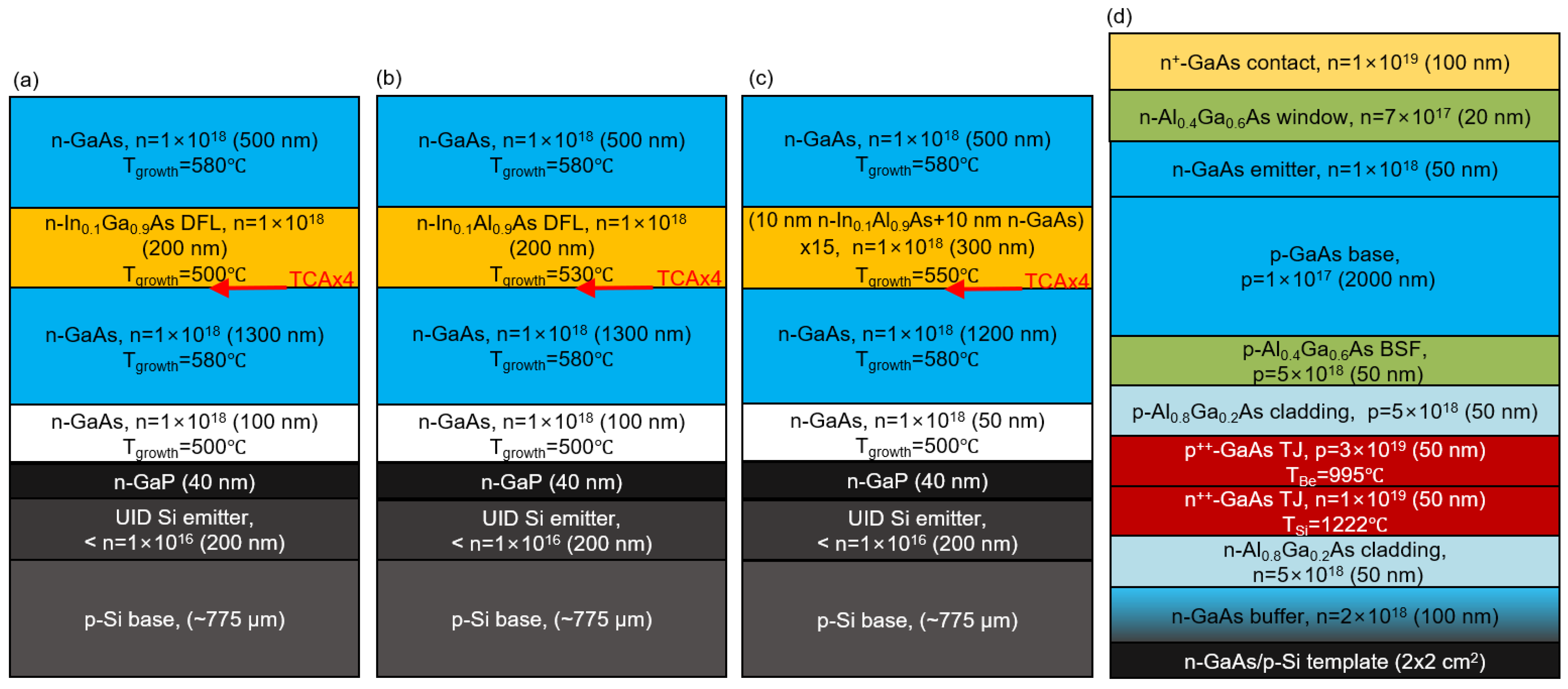
2. Epitaxial Growth
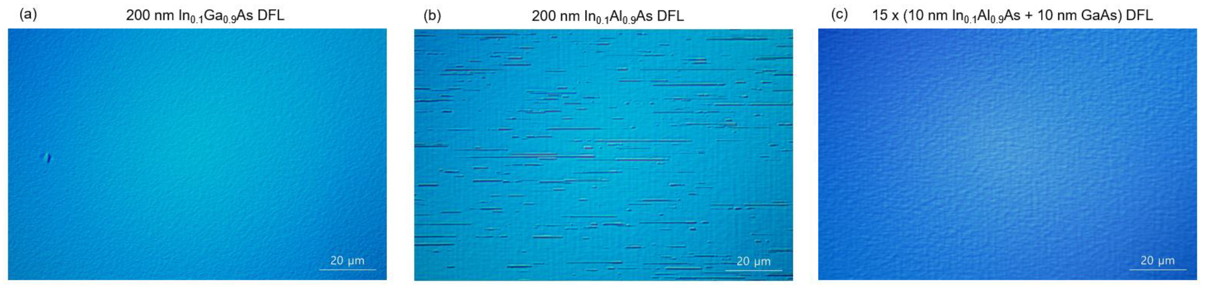
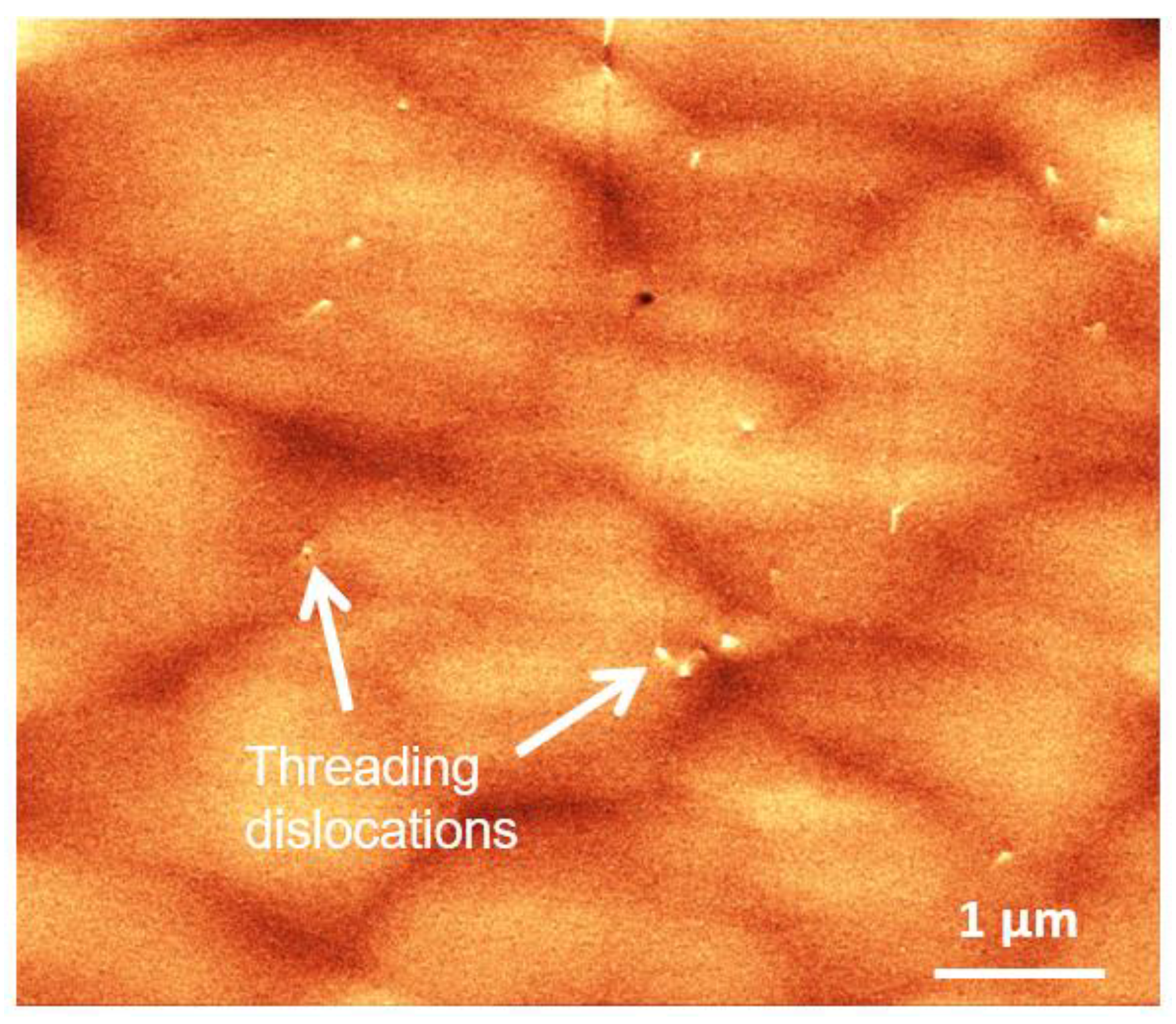
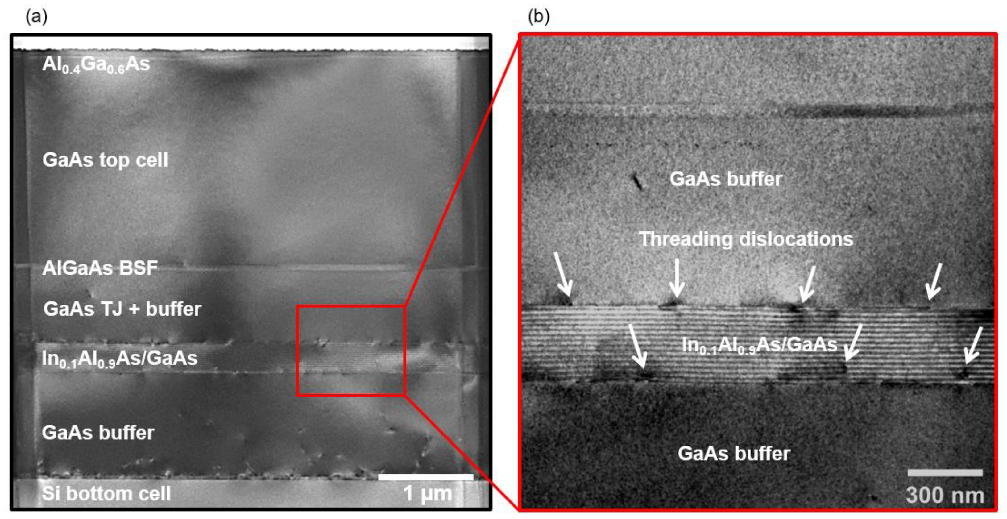
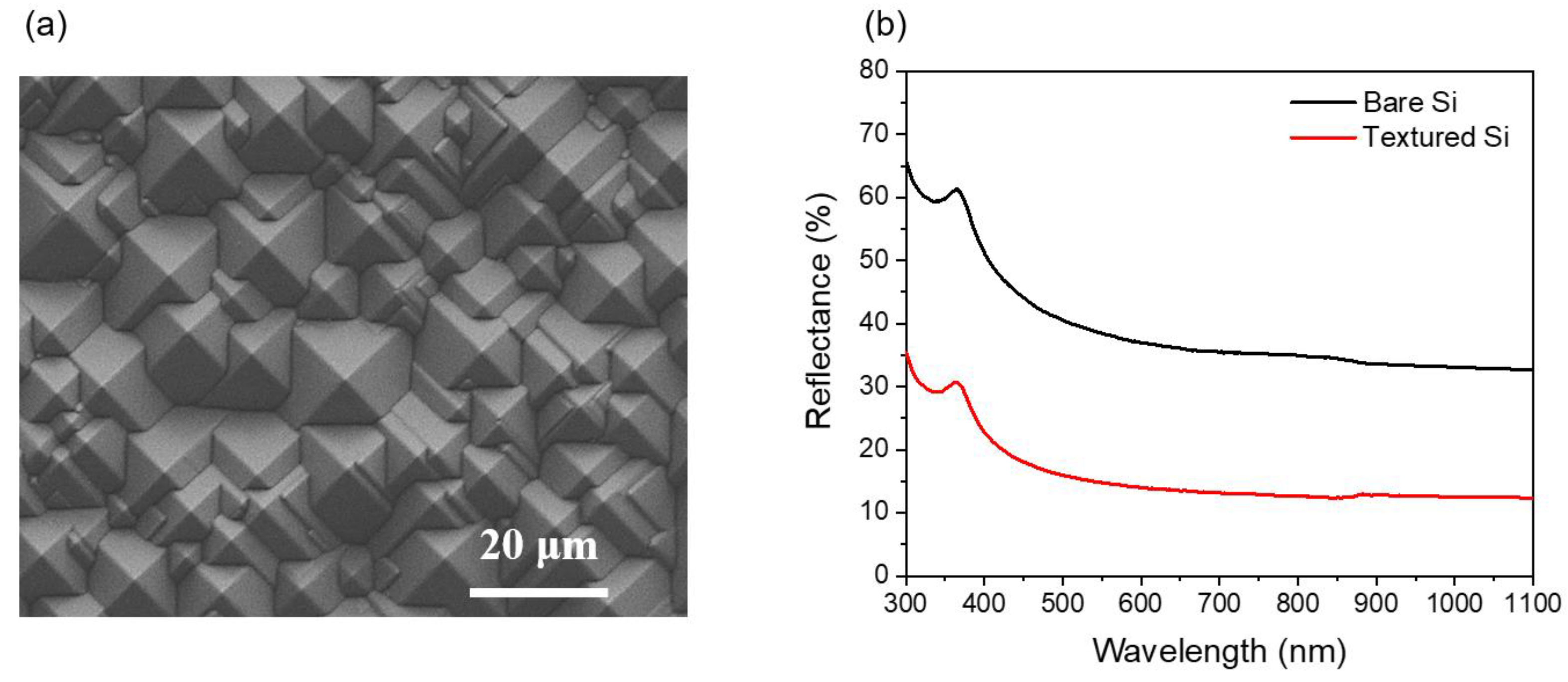
3. Material Characterizations
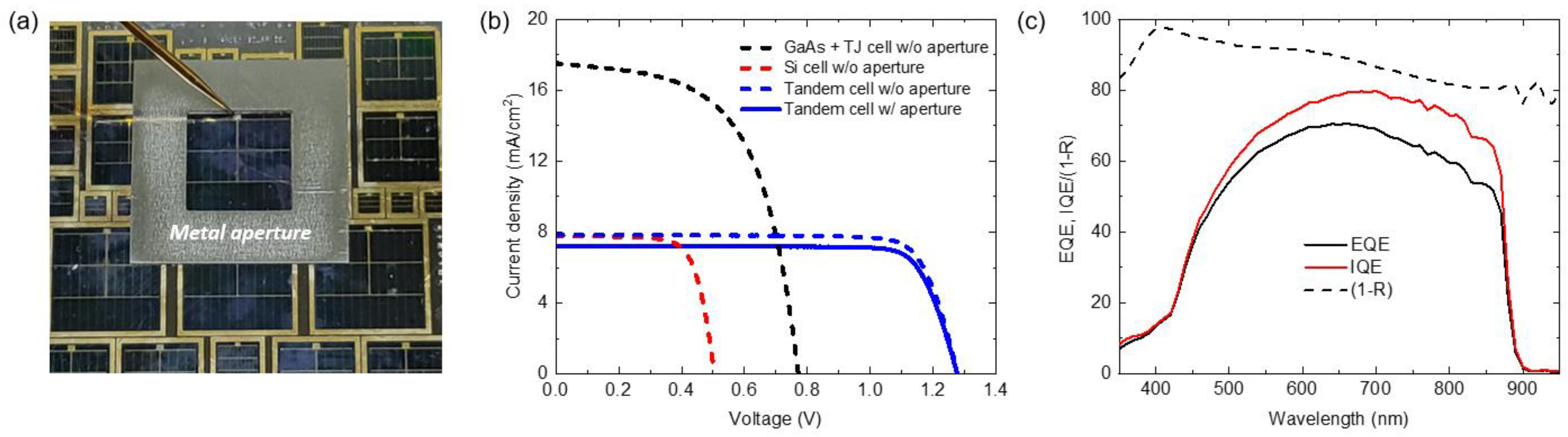
4. Cell Fabrication and Measurement
5. Conclusions
Author Contributions
Funding
Data Availability Statement
Conflicts of Interest
References
- Feifel, M.; Lackner, D.; Schon, J.; Ohlmann, J.; Benick, J.; Siefer, G.; Predan, F.; Hermle, M.; Dimroth, F. Epitaxial GaInP/GaAs/Si Triple-Junction Solar Cell with 25.9% AM1.5g Efficiency Enabled by Transparent Metamorphic AlxGa1-xAsyP1-y Step-Graded Buffer Structures. Sol. Rrl. 2021, 5, 2000763. [Google Scholar] [CrossRef]
- Green, M.A.; Dunlop, E.D.; Hohl-Ebinger, J.; Yoshita, M.; Kopidakis, N.; Bothe, K.; Hinken, D.; Rauer, M.; Hao, X.J. Solar cell efficiency tables (Version 60). Prog. Photovolt. 2022, 30, 687–701. [Google Scholar] [CrossRef]
- Essig, S.; Allebe, C.; Remo, T.; Geisz, J.F.; Steiner, M.A.; Horowitz, K.; Barraud, L.; Ward, J.S.; Schnabel, M.; Descoeudres, A.; et al. Raising the one-sun conversion efficiency of III-V/Si solar cells to 32.8% for two junctions and 35.9% for three junctions. Nat. Energy 2017, 2, 1–9. [Google Scholar] [CrossRef]
- Cano, P.; Hinojosa, M.; Garcia, I.; Beanland, R.; Marron, D.F.; Ruiz, C.M.; Johnson, A.; Rey-Stolle, I. GaAsP/SiGe tandem solar cells on porous Si substrates. Sol. Energy 2021, 230, 925–934. [Google Scholar] [CrossRef]
- Fan, S.Z.; Yu, Z.J.; Hool, R.D.; Dhingra, P.; Weigand, W.; Kim, M.J.; Ratta, E.D.; Li, B.D.; Sun, Y.K.; Holman, Z.C.; et al. Current-Matched III-V/Si Epitaxial Tandem Solar Cells with 25.0% Efficiency. Cell Rep. Phys. Sci. 2020, 1, 100208. [Google Scholar] [CrossRef]
- Feifel, M.; Lackner, D.; Ohlmann, J.; Benick, J.; Hermle, M.; Dimroth, F. Direct Growth of a GaInP/GaAs/Si Triple-Junction Solar Cell with 22.3% AM1.5g Efficiency. Sol. Rrl. 2019, 3, 1900313. [Google Scholar] [CrossRef] [Green Version]
- Soga, T.; Kato, T.; Yang, M.; Umeno, M.; Jimbo, T. High-Efficiency Algaas/Si Monolithic Tandem Solar-Cell Grown by Metalorganic Chemical-Vapor-Deposition. J. Appl. Phys. 1995, 78, 4196–4199. [Google Scholar] [CrossRef]
- Lepkowski, D.L.; Grassman, T.J.; Boyer, J.T.; Chmielewski, D.J.; Yi, C.Q.; Juhl, M.K.; Soeriyadi, A.H.; Western, N.; Mehrvarz, H.; Romer, U.; et al. 23.4% monolithic epitaxial GaAsP/Si tandem solar cells and quantification of losses from threading dislocations. Sol. Energ Mat. Sol. C 2021, 230, 111299. [Google Scholar] [CrossRef]
- Feifel, M.; Ohlmann, J.; Benick, J.; Hermle, M.; Belz, J.; Beyer, A.; Volz, K.; Hannappel, T.; Bett, A.W.; Lackner, D.; et al. Direct Growth of III-V/Silicon Triple-Junction Solar Cells With 19.7% Efficiency. IEEE J. Photovolt. 2018, 8, 1590–1595. [Google Scholar] [CrossRef]
- Kim, Y.; Chu, R.J.; Ryu, G.; Woo, S.; Lung, Q.N.D.; Ahn, D.H.; Han, J.H.; Choi, W.J.; Jung, D.H. Enhanced Photoluminescence of 1.3?m InAs Quantum Dots Grown on Ultrathin GaAs Buffer/Si Templates by Suppressing Interfacial Defect Emission. ACS Appl. Mater. Inter. 2022, 14, 45051–45058. [Google Scholar] [CrossRef]
- Hong, N.; Chu, R.J.; Kang, S.S.; Ryu, G.; Han, J.H.; Yu, K.J.; Jung, D.; Choi, W.J. Flexible GaAs photodetector arrays hetero-epitaxially grown on GaP/Si for a low-cost III-V wearable photonics platform. Opt. Express 2020, 28, 36559–36567. [Google Scholar] [CrossRef] [PubMed]
- Jung, D.H.; Zhang, Z.Y.; Norman, J.; Herrick, R.; Kennedy, M.J.; Patel, P.; Turnlund, K.; Jan, C.; Wan, Y.T.; Gossard, A.C.; et al. Highly Reliable Low-Threshold InAs Quantum Dot Lasers on On-Axis (001) Si with 87% Injection Efficiency. ACS Photonics 2018, 5, 1094–1100. [Google Scholar] [CrossRef]
- Jung, D.; Norman, J.; Kennedy, M.J.; Shang, C.; Shin, B.; Wan, Y.T.; Gossard, A.C.; Bowers, J.E. High efficiency low threshold current 1.3 mu m InAs quantum dot lasers on on-axis (001) GaP/Si. Appl. Phys. Lett. 2017, 111, 122107. [Google Scholar] [CrossRef]
- Jung, D.; Callahan, P.G.; Shin, B.; Mukherjee, K.; Gossard, A.C.; Bowers, J.E. Low threading dislocation density GaAs growth on on-axis GaP/Si (001). J. Appl. Phys. 2017, 122, 225703. [Google Scholar] [CrossRef] [Green Version]
- Ryu, G.; Woo, S.; Kang, S.S.; Chu, R.J.; Han, J.H.; Lee, I.H.; Jung, D.; Choi, W.J. Optimized InAlAs graded buffer and tensile-strained dislocation filter layer for high quality InAs photodetector grown on Si. Appl. Phys. Lett. 2020, 117, 262106. [Google Scholar] [CrossRef]
- Hool, R.D.; Sun, Y.K.; Li, B.D.; Dhingra, P.; Tham, R.W.; Fan, S.Z.; Lee, M.L. Challenges of relaxed n-type GaP on Si and strategies to enable low threading dislocation density. J. Appl. Phys. 2021, 130, 243104. [Google Scholar] [CrossRef]
- Amano, C.; Sugiura, H.; Yamamoto, A.; Yamaguchi, M. 20.2-Percent Efficiency Al0.4ga0.6as Gaas Tandem Solar-Cells Grown by Molecular-Beam Epitaxy. Appl. Phys. Lett. 1987, 51, 1998–2000. [Google Scholar] [CrossRef]
- Cho, H.K.; Lee, J.Y.; Kwon, M.S.; Lee, B.; Baek, J.H.; Han, W.S. Observation of phase separation and ordering in the InAlAs epilayer grown on InP at the low temperature. Mat. Sci. Eng. B-Solid 1999, 64, 174–179. [Google Scholar] [CrossRef]
- Yaung, K.N.; Kirnstoetter, S.; Faucher, J.; Gerger, A.; Lochtefeld, A.; Barnett, A.; Lee, M.L. Threading dislocation density characterization in III-V photovoltaic materials by electron channeling contrast imaging. J. Cryst. Growth 2016, 453, 65–70. [Google Scholar] [CrossRef] [Green Version]
- Fan, S.Z.; Jung, D.W.; Sun, Y.K.; Li, B.D.; Martin-Martin, D.; Lee, M.L. 16.8%-Efficient n(+)/p GaAs Solar Cells on Si With High Short-Circuit Current Density. IEEE J. Photovolt. 2019, 9, 660–665. [Google Scholar] [CrossRef]
- Wang, J.Q.; Zhong, F.Q.; Liu, H.; Zhao, L.; Wang, W.J.; Xu, X.X.; Zhang, Y.Z.; Yan, H. Influence of the textured pyramid size on the performance of silicon heterojunction solar cell. Sol. Energy 2021, 221, 114–119. [Google Scholar] [CrossRef]
- Ma, R.; Yan, C.; Fong, P.W.K.; Yu, J.; Liu, H.; Yin, J.; Huang, J.; Lu, X.; Li, G. In situ and ex situ investigations on ternary strategy and co-solvent effects towards high-efficiency organic solar cells. Energy Environ. Sci. 2022, 15, 2479–2488. [Google Scholar] [CrossRef]
- Ma, R.; Yan, C.; Yu, J.; Liu, T.; Liu, H.; Li, Y.; Chen, J.; Luo, Z.; Tang, B.; Lu, X.; et al. High-efficiency ternary or ganic solar cells with a good figure-of-merit enabled by two low-cost donor polymers. ACS Energy Lett. 2022, 7, 2547–2556. [Google Scholar] [CrossRef]


| Cells (5 mm × 5 mm) | Voc (V) | Jsc (mA/cm2) | FF (%) | Eff. (%) |
|---|---|---|---|---|
| GaAs cell w/o aperture | 0.78 | 17.4 | 58.7 | 7.8 |
| Si cell w/o aperture | 0.50 | 7.76 | 72.7 | 2.8 |
| Tandem cell w/o aperture | 1.28 | 7.84 | 80.8 | 8.0 |
| Tandem cell w/aperture | 1.28 | 7.19 | 81.7 | 7.5 |
Disclaimer/Publisher’s Note: The statements, opinions and data contained in all publications are solely those of the individual author(s) and contributor(s) and not of MDPI and/or the editor(s). MDPI and/or the editor(s) disclaim responsibility for any injury to people or property resulting from any ideas, methods, instructions or products referred to in the content. |
© 2023 by the authors. Licensee MDPI, Basel, Switzerland. This article is an open access article distributed under the terms and conditions of the Creative Commons Attribution (CC BY) license (https://creativecommons.org/licenses/by/4.0/).
Share and Cite
Kim, Y.; Madarang, M.A.; Ju, E.; Laryn, T.; Chu, R.J.; Kim, T.S.; Ahn, D.-H.; Kim, T.; Lee, I.-H.; Choi, W.J.; et al. GaAs/Si Tandem Solar Cells with an Optically Transparent InAlAs/GaAs Strained Layer Superlattices Dislocation Filter Layer. Energies 2023, 16, 1158. https://doi.org/10.3390/en16031158
Kim Y, Madarang MA, Ju E, Laryn T, Chu RJ, Kim TS, Ahn D-H, Kim T, Lee I-H, Choi WJ, et al. GaAs/Si Tandem Solar Cells with an Optically Transparent InAlAs/GaAs Strained Layer Superlattices Dislocation Filter Layer. Energies. 2023; 16(3):1158. https://doi.org/10.3390/en16031158
Chicago/Turabian StyleKim, Yeonhwa, May Angelu Madarang, Eunkyo Ju, Tsimafei Laryn, Rafael Jumar Chu, Tae Soo Kim, Dae-Hwan Ahn, Taehee Kim, In-Hwan Lee, Won Jun Choi, and et al. 2023. "GaAs/Si Tandem Solar Cells with an Optically Transparent InAlAs/GaAs Strained Layer Superlattices Dislocation Filter Layer" Energies 16, no. 3: 1158. https://doi.org/10.3390/en16031158