
Indirect Thermographic Temperature Measurement of a Power-Rectifying Diode Die Based on a Heat Sink Thermogram

1
Institute of Electric Power Engineering, Poznan University of Technology, Piotrowo 3A, 60-965 Poznan, Poland
2
Institute of Electrical Engineering and Electronics, Poznan University of Technology, Piotrowo 3A, 60-965 Poznan, Poland
*
Author to whom correspondence should be addressed.
Energies 2023, 16(1), 332; https://doi.org/10.3390/en16010332
Submission received: 9 November 2022
/
Revised: 21 December 2022
/
Accepted: 23 December 2022
/
Published: 28 December 2022
Abstract
:This article concerns the indirect thermographic measurement of the junction temperature of a D00-250-10 semiconductor diode. Herein, we show how the temperature of the semiconductor junction was estimated on the basis of the heat sink temperature. We discuss the methodology of selecting the points for thermographic measurement of the heat sink temperature and the diode case. The method of thermographic measurement of the heat sink temperature and the used measurement system are described. The simulation method used to obtain the temperature of the semiconductor diode junction on the basis of the thermographic measurement of the heat sink temperature, as well as the method of determining the emissivity and convection coefficients, is presented. In order to facilitate the understanding of the discussed issues, the construction of the diode and heat sink used, the heat flow equation and the finite element method are described. As a result of the work carried out, the point where the diode casing temperature is closest to the junction temperature was indicated, as well as which fragments of the heat sink should be observed in order to correctly estimate the temperature of the semiconductor junction. The indirect measurement of the semiconductor junction temperature was carried out for different values of the power dissipated in the junction.
1. Introduction
Devices adapted to supply alternating voltage consist of linear and non-linear elements [1]. The mentioned division is related to the shape of the current–voltage characteristic of the element. The use of an element with linear characteristics in the system does not pose many problems. Determining the working point of such an element is simple [2]. Additionally, the dependence of the values of selected quantities of linear elements on temperature (e.g., resistance of the resistors on the temperature of the resistor) has been described in the literature [3,4].
In the case of non-linear elements, working point determination is more difficult. As a result of the non-linear shape of the current–voltage characteristic, in order to determine the value of points outside the measuring points, interpolation should be performed using higher-order functions [5]. Determining the points on the characteristic described by means of a higher-order function is difficult and requires more skills [6].
The temperature of a non-linear element affects the shape of its current–voltage characteristic [7]. This means that for the same element, the current–voltage characteristic determined at room temperature differs from the current–voltage characteristic determined at a sample temperature of 100 °C.
An example of a non-linear element is a semiconductor diode. It comprises one semiconductor junction between the p (positive) region and the n (negative) region [8]. The current–voltage characteristic of a semiconductor diode depends on the chemical composition of the crystal from which the semiconductor junction regions are made. Each semiconductor junction has an individual current–voltage characteristic for a given temperature due to the impossibility of producing two identical semiconductor crystals. The current–voltage characteristic of a semiconductor diode is also dependent on the temperature [3,8].
The temperature of a semiconductor diode depends on two factors: the ambient temperature and the value of the current that flows through the IF diode. When the value of the IF current is higher than the maximum acceptable IFAV value (in the case of the instantaneous value from the peak surge forward current IFSM), the temperature of the semiconductor junction is higher than the maximum acceptable temperature (Tjmax). As a consequence, the semiconductor junction is damaged [9]. The diode temperature also depends on the rectified AC current frequency, as well as the reverse recovery time.
The temperature of the semiconductor junction can be lowered using heat sink systems. The most often used systems are heat sinks, which are metal components attached to the case of the semiconductor diode. The amount of heat received by the heat sink depends on the surface of the heat sink, the type of material it is made of and the method of heat exchange between the heat sink and its surroundings [10,11,12].
One method of heat transfer is convection. Depending on the speed at which the air flows around the heat sink, convection can be divided into free convection, also called natural convection, and the forced convection [13]. Forced convection occurs when the movement of the air flowing around the heat sink is forced by an external factor, e.g., due to the operation of a fan. Heat removal from the heat sink also takes place by means of infrared (IR) radiation. The amount of heat given off by the heat sink through convection and IR radiation depends on the temperature of the heat sink (Th) [10,13].
The metal used to produce heat sinks is aluminum. In order to improve heat dissipation by radiation, the surface of the heat sink is anodized and blackened. The heat dissipation of the heat sink can be improved by increasing the surface of the heat sink. Increasing the surface area of the heat sink causes an increase in the amount of metal needed to manufacture it. As a consequence, the price of the heat sink increases [14]. The second reason for the increase in the price of heat sinks is the increase in the price of metals [15]. As a result of an increase in the price of heat sinks, the final price of the product containing the diodes and heat sinks increases.
The increase in the price of the heat sinks means that there is a need for a precise selection of a radiator for the diode used in each application. A heat sink is selected correctly when, given the assumed operating conditions of the device, it prevents overheating of the semiconductor diode junction [11,12]. For this reason, in order to evaluate the selection of a heat sink, the temperature of the junction of the semiconductor diode (Tj) should be determined.
The value of Tj can be determined by the indirect method, as well as by the direct method. The direct method consists of the direct application of a temperature sensor to the semiconductor junction or the thermographic measurement of the temperature of the semiconductor junction placed in the opened case. The use of this method (the direct method) involves damaging the case [16]. The operating conditions of a semiconductor junction located in an opened case differ from the operating conditions of a semiconductor junction located in a closed case and from real conditions. For this reason, the result achieved with these methods has no practical significance.
The indirect method consists of determining the Tj of the semiconductor diode junction on the basis of the temperature of the case (TC) or on the basis of the measured value of the thermal sensitive parameter (TSP) [17]. Determining the value of Tj on the basis of the known value of the selected TSP is possible only if the dependence of TSP on Tj for a given DUT (device under test) is known. In the discussed case, the term DUT should be understood as the junction of a semiconductor diode. The dependence of the selected TSP on Tj is characteristic of a given DUT. To determine this dependence, the DUT must be placed in a specially prepared measuring system. The use of this method is time-consuming and suitable for the laboratory applications [18].
The value of Tj can be determined on the basis of the known values of the temperature of the case (TC), the thermal resistance of the junction case (ϑjc) and the power dissipated in the semiconductor diode junction (Pj). The dependence is described in JESD 51-12-01. The TC value can be measured by a sensor placed on the case. It is dangerous to carry out such a measurement, as there is a risk of electric shock. Applying a sensor to the case disturbs the temperature distribution on its surface. The value of the thermal resistance between the diode case and the sensor case is also unknown and difficult to determine. Another problem is the cost of the sensor and the special glue [19].
These problems can be avoided by using thermographic measurement. The use of this non-contact method enables the measurement of the temperature on the surface of the diode case. Thermographic measurement is faster than gluing a temperature sensor to the case, which is difficult. The result of thermographic measurement of the diode temperature depends on a number of factors, the most important of which include the value of the emissivity coefficient (ε) [20], the reflected temperature (Tr) [21], the distance between the lens and the observed object (d) [22], the ambient temperature (Ta) [23], the temperature of the external optical system [24], the transmittance of the external optical system [25,26], the relative humidity (ω) [27], the viewing angle (β) [28] and the sharpness of the recorded thermogram [29,30,31].
The dependence between Tj, TC and ϑjc described in JESD 51-12-01 does not allow for estimation of the dependence between Tj and Th. The methods described in the literature that allow for the estimation of the Tj and Th are the Cauer [32] and Foster [33] methods for modeling the heat flow path on the junction–heat sink route. Fourier transform has also been used to simplify the equations [34]. One-dimensional [35] and three-dimensional [36] temperature distribution models have also been proposed. There is also a known method of thermal impedance reconstruction in a heat source based on the measurement of IR radiation on the surface of an electronic device [37].
The proposed methods require advanced knowledge of mathematics. A further disadvantage of these methods is the possibility of obtaining temperature distribution along the selected path (1D solution). It may be not enough for a quick assessment of the correct-ness of the heat sink selection, and another method is needed. In practice, the diode case temperature is known. This temperature can be measured with a thermographic camera. Thermographic measurement obtains a map of temperatures on the diode case. The power dissipated on a diode junction can also be measured. For a quick assessment of the correctness of the heat sink selection, it is necessary to know the difference between Tj and Th. This difference can be obtained using the temperature distribution on the diode case and the diode case thermographic temperature measurement (as a boundary condition).
The discussed temperature distributions can be obtained on the basis of numerical methods. One such method is the FEA (finite element analysis) method. By definition, FEA is a numerical method for solving problems in engineering and mathematical physics [38]. The performance of the correct temperature distributions requires knowledge of the properties of the materials from which the diode and the heat sink are made. Additionally, it requires knowledge of the Prandtl, Nusselt and Grashof numbers. If the forced convection is taken into account, it is also necessary to calculate the Rayleigh number. The equations enabling the determination of these numbers have been described in the literature [33].
FEA can be used to determine the temperature distribution over a wide range of diodes, IGBTs and MOSFET transistors. In some cases, the die is placed in a mold body made of epoxy resin. Removing the mold body breaks the bond wires connecting to the leads. Consequently, the thermographic temperature measurement of die is not possible. Electrical methods of determining the temperature of a die do not allow for attainment of the temperature distribution on its surface. For this reason, verification of the temperature distribution obtained as a result of simulation work is difficult.
To the best of our knowledge, this is the first study dealing with the problem of the verification of the selection of heat sinks for power diodes based on the thermographic measurement of the temperature case and the temperature distribution determined by numerical methods. An additional problem that makes thermographic measurement of the diode case temperature difficult is the cylindrical shape of the diode case, which is made of metal, a material with a low ε value. For this reason, it was decided to undertake this research work, the consequence of which will be to fill this gap. It was also decided to verify the usefulness of FEA by verifying the obtained temperature distribution. For this purpose, a D00-250-10 diode was used, which is characterized by easy access to the die.
2. Materials and Methods
2.1. Thermographic Measurement of the Temperature of the Diode Case and the Heat Sink Surface
The verification of the correctness of the selection of a heat sink for a semiconductor diode requires knowledge of the dependence between Th and Tj. On the other hand, determination of the Tj value on the basis of the Ta value measured with a thermographic camera (the indirect method) requires the correct thermographic measurement and knowledge of the dependence between Tj and Ta [39].
In the conducted research, it was decided to use a D00-250-10 power diode (Lamina, Piaseczno, Poland) (IF = 250 A, UF = 1.5 V), which is used in the construction of the welding machines. The diode is placed on a heat sink made of aluminum. The dimensions of the heat sink are shown in the Figure 1.
Performing the correct thermographic measurement of the diode surface requires knowledge of the values of the emissivity coefficients. The ε value depends, among other factors, on the material from which the diode and heat sink surface are made, as well as the temperature and the condition of the surface. The value of ε can be read from the available tables in the literature and determined experimentally, as in [17].
The elements used in this were the elements that were placed in a working device. For this reason, their surface was scratched and covered with metal oxides. It was decided to use paint with a known ε value. Marks were made in places where the thermographic temperature of the case was measured. Velvet Coating 811-21 paint with a specific emissivity coefficient value ranging from 0.970 to 0.975 for temperatures from −36 °C to 82 °C was used. The locations of the markers on the diode case and the heat sink surface are shown in Figure 2.
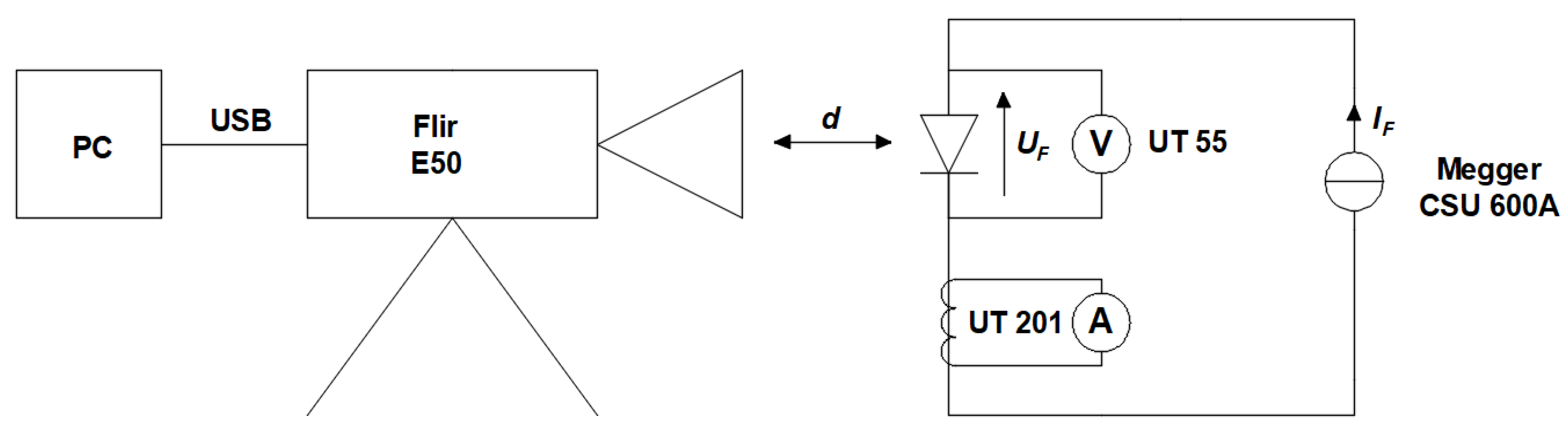
The diode prepared in this way and placed on the heat sink (Figure 1 and Figure 2) was placed in the measuring system. The value of the IF flowing through the DUT (in this study, a semiconductor diode junction) was forced by a CSU 600 A power source (Megger, Dover, England). The UF value at the DUT inputs was measured with a UT51 multimeter (UNI-T, Dongguan, China), whereas the IF value was measured with a UT55 (UNI-T, Dongguan, China). Thermographic measurement of the diode and heat sink surface temperatures was performed with a Flir E50 thermal camera (Flir, Wilsonville, OR, USA). The absolute value errors of the forward current of the diode ΔIF were determined using Equation (1) [40]:
The value of the measurement error of the forward voltage was determined by Equation (2) [41]:
The measurement error (ΔTa) made with a thermographic camera was 2 °C or 2% of the measured value. The greater value was taken as the value of ΔTa.
Due to the shape of the semiconductor diode case, which resembled a cylinder, the observed marker (placed on the diode case) had to be placed perpendicular to the camera lens. Incorrect placement of the marker on the diode case could result in an increase in the error value related to the phenomenon of the angular emissivity [42]. The place where the Tc value was measured was selected on the basis of the works presented in [17]. A diagram of the measuring system is shown in Figure 3.
2.2. Determining the Dependence between the Case Temperature and the Junction Temperature by Simulating the Temperature Distribution
Determination of the temperature distribution in the area between the case and the semiconductor diode junction and between the semiconductor diode junction and the radiator is possible when numerical methods are used. One such method is the finite element method (FEA), which consists of dividing the analyzed object into a specific number of finite elements and nodes located at the vertices of the finite elements. Then, on the basis of defined boundary conditions and the shape functions (the functions interpolating the values inside the finite elements based on the values in the nodes), the searched values in a given area are determined [43].
The software applied in this study was Solidworks 2020 SP05 (Dassault Systèmes, Vélizy-Villacoublay, France), which uses FEA. The software divides the created model into tetrahedral finite elements. Their number can be specified by the user. The more complex the model is, the more finite elements and nodes. On the other hand, the more the number of nodes increases, the more time needed to calculate the values in these nodes and obtain the desired temperature distribution.
The heat conduction equation for a transient state in a three-dimensional element can be described by a second-order differential Equation (3) [44]:
where c is the specific heat; is the density (kg/m3); Q(x,y,z,t) (J) is the rate of the internal heat generation; kx, ky and kz (W/m·K) are the thermal conductivities in the x, y and z directions, respectively; T (K) is the temperature; and t (s) is the time.
According to the finite element method, the area where the temperature distribution is searched is divided into the tetrahedral elements. In each of the tetrahedral elements, the temperature field is interpolated based on the temperature in the nodes of this element, and the linear shape functions are determined according to Equation (4) [44]:
where Ti(t) is the nodal temperature at node i, and Hi is the linear shape function.
In the Cartesian system, the linear function from Equation (4) for node i (the tetrahedral element) can be expressed by Equation (5) [45]:
where i = 1,…,4, ai, bi, i and di are the coefficients.
As a result, a system of equations for the unknown coefficients can be obtained. This procedure must then be repeated for all mesh nodes. In order to obtain a discrete system of equations, the functions of the shape should be derived and integrated. When the edge of the tetrahedral element does not match the coordinate system, the computation becomes more complicated. In this case, each point (x, y and z) of the original coordinate system can be transformed to another point (ξ, η and ζ) in the transformed coordinate system by Equation (6) [46]:
It is possible to arrange the Jacobi matrix (J) according to Equation (7):
Consequently, the shape functions for the transformed coordinate system can be written using Equation (8) [46]:
In the steady state, when the heat flow in one direction in a homogeneous environment is considered, when there is no internal heat generation, Equation (3) can be simplified to Equation (9) [17]:
where φ is a radiative heat flux (W∙m−2).
After separating the variables and integrating Equation (9) on both sides, the time constant can be obtained from the following boundary conditions (Equation (10)):
where xk is the end point of the analyzed heat flow path (m), T1 is the temperature at the starting point of the analyzed heat flow path (K) and T2 is the temperature at the end point of the analyzed heat flow path (K).
After determining the time constant, when φ penetrates the entire wall, Equation (9) takes the form of Equation (11) [47]:
where Pc is the total power applied to the wall (W), and S (m2) is the area of the wall penetrated by φ (W∙m−2).
Analysis of Equation (11) shows that in order to determine the desired temperature distribution, it is necessary to determine the geometry of the model and the power released in the semiconductor element. The geometric model can be determined by creating a software model. Furthermore, in order to determine the desired temperature distributions, it is necessary to know the power released at the semiconductor junction (Pj). The Pj value was obtained from the measured UF and IF values according to Equation (12):
It was assumed that all Pj allocated at the junction was converted into an increase in the temperature of the junction. In Equation (3), the cosφ value was not taken into account due to the high value close to 1. The error value (ΔPj) is determined using Equation (13) [48]:
The high cosφ value was experimentally verified on the basis of the measured values of inductance (L), capacitance (C) and resistance (R). The R, C and L values of the diode were measured using an LCR HM 8118 bridge (Hameg, Mainhausen, Germany). Based on the measured values of L and C, the reactance (X) of the diode was determined. The value of φ was obtained as the arctangent of the quotient of X and R.
Determination of the temperature distribution also requires determination of the convection coefficient (hc) value. The hc coefficient was selected using the theory of similarity to the physical phenomena. The relationships with the physical quantities characterizing a given phenomenon were described using the criteria of Nusselt, Grashof and Prandtl.
The value of hcr for a cylindrical surface can be determined according to Equation (14) [32]:
where hcr is the convection coefficient of the cylindrical surface (W∙m−2∙K−1), g is the gravitational acceleration of 9.8 (m∙s−2), dr is equal to the work roll diameter (a characteristic size in this case) (m), Pr is the Prandtl number (–), α is a coefficient of expansion equal to 0.0034 (K−1) and ν is kinematic viscosity equal to 1.9 × 10⁻⁵ (m2∙s−1).
The Prandtl number can be obtained from Equation (15) [17]:
where c is the specific heat of air equal to 1005 (J∙kg−1∙K−1) in 293.15 (K), and η is dynamic air viscosity equal to 1.75 × 10⁻⁵ (kg∙m−1∙s−1) in 273.15 (K).
In the case of determining the convection coefficient for a flat surface, Equation (16) [17] should be used instead Equation (14):
where hcf is the convection coefficient of flat surfaces, Nu is the Nusselt number (-) and L is the characteristic length in meters (for a vertical wall, this value represents height).
In order to calculate the Nusselt number, the Prandtl number and the Grashof number (Gr) must be known. The Prandtl number can be obtained using Equation (15). The Grashof number can be determined using Equation (17) [17]:
The Nusselt number is described by Equation (18) [17]:
where a and b are dimensionless coefficients, the values of which depend on the shape and the orientation of the analyzed surface and the product of Pr·Gr. The values of coefficients a and b are presented in Table 1. Then, by inserting the result of Equation (18) into Equation (16), the value of hcf can be determined.
Determination of the searched temperature distributions requires the determination of the radiation coefficient (hr). The hr coefficient defines the amount of thermal energy transferred to the environment by radiation per unit time, per unit area and per unit temperature difference between the body radiating energy and the environment. In the software used in the present study, the hr value is determined on the basis of all entered data and does not need to be entered. When the software requires the introduction of the hr value, this value can be determined on the basis of Equation (19) [17]:
where σc is the Stefan–Boltzmann constant equal to 5.67 × 10⁻⁸ (W∙m−2∙K−4)), TS is the surface temperature (K) and Ta is the air temperature (K).
Analysis of Equations (3) and (11) shows that in order to determine the temperature distribution, it is necessary to know the value of the specific thermal conductivity coefficient (k). As the metal alloys from which the diode case was made were not exactly known, the values of coefficient k were determined by simulation. Knowing the temperature values on the diode surfaces, the power dissipated at the junction and the values of convection and radiation coefficients, the k values were selected so that the simulation results were consistent with the results of the thermographic measurements of the temperature of the diode case and the heat sink (Figure 1 and Figure 2). On the basis of the selected values of the thermal conductivity coefficient (k), the material from which the given surface was used was identified.
3. Results
Performing the simulation work required the determination of the values of the ε coefficients and the hc convection. The hc coefficient values were determined for each of the points presented in Figure 2, in accordance with the rules presented in Section 2.2. The selected values of ε and hc for the different values of Pj are presented in the Table 2 and Table 3.
The captured thermograms are shown in Figure 4, Figure 5, Figure 6, Figure 7 and Figure 8. The applied markers can be observed on the thermograms.
Before starting the simulation work, the relationship between the mesh size, the simulation time (ts) and the obtained result was checked. The results are shown in Figure 9, Figure 10 and Figure 11.
The temperature results at the points shown in Figure 2 obtained from the Ts simulation were compared with the values obtained from the TC measurements presented in Table 4 and Table 5.
The results of the performed simulations are shown in Figure 12, Figure 13, Figure 14, Figure 15 and Figure 16.
4. Discussion
Information about the temperature of a semiconductor junction is important to designers. When the semiconductor junction is operated at the correct temperature, the current–voltage characteristics of the diode conform to the characteristics that have been taken into account by the designer. As the temperature of the semiconductor junction increases, the shape of the IF = f (UF) characteristic changes. As a consequence, the flow of currents in the device in which this connector is placed changes. An excessively high temperature of a semiconductor junction may shorten its life, causing malfunctions and damage.
The temperature of a semiconductor junction can be lowered by placing a diode on the heat sink. Due to incorrect selection of the heat sink, the semiconductor junction may not reach the assumed temperature. Another negative phenomenon is the oversizing of the heat sink, which is associated with unnecessary expense. The correctness of the heat sink selection can be assessed by measuring the temperature of the semiconductor junction. It is impossible to directly measure the temperature of the semiconductor junction without damaging the case of the semiconductor diode.
The solution to this problem is to perform an indirect measurement of the semiconductor junction temperature on the basis of the generated thermogram. As an auxiliary tool, the assessment of the junction temperature on the basis of mathematical simulations was proposed. The main objective of the present study was to check whether a reliable assessment of the temperature of the semiconductor junction can be made based on the thermographic measurement of the heat sink temperature.
In order to determine the appropriate measurement point on the heat sink, a simulation was carried out in the Solidworks program. The credibility of the performed simulation was confirmed by means of thermographic measurements. The performed simulation made it possible to select the optimal measurement point, i.e., the point where the smallest difference between the temperature of this point and the temperature of the semiconductor diode junction occurred. The simulation required knowledge of the ε and hc coefficients. Our proposed values of these coefficients were confirmed by comparing the simulation results for different powers of the junction with the results of thermographic measurements. Accordingly, we showed that it is possible to perform such a thermographic measurement of the heat sink temperature to determine the temperature of the semiconductor diode junction based on simulation results.
The simulation results were compared with the results obtained with the use of other methods. It was noted that the values of the appearing discrepancies did not exceed the measurement error of the instrument used. This led to the conclusion that a combination of thermographic temperature measurement and simulation could be useful for assessing the temperature of a semiconductor junction based on the temperature of the case. The analysis of thermographic measurements and the test results confirmed these conclusions. Furthermore, thermal differentiation in the analyzed points was confirmed. For this reason, incorrect or excessively general selection of the values of the ε and hc coefficients may be a source of additional errors. As predicted, according to the simulation results, the part of the heat sink indicated in this study was confirmed to be the best measurement area. This correctness was confirmed for different powers emitted at the semiconductor diode junction.
5. Conclusions
Placing a semiconductor diode on the heat sink lowers the temperature of its junction. This enables proper operation, during which the current–voltage characteristics of the semiconductor junction are consistent with the characteristics that were taken into account by the device designer during the design. It is also possible to protect the semiconductor diode junction from overheating, which can cause malfunctions, reduced service life and even damage to the semiconductor junction.
Oversizing of the heat sink causes the final cost of the product to increase. For this reason, it is necessary to select the heat sink to ensure the correct temperature of the semiconductor junction with the lowest financial outlay. Therefore, in the prototyping stage, it is important to monitor the junction temperature of the semiconductor diode placed on the radiator.
It is impossible to perform a direct measurement of the temperature of the semiconductor diode junction without opening the case. On the other hand, indirect measurement with a temperature sensor applied to the heat sink in combination with simulation can be dangerous. There is a risk of accidentally applying the temperature sensor to a conductive part, resulting in electric shock. This risk can be eliminated by using thermography.
The application of this non-contact method is difficult in cases in which the radiator is made of aluminum—a metal with a low emissivity factor value. This problem can be solved by using a blackened heat sink, which has a high emissivity. Paint with a known emissivity can also be used. The use of thermography facilitates the shape of the heat sink; it is easy to find a surface parallel to the lens of a thermographic camera, avoiding errors due to a change in angular emissivity.
When interpreting thermograms, it should be remembered that the surfaces of the element that on the thermogram may have different emissivity coefficient values. As a result of corrosion and mechanical damage, the local value of the emissivity factor may differ from the value of the emissivity factor of the rest of the element. Consequently, this fragment may have a visibly different temperature, as shown in the presented thermograms (Figure 4, Figure 5, Figure 6, Figure 7 and Figure 8), in which the temperature of a piece covered with paint with a known emissivity value appears to be different from the temperature of another part of the heat sink.
Analysis of the data from Table 4 and Table 5 show that for a power (Pj) of less than 50 W, the difference between the values obtained from simulations (TS) and the values of the case temperature (TC) is less than 2 °C. Moreover, the indications of the thermographic camera are smaller than the error. As the value of Pj increases, the differences between the TS and TC values increase. This is due to the choice of emissivity and convection coefficients. The local value of the emissivity coefficient could differ from the value of the emissivity coefficient selected for the surface. The values obtained as a result of the simulation are more influenced by the selection of the convection coefficient.
The temperature value obtained (as a result of the simulation) at the selected point depends on the size of the grid selected during the simulation. The mesh size affects the duration of the simulation. The smaller the grid, the more points in the grid. As the number of points increases, the simulation time increases. It is possible to find a grid size that allows for attainment of sufficiently accurate results (optimal size). Further reduction of the mesh does not make sense; the obtained simulation results do not improve, whereas the time needed to perform the simulation increases. For this reason, the optimal mesh size should be checked before starting work.
In this study, a method was used that allows for attainment the approximate values of the convection coefficients. In order to obtain accurate values of the convection coefficients, experimental work should be carried out. On the basis of the obtained results (Table 4 and Table 5), it can be concluded that FEM can be used to obtain a sufficiently accurate temperature distribution, provided that the values of emissivity coefficients and the convection coefficients are correctly selected.
Analysis of the data presented in Table 7 shows that the temperature recorded at point 4 (Figure 2) is the closest to the temperature of the semiconductor junction. This is the point on the part of the semiconductor diode case that is closest to the semiconductor junction. It is possible to find such a surface of this fragment which is parallel to the lens of the thermographic camera (no influence of the angular emissivity on the value of the thermographic temperature measurement). The only problem is the low value of the emissivity factor of this surface.
Analysis of the data presented in Table 7 also shows that in the case of the points located on the heat sink (points 5–22), the differences between the heat sink temperature and the temperature of the semiconductor junction (Tj − TS) are minimal. The difference between the largest and the smallest (Tj − TS) values for points 5–22 (Figure 2) is close to the error value of the thermographic camera used in this study. For this reason, it is possible to conclude that each of the selected points is suitable for estimation of the temperature of the semiconductor diode junction.
When performing a heat sink thermogram (for simulation work), it is not necessary to focus on a specific point. This is important because such thermographic temperature measurement of the heat sink is easier to perform. While performing thermographic temperature measurements of the heat sink, it is recommended to observe its upper part. It is also necessary to ensure the correct compensation of the reflected temperature and to perform the measurement in such a way that the measuring point is not in a place where the temperature from the adjacent element is reflected. This requires a skilled and experienced thermographer.
The presented results may be used in the course of other works that will be carried out in the future. One of the examples is the development of a system for continuous direct measurement of the semiconductor diode junction temperature. Such a system could be applied to an Internet of Things (IoT) node.
Author Contributions
Methodology, K.D. and A.H.; formal analysis, K.D. and A.H.; investigation, K.D., A.H. and Ł.D.; resources, K.D.; writing—original draft preparation, K.D., A.H., Ł.D. and G.D.; writing—review and editing, K.D., A.H., Ł.D. and G.D.; visualization, K.D.; supervision, K.D. and A.H. All authors have read and agreed to the published version of the manuscript.
Funding
This research was funded by the Ministry of Education and Science of Poland (grant numbers 0212/SBAD/0573 and 0711/SBAD/4560).
Data Availability Statement
Not applicable.
Conflicts of Interest
The authors declare no conflict of interest.
References
- Shanidze, L.V.; Tarasov, A.S.; Rautskiy, M.V.; Zelenov, F.V.; Konovalov, S.O.; Nemtsev, I.V.; Voloshin, A.S.; Tarasov, I.A.; Baron, F.A.; Volkov, N.V. Cu-Doped TiNxOy Thin Film Resistors DC/RF Performance and Reliability. Appl. Sci. 2021, 11, 7498. [Google Scholar] [CrossRef]
- Christodoulou, C.A.; Vita, V.; Mladenov, V.; Ekonomou, L. On the Computation of the Voltage Distribution along the Non-Linear Resistor of Gapless Metal Oxide Surge Arresters. Energies 2018, 11, 3046. [Google Scholar] [CrossRef] [Green Version]
- Jaritz, M.; Hillers, A.; Biela, J. General Analytical Model for the Thermal Resistance of Windings Made of Solid or Litz Wire. IEEE Trans. Power Electron. 2019, 3, 668–684. [Google Scholar] [CrossRef]
- Kim, D.; Nagao, S.; Chen, C.; Wakasugi, N.; Yamamoto, Y.; Suetake, A.; Takemasa, T.; Sugahara, T.; Saganuma, K. Online Thermal Resistance and Reliability Characteristic Monitoring of Power Modules With Ag Sinter Joining and Pb, Pb-Free Solders During Power Cycling Test by SiC TEG Chip. IEEE Trans. Power Electron. 2021, 36, 4977–4990. [Google Scholar] [CrossRef]
- Liu, C.; Sun, Q.; Dai, W.; Ren, Z.; Li, G.; Yu, F. A Method of Camera Calibration Based on Kriging Interpolation. IEEE Access 2021, 9, 153540–153547. [Google Scholar] [CrossRef]
- Jiang, Z.; Yan, C.; Yu, J. Efficient methods with higher order interpolation and MOOD strategy for compressible turbulence simulations. J. Comput. Phys. 2018, 371, 528–550. [Google Scholar] [CrossRef]
- Li, J.; Yang, S.; Pu, Y.; Zhu, D. Effects of pre-calcination and sintering temperature on the microstructure and electrical properties of ZnO-based varistor ceramic. Mater. Sci. Semicond. Process. 2021, 123, 105529. [Google Scholar] [CrossRef]
- Górecki, P.; Górecki, K. Pomiary i obliczenia temperatur wewnętrznych tranzystora IGBT i diody umieszczonej we wspólnej obudowie. Elektronika 2021, 10, 210. [Google Scholar]
- Megherbi, M.L.; Pezzimenti, F.; Dehimi, L.; Saadoune, M.A.; Della Corte, F.G. Analysis of Trapping Effects on the Forward Current–Voltage Characteristics of Al-Implanted 4H-SiC p-i-n Diodes. IEEE Trans. Electron. Devices 2018, 65, 3371–3378. [Google Scholar] [CrossRef]
- Lopes, A.M.G.; Costa, V.A.F. Improved Radial Plane Fins Heat Sink for Light-Emitting Diode Lamps Cooling. ASME J. Thermal Sci. Eng. Appl. 2020, 12, 041012. [Google Scholar] [CrossRef]
- Praveen, A.S.; Jithin, R.; Naveen-Kumar, K.; Baby, M. Analysis of thermal and optical characteristics of light-emitting diode on various heat sinks. Int. J. Ambient. Energy 2021, 42, 854–859. [Google Scholar] [CrossRef]
- Bechir Ben Hamida, M.; Almeshaal, M.A.; Hajlaoui, K.; Rothan, Y.A. A three-dimensional thermal management study for cooling a square Light Edding Diode. Case Stud. Therm. Eng. 2021, 27, 10122. [Google Scholar] [CrossRef]
- Safaei, M.R.; Karimipour, A.; Abdollahi, A.; Nguyen, T.K. The investigation of thermal radiation and free convection heat transfer mechanisms of nanofluid inside a shallow cavity by lattice Boltzmann method. Phys. A Stat. Mech. Appl. 2018, 509, 515–535. [Google Scholar] [CrossRef]
- Yahyaee, A.; Bahman, A.S.; Blaabjerg, F. Modyfikacja radiatora z przesuniętą listwą z wysokowydajnym chłodzeniem dla modułów IGBT. Zał. Nauka. 2020, 10, 1112. [Google Scholar]
- Gilbert, C.L. Warehouse load-out queues and aluminum prices. J. Commod. Mark. 2022, 28, 100243. [Google Scholar] [CrossRef]
- Kim, S.Y.; Jo, H.R.; Cho, S.; Lee, I.B. Estimation of Junction Temperature in a Two-Level Insulated-Gate Bipolar Transistor Inverter for Motor Drives. J. Electr. Eng. Technol. 2022, 17, 1111–1119. [Google Scholar] [CrossRef]
- Dziarski, K.; Hulewicz, A.; Dombek, G.; Drużyński, Ł. Indirect Thermographic Temperature Measurement of a Power-Rectifying Diode Die. Energies 2022, 15, 3203. [Google Scholar] [CrossRef]
- Yang, F.; Ugur, E.; Akin, B. Evaluation of Aging’s Effect on Temperature-Sensitive Electrical Parameters in SiC mosfets. IEEE Trans. Power Electron. 2020, 35, 6315–6331. [Google Scholar] [CrossRef]
- Lamuadni, B.; El Bouayadi, R.; Amine, A.; Zejli, D. Design and Development of a Measurement System Dedicated to Estimate the Junction Temperature of Insulated Gate Bipolar Transistor Modules. Int. J. Eng. Res. Afr. 2022, 60, 89–106. [Google Scholar] [CrossRef]
- Kałuża, M.; Więcek, B.; De Mey, G.; Hatzopoulos, A.; Chatziathanasiou, V. Thermal impedance measurement of integrated inductors on bulk silicon substrate. J. Microelectron. Reliab. 2017, 73, 54–59. [Google Scholar] [CrossRef]
- Więcek, B.; De Mey, G. Thermovision in Infrared–Basics and Applications; Measurement Automation Monitoring Publishing House: Warszawa, Poland, 2011. [Google Scholar]
- Minkina, W.; Dudzik, S. Infrared Thermography: Errors and Uncertainties; John Wiley & Sons: Hoboken, NJ, USA, 2009. [Google Scholar]
- Jung, G. A low-power embedded poly-Si micro-heater for gas sensor platform based on a FET transducer and its application for NO2 sensing. Sens. Actuators B Chem. 2021, 334, 129642. [Google Scholar] [CrossRef]
- Moure, A. In situ thermal runaway of Si-based press-fit diodes monitored by infrared thermography. Results Phys. 2020, 19, 103529. [Google Scholar] [CrossRef]
- Kandeal, A.W. Infrared thermography-based condition monitoring of solar photovoltaic systems: A mini review of recent advances. Sol. Energy 2021, 223, 33–43. [Google Scholar] [CrossRef]
- Aumeunier, M.H. Infrared thermography in metallic environments of WEST and ASDEX Upgrade. Nucl. Mater. Energy 2021, 26, 100879. [Google Scholar] [CrossRef]
- Dziarski, K.; Hulewicz, A.; Dombek, G.; Frąckowiak, R.; Wiczyński, G. Unsharpness of Thermograms in Thermography Diagnostics of Electronic Elements. Electronics 2020, 9, 897. [Google Scholar] [CrossRef]
- Van Erp, R.; Soleimanzadeh, R.; Nela, L. Co-designing electronics with microfluidics for more sustainable cooling. Nature 2020, 585, 211–216. [Google Scholar] [CrossRef]
- Nishi, K. Research on Package Thermal Resistance of Power Semiconductor Devices. In Proceedings of the 35th Semiconductor Thermal Measurement, Modeling and Management Symposium (SEMI-THERM), San Jose, CA, USA, 18–22 March 2019; pp. 61–65. [Google Scholar]
- Gao, J.; Wang, S.; Wang, J. Thermal Resistance Model of Packaging for RF High Power Devices. In Proceedings of the 2020 International Conference on Microwave and Millimeter Wave Technology (ICMMT), Shanghai, China, 20–23 September 2020; pp. 1–3. [Google Scholar]
- Kawor, E.T.; Mattei, S. Emissivity measurements for nexel velvet coating 811-21 between −36 °C and 82 °C, 15 ECTP Proceedings. High Temp. High Press. 1999, 31, 551–556. [Google Scholar]
- Khrapak, S.; Khrapak, A. Prandtl Number in Classical Hard-Sphere and One-Component Plasma Fluids. Molecules 2021, 26, 821. [Google Scholar] [CrossRef]
- Aminu, Y.; Ballikaya, S. Thermal resistance analysis of trapezoidal concentrated photovoltaic–Thermoelectric systems. Energy Convers. Manag. 2021, 250, 114908. [Google Scholar]
- Staton, D.A.; Cavagnino, A. Convection heat transfer and flow calculations suitable for electric machines thermal models. IEEE Trans. Ind. Electron. 2008, 55, 3509–3516. [Google Scholar] [CrossRef] [Green Version]
- Ghahfarokhi, P.S. Determination of Forced Convection Coefficient over a Flat Side of Coil. In Proceedings of the 2017 IEEE 58th International Scientific Conference on Power and Electrical Engineering of Riga Technical University (RTUCON), Riga, Latvia, 12–13 October 2017. [Google Scholar]
- Strakowska, M.; Chatzipanagiotou, P.; De Mey, G.; Chatziathanasiou, V.; Wiecek, B. Novel software for medical and technical Thermal Object Identification (TOI) using dynamic temperature measurements by fast IR cameras. In Proceedings of the 14th Quantitative Infrared Thermography Conference (QIRT), Berlin, Germany, 25–29 June 2018; pp. 531–538. [Google Scholar]
- Ziegeler, N.J.; Peter, W.; Schweizer, S. Thermographic network identification for transient thermal heat path analysis. Quant. InfraRed Thermogr. J. 2022, 1–13. [Google Scholar] [CrossRef]
- Cysewska-Sobusiak, A. Podstawy Metrologii I Inżynierii Pomiarowej; Wydawnictwo Politechniki Poznańskiej: Poznań, Poland, 2010. [Google Scholar]
- Hulewicz, A.; Dziarski, K.; Dombek, G. The Solution for the Thermographic Measurement of the Temperature of a Small Object. Sensors 2021, 21, 5000. [Google Scholar] [CrossRef] [PubMed]
- UT201 Case Dimensions. Available online: https://download.kamami.pl/p233227-manual-mie0068_1.pdf (accessed on 13 September 2022).
- UT55 Case Dimensions. Available online: https://www.tme.eu/Document/24340c7bb5538e92d20232024953fd56/INB-MIER-PL.pdf (accessed on 13 September 2022).
- Dziarski, K.; Hulewicz, A.; Dombek, G. Thermographic Measurement of the Temperature of Reactive Power Compensation Capacitors. Energies 2021, 14, 5736. [Google Scholar] [CrossRef]
- Li, H. The Finite Element Method. In Graded Finite Element Methods for Elliptic Problems in Nonsmooth Domains; Springer: Cham, Switzerland, 2022; Volume 10, pp. 1–12. [Google Scholar]
- Feng, S.Z.; Cui, X.Y.; Li, G.Y. Transient thermal mechanical analyses using a face-based smoothed finite element method (FS-FEM). Int. J. Therm. Sci. 2013, 74, 95–103. [Google Scholar] [CrossRef]
- Devloo, P.R.B.; Bravo, C.M.A.A.; Rylo, E.C. Systematic and generic construction of shape functions for p-adaptive meshes of multidimensional finite elements. Comput. Methods Appl. Mech. Eng. 2009, 198, 1716–1725. [Google Scholar] [CrossRef]
- Numerical Techniques in Modern TCAD. Ph.D. Thesis, Technische Universität Wien, Vienna, Austria. Available online: https://www.iue.tuwien.ac.at/phd-theses/ (accessed on 27 November 2022).
- Pomiar Przewodnictwa Cieplnego Metali Metodą Angströma Michał Urbański. Available online: http://www.if.pw.edu.pl/~murba/przewodnictwo_cieplne.pdf (accessed on 5 October 2022).
- Ghahfarokhi, S. Determination of heat transfer coefficient from housing surface of a totally enclosed fan-cooled machine during passive cooling. Machines 2021, 9, 120. [Google Scholar] [CrossRef]
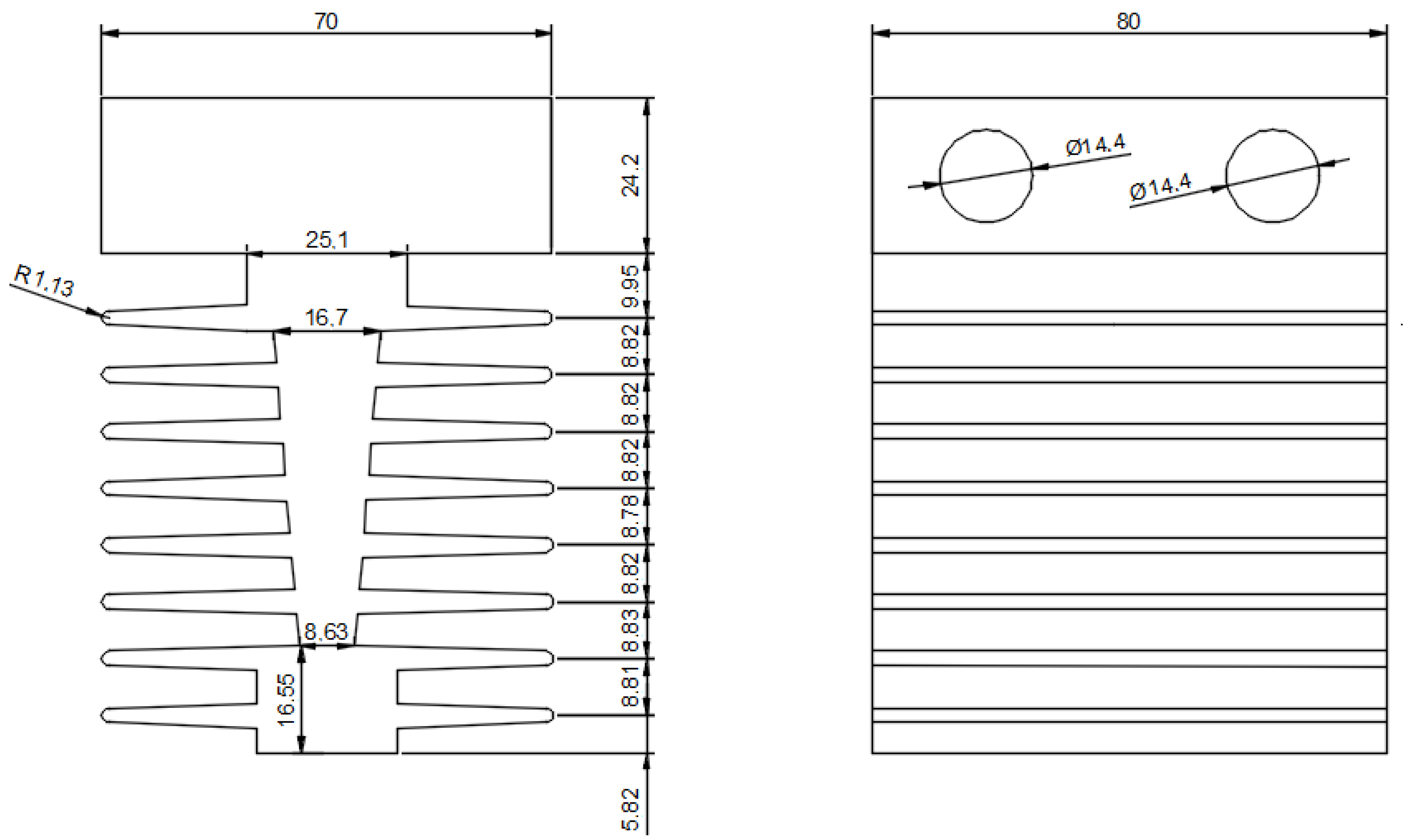
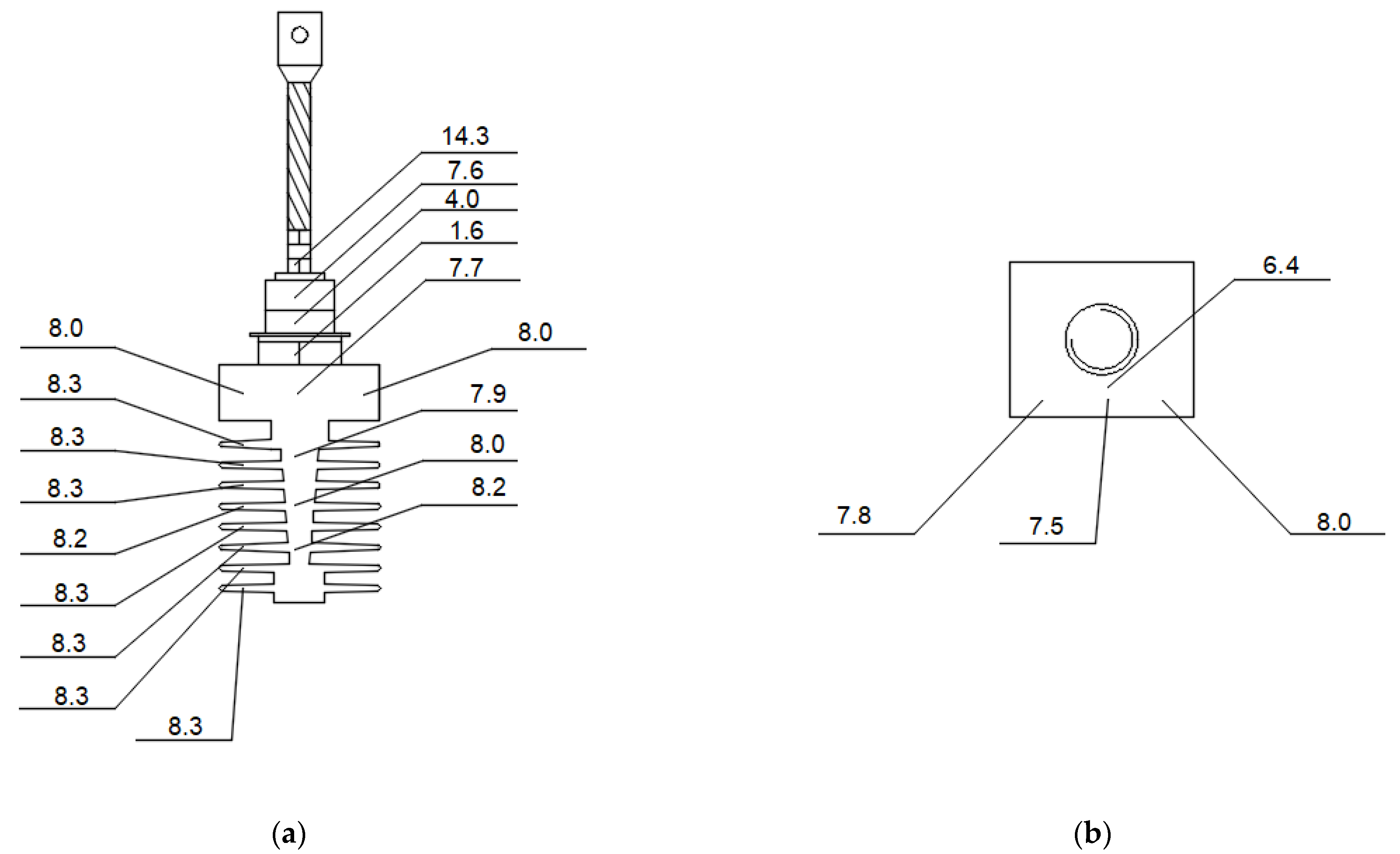
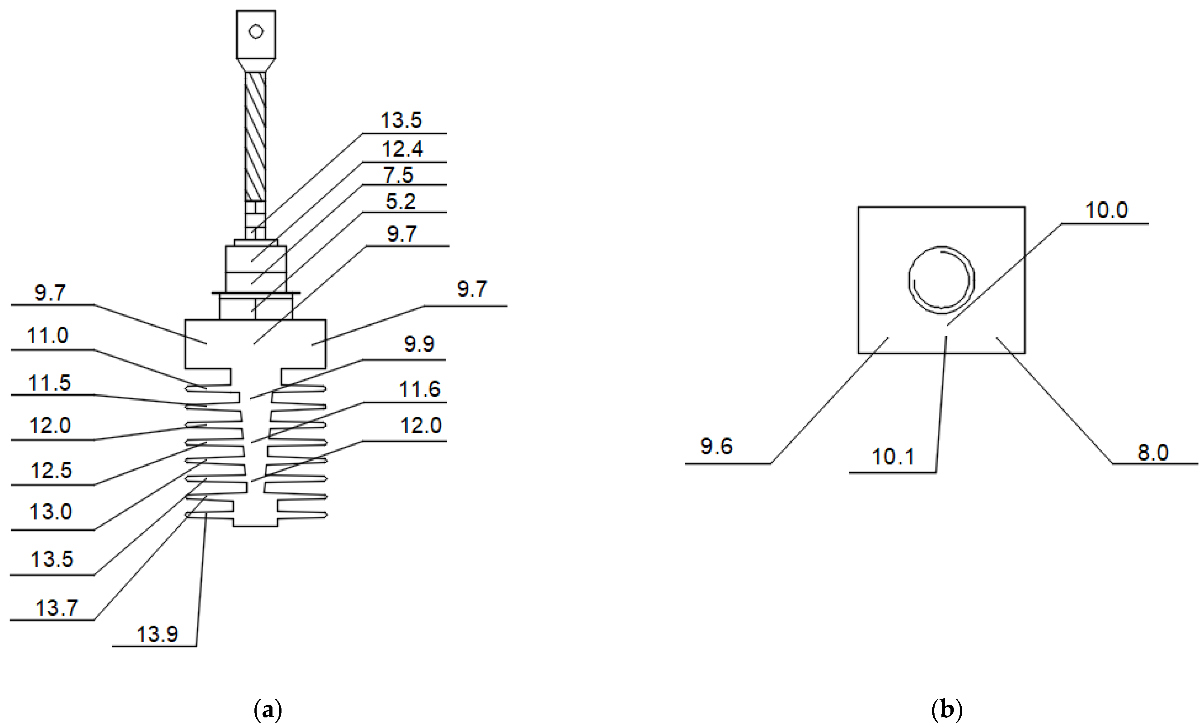
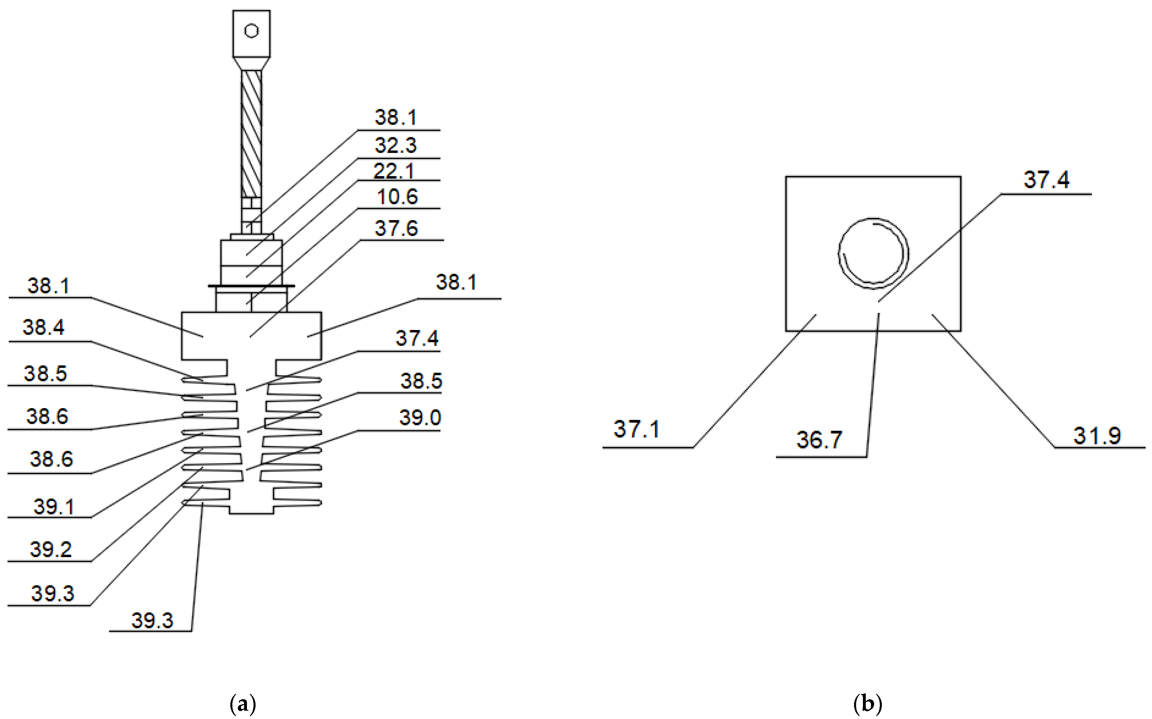
Figure 1.
The dimensions of the used heat sink (in mm).


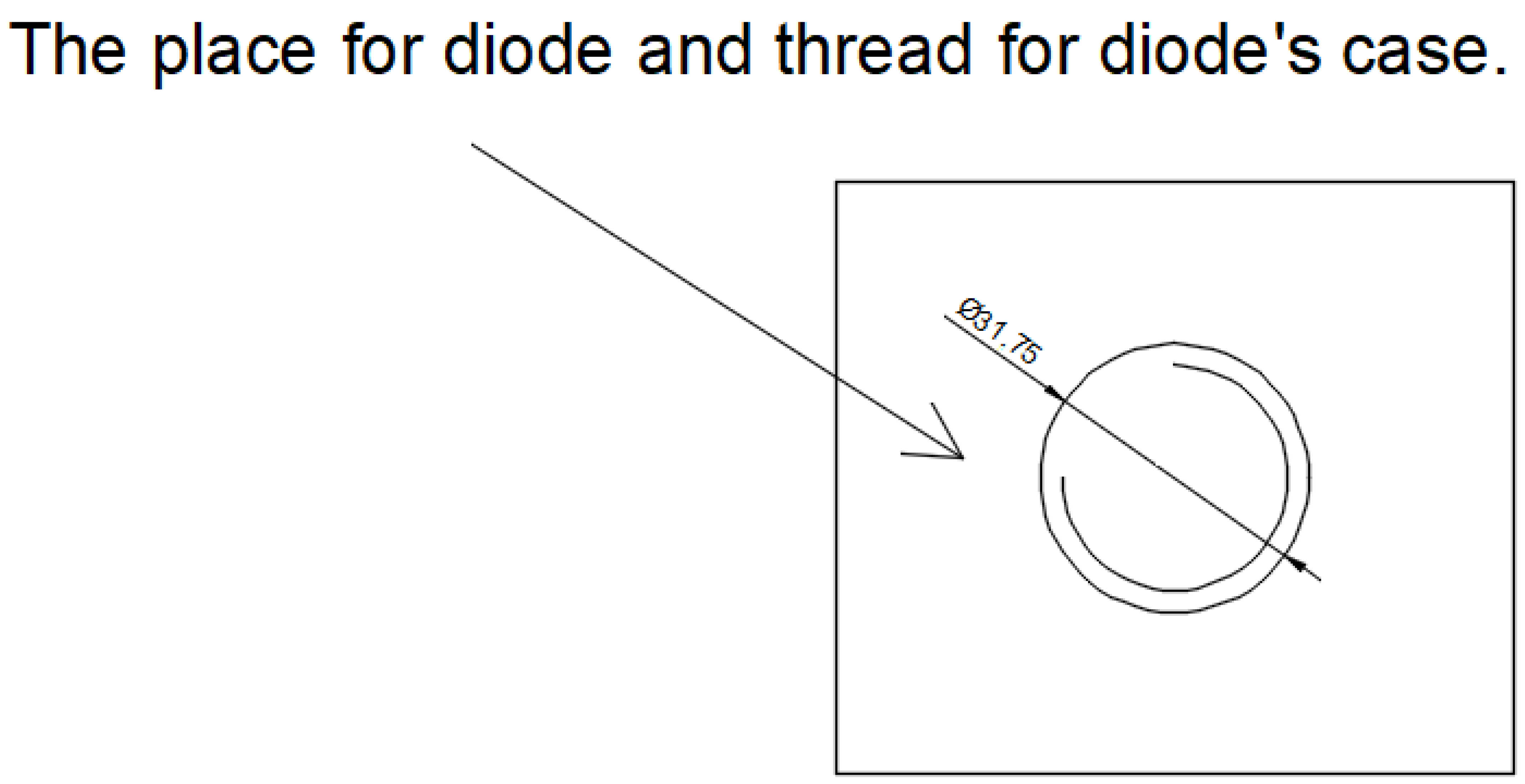
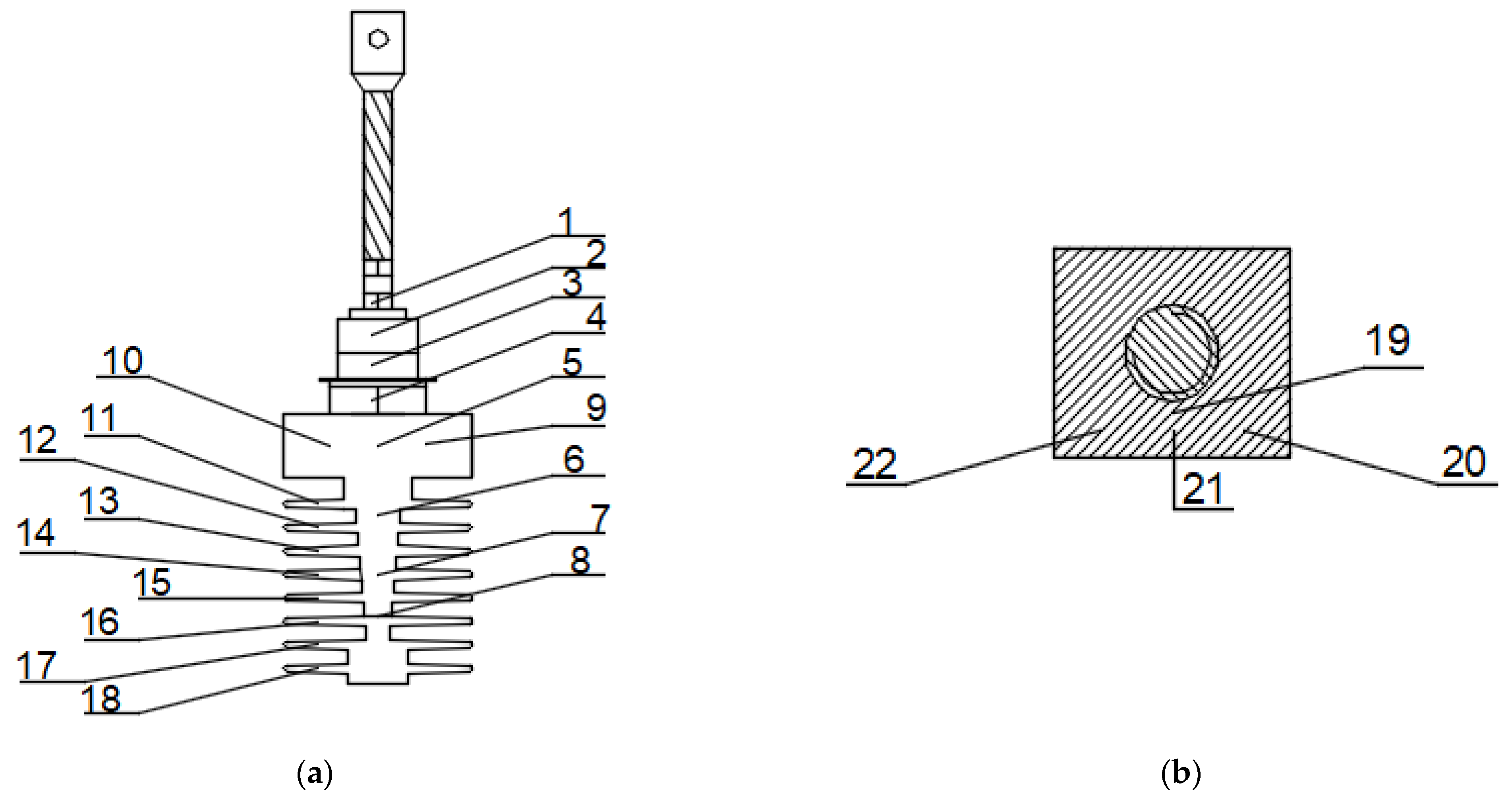
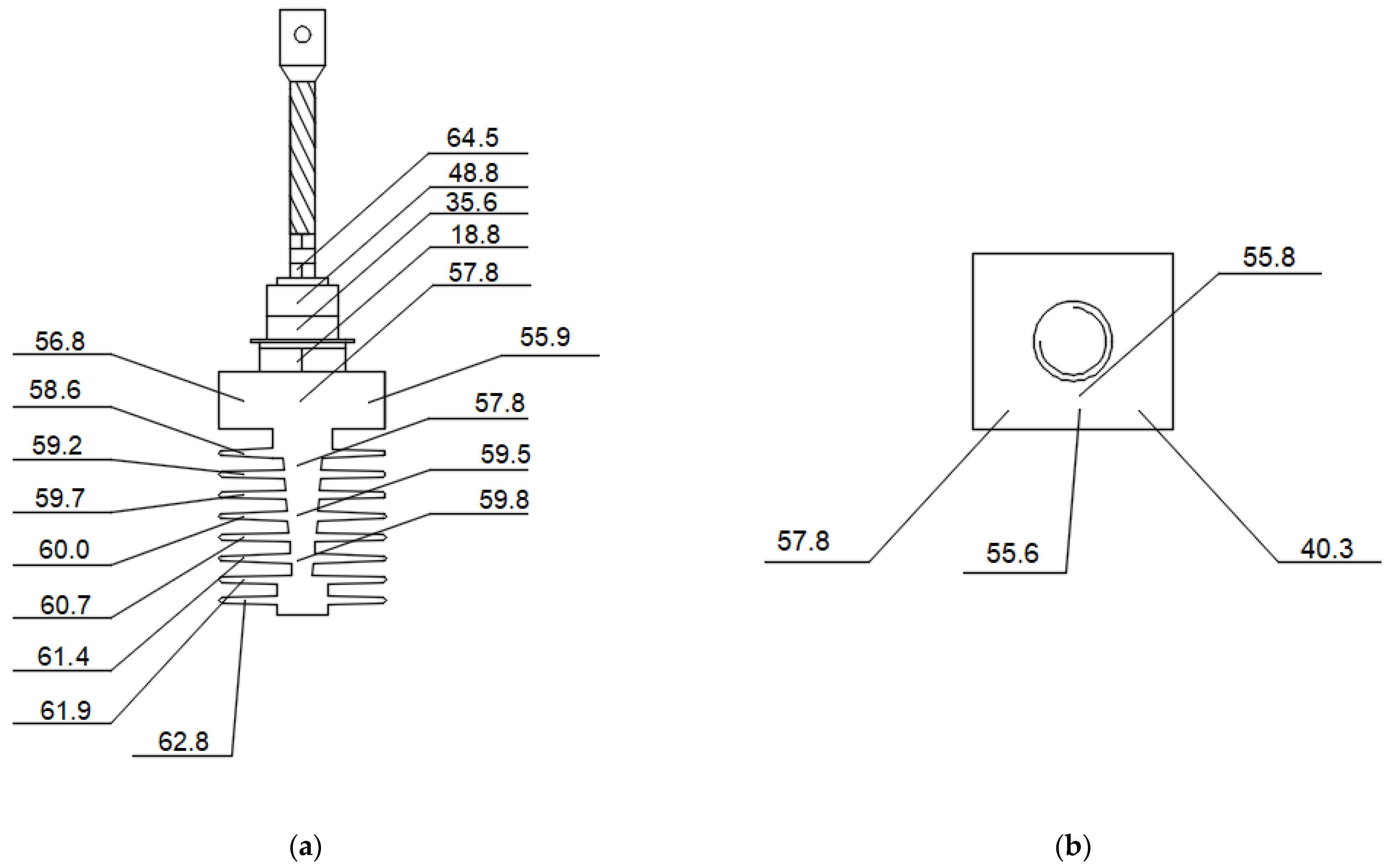
Figure 2.
The locations of the markers on the diode case and on the heat sink surface: (a) side view; (b) top view of the heat sink.
Figure 2.
The locations of the markers on the diode case and on the heat sink surface: (a) side view; (b) top view of the heat sink.

Figure 3.
Scheme of the measuring system.

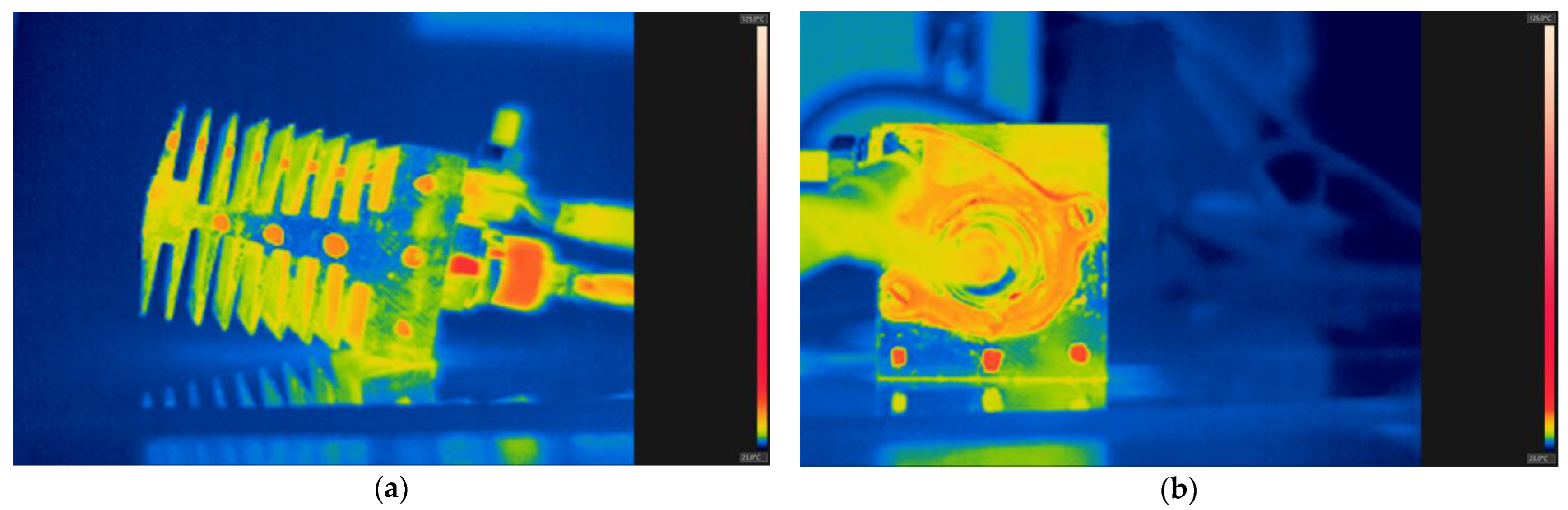
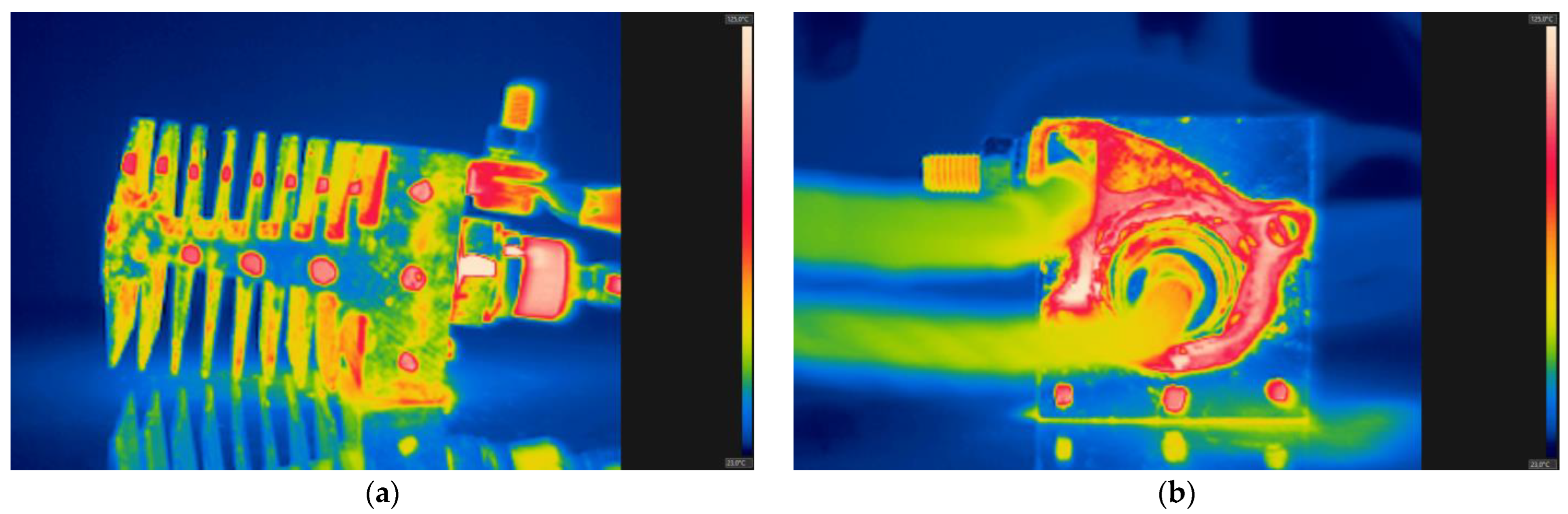
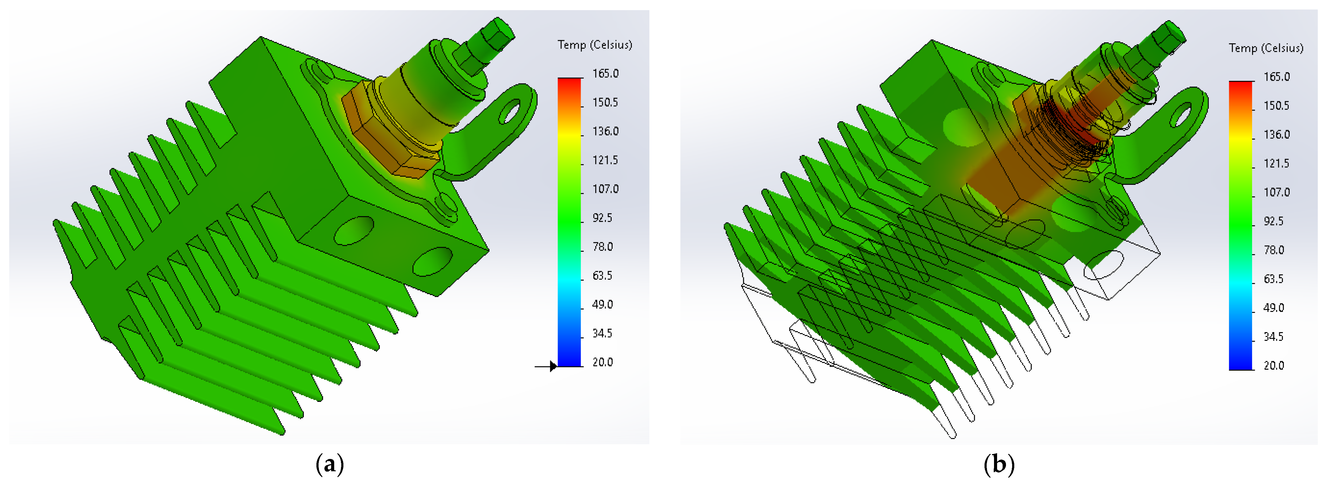
Figure 4.
The thermograms showing the heat sink for a power of Pj = 11.56 W: (a) side view; (b) top view. The temperature on the thermogram ranges from 23 °C to 125 °C.
Figure 4.
The thermograms showing the heat sink for a power of Pj = 11.56 W: (a) side view; (b) top view. The temperature on the thermogram ranges from 23 °C to 125 °C.

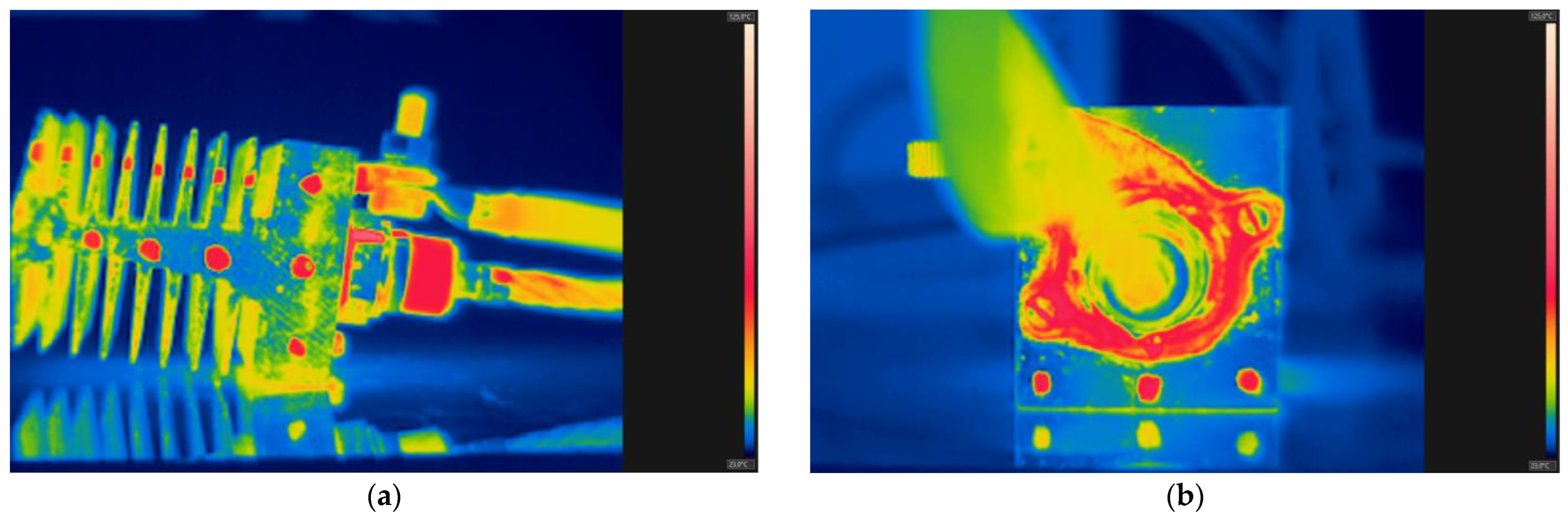
Figure 5.
The thermograms showing a heat sink for a power of Pj = 28.80 W: (a) side view; (b) top view. The temperature on the thermogram ranges from 23 °C to 125 °C.
Figure 5.
The thermograms showing a heat sink for a power of Pj = 28.80 W: (a) side view; (b) top view. The temperature on the thermogram ranges from 23 °C to 125 °C.

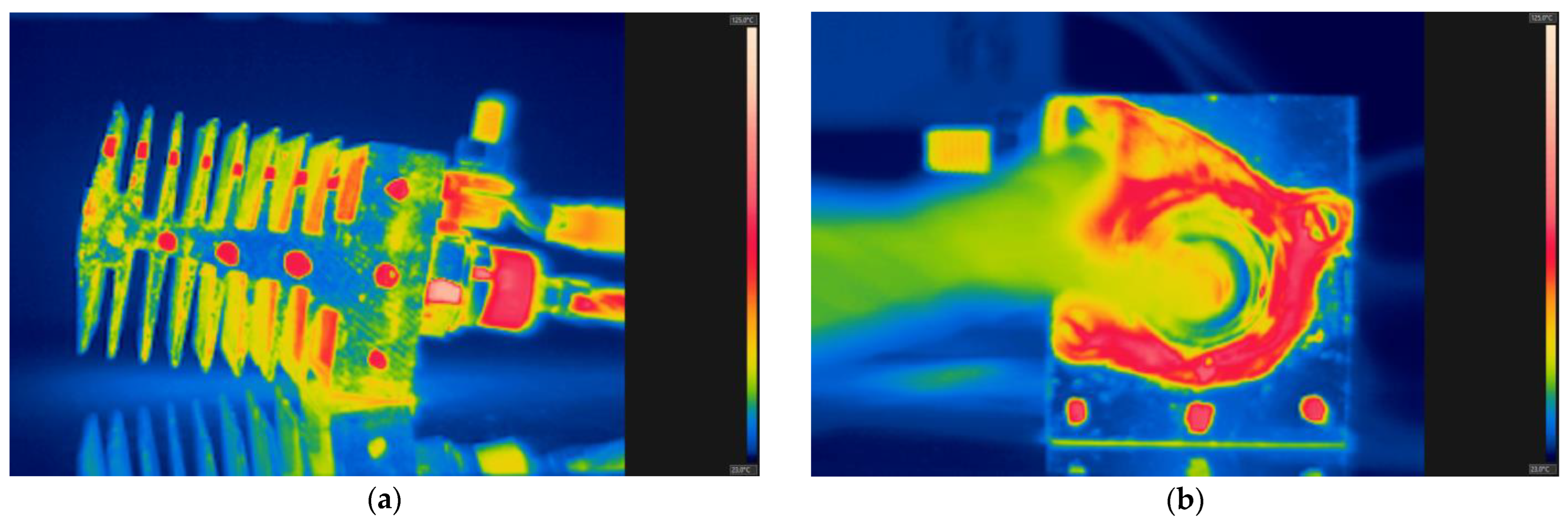
Figure 6.
The thermograms showing a heat sink for a power of Pj = 49.61 W: (a) side view; (b) top view. The temperature on the thermogram ranges from 23 °C to 125 °C.
Figure 6.
The thermograms showing a heat sink for a power of Pj = 49.61 W: (a) side view; (b) top view. The temperature on the thermogram ranges from 23 °C to 125 °C.

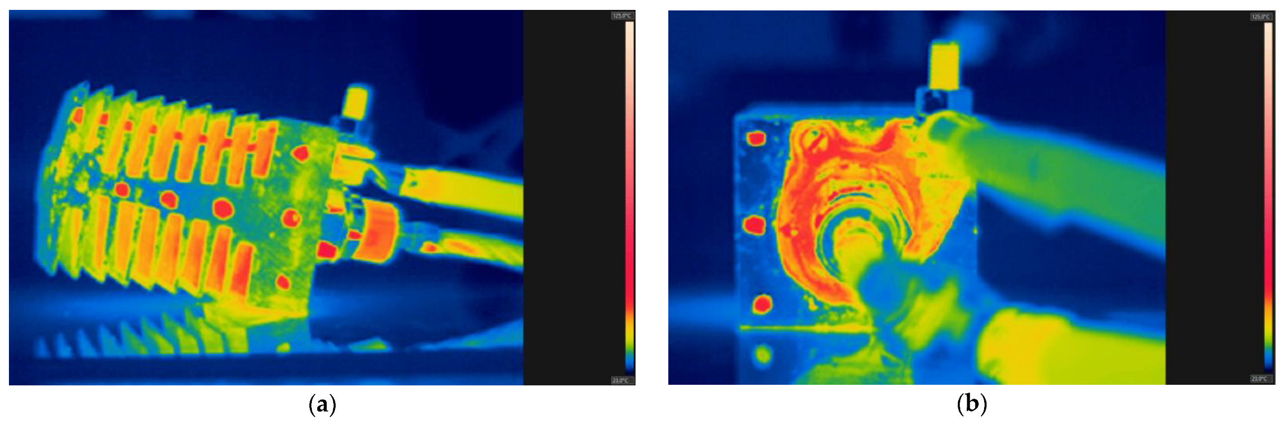
Figure 7.
The thermograms showing a heat sink for a power of Pj = 74.36 W: (a) side view; (b) top view. The temperature on the thermogram ranges from 23 °C to 125 °C.
Figure 7.
The thermograms showing a heat sink for a power of Pj = 74.36 W: (a) side view; (b) top view. The temperature on the thermogram ranges from 23 °C to 125 °C.

Figure 8.
The thermograms showing a heat sink for a power of Pj = 117.99 W: (a) side view; (b) top view. The temperature on the thermogram ranges from 23 °C to 125 °C.
Figure 8.
The thermograms showing a heat sink for a power of Pj = 117.99 W: (a) side view; (b) top view. The temperature on the thermogram ranges from 23 °C to 125 °C.

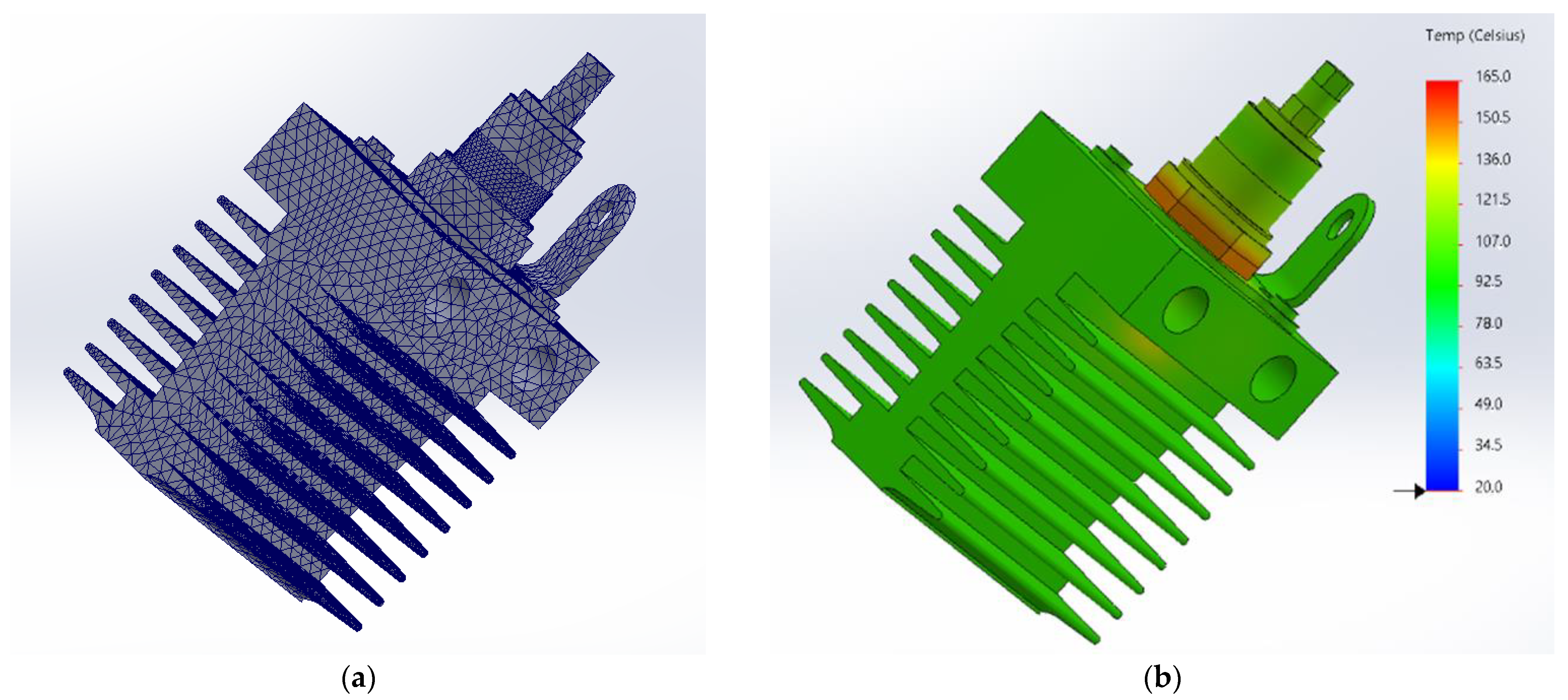
Figure 9.
(a) The view of the diode model for the smallest mesh element value of 1.0 mm. (b) The simulation result for the smallest mesh element value of 1.0 mm (ts = 280 s; Tj = 162.8 °C; Pj = 117.99 W; the temperature ranges from 20 °C to 165 °C).
Figure 9.
(a) The view of the diode model for the smallest mesh element value of 1.0 mm. (b) The simulation result for the smallest mesh element value of 1.0 mm (ts = 280 s; Tj = 162.8 °C; Pj = 117.99 W; the temperature ranges from 20 °C to 165 °C).

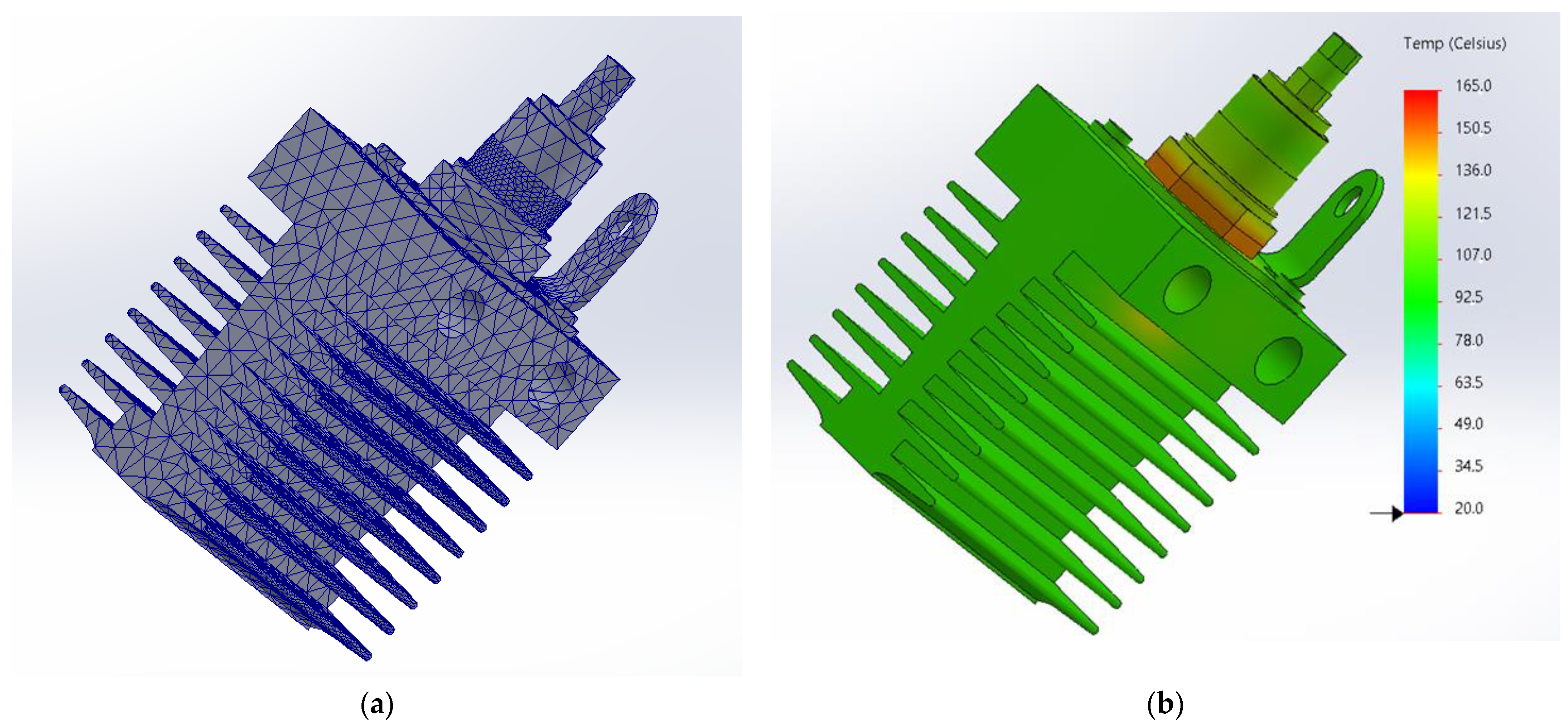
Figure 10.
(a) The view of the diode model for the smallest mesh element value of 2.5 mm. (b) The simulation result for the smallest mesh element value of 2.5 mm (ts = 65 s; Tj = 162.7 °C; Pj = 117.99 W; the temperature ranges from 20 °C to 165 °C).
Figure 10.
(a) The view of the diode model for the smallest mesh element value of 2.5 mm. (b) The simulation result for the smallest mesh element value of 2.5 mm (ts = 65 s; Tj = 162.7 °C; Pj = 117.99 W; the temperature ranges from 20 °C to 165 °C).

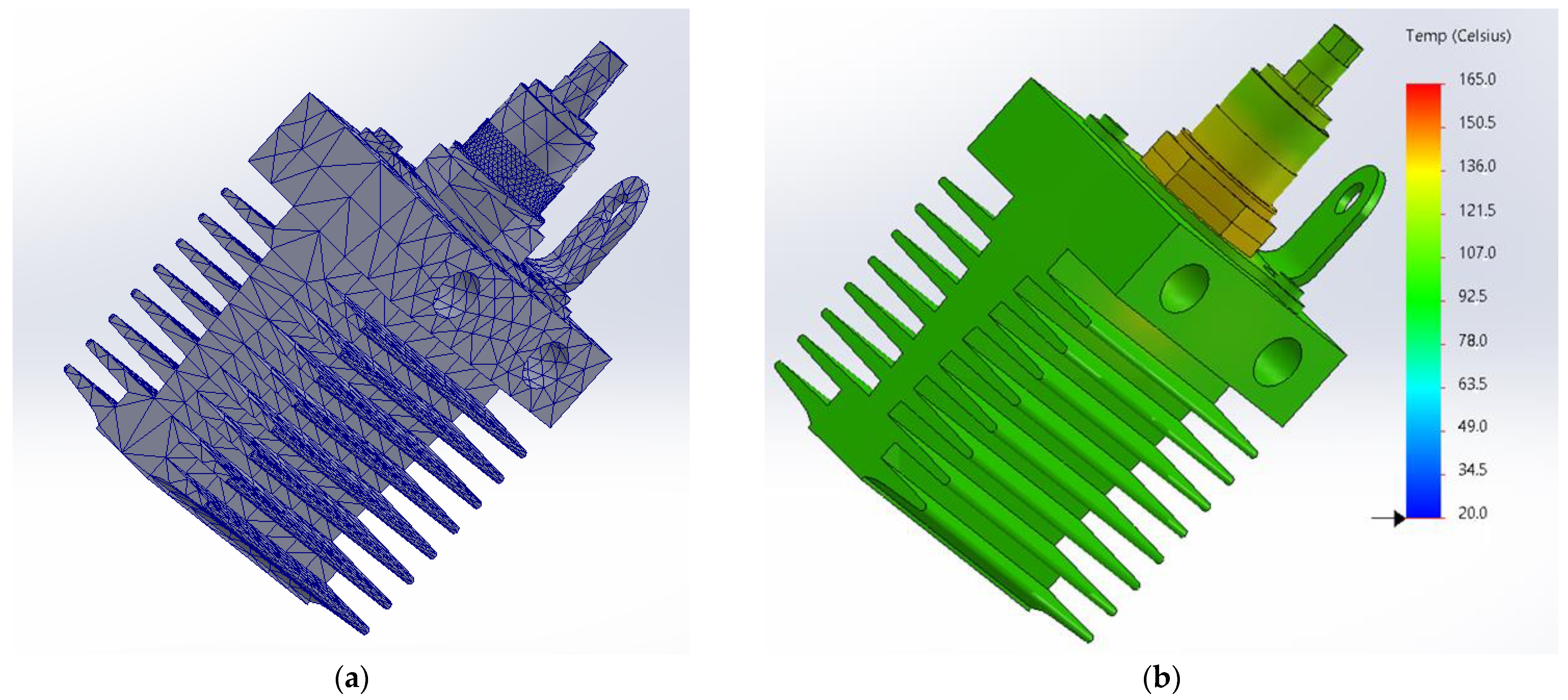
Figure 11.
(a) The view of the diode model for the smallest mesh element value of 5.5 mm. (b) The simulation result for the smallest mesh element value of 5.5 mm (ts = 12 s; Tj = 150.5 °C; Pj = 117.99 W; the temperature ranges from 20 °C to 165 °C).
Figure 11.
(a) The view of the diode model for the smallest mesh element value of 5.5 mm. (b) The simulation result for the smallest mesh element value of 5.5 mm (ts = 12 s; Tj = 150.5 °C; Pj = 117.99 W; the temperature ranges from 20 °C to 165 °C).

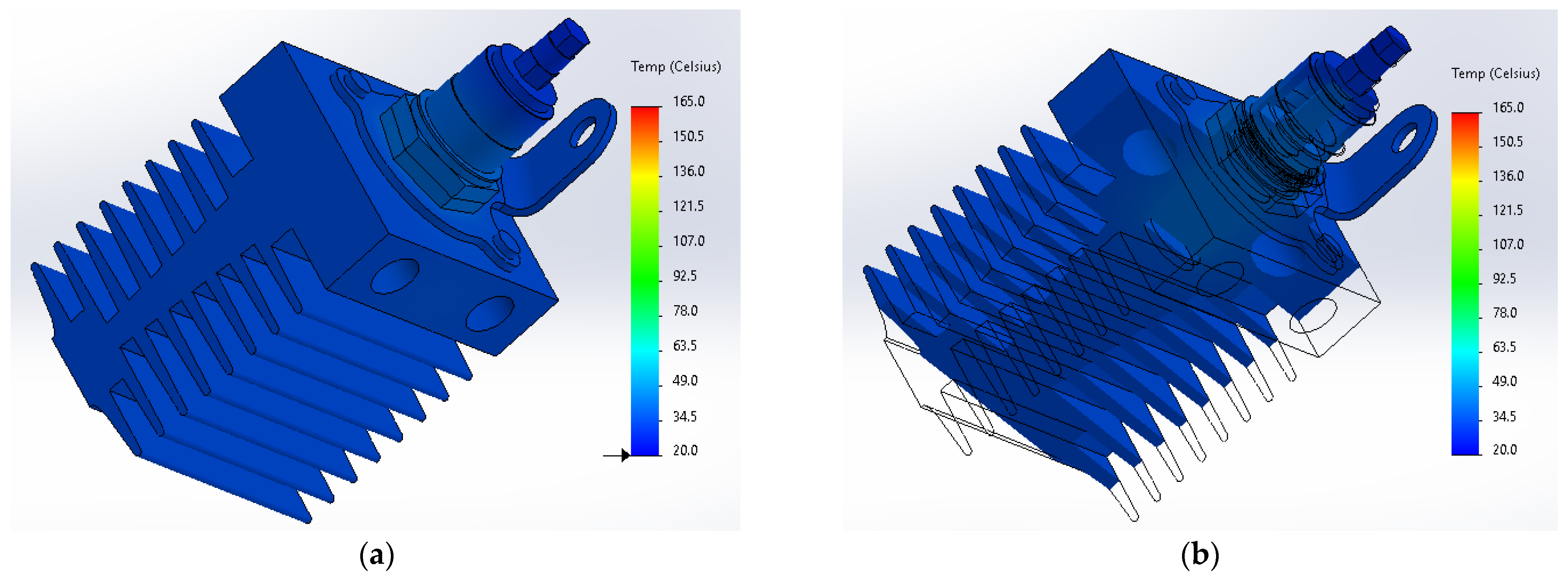
Figure 12.
The simulation result showing the heat sink for a power of Pj = 11.56 W: (a) side view; (b) cross section. The temperature ranges from 20 °C to 165 °C.
Figure 12.
The simulation result showing the heat sink for a power of Pj = 11.56 W: (a) side view; (b) cross section. The temperature ranges from 20 °C to 165 °C.

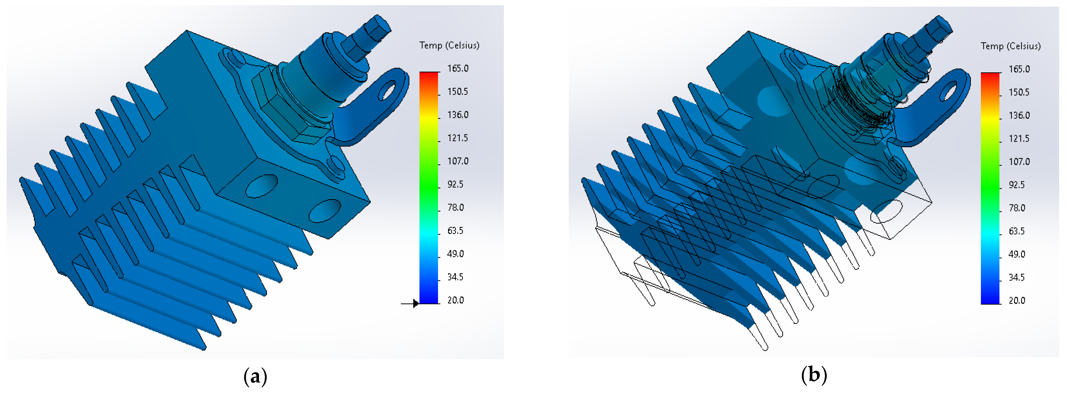
Figure 13.
The simulation result showing the heat sink for a power of Pj = 28.80 W: (a) side view; (b) cross section. The temperature ranges from 20 °C to 165 °C.
Figure 13.
The simulation result showing the heat sink for a power of Pj = 28.80 W: (a) side view; (b) cross section. The temperature ranges from 20 °C to 165 °C.

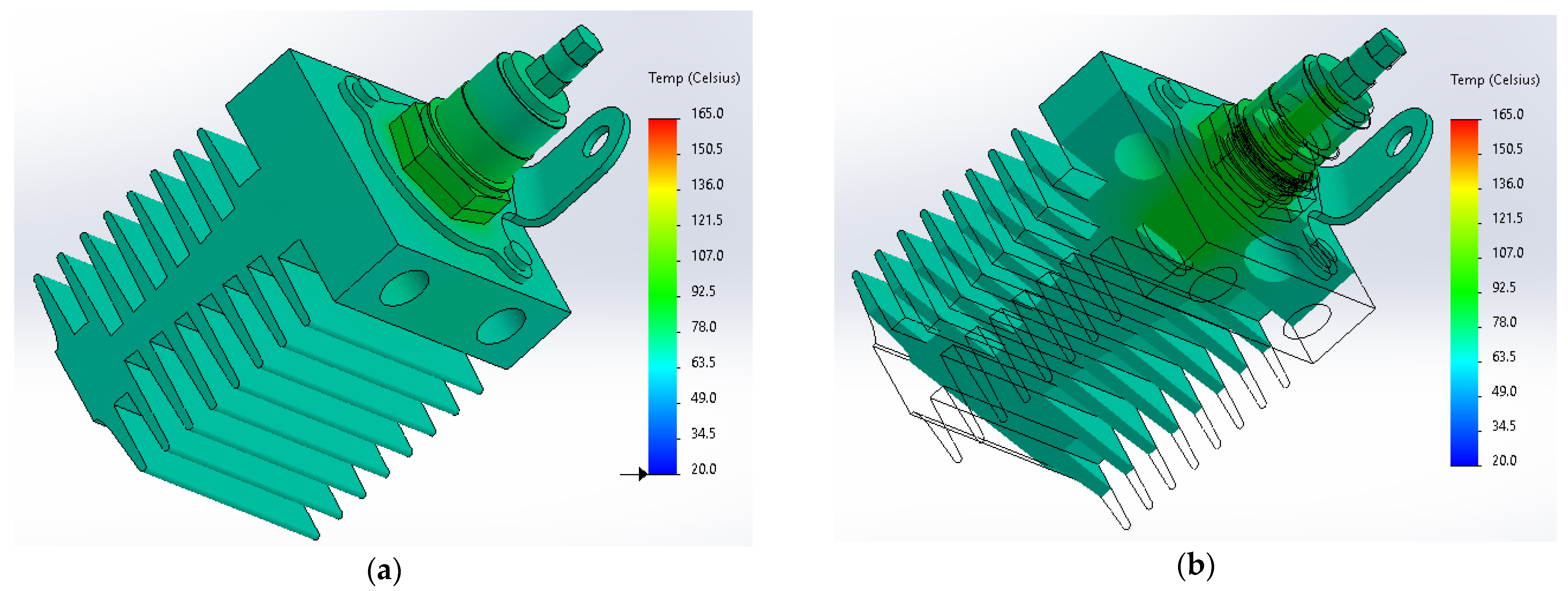
Figure 14.
The simulation result showing the heat sink for a power of Pj = 49.61 W: (a) side view; (b) cross section. The temperature ranges from 20 °C to 165 °C.
Figure 14.
The simulation result showing the heat sink for a power of Pj = 49.61 W: (a) side view; (b) cross section. The temperature ranges from 20 °C to 165 °C.

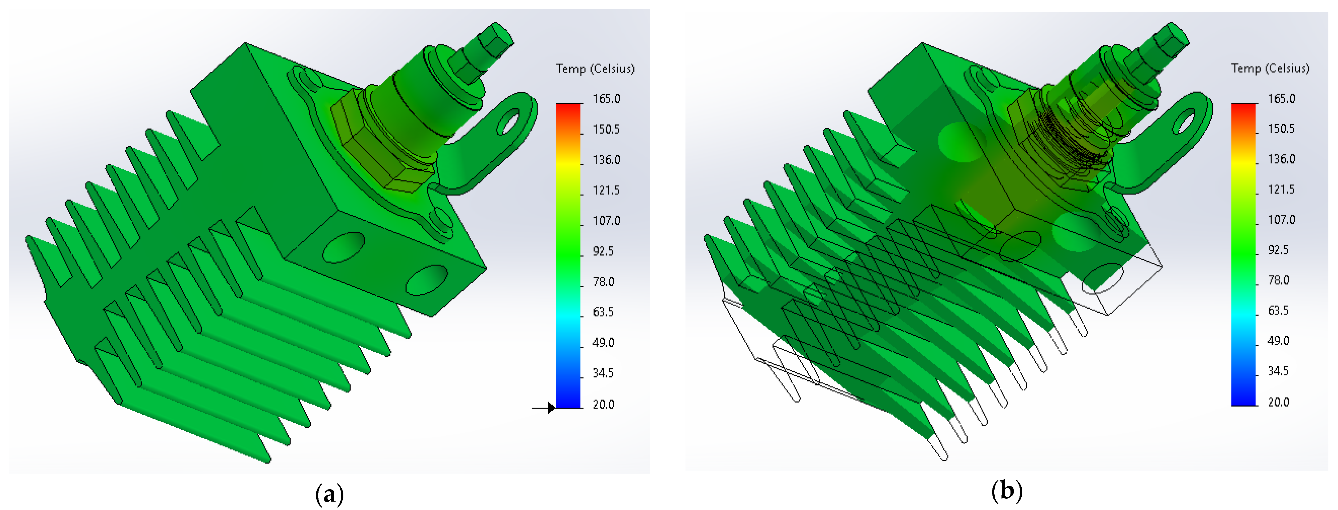
Figure 15.
The simulation result showing the heat sink for a power of Pj = 74.36 W: (a) side view; (b) cross section. The temperature ranges from 20 °C to 165 °C.
Figure 15.
The simulation result showing the heat sink for a power of Pj = 74.36 W: (a) side view; (b) cross section. The temperature ranges from 20 °C to 165 °C.

Figure 16.
The simulation result showing the heat sink for a power of Pj = 117.99 W: (a) side view; (b) cross section. The temperature ranges from 20 °C to 165 °C.
Figure 16.
The simulation result showing the heat sink for a power of Pj = 117.99 W: (a) side view; (b) cross section. The temperature ranges from 20 °C to 165 °C.

Figure 17.
Differences (Tj − Ts) between the junction temperature (Tj) and the surface temperatures (TS) (from Table 6 and Table 7) at points presented in Figure 2 for a power of Pj = 11.56 W: (a) side view; (b) top view.

Figure 18.
Differences (Tj − Ts) between the junction temperature (Tj) and the surface temperatures (TS) (from Table 6 and Table 7) at points presented in Figure 2 for a power of Pj = 28.80 W: (a) side view; (b) top view.

Figure 19.
Differences (Tj − Ts) between the junction temperature (Tj) and the surface temperatures (TS) (from Table 6 and Table 7) at points presented in Figure 2 for a power of Pj = 49.61 W: (a) side view; (b) top view.

Figure 20.
Differences (Tj − Ts) between the junction temperature (Tj) and the surface temperatures (TS) (from Table 6 and Table 7) at points presented in Figure 2 for a power of Pj = 74.36 W: (a) side view; (b) top view.

Figure 21.
Differences (Tj − Ts) between the junction temperature (Tj) and the surface temperatures (TS) (from Table 6 and Table 7) at points presented in Figure 2 for a power of Pj = 117.99 W: (a) side view; (b) top view.


Table 1.
The values of coefficients a and b from Equation (18).
| Shape | alam | blam | aturb | bturb | |
|---|---|---|---|---|---|
| Vertical flat wall | 109 | 0.59 | 0.25 | 0.129 | 0.33 |
| Upper flat wall | 108 | 0.54 | 0.25 | 0.14 | 0.33 |
| Lower flat wall | 105 | 0.25 | 0.25 | Na | Na |
Table 2.
The values of the ε and hc coefficients selected for each of the points presented in Figure 2 for Pj = 11.56 W, Pj = 28.80 W and Pj = 49.61 W.
Table 2.
The values of the ε and hc coefficients selected for each of the points presented in Figure 2 for Pj = 11.56 W, Pj = 28.80 W and Pj = 49.61 W.
| Point Number | Pj = 11.56 (W) | Pj = 28.80 (W) | Pj = 49.61 (W) | ||||
|---|---|---|---|---|---|---|---|
| Material | [-] | hc [-] | [-] | hc [-] | [-] | hc [-] | |
| 1 | Polished aluminum | 0.12 | 10.35 | 0.12 | 13.74 | 0.11 | 16.34 |
| 2 | Porcelain | 0.90 | 7.28 | 0.90 | 27.32 | 0.87 | 32.13 |
| 3 | Oxidized aluminum | 0.07 | 24.72 | 0.07 | 20.94 | 0. 07 | 24.92 |
| 4 | Copper | 0.09 | 20.11 | 0.09 | 22.65 | 0.09 | 26.79 |
| 5 | Old aluminum | 0.44 | 19.10 | 0.24 | 22.36 | 0.21 | 25.42 |
| 6 | Old aluminum | 0.44 | 19.20 | 0.24 | 22.48 | 0.21 | 25.63 |
| 7 | Old aluminum | 0.44 | 19.16 | 0.24 | 22.40 | 0.21 | 25.43 |
| 8 | Old aluminum | 0.44 | 19.10 | 0.24 | 22.31 | 0.21 | 25.27 |
| 9 | Old aluminum | 0.44 | 32.23 | 0.24 | 37.75 | 0.21 | 42.91 |
| 10 | Old aluminum | 0.44 | 32.12 | 0.24 | 37.59 | 0.21 | 43.21 |
| 11 | Old aluminum | 0.44 | 31.65 | 0.24 | 37.01 | 0.21 | 42.29 |
| 12 | Old aluminum | 0.44 | 35.65 | 0.24 | 41.71 | 0.21 | 47.49 |
| 13 | Old aluminum | 0.44 | 36.70 | 0.24 | 42.90 | 0.21 | 48.81 |
| 14 | Old aluminum | 0.44 | 37.57 | 0.24 | 43.90 | 0.21 | 49.93 |
| 15 | Old aluminum | 0.44 | 38.57 | 0.24 | 44.74 | 0.21 | 50.88 |
| 16 | Old aluminum | 0.44 | 38.30 | 0.24 | 44.19 | 0.21 | 50.44 |
| 17 | Old aluminum | 0.44 | 33.13 | 0.24 | 38.49 | 0.21 | 43.80 |
| 18 | Old aluminum | 0.44 | 32.97 | 0.24 | 38.10 | 0.21 | 43.90 |
| 19 | Old aluminum | 0.44 | 74.18 | 0.24 | 86.50 | 0.21 | 99.34 |
| 20 | Old aluminum | 0.44 | 72.61 | 0.24 | 88.77 | 0.21 | 100.50 |
| 21 | Old aluminum | 0.44 | 74.07 | 0.24 | 87.01 | 0.21 | 99.82 |
| 22 | Old aluminum | 0.44 | 73.95 | 0.24 | 87.01 | 0.21 | 99.78 |
Table 3.
The values of the ε and hc coefficients selected for each of the points presented in Figure 2 for Pj = 74.36 W and Pj = 117.99 W.
Table 3.
The values of the ε and hc coefficients selected for each of the points presented in Figure 2 for Pj = 74.36 W and Pj = 117.99 W.
| Point Number | Pj = 74.36 (W) | Pj = 117.99 (W) | |||
|---|---|---|---|---|---|
| Material | [-] | hc [-] | [-] | hc [-] | |
| 1 | Polished aluminum | 0.11 | 17.07 | 0.11 | 18.21 |
| 2 | Porcelain | 0.87 | 34.74 | 0.87 | 37.38 |
| 3 | Oxidized aluminum | 0.07 | 26.37 | 0.07 | 28.61 |
| 4 | Copper | 0.09 | 28.76 | 0.09 | 31.02 |
| 5 | Old aluminum | 0.18 | 27.20 | 0.16 | 29.50 |
| 6 | Old aluminum | 0.18 | 27.36 | 0.16 | 29.58 |
| 7 | Old aluminum | 0.18 | 27.20 | 0.16 | 29.26 |
| 8 | Old aluminum | 0.18 | 27.02 | 0.16 | 29.08 |
| 9 | Old aluminum | 0.18 | 46.00 | 0.16 | 49.95 |
| 10 | Old aluminum | 0.18 | 45.70 | 0.16 | 49.76 |
| 11 | Old aluminum | 0.18 | 45.21 | 0.16 | 48.72 |
| 12 | Old aluminum | 0.18 | 50.64 | 0.16 | 54.74 |
| 13 | Old aluminum | 0.18 | 51.95 | 0.16 | 56.07 |
| 14 | Old aluminum | 0.18 | 53.24 | 0.16 | 57.58 |
| 15 | Old aluminum | 0.18 | 54.17 | 0.16 | 58.13 |
| 16 | Old aluminum | 0.18 | 53.74 | 0.16 | 57.68 |
| 17 | Old aluminum | 0.18 | 46.35 | 0.16 | 49.97 |
| 18 | Old aluminum | 0.18 | 45.98 | 0.16 | 49.75 |
| 19 | Old aluminum | 0.18 | 105.57 | 0.16 | 114.36 |
| 20 | Old aluminum | 0.18 | 107.05 | 0.16 | 117.91 |
| 21 | Old aluminum | 0.18 | 105.94 | 0.16 | 114.90 |
| 22 | Old aluminum | 0.18 | 105.85 | 0.16 | 113.94 |
Table 4.
The temperature values obtained from TS simulations and TC measurements for each of the points presented in Figure 2 for Pj = 11.56 W, Pj = 28.80 W and Pj = 49.61 W.
Table 4.
The temperature values obtained from TS simulations and TC measurements for each of the points presented in Figure 2 for Pj = 11.56 W, Pj = 28.80 W and Pj = 49.61 W.
| Point Number | Pj = 11.56 (W) | Pj = 28.80 (W) | Pj = 49.61 (W) | |||
|---|---|---|---|---|---|---|
| TS (°C) | TC (°C) | TS (°C) | TC (°C) | TS (°C) | TC (°C) | |
| 1 | 28.8 | 28.3 | 45.9 | 45.8 | 70.7 | 71.6 |
| 2 | 35.5 | 36.3 | 47.0 | 47.3 | 72.0 | 72.2 |
| 3 | 39.1 | 37.8 | 51.9 | 51.2 | 78.3 | 76.5 |
| 4 | 41.5 | 41.6 | 54.2 | 54.7 | 87.8 | 87.9 |
| 5 | 35.4 | 35.2 | 49.7 | 48.6 | 68.9 | 67.7 |
| 6 | 35.2 | 35.5 | 49.5 | 49.2 | 68.8 | 69.3 |
| 7 | 35.1 | 35.4 | 47.8 | 48.8 | 68.0 | 67.8 |
| 8 | 34.9 | 35.2 | 47.4 | 48.3 | 67.8 | 66.6 |
| 9 | 35.1 | 35.4 | 49.7 | 49.0 | 68.2 | 68.4 |
| 10 | 35.1 | 35.2 | 49.7 | 48.5 | 68.3 | 69.8 |
| 11 | 34.8 | 35.5 | 48.4 | 48.6 | 68.1 | 68.7 |
| 12 | 34.8 | 35.4 | 47.9 | 48.5 | 68.1 | 67.9 |
| 13 | 34.8 | 35.3 | 47.4 | 48.6 | 68.0 | 67.9 |
| 14 | 34.9 | 35.3 | 46.9 | 48.5 | 68.0 | 67.7 |
| 15 | 34.8 | 35.2 | 46.4 | 47.5 | 67.8 | 66.0 |
| 16 | 34.8 | 35.3 | 45.9 | 47.1 | 67.4 | 66.0 |
| 17 | 34.8 | 35.1 | 45.7 | 47.5 | 66.9 | 66.1 |
| 18 | 34.8 | 34.8 | 45.5 | 46.4 | 66.7 | 64.8 |
| 19 | 36.7 | 35.8 | 49.4 | 49.2 | 69.1 | 70.8 |
| 20 | 35.1 | 34.5 | 51.4 | 52.4 | 72.3 | 73.2 |
| 21 | 35.6 | 35.7 | 49.3 | 49.9 | 69.9 | 71.8 |
| 22 | 35.3 | 35.6 | 49.8 | 49.9 | 69.8 | 71.7 |
Table 5.
The temperature values obtained from TS simulations and TC measurements for each of the points presented in Figure 2 for Pj = 74.36 W and Pj = 117.99 W.
Table 5.
The temperature values obtained from TS simulations and TC measurements for each of the points presented in Figure 2 for Pj = 74.36 W and Pj = 117.99 W.
| Point Number | Pj = 74.36 (W) | Pj = 117.99 (W) | ||
|---|---|---|---|---|
| TS (°C) | TC (°C) | TS (°C) | TC (°C) | |
| 1 | 83.1 | 81.5 | 98.2 | 99.5 |
| 2 | 88.9 | 91.3 | 113.9 | 115.6 |
| 3 | 99.1 | 98.5 | 127.1 | 128.7 |
| 4 | 110.6 | 110.2 | 143.9 | 142.2 |
| 5 | 83.6 | 82.5 | 104.9 | 106.6 |
| 6 | 83.8 | 84.0 | 104.9 | 107.5 |
| 7 | 82.7 | 82.5 | 103.2 | 103.7 |
| 8 | 82.2 | 80.9 | 102.9 | 101.7 |
| 9 | 83.1 | 83.9 | 106.8 | 108.9 |
| 10 | 83.1 | 82.3 | 105,9 | 107.5 |
| 11 | 82.8 | 83.6 | 104.1 | 105.8 |
| 12 | 82.7 | 81.9 | 103.5 | 104.5 |
| 13 | 82.6 | 81.5 | 103.0 | 103.4 |
| 14 | 82.6 | 81.7 | 102.7 | 104.4 |
| 15 | 82.1 | 79.1 | 102.0 | 98.4 |
| 16 | 82.0 | 79.3 | 101.3 | 98.7 |
| 17 | 81.9 | 77.8 | 100.8 | 98.0 |
| 18 | 81.5 | 76.0 | 99.9 | 96.7 |
| 19 | 83.8 | 84.8 | 106.9 | 109.2 |
| 20 | 89.3 | 88.5 | 122.4 | 120.8 |
| 21 | 84.5 | 85.7 | 107.1 | 110.9 |
| 22 | 84.1 | 85.5 | 104.9 | 107.9 |
Table 6.
The differences between the junction temperature (Tj) and the temperatures at the points shown in Figure 2 (TS) for Pj = 11.56 W, Pj = 28.80 W and Pj = 49.61 W.
Table 6.
The differences between the junction temperature (Tj) and the temperatures at the points shown in Figure 2 (TS) for Pj = 11.56 W, Pj = 28.80 W and Pj = 49.61 W.
| Point Number | Pj = 11.56 (W) | Pj = 28.80 (W) | Pj = 49.61 (W) | ||||||
|---|---|---|---|---|---|---|---|---|---|
| Tj (°C) | TS (°C) | Tj − TS (°C) | Tj (°C) | TS (°C) | Tj − TS (°C) | Tj (°C) | TS (°C) | Tj − TS (°C) | |
| 1 | 43.1 | 28.8 | 14.3 | 59.4 | 45.9 | 13.5 | 94.9 | 70.7 | 24.2 |
| 2 | 43.1 | 35.5 | 7.6 | 59.4 | 47.0 | 12.4 | 94.9 | 72.0 | 22.9 |
| 3 | 43.1 | 39.1 | 4.0 | 59.4 | 51.9 | 7.5 | 94.9 | 78.3 | 16.6 |
| 4 | 43.1 | 41.5 | 1.6 | 59.4 | 54.2 | 5.2 | 94.9 | 87.8 | 7.1 |
| 5 | 43.1 | 35.4 | 7.7 | 59.4 | 49.7 | 9.7 | 94.9 | 68.9 | 26.0 |
| 6 | 43.1 | 35.2 | 7.9 | 59.4 | 49.5 | 9.9 | 94.9 | 68.8 | 26.1 |
| 7 | 43.1 | 35.1 | 8.0 | 59.4 | 47.8 | 11.6 | 94.9 | 68.0 | 26.9 |
| 8 | 43.1 | 34.9 | 8.2 | 59.4 | 47.4 | 12.0 | 94.9 | 67.8 | 27.1 |
| 9 | 43.1 | 35.1 | 8.0 | 59.4 | 49.7 | 9.7 | 94.9 | 68.2 | 26.7 |
| 10 | 43.1 | 35.1 | 8.0 | 59.4 | 49.7 | 9.7 | 94.9 | 68.3 | 26.6 |
| 11 | 43.1 | 34.8 | 8.3 | 59.4 | 48.4 | 11.0 | 94.9 | 68.1 | 26.8 |
| 12 | 43.1 | 34.8 | 8.3 | 59.4 | 47.9 | 11.5 | 94.9 | 68.1 | 26.8 |
| 13 | 43.1 | 34.8 | 8.3 | 59.4 | 47.4 | 12.0 | 94.9 | 68.0 | 26.9 |
| 14 | 43.1 | 34.9 | 8.2 | 59.4 | 46.9 | 12.5 | 94.9 | 68.0 | 26.9 |
| 15 | 43.1 | 34.8 | 8.3 | 59.4 | 46.4 | 13.0 | 94.9 | 67.8 | 27.1 |
| 16 | 43.1 | 34.8 | 8.3 | 59.4 | 45.9 | 13.5 | 94.9 | 67.4 | 27.5 |
| 17 | 43.1 | 34.8 | 8.3 | 59.4 | 45.7 | 13.7 | 94.9 | 66.9 | 28.0 |
| 18 | 43.1 | 34.8 | 8.3 | 59.4 | 45.5 | 13.9 | 94.9 | 66.7 | 28.2 |
| 19 | 43.1 | 36.7 | 6.4 | 59.4 | 49.4 | 10.0 | 94.9 | 69.1 | 25.8 |
| 20 | 43.1 | 35.1 | 8.0 | 59.4 | 51.4 | 8.0 | 94.9 | 72.3 | 22.6 |
| 21 | 43.1 | 35.6 | 7.5 | 59.4 | 49.3 | 10.1 | 94.9 | 69.9 | 25.0 |
| 22 | 43.1 | 35.3 | 7.8 | 59.4 | 49.8 | 9.6 | 94.9 | 69.8 | 25.1 |
Table 7.
The differences between the junction temperature (Tj) and the temperatures at the points shown in Figure 2 (TS) for Pj = 74.36 W and Pj = 117.99 W.
Table 7.
The differences between the junction temperature (Tj) and the temperatures at the points shown in Figure 2 (TS) for Pj = 74.36 W and Pj = 117.99 W.
| Point Number | Tj = 74.36 (W) | Pj = 117.99 (W) | ||||
|---|---|---|---|---|---|---|
| Tj (°C) | TS (°C) | Tj − TS (°C) | Tj (°C) | TS (°C) | Tj − TS (°C) | |
| 1 | 121.2 | 83.1 | 38.1 | 162.7 | 98.2 | 64.5 |
| 2 | 121.2 | 88.9 | 32.3 | 162.7 | 113.9 | 48.8 |
| 3 | 121.2 | 99.1 | 22.1 | 162.7 | 127.1 | 35.6 |
| 4 | 121.2 | 110.6 | 10.6 | 162.7 | 143.9 | 18.8 |
| 5 | 121.2 | 83.6 | 37.6 | 162.7 | 104.9 | 57.8 |
| 6 | 121.2 | 83.8 | 37.4 | 162.7 | 104.9 | 57.8 |
| 7 | 121.2 | 82.7 | 38.5 | 162.7 | 103.2 | 59.5 |
| 8 | 121.2 | 82.2 | 39.0 | 162.7 | 102.9 | 59.8 |
| 9 | 121.2 | 83.1 | 38.1 | 162.7 | 106.8 | 55.9 |
| 10 | 121.2 | 83.1 | 38.1 | 162.7 | 105,9 | 56.8 |
| 11 | 121.2 | 82.8 | 38.4 | 162.7 | 104.1 | 58.6 |
| 12 | 121.2 | 82.7 | 38.5 | 162.7 | 103.5 | 59.2 |
| 13 | 121.2 | 82.6 | 38.6 | 162.7 | 103.0 | 59.7 |
| 14 | 121.2 | 82.6 | 38.6 | 162.7 | 102.7 | 60.0 |
| 15 | 121.2 | 82.1 | 39.1 | 162.7 | 102.0 | 60.7 |
| 16 | 121.2 | 82.0 | 39.2 | 162.7 | 101.3 | 61.4 |
| 17 | 121.2 | 81.9 | 39.3 | 162.7 | 100.8 | 61.9 |
| 18 | 121.2 | 81.5 | 39.7 | 162.7 | 99.9 | 62.8 |
| 19 | 121.2 | 83.8 | 37.4 | 162.7 | 106.9 | 55.8 |
| 20 | 121.2 | 89.3 | 31.9 | 162.7 | 122.4 | 40.3 |
| 21 | 121.2 | 84.5 | 36.7 | 162.7 | 107.1 | 55.6 |
| 22 | 121.2 | 84.1 | 37.1 | 162.7 | 104.9 | 57.8 |
Disclaimer/Publisher’s Note: The statements, opinions and data contained in all publications are solely those of the individual author(s) and contributor(s) and not of MDPI and/or the editor(s). MDPI and/or the editor(s) disclaim responsibility for any injury to people or property resulting from any ideas, methods, instructions or products referred to in the content. |
© 2022 by the authors. Licensee MDPI, Basel, Switzerland. This article is an open access article distributed under the terms and conditions of the Creative Commons Attribution (CC BY) license (https://creativecommons.org/licenses/by/4.0/).
Share and Cite
MDPI and ACS Style
Dziarski, K.; Hulewicz, A.; Drużyński, Ł.; Dombek, G. Indirect Thermographic Temperature Measurement of a Power-Rectifying Diode Die Based on a Heat Sink Thermogram. Energies 2023, 16, 332. https://doi.org/10.3390/en16010332
AMA Style
Dziarski K, Hulewicz A, Drużyński Ł, Dombek G. Indirect Thermographic Temperature Measurement of a Power-Rectifying Diode Die Based on a Heat Sink Thermogram. Energies. 2023; 16(1):332. https://doi.org/10.3390/en16010332
Chicago/Turabian StyleDziarski, Krzysztof, Arkadiusz Hulewicz, Łukasz Drużyński, and Grzegorz Dombek. 2023. "Indirect Thermographic Temperature Measurement of a Power-Rectifying Diode Die Based on a Heat Sink Thermogram" Energies 16, no. 1: 332. https://doi.org/10.3390/en16010332
Note that from the first issue of 2016, this journal uses article numbers instead of page numbers. See further details here.