
LCL Filter Parameter and Hardware Design Methodology for Minimum Volume Considering Capacitor Lifetimes
by
 , , , and
Pedro C. Bolsi
1,2,* ,
,
Edemar O. Prado
1,2,
Hamiltom C. Sartori
2,
João Manuel Lenz
1 and
José Renes Pinheiro
1,2 1
LABEFEA, Federal University of Bahia, Salvador 40210-630, BA, Brazil
2
GEPOC, Federal University of Santa Maria, Santa Maria 97105-900, RS, Brazil
*
Author to whom correspondence should be addressed.
Energies 2022, 15(12), 4420; https://doi.org/10.3390/en15124420
Submission received: 19 May 2022
/
Revised: 8 June 2022
/
Accepted: 14 June 2022
/
Published: 17 June 2022
(This article belongs to the Special Issue Advances in Power Electronic Converters with Application in Renewable Energy Sources)
Abstract
:A design methodology for minimum volume of LCL filters applied to grid connected converters is proposed. It combines the determination of filter parameter values (inductances and capacitances) to hardware design (component technology and inductor construction). Using the proposed strategy, different combinations of L-C-L that meet standard restrictions are determined. The influence of the harmonic content that results from filter design is considered in order to estimate component losses, and filter and bus capacitor lifetimes. Results are presented for filters that lead to the smallest volume, highest capacitor lifetime, or a compromise between both. A case study with three different magnetic material technologies and two types of capacitors is done. The design methodology is experimentally validated for a 1 kW converter. Step-by-step procedures for the determination of filter parameters and inductor hardware design are provided.
1. Introduction
Be it for renewable energy generation or uninterruptible power sources, the use of pulse-width modulated power converters enables the synthesis of voltages with low harmonic distortion. These converters operate at switching frequencies well above the fundamental of Hz [1,2]. Switching produces high frequency harmonics that must be attenuated to avoid disturbances to other loads connected to the grid. Therefore, there are specific standards that determine the harmonic injection limits [3,4,5].
The use of passive filters is common for the mitigation of harmonic currents at switching frequency, well above the control system active range. However, due to their low attenuation rate, purely inductive filters (L) may result in large and heavy components, because a high inductive reactance is needed; which also leads to a high voltage drop [6]. For these motives, the use of LCL filters becomes attractive due to their reduced component dimensions. The main disadvantage associated to LCL filters is the instability caused by the resonance of filter elements, demanding some sort of damping [7,8,9,10].
The definition of the electrical parameters of the LCL inductance and capacitance is not a trivial task. Based on a limit of harmonic injection determined by the standard, the LCL filter design methodologies are diverse [1,2,6,7,8,9,11,12,13,14,15]. The most common strategy consists of setting a fixed value for the filter capacitance (), usually chosen as a value equal to or below 5% of the base capacitance (), and to design the converter () and grid () side inductors with a ratio “r” between them. This ratio is sometimes adjusted to achieve a desired filter performance [8,11,16].
A slightly different approach is to set and determine for a desired current ripple (I) at the converter input, calculating using the ratio “r” [6,7,9,14]. Similarly, it is also possible to design to obtain a certain harmonic current amplitude at the switching frequency [12]. Other methodologies of designing LCL filters may include modeling the system using the extended harmonic domain [2], using filter transfer functions [6,13], or employing genetic algorithms [17].
With respect to the component design, a discussion on the relation of losses to the inductance value, including damping losses, was done by [1], where it was shown that there is a minimum value for the inductance of the LCL filter to minimize losses. Another work [18], seeks to optimize the relationship between losses and volume, taking into consideration the temperature of the magnetic materials. However, neither authors have evaluated the impact of the technologies they used on the losses and volume, which are decisive to the design. In [16] the use of different magnetic material technologies for the LCL filter is studied, but not from a design methodology perspective. In [19] a design methodology for the LCL filter including EMI consideration is presented; nanocrystalline cores are chosen among four materials, but no comparative analysis among component designs is included.
In the aforementioned works that analyzed the LCL filter considering component design, none have considered the influence of the filter design on the capacitors, despite the fact that the current ripple on the converter side influences the losses and lifetime of the filter and DC bus capacitors () [20]. On the other hand, works that discuss capacitor lifetime do not do it in conjunction with the parametric and hardware design of the filter. These works aim to evaluate the capacitor lifetime using mission profiles [20,21], or seek optimization of volume, cost, reliability, and losses, making use of linearized models of the physical characteristics of the capacitors [22].
This way, the literature on the subject lacks design methodologies that propose to optimize the parametric LCL filter design (values of L and C) in light of losses, volume and capacitor lifetime; discussing the advantages and disadvantages from decisions in the parametric design; considering the impact on the hardware and addressing the used technologies.
A common objective for optimization is cost [23,24,25,26], for competitive market reasons. However, component cost has periodical and local variations, involving non-deterministic variables that depend of technological development, competition among manufacturers, geopolitical factors, availability, and market segment. This way, the obtained results in a cost optimization may be localized, and not applicable to other situations. On the other hand, volume and loss optimization can be more useful, and employed in different situations, permitting an ideal compromise among design variables.
With this in mind, this work employs a design methodology based on the sweeping of values, and of the amplitude of the switching frequency harmonic current in (converter-side). Based on the specifications of the converter and normative restrictions, numerous combinations of L-C-L are found by sweeping. The discretion of possible solutions is made by analyzing the hardware design of each component, considering the use of different technologies, present on a database. With the converter waveforms, losses and temperature in each component are estimated, as well as the lifetimes of capacitors and . With this, the objective is to, while meeting normative restrictions, minimize filter volume, maximize capacitor lifetimes, or find a suitable compromise between both. The design methodology is summarized in Figure 1.
The parametric design is validated by waveform measurement, demonstrating compliance to the adopted standard. The hardware design is validated by loss measurement, since it is dependent on their adequate estimation.
2. Filter Parametric Design
As a case study, the input stage of a double-conversion uninterruptible power source (UPS) will be analyzed, as illustrated in Figure 2. This UPS topology consists of two converters connected back-to-back: a rectifier in the input stage, which regulates DC bus voltage and corrects power factor; and an inverter on the output stage, which provides a sinusoidal voltage to the load [27].
As mentioned, the LCL filter is designed to meet the restrictions of injected harmonics into the grid. In this work, the IEC 61000-3-4 standard [5] is considered. The LCL filter is designed per-phase, since this topology allows the converter to be split into three single-phase half-bridge converters. The L-C-L values are determined using the transfer function of the filter.
In order to find an optimal design considering losses, volume and capacitor lifetimes, the developed methodology performs a sweep of filter capacitance () values and of harmonic current amplitudes () on the converter-side inductor (). The purpose of this sweep is to explore the filter design possibilities considering normative limits, while not being restricted to a predetermined value of current ripple and/or filter capacitance. The reduction of filter volume is evaluated in light of a possible compromise with capacitor lifetimes.
The developed methodology does not consider the presence of grid inductance nor of an input transformer, since these are typically unknowns. Therefore, the filter is designed for a grid without any inductive characteristic, meeting by itself the restrictions determined by the adopted standard. Otherwise, the grid and transformer leakage inductances would add to the grid-side inductor ().
2.1. Converter-Side Inductor
With a phase-shifted PWM modulation, the expression for the converter-side voltage () comprises its DC and fundamental components, as well as its switching harmonics and side lobes. The LCL filter is designed to attenuate the highest amplitude harmonic generated by the converter, which occurs at the switching frequency ():
at which is the bus voltage, the modulation index, and a zero order Bessel function. Disregarding voltage drops on the inductors, can be determined by:
where is the grid voltage (RMS value).
Assuming a Thévenin equivalent circuit in which and are part of the grid impedance, the value of can be determined using the transfer function of an L filter:
where is replaced by from (1), and is replaced by the amplitude of the current harmonic of at the switching frequency (), which is varied by the sweep.
2.2. Grid-Side Inductor
The grid-side inductor is designed to attenuate the remaining harmonics that are not filtered by and . The transfer function of the LCL filter with passive damping is used:
at which is the value of the damping resistor, once more is replaced by , and is replaced by its highest harmonic amplitude ().
The value of is determined using the limit of admissible harmonic current, set by the standard. It is specified in terms of the ratio between the amplitudes of the switching frequency to the low frequency current: . For IEC 61000-3-4, must be ≤0.6%.
The dependence of with regards to , and is shown in (4). is related to the resonant frequency (), which must be between 10 times the low frequency and 0.5 times the switching frequency [6,7]:
Since and are both unknowns, the procedure of obtaining the value of is iterative. As a starting point, can be assumed. is calculated by (6) and used in (4) to estimate . Then, and are re-calculated, and (4) is used once more. With the second estimate of , and are adjusted with (5) and (6). This procedure reduces the need for iterations of and , that must be repeated until the desired attenuation of is obtained.
The main drawback of LCL filters is its instability, caused by the resonance of its elements. Several works have approached this subject, proposing resonance damping passively [1,2,6,7,14,18], actively [8,9,10,11,12,28,29], or without any damping [13]. In spite of passive damping resulting in ohmic losses, in this work it was adopted because of its robustness and simplicity.
The developed methodology results in a set of , and that meet standard restrictions. Given a converter with the specifications shown in Table 1, the resulting inductances are illustrated in Figure 3, for a sweep of from 1.8% to 6.7% of . The values of and are plotted as a function of normalized with respect to the amplitude of the low frequency component (). This ratio is varied from 7% to 27%. The values chosen for the sweep of and may vary according to the rated power of the converter and component availability. In Figure 3, the inverse proportion of and is observed, and how the increase of reduces the value of required to meet the standard.
3. Filter Hardware Design
Typically, LCL filter design methodologies are limited to the determination of electrical parameters of capacitance and inductance. These are seldom considered in conjunction with the technologies that will be used to construct the filter. The process of designing the components involves adequately modeling the particular characteristics of each technology. The combined analysis of the parametric and hardware design is proposed, in order to determine the optimal relation or compromise for LCL filter losses and volume, and capacitor lifetimes of and .
3.1. Inductor Sizing
In the developed methodology, different magnetic material technologies are considered for the construction of the inductors. To determine the volume and losses of the LCL filter inductors, the design is performed considering three magnetic core technologies for and : non-grain oriented silicon steel (NGO steel) [30], for its low cost and high magnetic flux density; Kool Mµ [31], for its relatively high magnetic flux density, but lower core losses than silicon steel; and 3C92 ferrite [32], for its low magnetic losses.
A database is built to compare the design of each inductor using these technologies. It contains 21 sizes of NGO steel sheet (EI geometry), with lengths ranging from 14 mm to 300 mm; 35 sizes of Kool Mµ core (toroid geometry), considering up to 5 stacked cores, totaling 175 possible core sizes, with relative magnetic permeabilities ranging from 26 to 125; and 28 sizes of 3C92 ferrite (EE geometry), considering up to 5 stacked cores, totaling 140 possible solutions. For conductors, solid copper wires are considered for and stranded wire for , because the latter operates with high frequency.
A step-by-step procedure for the design of each inductor is shown in Appendix A. By using the proposed strategy for inductor sizing, their design will be limited by temperature rise, as a function of copper and core losses. As an indirect consequence of designing the inductors for the smallest possible volume, as is intended in the proposed methodology, when considering losses and heating, the inductor must also have low losses, in order to limit temperature rise.
3.2. Capacitor Losses and Lifetime
To achieve an optimized LCL filter, it is necessary that the capacitors be designed considering metrics that go beyond the traditional approach of simply defining the total required capacitance. While the capacitor losses can be used as a metric, a more useful parameter is the estimated capacitor lifetime. This allows a design choice that brings the best cost-benefit considering the system lifetime, since capacitors are notoriously known for being one of the electronic components most prone to failure [33].
The capacitor loss model is approximated by considering only its equivalent series resistance (ESR). This value is obtained from manufacturer datasheets, valid for steady state operation, and is a function of the frequency. The ESR is multiplied by the capacitor current harmonic spectrum, and by summing the individual contribution of each harmonic, the total electrical loss in the capacitor is obtained. Thus, for both and , losses () and temperature () are determined as:
where is the RMS amplitude of the ith current harmonic and its corresponding ESR, that varies with temperature. is the total thermal resistance of the capacitor, given by the manufacturer, and the ambient temperature. When there are capacitors in parallel in the DC bus, the current is split.
Since losses and temperature are interdependent, and are determined iteratively. The initial temperature used to determine is ; with this value, the are determined, and is calculated, with which a new is estimated; this process is repeated until the change in between iterations is below 1%. Only the thermal equilibrium state is analyzed.
The to be considered in the loss and lifetime calculations will depend on the positioning of heat sources around the converter and filter, and the type of cooling system employed. This determination is complex and beyond the scope of this work. With this in mind, it is assumed that only natural convection is present and that C.
One of the main reasons for capacitor failure is the degradation of its dielectric, caused by voltage and temperature stresses building up over time. Thus, it is possible to estimate lifetime using a parameterized model, created from statistical failure data for each component under stress conditions [20,34].
Each capacitor technology has particular characteristics that influence its behavior in terms of losses and lifetime. For the hardware of the filter, film capacitors (C4AF series [35]) are chosen, due to its advantages in terms of cost and volume. For similar reasons, electrolytic capacitors (Type DCMC [36]) are chosen for the DC bus.
Given a determined electrothermal stress, the lifetime () of the film capacitor is [20]:
where is the rated lifetime of the film capacitor, and its rated voltage and temperature, the voltage over , and its voltage stress coefficient.
The lifetime () of an electrolytic capacitor () is [20]:
where is the rated lifetime for the electrolytic capacitor, its rated temperature, its rated voltage, the voltage over , the voltage stress factor, the capacitor current, the rated current, the temperature rise at , and the temperature stress coefficient. Only the nominal voltage and power levels were considered for the UPS system.
4. Application of the Proposed Methodology
To demonstrate the combination of the LCL filter parametric (Section 2) and hardware (Section 3) design methodologies, the converter specifications from Table 1 and the values of , and shown in Figure 3 are used. The design of each component is addressed in the following sections.
4.1. Filter Inductors and
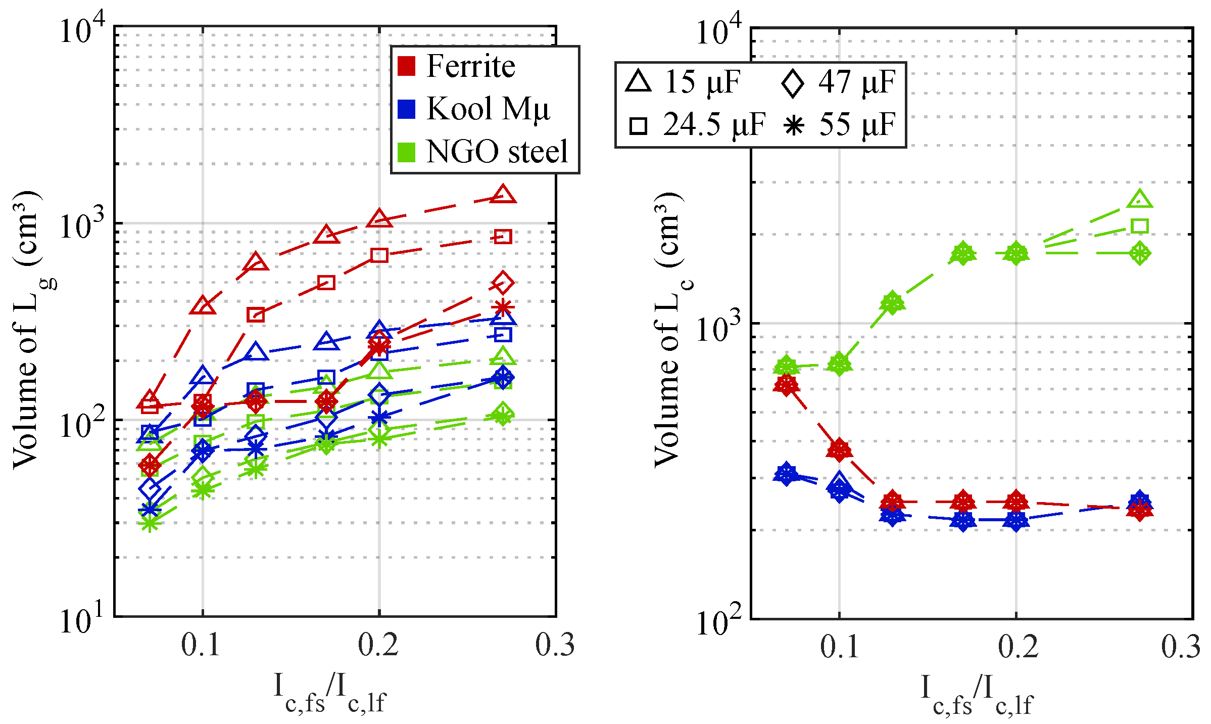
The volumes of and , for each magnetic material technology (NGO Steel, Kool Mµ and 3C92 ferrite) are presented in Figure 4. The technologies are being identified for each point of and . Similar to the behavior of inductance shown in Figure 3, the volumes for tend to increase as gets higher, with larger volumes associated to smaller capacitances for . For , the volumes tend to reduce as gets higher.
For , it is observed that the inductors built with 3C92 ferrite are the largest, due to their low flux density capacity. Inversely, the NGO steel inductors result in the lowest volumes due to the high flux density supported by the material. This fact makes NGO steel the most indicated for the construction of . Kool Mµ material supports intermediate flux density levels relative to the others, and results in volumes smaller than 3C92 ferrite, but larger than NGO steel.
For , the smallest volumes are obtained with Kool Mµ material for most points of . The inductor volumes reduce as is increased for Kool Mµ and 3C92 ferrite cores, following the behavior of Figure 3. The opposite happens to NGO steel cores, due to the significant increase in core losses. This is predicted because the inductor is designed considering its relationship of losses, volume and temperature, as described in Appendix A. When high losses are estimated, larger cores are selected to reduce magnetic flux density, also increasing the surface area for heat transfer. Thus, volumes for using NGO Steel increase rather than decrease when rises. For this same reason, at the last point of in Figure 4, it is possible to build an with 3C92 ferrite core that is smaller than a Kool Mµ-built inductor: the latter material has a higher core loss characteristic than the former, which stands out as is increased.
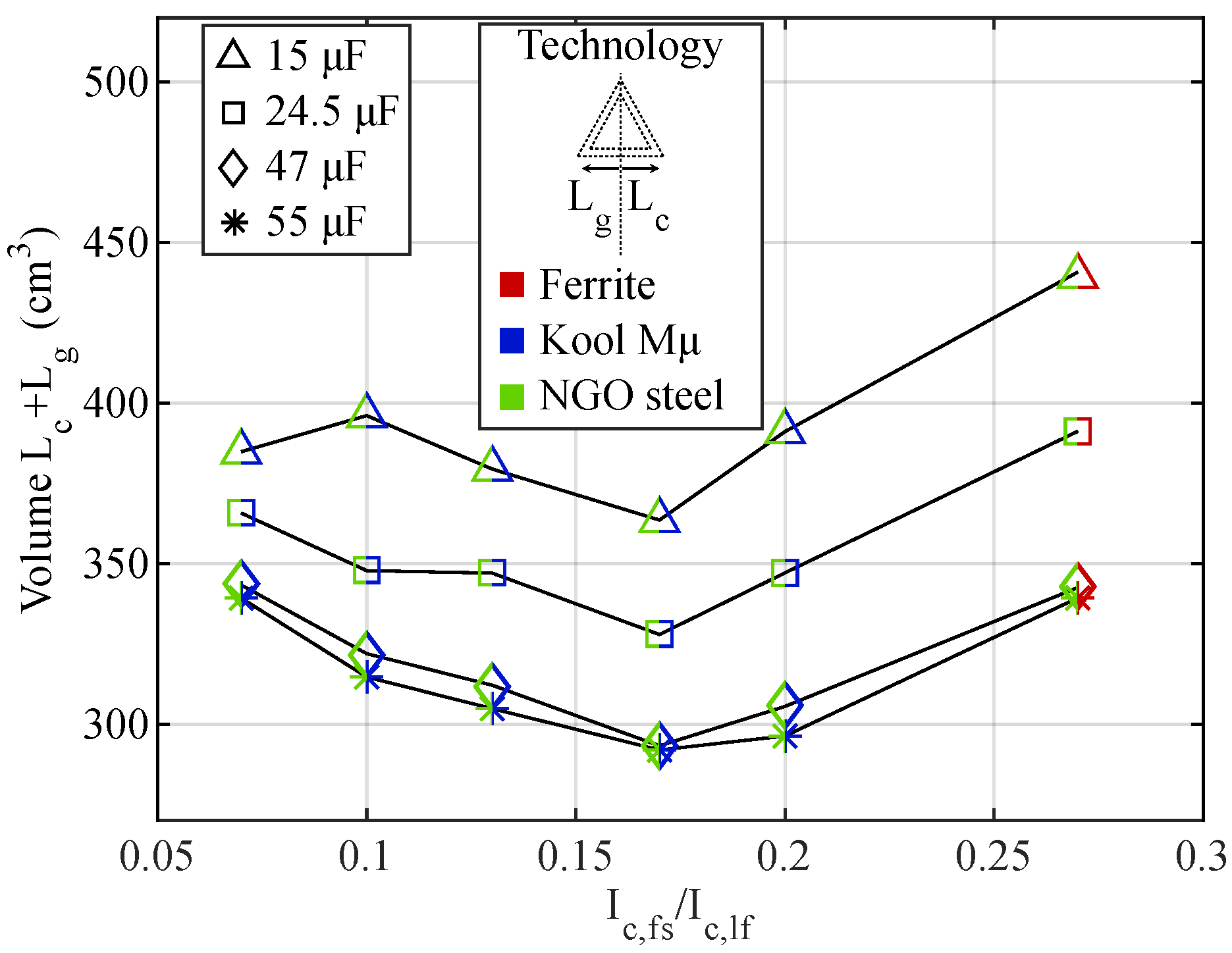
Based on the characteristics of each technology, the application of the proposed methodology makes it possible to select the magnetic material that will result in the smallest volume for and , for the considered values of and . The selection of the smallest volume for and for the converter from Table 1 will result in the volumes of shown in Figure 5. In it, the coloration of the markers identify which magnetic material resulted in the smallest volume for each inductor. The left side of the marker corresponds to the magnetic material of , and the right side to .
Having a freedom of choice for combinations of L-C-L considering normative restrictions, it is demonstrated that there is a specific value of that will result in the smallest inductor volumes.
4.2. Filter Capacitor
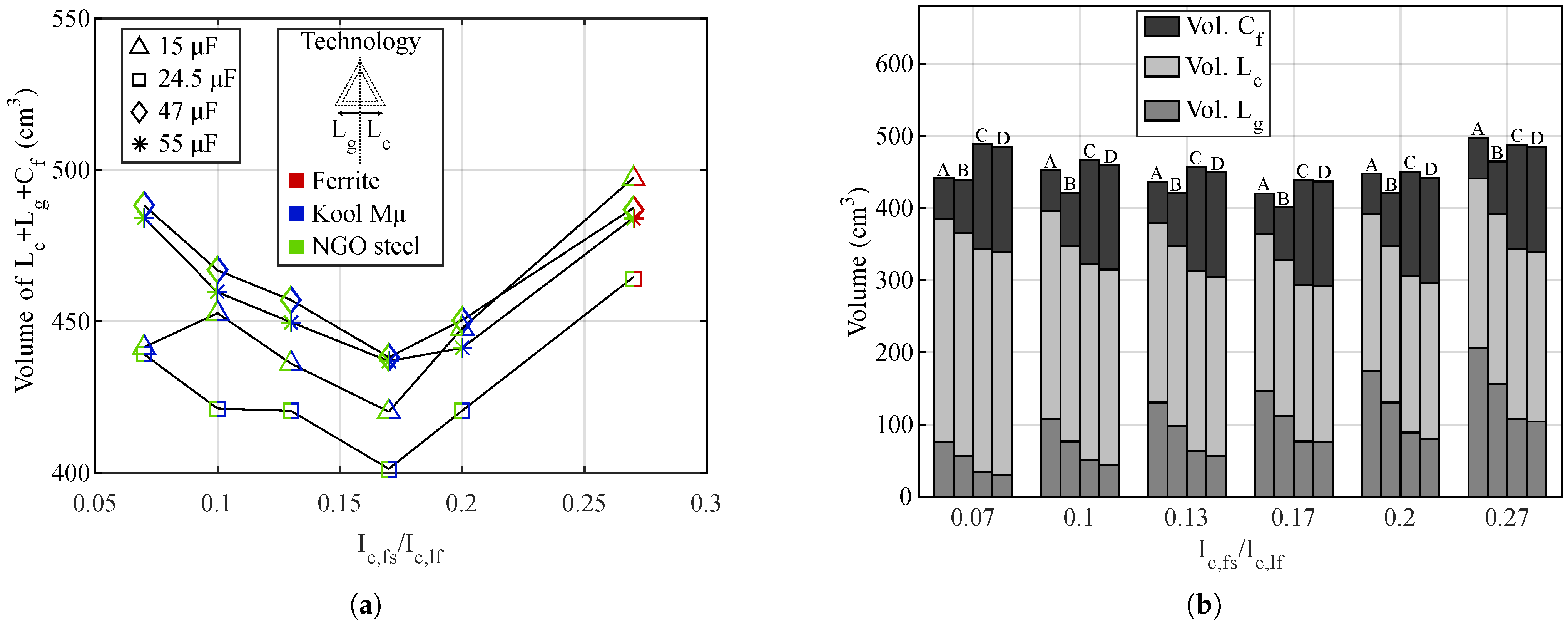
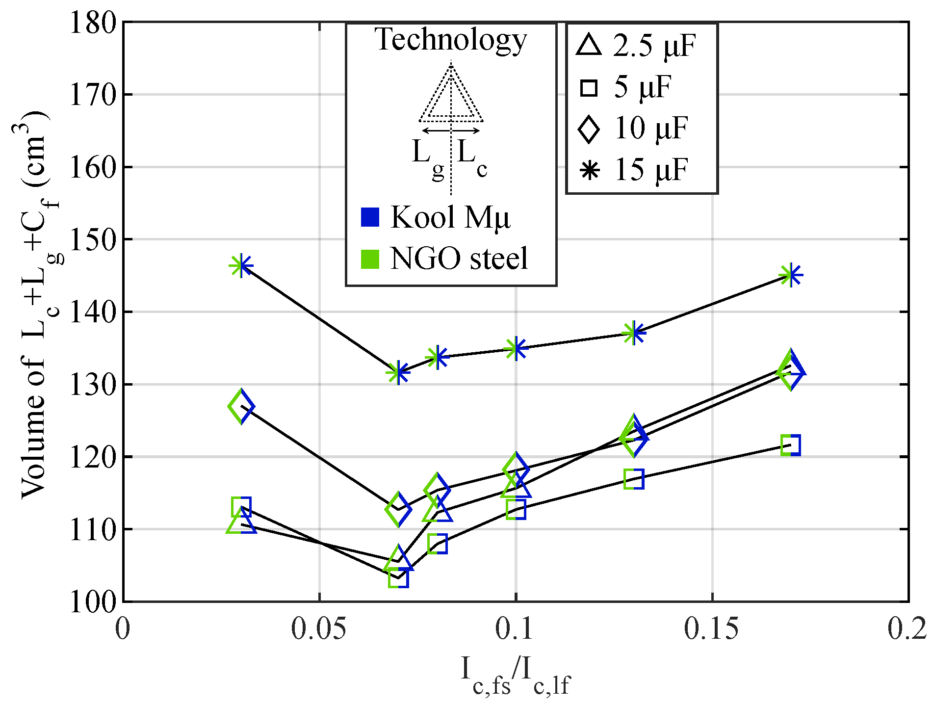
The complete analysis of the LCL filter volume is done considering the contribution of . Figure 6 shows the variation of the total volume () of the filter for the swept values of and . Similarly to Figure 5, the coloration of the markers identify which magnetic material resulted in the smallest volume for each inductor. The individual contribution of each component to the total filter volume is also shown. The combined volumes show that even if the largest capacitor values (47 µF and 55 µF) result in smallest inductor volumes (Figure 5), the intermediate value of 24.5 µF results in the smallest volume for the LCL filter (Figure 6).
The value of minimized filter volume, which corresponds to a I of approximately of the peak value of the sinusoid. The obtained value of differs from the recurrent decision to choose [1,8,15,37]. The capacitance value that minimized filter volume, µF, corresponds to 2.9% of , which is in accordance to the usual of [6,7,9,14,15,17].
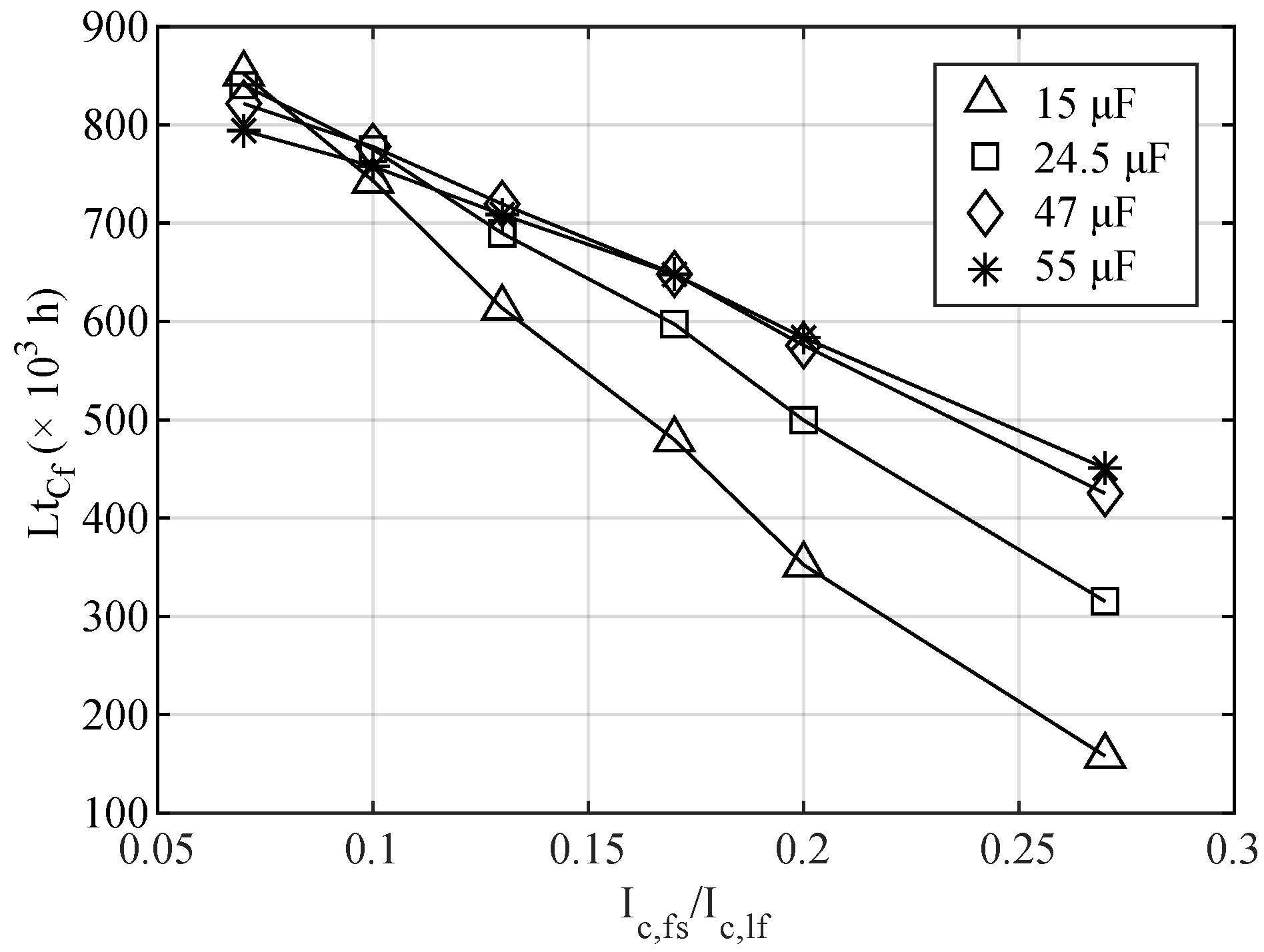
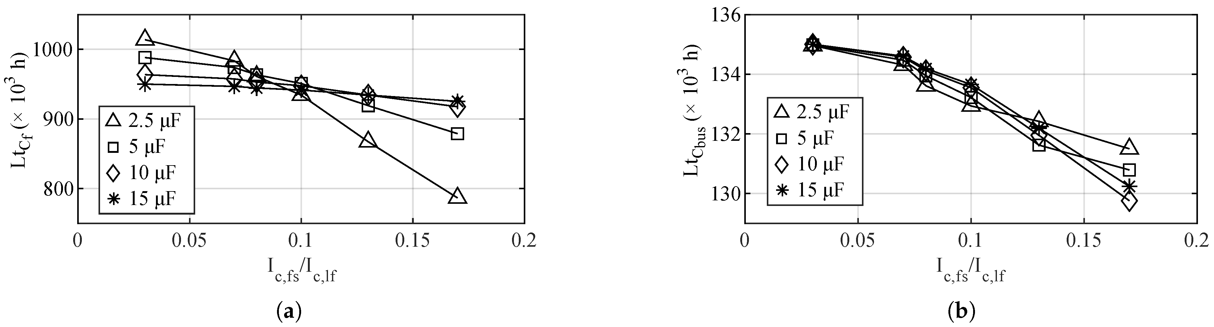
The second parameter under consideration for the LCL filter design is the filter capacitor lifetime. It is estimated using (9), resulting in Figure 7. For low , there is a longer estimated lifetime, due to the low harmonic content absorbed by the capacitor (at low most harmonics are filtered by ). As is increased, more harmonics are filtered by , increasing losses and reducing lifetime. Since and ESR are higher for the smaller capacitance values, the lifetime estimation for the 15 µF and 24.5 µF is significantly smaller than the others as is increased.
As can be seen in Figure 7, the highest estimated lifetime for all values of is given at the lowest value of (7%). If the value that minimizes filter volume (24.5 µF) is chosen for , the maximum design would result in an LCL filter with a volume 9.5% higher than the minimum volume, which was obtained at . In contrast, at the estimated lifetime is 29% smaller than at , choosing the latter could be considered a reasonable trade-off.
4.3. Bus Capacitors
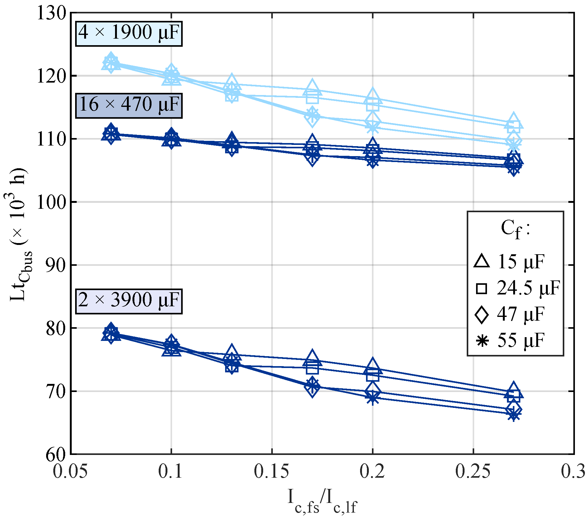
The last parameter under consideration is the bus capacitor lifetime. The total required capacitance () is calculated as a function of hold-up time [38]. The minimum capacitance of the DC Bus for the converter from Table 1 is estimated as mF. The following combinations of parallel capacitors were considered for each half of the DC bus: µF, µF, or µF. Their volumes are (each bus half): 632 cm, 352 cm, and 374 cm, respectively. The lifetime for each individual capacitor in the DC bus is estimated using (10), resulting in Figure 8. The variation of lifetime using the three possible combinations of parallel capacitors are plotted for comparison.
Given the tested configurations for the DC Bus, the overall best result in estimated lifetime was achieved using µF, besides having the smallest volume. This result may seem counter-intuitive, as it is expected that when the current stresses are divided among more capacitors (e.g., µF), estimated lifetime will increase. However, taking into consideration actual capacitor , ESR and current limits, when individual lifetimes are being considered, it is slightly worse to use 470 µF capacitors than using 1900 µF, for the DCMC series [36]. This seemingly counter-intuitive result demonstrates the importance of considering individual characteristics when designing the hardware, as was similarly shown in Section 4.1 for the inductors.
Similarly to , when increases, the estimated lifetime of decreases, because of the higher harmonic currents (Figure 8). is also influenced by , with higher values increasing harmonic currents in , reducing lifetime.
As discussed in Section 4.2, when using µF, the minimum volume for the LCL filter was obtained with , but the volume difference to (lowest value considered) was of 9.5%. Given the same capacitance value in the filter (24.5 µF), and with µF in the DC bus, the difference in between and is of 4.4%. This difference in lifetime is smaller than what was found for , which was of 29%. Since using benefits both and , the possible trade-off between filter volume and capacitor lifetime, mentioned at the end of Section 4.2, may continue be considered reasonable.
5. Experimental Results
The developed methodology for the LCL filter design is validated experimentally using two metrics. The first one is verifying that the designed filter meets the normative restrictions (IEC 61000-3-4), validating the parametric design (Section 2).
The second metric is the conformity of estimated power loss to the loss measurement, corresponding to the hardware design (Section 3). Capacitor lifetimes are directly related to their losses, as given by (7) through (10); and estimating inductor losses correctly is crucial for the entire design procedure, as described in Appendix A.
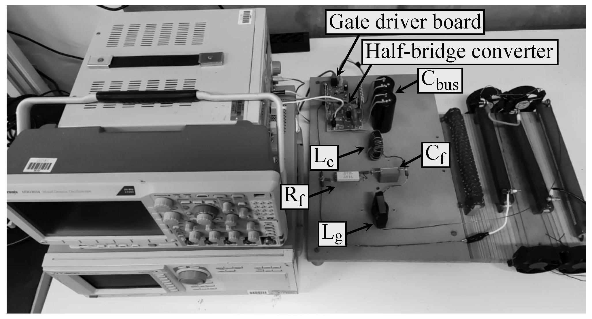
A 3 kW converter is considered as the case study for experimental results. To simplify the prototype, only a single-phase (1 kW) half-bridge is built, since the topology of Figure 2 allows that the LCL filter be designed per-phase. Furthermore, as described in Section 2, the LCL filter is designed to meet normative restrictions by itself, and therefore inductances of the grid and/or transformers at the input are disregarded. To avoid these influences, the converter is operated with reversed power flow, with a DC source at the bus, and a 1 kW load in series with (AC side). Either way, the LCL filter is attenuating the harmonics generated by converter switching.
The test setup is shown in Figure 9. Waveforms are measured with a Tektronix MDO3034 oscilloscope, and losses are measured using a Yokogawa WT1600 power meter. Total losses are . To separate semiconductor, filter, and DC Bus losses, the MOSFET losses () are estimated using the method presented by [39,40]. The estimated is equal to the sum of all estimated losses,
where and are the total losses (A15) estimated in the grid and converter-side inductors, and the losses (7) in the filter and bus capacitors, and joule losses in the damping resistor ().
The converter specifications for the experimental results (single-phase) are shown in Table 2. The methodology is applied considering a sweep of from 1.5% to 9.12% of , and from 3% to 17%. The resulting volumes are shown in Figure 10. The estimated lifetimes and are shown in Figure 11. Only one 1900 µF capacitor is used for each half of the DC bus.
The filter volume is minimized with µF and , as shows Figure 10. For these values, the lifetime of is only 1.5% smaller than the maximum value (at ), and for the lifetime is 0.3% smaller, as shows Figure 11. Though the capacitor lifetime is not maximized in this solution, it is considered a good compromise, and more useful than selecting , whose volume is 9.5% larger.
For the chosen operating point with µF, the corresponding inductances are µH and mH. The filter is designed to meet the IEC 61000-3-4 standard with a safety margin of 2/3 of the maximum admissible harmonic amplitude, or .
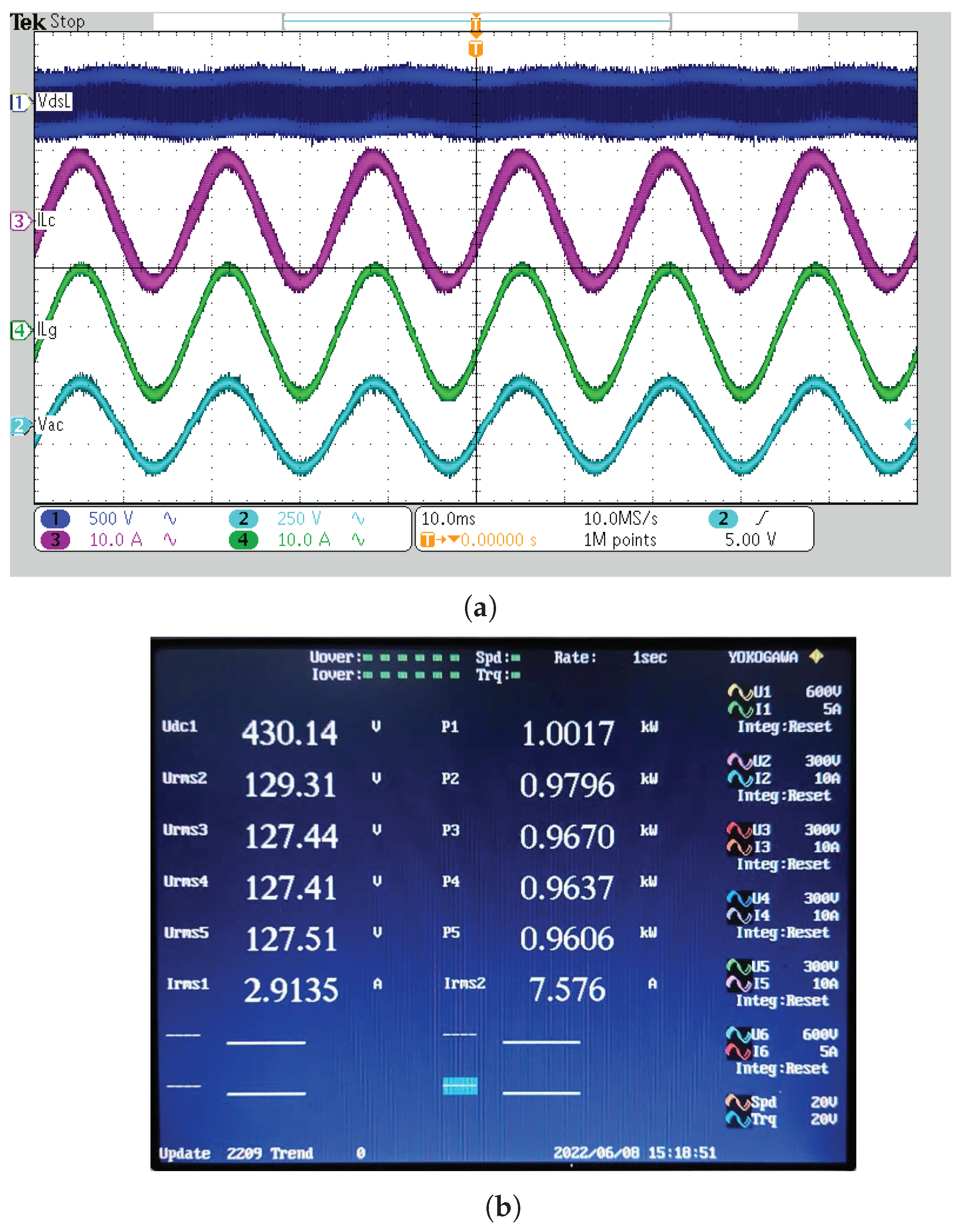
The oscilloscope and power meter measurements are shown in Figure 12. The oscilloscope waveforms in channel 1 show the drain-to-source voltage over the MOSFET; channel 2 the AC-side voltage; channel 3 the current in ; and channel 4 the current in . The total losses measurement is: W, corresponding to the reading of elements . Measurements were taken at other points of the circuit: W represents the losses of the converter (MOSFET and DC Bus combined); W represent ; W represent and combined; W represent . Estimated losses were: 3.66 W for ; 13.38 W for ; 0.10 W for ; 2.19 W for ; 16.49 W for ; and 3.50 W for , adding up to 39.32 W. The difference between the measured and estimated value is of 1.78 W, corresponding to 4.33% of the measured value.
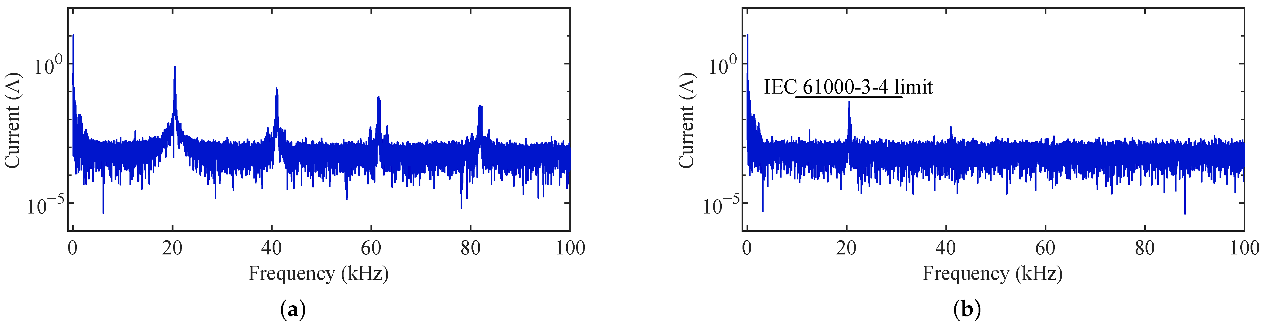
In Figure 13 the harmonic amplitudes of current over the frequency spectrum in and are presented. The measured ratio of is of 0.41%, close to the stipulated value of approximately 0.4%.
6. Conclusions
In this work a two-stage methodology for parametric and hardware design of LCL filters for grid-connected converters was presented. The first stage (parametric design) is based on the sweep of possible filter capacitances () and harmonic current content at the converter (). It is employed to determine different combinations of L-C-L that meet the restrictions of the standard. The second stage (filter hardware design) determines the hardware for each combination of L-C-L that was obtained in the first stage, taking into account practical aspects and particularities of each technology.
The influence of using different technologies for the core material of the inductors of the LCL filter was discussed. It was addressed how their individual characteristics relate to the frequency and switching harmonics, distinctly influencing the final design of each inductor. A step-by-step procedure for the parametric and hardware design of the components was presented. The relationship among the value of , the amount of harmonics absorbed by it, and how these influence the total volume of the LCL filter was also considered.
In addition to the filter volume criterion, the lifetime of the filter and bus capacitors was considered. In this way, a broader perspective design-wise was possible, where compromises between filter volume and capacitor lifetimes were discussed.
The results have shown that when using the proposed methodology, the joint analysis of the parametric and hardware designs makes it possible to identify the values of current harmonics and capacitances that minimize the filter volume, maximize the lifetimes of the capacitors, or a compromise between both, with all methods meeting the normative restrictions.
Author Contributions
Conceptualization, methodology, validation, writing—original draft, writing—review and editing: P.C.B., E.O.P., H.C.S., J.M.L. and J.R.P.; Supervision: P.C.B., H.C.S. and J.R.P.; Funding acquisition: H.C.S. and J.R.P. All authors have read and agreed to the published version of the manuscript.
Funding
This research was funded by the funding agencies CNPq (process 140848/2020-7) and CAPES (process 88887.597766/2021-00)—Financing code 001.
Institutional Review Board Statement
Not applicable.
Informed Consent Statement
Not applicable.
Data Availability Statement
Not applicable.
Conflicts of Interest
The authors declare no conflict of interest. The funders had no role in the design of the study; collection, analyses, or interpretation of data; in the writing of the manuscript, or in the decision to publish the result.
Nomenclature
The following nomenclature is used in this manuscript:
| A | Dowell’s equation term for winding geometry |
| area of the winding conductor | |
| core cross-section area | |
| core area product (window and cross-section area product) | |
| area occupied by the wire turns | |
| core window area | |
| maximum magnetic flux density attributed to the core | |
| high frequency peak magnetic flux density of the gth minor loop | |
| low frequency peak magnetic flux density | |
| base capacitance | |
| bus capacitor | |
| total bus capacitance | |
| lower-half bus capacitance | |
| upper-half bus capacitance | |
| LCL filter capacitance | |
| energy processing capability of an inductor | |
| equivalent series resistance of a capacitor at the ith frequency | |
| f | frequency for which the conductor is designed |
| fringing flux factor for a center gap | |
| fringing flux factor for a side gap | |
| low frequency (60 Hz) | |
| resonant frequency | |
| switching frequency | |
| G | number of high frequency loops present on a low frequency period |
| H | last harmonic multiple considered in the summation |
| h | harmonic multiple of the fundamental frequency |
| frequency domain amplitude of the converter-side inductor current | |
| root mean square value of a bus capacitor current | |
| root mean square current of the filter capacitor | |
| frequency domain amplitude of the converter-side inductor current at the | |
| switching frequency | |
| ratio between the switching frequency and low frequency amplitudes of the | |
| converter-side inductor currents in the frequency domain | |
| frequency domain amplitude of the capacitor current, at the ith frequency | |
| frequency domain amplitude of the converter-side inductor current at the | |
| fundamental frequency | |
| frequency domain amplitude of the grid-side inductor current | |
| frequency domain amplitude of the grid-side inductor current at the | |
| switching frequency | |
| ratio between the switching frequency and low frequency amplitudes of the | |
| grid-side inductor currents in the frequency domain | |
| frequency domain amplitude of the grid-side inductor current at the | |
| fundamental frequency | |
| peak current value of an inductor | |
| rated current of a bus capacitor | |
| root mean square value of the current flowing through the inductor | |
| J | current density |
| zero order Bessel function | |
| high frequency Steinmetz coefficient k | |
| low frequency Steinmetz coefficient k | |
| temperature coefficient | |
| core window utilization factor | |
| converter-side inductor | |
| length of the winding | |
| magnetic path length | |
| grid-side inductor | |
| gap length | |
| specified or required inductance (either grid-side or converter-side) | |
| estimated lifetime of an bus capacitor | |
| estimated lifetime of the filter capacitor | |
| rated lifetime of a bus capacitor | |
| rated lifetime of the filter capacitor | |
| modulation index | |
| N | number of turns |
| temperature stress coefficient of a bus capacitor | |
| voltage stress factor of a bus capacitor | |
| voltage stress coefficient of the filter capacitor | |
| number of winding layers | |
| number of parallel wire strands | |
| exponential temperature coefficient | |
| p | winding pitch, or spacing between conductors |
| capacitor losses | |
| total core losses | |
| total bus capacitor losses | |
| filter capacitor losses | |
| high frequency core losses | |
| low frequency core losses | |
| copper losses | |
| power measured at the input | |
| estimated losses at the converter-side inductor | |
| estimated losses at the grid-side inductor | |
| total measured power loss | |
| total inductor losses | |
| estimated MOSFET losses | |
| power measured at the output | |
| damping resistor losses | |
| core reluctance | |
| winding AC resistance | |
| damping resistance | |
| thermal resistance of the capacitor | |
| ambient temperature | |
| capacitor core temperature | |
| temperature of the filter capacitor | |
| inductor temperature | |
| temperature limit of a magnetic material | |
| rated temperature of a bus capacitor | |
| rated temperature of the filter capacitor | |
| frequency domain amplitude of the converter-side voltage | |
| time domain converter-side voltage | |
| voltage over a bus capacitor | |
| voltage over the filter capacitor | |
| frequency domain amplitude of the converter-side voltage at the switching frequency | |
| DC bus voltage | |
| core volume | |
| grid voltage (root mean square value) | |
| rated voltage of a bus capacitor | |
| rated voltage of the filter capacitor | |
| wire gauge to be used for stranding | |
| low frequency steinmetz coefficent | |
| high frequency steinmetz coefficent | |
| low frequency steinmetz coefficent | |
| high frequency steinmetz coefficent | |
| skin depth | |
| inductor temperature rise | |
| temperature difference between iterations | |
| temperature rise of a bus capacitor at | |
| magnetic permeability of the air | |
| relative magnetic permeability of the core | |
| copper resistivity |
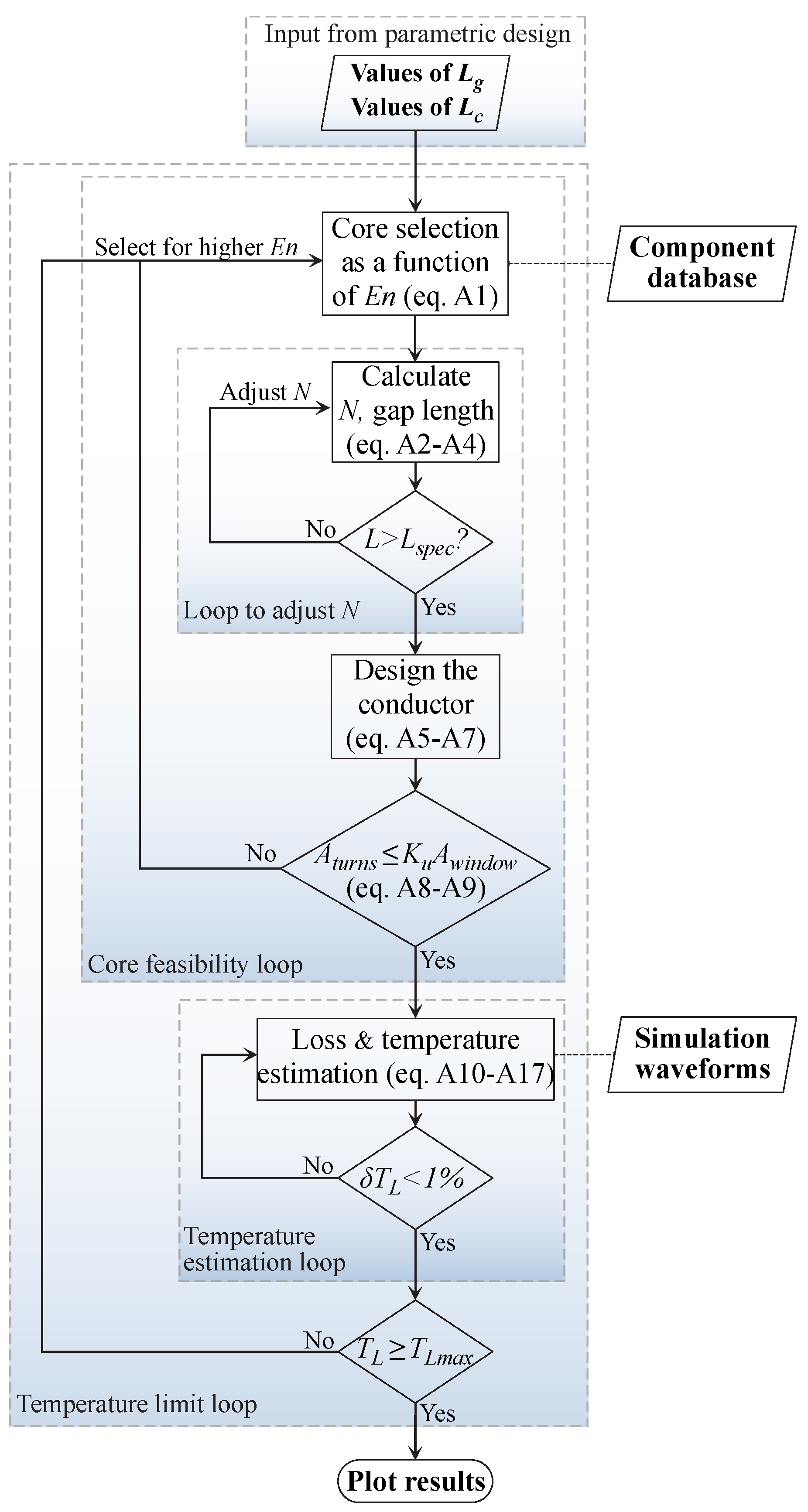
Appendix A. Inductor Hardware Design: Step-by-Step
A step-by-step procedure for the design of each inductor is presented in this section. The process is summarized in the flowchart of Figure A1. For each operating point obtained in the methodology presented in Section 2, and for each magnetic material, the inductor design begins by selecting a core from the database based on its energy processing capability (),
where is the specified inductance, either the value of or , determined with (3) or (4), and their respective peak current values. The right-hand side of (A1) is given by design constraints (, and J) and core dimension (): is the window area utilization factor; is core area product; is maximum magnetic flux density attributed to the core; and J the current density. For NGO steel material, the number of sheets is determined using the relation of to .
After the core is specified, the number of turns (N) are determined using core reluctance (),
at which is, for distributed gap (Kool Mµ) cores,
where is the magnetic path length; the core cross-section area; the magnetic permeability of the air; and the relative permeability of the core. For discrete gapped (ferrite and NGO) cores, is obtained by solving the magnetic circuit of an EI/EE core with three air gaps, that is, a core gapped at its center and side legs,
at which is the gap length; and the fringing flux factor for the side and center gaps, respectively [41]; and and the magnetic path length of the side and center legs of the core, which can usually be disregarded since is very high for gapped cores.
Exclusively for distributed gap (Kool Mµ) cores, due its gradual magnetic permeability loss characteristic, an inductance verification is performed to adjust the number of turns when necessary, in order to meet the specified inductance value (). This process forms a loop for the adjustment of N for distributed gap cores.
After determining N, the winding conductor area is determined based on J,
where is the RMS value of current going through the inductor. For , the wires are stranded, and therefore must be designed considering the skin depth (),
where is copper resistivity, and f the frequency for which the conductor is designed; in this case, the switching frequency. is used to select the commercial value of wire gauge () to be used for stranding, taking as the maximum radius of the strand. The number of parallel wire strands () is calculated based on ,
Next, an inductor construction (feasibility) check is done: the area for the wire turns () must be smaller than the available window area (),
If an inductor is not feasible, another core with higher energy is chosen from the database, and the design restarts, forming an inductor feasibility loop.
Figure A1.
Inductor hardware design flowchart.

Once the specified value for inductance () is met and constructive feasibility is confirmed, losses can be estimated using the component waveforms. Copper losses () are determined by the sum of the contribution of each individual current harmonic. Dowell’s equation is used to determine AC resistance () [42],
where represents the number of winding layers, the winding length, and A is a term given for a circular winding,
at witch p (pitch) is the spacing between the center of each conductor.
After determining the value of at each harmonic, is calculated as,
at which h represents the hth harmonic multiple of the fundamental frequency, and H the last harmonic multiple to be considered in the summation.
Core losses are calculated using Steinmetz equation, by separating hysteresis between the high frequency (HF) and low frequency (LF) loops, and summing the losses that result from each. The contribution to losses of the LF loop () is determined as,
at which , , and are the LF Steinmetz coefficients, the fundamental frequency (50 or 60 Hz), the LF peak value of magnetic flux density, and the core volume. On top of the fundamental LF waveform, there are HF minor loops present, with various values. To compute the contribution of the HF loops to core losses () their average value is used,
at which , , and are the HF Steinmetz coefficients, g identifies the gth minor HF loop, and the corresponding peak magnetic flux density of the gth loop.
Core losses () are computed by the combination of (A13) and (A14). Then, inductor total losses () are,
Temperature rise () on the inductor is estimated using (A16), which relates total losses to inductor surface area (),
at which and are the ambient and inductor temperatures, and and are empirical coefficients given for natural convection that relate inductor temperature in steady state to their total losses [41].
Since both and are temperature-dependent, they must be estimated iteratively. The first value used to determine losses is . After the first loss estimation, is calculated, resulting in a new value for . With it, losses are computed, and temperature rise is estimated once again. This process is repeated until the temperature rise between iterations () is smaller than 1%. If this condition is met, thermal equilibrium is assumed.
If the final is above the limit for a given magnetic material (), a larger (higher energy) core is selected from the database, and the whole design process is reset. Thus, an iterative loop is formed with the purpose of reducing inductor losses and .
The is particular to each magnetic material, and determined by the manufacturer. All magnetic cores were designed for a below 65% of their respective . This value, adopted as a safety margin, is a designer criteria, that can be easily changed in the proposed design methodology.
References
- Channegowda, P.; John, V. Filter optimization for grid interactive voltage source inverters. IEEE Trans. Ind. Electron. 2010, 57, 4106–4114. [Google Scholar] [CrossRef]
- Gurrola-Corral, C.; Segundo, J.; Esparza, M.; Cruz, R. Optimal LCL-filter design method for grid-connected renewable energy sources. Int. J. Electr. Power Energy Syst. 2020, 120, 105998. [Google Scholar] [CrossRef]
- IEEE Std 519-2014; IEEE Recommended Practice and Requirements for Harmonic Control in Electric Power Systems. IEEE: New York, NY, USA, 2014; pp. 1–29.
- IEEE 1547-2018; IEEE Standard for Interconnection and Interoperability of Distributed Energy Resources with Associated Electric Power Systems Interfaces. IEEE: New York, NY, USA, 2018.
- IEC TS 61000-3-4:1998; Electromagnetic Compatibility (EMC)—Part 3-4: Limits—Limitation of Emission of Harmonic Currents in Low-Voltage Power Supply Systems for Equipment with Rated Current Greater Than 16 A. IEC: Geneva, Switzerland, 1998; pp. 1–29.
- Reznik, A.; Simões, M.G.; Al-Durra, A.; Muyeen, S. LCL filter design and performance analysis for grid-interconnected systems. IEEE Trans. Ind. Appl. 2013, 50, 1225–1232. [Google Scholar] [CrossRef]
- Liserre, M.; Blaabjerg, F.; Hansen, S. Design and control of an LCL-filter-based three-phase active rectifier. IEEE Trans. Ind. Appl. 2005, 41, 1281–1291. [Google Scholar] [CrossRef]
- Pena-Alzola, R.; Liserre, M.; Blaabjerg, F.; Ordonez, M.; Yang, Y. LCL-filter design for robust active damping in grid-connected converters. IEEE Trans. Ind. Inform. 2014, 10, 2192–2203. [Google Scholar] [CrossRef] [Green Version]
- Sanatkar-Chayjani, M.; Monfared, M. Design of LCL and LLCL filters for single-phase grid connected converters. IET Power Electron. 2016, 9, 1971–1978. [Google Scholar] [CrossRef] [Green Version]
- Subroto, R.K.; Tsai, C.H.; Lian, K.L.; Karimi, H. Active Resonance Damping for an Ultra Weak Grid-Connected Voltage Source Inverter with LCL Filter based on an Optimization and Sliding Mode Control. In Proceedings of the 2022 IEEE/IAS 58th Industrial and Commercial Power Systems Technical Conference (I&CPS), Las Vegas, NV, USA, 2–5 May 2022; pp. 1–10. [Google Scholar]
- Zeng, G.; Rasmussen, T.W.; Teodorescu, R. A novel optimized LCL-filter designing method for grid connected converter. In Proceedings of the 2nd International Symposium on Power Electronics for Distributed Generation Systems, Hefei, China, 16–18 June 2010; pp. 802–805. [Google Scholar]
- Jalili, K.; Bernet, S. Design of LCL filters of active-front-end two-level voltage-source converters. IEEE Trans. Ind. Electron. 2009, 56, 1674–1689. [Google Scholar] [CrossRef]
- Said-Romdhane, M.B.; Naouar, M.W.; Belkhodja, I.S.; Monmasson, E. An improved LCL filter design in order to ensure stability without damping and despite large grid impedance variations. Energies 2017, 10, 336. [Google Scholar] [CrossRef] [Green Version]
- Ahn, H.M.; Oh, C.Y.; Sung, W.Y.; Ahn, J.H.; Lee, B.K. Analysis and design of LCL filter with passive damping circuits for three-phase grid-connected inverters. In Proceedings of the 2015 9th International Conference on Power Electronics and ECCE Asia (ICPE-ECCE Asia), Seoul, Korea, 1–5 June 2015; pp. 652–658. [Google Scholar]
- Lee, K.J.; Park, N.J.; Kim, R.Y.; Ha, D.H.; Hyun, D.S. Design of an LCL filter employing a symmetric geometry and its control in grid-connected inverter applications. In Proceedings of the 2008 IEEE Power Electronics Specialists Conference, Rhodes, Greece, 15–19 June 2008; pp. 963–966. [Google Scholar]
- Kang, H.H.; Jo, H.R.; Lee, K.B. Analysis of LCL-Filter Performance in Three-level Full SiC NPC Inverters with Inductor Core Materials. J. Electr. Eng. Technol. 2022, 2022, 1–8. [Google Scholar] [CrossRef]
- Sun, W.; Chen, Z.; Wu, X. Intelligent optimize design of LCL filter for three-phase voltage-source PWM rectifier. In Proceedings of the 2009 IEEE 6th International Power Electronics and Motion Control Conference, Wuhan, China, 17–20 May 2009; pp. 970–974. [Google Scholar]
- Muhlethaler, J.; Schweizer, M.; Blattmann, R.; Kolar, J.W.; Ecklebe, A. Optimal design of LCL harmonic filters for three-phase PFC rectifiers. IEEE Trans. Power Electron. 2012, 28, 3114–3125. [Google Scholar] [CrossRef]
- Liu, Y.; Lai, C.M. LCL filter design with EMI noise consideration for grid-connected inverter. Energies 2018, 11, 1646. [Google Scholar] [CrossRef] [Green Version]
- Zhou, D.; Song, Y.; Liu, Y.; Blaabjerg, F. Mission profile based reliability evaluation of capacitor banks in wind power converters. IEEE Trans. Power Electron. 2018, 34, 4665–4677. [Google Scholar] [CrossRef]
- Cupertino, A.F.; Lenz, J.M.; Brito, E.M.; Pereira, H.A.; Pinheiro, J.R.; Seleme, S.I., Jr. Impact of the mission profile length on lifetime prediction of PV inverters. Microelectron. Reliab. 2019, 100, 113427. [Google Scholar] [CrossRef]
- Wang, H.; Li, C.; Zhu, G.; Liu, Y.; Wang, H. Model-Based Design and Optimization of Hybrid DC-Link Capacitor Banks. IEEE Trans. Power Electron. 2020, 35, 8910–8925. [Google Scholar] [CrossRef]
- Busquets-Monge, S.; Crebier, J.C.; Ragon, S.; Hertz, E.; Boroyevich, D.; Gurdal, Z.; Arpilliere, M.; Lindner, D.K. Design of a boost power factor correction converter using optimization techniques. IEEE Trans. Power Electron. 2004, 19, 1388–1396. [Google Scholar] [CrossRef]
- Helali, H.; Bergogne, D.; Slama, J.B.H.; Morel, H.; Bevilacqua, P.; Allard, B.; Brevet, O. Power converter’s optimisation and design. Discrete cost function with genetic based algorithms. In Proceedings of the 2005 European Conference on Power Electronics and Applications, Dresden, Germany, 11–14 September 2005; p. 7. [Google Scholar]
- De León-Aldaco, S.E.; Calleja, H.; Aguayo Alquicira, J. Metaheuristic Optimization Methods Applied to Power Converters: A Review. IEEE Trans. Power Electron. 2015, 30, 6791–6803. [Google Scholar] [CrossRef]
- Jabr, R. Application of geometric programming to transformer design. IEEE Trans. Magn. 2005, 41, 4261–4269. [Google Scholar] [CrossRef]
- Dai, M.; Marwali, M.N.; Jung, J.W.; Keyhani, A. A Three-Phase Four-Wire Inverter Control Technique for a Single Distributed Generation Unit in Island Mode. IEEE Trans. Power Electron. 2008, 23, 322–331. [Google Scholar] [CrossRef]
- Wang, X.; Blaabjerg, F.; Loh, P.C. Grid-current-feedback active damping for LCL resonance in grid-connected voltage-source converters. IEEE Trans. Power Electron. 2015, 31, 213–223. [Google Scholar] [CrossRef] [Green Version]
- Parker, S.G.; McGrath, B.P.; Holmes, D.G. Regions of active damping control for LCL filters. IEEE Trans. Ind. Appl. 2013, 50, 424–432. [Google Scholar] [CrossRef]
- DI-MAX M-13 Non-Oriented Electrical Steel; AK Steel Corporation: West Chester, OH, USA, 2019.
- Iron Powder Catalog; Magnetics Inc.: Pittsburgh, PA, USA, 2020.
- Soft Ferrites and Accessories Data Handbook; Ferroxcube: San Diego, CA, USA, 2013.
- Ma, K.; Wang, H.; Blaabjerg, F. New approaches to reliability assessment: Using physics-of-failure for prediction and design in power electronics systems. IEEE Power Electron. Mag. 2016, 3, 28–41. [Google Scholar] [CrossRef]
- Wang, H.; Blaabjerg, F. Reliability of capacitors for DC-link applications in power electronic converters—An overview. IEEE Trans. Ind. Appl. 2014, 50, 3569–3578. [Google Scholar] [CrossRef] [Green Version]
- C4AF Printed Circuit Board Mount Power Film Capacitors; KEMET Electronics Corporation: New Taipei City, Taiwan, 2021.
- Type DCMC 85 °C High Capacitance, Screw Terminal, Aluminum; Cornell Dubilier—CDE: Liberty, SC, USA, 2021.
- Matsumori, H.; Shimizu, T.; Blaabjerg, F.; Wang, X.; Yang, D. Stability Influence of Filter Components Parasitic Resistance on LCL-Filtered Grid Converters. In Proceedings of the 2018 International Power Electronics Conference (IPEC-Niigata 2018-ECCE Asia), Niigata, Japan, 20–24 May 2018; pp. 3357–3362. [Google Scholar]
- Lai, Y.S.; Su, Z.J.; Chen, W.S. New hybrid control technique to improve light load efficiency while meeting the hold-up time requirement for two-stage server power. IEEE Trans. Power Electron. 2013, 29, 4763–4775. [Google Scholar] [CrossRef]
- Prado, E.O.; Bolsi, P.C.; Sartori, H.C.; Pinheiro, J.R. Simple analytical model for accurate switching loss calculation in power MOSFETs using non-linearities of Miller capacitance. IET Power Electron. 2022, 15, 594–604. [Google Scholar] [CrossRef]
- Graovac, D.; Purschel, M.; Kiep, A. MOSFET power losses calculation using the data-sheet parameters. Infineon Appl. Note 2006, 1, 1–23. [Google Scholar]
- McLyman, C.W.T. Transformer and Inductor Design Handbook; CRC Press: Boca Raton, FL, USA, 2014. [Google Scholar]
- Wojda, R.P.; Kazimierczuk, M.K. Winding resistance and power loss of inductors with litz and solid-round wires. IEEE Trans. Ind. Appl. 2018, 54, 3548–3557. [Google Scholar] [CrossRef]
Figure 1.
Diagram illustrating the developed methodology.

Figure 2.
Converter topology: input stage of double-conversion UPS with common neutral point connection.
Figure 2.
Converter topology: input stage of double-conversion UPS with common neutral point connection.

Figure 3.
Inductance of and as a function of , for different .

Figure 4.
Inductor volumes of and with different technologies as a function of , for different .

Figure 5.
Technologies that result in smallest combined volume of + , as a function of , for different .
Figure 5.
Technologies that result in smallest combined volume of + , as a function of , for different .

Figure 6.
Total filter volume: , as a function of , for different . (a) Results identifying inductor technology. (b) Individual component volumes, where each bar represents an analyzed value of , in ascending order: (A) 15 µF; (B) 24.5 µF; (C) 47 µF; (D) 55 µF.
Figure 6.
Total filter volume: , as a function of , for different . (a) Results identifying inductor technology. (b) Individual component volumes, where each bar represents an analyzed value of , in ascending order: (A) 15 µF; (B) 24.5 µF; (C) 47 µF; (D) 55 µF.

Figure 7.
Estimated lifetime for () as a function of .

Figure 8.
Estimated lifetime () for each capacitor in the DC bus, as a function of .

Figure 9.
Prototype for experimental results.

Figure 10.
Total filter volume: , as a function of , for the converter from Table 2.
Figure 10.
Total filter volume: , as a function of , for the converter from Table 2.

Figure 11.
Estimated capacitor lifetimes as a function of . (a) . (b) .

Figure 12.
Measurements. (a) Oscilloscope. (b) Power meter.

Figure 13.
Frequency domain amplitudes of inductor currents. (a) . (b) .


Table 1.
Converter specifications.
| Parameter | Value |
|---|---|
| Rated power | 15 kW |
| Switching frequency | 20 kHz |
| AC side voltage | 127 V/60 Hz |
| DC side voltage | 450 V |
Table 2.
Converter specifications for experimental results (single-phase).
| Parameter | Value |
|---|---|
| Rated power | 1 kW |
| Switching frequency | 20 kHz |
| AC side voltage | 127 V/60 Hz |
| DC side voltage | 430 V |
Publisher’s Note: MDPI stays neutral with regard to jurisdictional claims in published maps and institutional affiliations. |
© 2022 by the authors. Licensee MDPI, Basel, Switzerland. This article is an open access article distributed under the terms and conditions of the Creative Commons Attribution (CC BY) license (https://creativecommons.org/licenses/by/4.0/).
Share and Cite
MDPI and ACS Style
Bolsi, P.C.; Prado, E.O.; Sartori, H.C.; Lenz, J.M.; Pinheiro, J.R. LCL Filter Parameter and Hardware Design Methodology for Minimum Volume Considering Capacitor Lifetimes. Energies 2022, 15, 4420. https://doi.org/10.3390/en15124420
AMA Style
Bolsi PC, Prado EO, Sartori HC, Lenz JM, Pinheiro JR. LCL Filter Parameter and Hardware Design Methodology for Minimum Volume Considering Capacitor Lifetimes. Energies. 2022; 15(12):4420. https://doi.org/10.3390/en15124420
Chicago/Turabian StyleBolsi, Pedro C., Edemar O. Prado, Hamiltom C. Sartori, João Manuel Lenz, and José Renes Pinheiro. 2022. "LCL Filter Parameter and Hardware Design Methodology for Minimum Volume Considering Capacitor Lifetimes" Energies 15, no. 12: 4420. https://doi.org/10.3390/en15124420
Note that from the first issue of 2016, this journal uses article numbers instead of page numbers. See further details here.