
A Review of Nanomaterial Based Scintillators
by
 , and
, and
Sujung Min
1,2, 
Hara Kang
2,
Bumkyung Seo
2,
JaeHak Cheong
1,
Changhyun Roh
2,3,* and
and
Sangbum Hong
2,* 1
Department of Nuclear Engineering, Kyung-Hee University, Yongin-si 17104, Korea
2
Decommissioning Technology Research Division, Korea Atomic Energy Research Institute, Daejeon 34057, Korea
3
Quantum Energy Chemical Engineering, University of Science and Technology (UST), 217 Gajeong-ro, Daejeon 34113, Korea
*
Authors to whom correspondence should be addressed.
Energies 2021, 14(22), 7701; https://doi.org/10.3390/en14227701
Submission received: 25 October 2021
/
Revised: 10 November 2021
/
Accepted: 15 November 2021
/
Published: 17 November 2021
(This article belongs to the Special Issue Nuclear Engineering and Technology)
Abstract
:Recently, nanomaterial-based scintillators are newly emerging technologies for many research fields, including medical imaging, nuclear security, nuclear decommissioning, and astronomical applications, among others. To date, scintillators have played pivotal roles in the development of modern science and technology. Among them, plastic scintillators have a low atomic number and are mainly used for beta-ray measurements owing to their low density, but these types of scintillators can be manufactured not in large sizes but also in various forms with distinct properties and characteristics. However, the plastic scintillator is mainly composed of C, H, O and N, implying that the probability of a photoelectric effect is low. In a gamma-ray nuclide analysis, they are used for time-related measurements given their short luminescence decay times. Generally, inorganic scintillators have relatively good scintillation efficiency rates and resolutions. And there are thus widely used in gamma-ray spectroscopy. Therefore, developing a plastic scintillator with performance capabilities similar to those of an inorganic scintillator would mean that it could be used for detection and monitoring at radiological sites. Many studies have reported improved performance outcomes of plastic scintillators based on nanomaterials, exhibiting high-performance plastic scintillators or flexible film scintillators using graphene, perovskite, and 2D materials. Furthermore, numerous fabrication methods that improve the performance through the doping of nanomaterials on the surface have been introduced. Herein, we provide an in-depth review of the findings pertaining to nanomaterial-based scintillators to gain a better understanding of radiological detection technological applications.
1. Introduction
Nanotechnology is contributing to industrial development in a wide range of areas, including information and communication, biotechnology, medical care, the environment, energy, and sensors. Dr. Eric Drexler of MIT in the United States popularized the term ‘nanotechnology’ in the late 1980s [1]. He predicts that nanotechnology, capable of controlling materials on the nanometer scale, will change the world in the coming decades. In particular, it has been confirmed that the important concept in nanotechnology is not only size reductions but also the development of nanomaterials with unique shapes and structures. Nanotechnology has established a new technical field by connecting existing technical fields (e.g., physics, materials, and electronics). Nanomaterials are small, between 1 and 100 nm, and have excellent properties not observed in bulk forms. Size and shape control methods of nanoparticles are relatively simple. In addition, because they can be synthesized in an aqueous solution, there is an advantage in that a large number of materials can be synthesized relatively easily. Accordingly, various types of nanoparticles have been developed simultaneously [2,3]. The high ratio of the surface area to volume of nanoparticles increases the efficiency of catalysts and improves the sensitivity of sensors. In addition, particles synthesized with high purity levels have more advanced optical and electromagnetic properties, giving them many advantages in biological and clinical application research. As a result, the use of nano-biosensors has been expanded and now includes the detection of sensitive (or small amounts) cells in the human body and the ability to undertake precise examinations of local tissues in relation to medical diagnoses and clinical analyses. [4,5].
In general, particles used in high-sensitivity sensors include polymer nanoparticles, organic/carbon nanoparticles, biologically derived nanoparticles, and metal nanoparticles. Polymer-based nanoparticles are nano-sized solid particles that are synthesized by the polymerization of a monomer. Polymer nanoparticles may be less durable than metal nanoparticles, but they are widely used in medical fields because they can maintain strength levels similar to those of tissues and because they decompose in the body [6,7,8]. Metal nanoparticles have excellent durability and have unique physical, chemical, and electrochemical properties according to their size. In addition, there is the advantage of being able to amplify signals generated by fluorescent materials and low-molecular labeling materials based on the material properties of the corresponding metals. For example, the plasmon resonance phenomenon of metal nanoparticles can have the effect of amplifying certain optical properties, such as the Raman signal and fluorescent molecular signal. Surface-modified metal particles have excellent potential if applied to the development of sensor functions such as the amplification of electrochemical signals and improvements of sensitivity and selectivity capabilities. Therefore, this technology has been widely used in recent research related to sensors [9,10,11,12]. Organic/carbon nanoparticles exist in various structures and forms, such as single-walled carbon nanotubes (SWNT), multi-walled carbon nanotubes (MWNT), graphene, and carbon quantum dots. If carbon-based nanoparticles are applied to the sensor field, the resulting nanoparticles can offer many advantages due to their high surface-area-to-volume ratio, excellent electrical conductivity, good chemical durability, and high mechanical strength [13,14,15]. When a 3D material is nano-sized, it is referred to as a 0D material and is generally called a nanoparticle. A 1D material refers to a linear nanostructure having a lateral dimension of 100 nm or less. In addition, the 2D material has a layered structure similar to a thin sheet. 2D materials are characterized by a layered crystal structure with strong in-plane bonding, and the layers are bonded together by weak van der Waals (vdW) forces. Here, van der Waals force refers to the attraction between atoms, molecules, and surfaces. Van der Waals forces differ from covalent or ionic bonds because they are generated by polarization by nearby particles [16,17]. Unlike conventional quantum well semiconductors, control of the thicknesses of vdW semiconductors is done atomically. It is well known that device performance outcomes are degraded due to changes in the thickness of conventional semiconductor quantum wells [18]. 2D materials can be used in various ways because they have unique optical and electronic mechanical properties, and the atomic thickness and exposed surface can be designed and controlled, broadening the application range. Furthermore, in recent years, synthetic research on the stacking of 2D materials is being conducted. Research is focusing on 2D-0D, 2D-1D, 2D-2D, and 2D-3D structures given their superior performance to 2D materials for application to a wider variety of fields [19].
Recently, radiation detection sensors are being researched and developed for multiple sensors with small sizes, large areas, and good flexibility depending on the purpose. In particular, research on the development of sensors using nanomaterials as described above is being actively conducted worldwide. Research on and the development of radiation measurement and analysis technology has been steadily carried out in the nuclear field. And, as interest in radioactive waste and decommissioning has increased as an emerging issue. The development of radiation measurement sensors using nanomaterials has been carried out later than in other fields. When dismantling nuclear facilities, a large amount of radioactive waste is generated. Therefore, it is necessary to develop large measurement sensors because classification must be performed quickly after identifying the contamination level for radioactive waste. In addition, it is necessary to develop small sensors in multiple arrangements (e.g., Phoswich detectors) for radiation measurements and for continuous radiation monitoring in narrow places such as the pipes of nuclear facilities. With regard to decommissioning, high-purity semiconductor detectors (HPGe) or inorganic scintillators (NaI(Tl)) were widely used in the past, but these have disadvantages related to their size, complexity, and the need for expertise for these detectors. Plastic scintillators, which have many advantages in terms of utilization, show significantly lower detection performance capabilities than inorganic scintillators and semiconductor detectors. When a scintillator absorbs energy, electrons are excited and many electron-hole pairs are created. After a certain period (approximately 10−7s), the electrons deexcite and light is emitted. At this time, the emitted light is in the visible energy region, and the energy incident on the scintillator is analyzed through the emitted light. When nanomaterials are added to this scintillation mechanism, the optical performance is improved. In the nano-volume, there exhibit unique optoelectronic properties due to the quantum confinement effect of electron-hole pairs. In other words, when nanomaterials interact with incident radiation, the photoluminescence increases because not only energy transfers but also momentum transfers between them are induced by the quantum mechanical movement of electrons [9]. Using this principle, many studies have been conducted to develop functional nanomaterials with performance capabilities similar to those of semiconductor detectors or inorganic scintillators, with excellent process-ability and simplicity and that offer control of performance outcomes.
In this contribution, we review the present status of radiation detection and scintillator technology based on nanomaterials, including future prospects. In particular, the characteristics of organic as well as inorganic scintillators and nanomaterials are summarized and described in detail. In addition, functional materials for manufacturing high-performance scintillators and their fabrication methods are provided. Eventually, this review can serve as invaluable knowledge related to the development of nanomaterial-based scintillators.
2. Principle of Scintillators
Molecules are excited when charged particles and gamma rays react with materials such as NaI or ZnS. Materials such as NaI(Tl), ZnS(Ag), CsI(Tl) and CsI(Tl) are widely used as scintillators, most inorganic scintillators are made of alkali metal crystals and contain a small amount of impurities. A scintillator is a radiation detector that uses the luminescence phenomenon based on the excitation of radiation. The scintillator converts and amplifies the scintillation into a current pulse in a photomultiplier tube (PMT) and calculates the amount of incident radiation from the count value. Moreover, because the wave height of the obtained current pulse is proportional to the energy deposited by the incident radiation, the deposited energy can be calculated by analyzing the pulse wave height [20,21,22,23]. There is some luminescence of the scintillator, which is generated in the scintillation material due to the addition of an activator. Given that the various physical and chemical properties of the scintillator (density, atomic number, decay time, melting point, light yield, radiation length, refractive index, stability) are different for each scintillator, it is necessary to select an appropriate scintillator depending on the application. Scintillation occurs when a particle interacts with a crystal, and a device that measures and counts the scintillation is called a scintillation counter. The process of the reaction, amplification, and counting of the scintillation detector is shown in Figure 1 [24,25,26,27,28].
Scintillators have played a major role in the development of modern physics. The visual observation of scintillation on a zinc sulfide screen allowed Hans Geiger and Ernest Marsden to observe α particles, an event which can be considered as the starting point of modern nuclear physics. Up to the end of the Second World War, zinc sulfide and calcium tungstate were among the most popular particle detectors found in nuclear physics laboratories [6]. The intensive development of atomic projects in the postwar period stimulated the development of new ionizing radiation-detecting techniques, including scintillation counters. With the development of experimental physics and with the occurrence of the photoelectric multipliers, it became clear that scintillating materials are ideal devices to detect elementary particles and to measure their parameters [28,29]. In a fairly short time (1947~1951) it was discovered that scintillation can be observed in various organic and inorganic crystalline media [30,31,32,33], as well as in fluids [34,35,36,37], gases [38,39], and polymeric compounds [40]. At the same time, the most widely used scintillating crystalline material, NaI(Tl), was discovered [41]. Kallmann attempted to specify the essential parameters of scintillation materials [31]. He made a distinction between (a) the physical light output, which corresponds to the fraction of the absorbed ionizing radiation energy, which is transformed into light, and (b) the technical light output, which is the amount of light actually collected at the extremity of a scintillation element, taking into account all factors of light collection and absorption in the medium. In the Physical Encyclopedia, scintillation is defined as “short light flashes originating in a scintillator under the effect of ionizing radiation”. Fünfer and Neuert defined scintillation as “the phenomenon of luminescence in transparent solids, fluids or gases, originating at the propagation of the ionizing radiation through them” [24].
One may note that all of these definitions of scintillation have some shortcomings. First, while they are restricted to the phenomenology of light production under excitation by ionizing radiation, they do not consider the mechanism of energy transfer and conversion into light. From this point of view, Cherenkov radiators [42] could be considered as scintillators, which is fundamentally incorrect. A second limitation results from the confusion between scintillation and luminescence, which is at the origin of the semantic imprecision between scintillators and fluorescent materials.
There are three main forms of luminescence: fluorescence, phosphorescence and chemiluminescence. Fluorescence and phosphorescence are two forms of photoluminescence. Both fluorescence and phosphorescence are based on the ability of a material to absorb light and emit light of a longer wavelength and therefore lower energy level. The main difference is the time which it takes to do so. In fluorescence, the emission is basically immediate. A phosphorescent material can store the absorbed light energy for some time and release light later, resulting in an afterglow that persists after the light has been switched off. Depending on the material, this afterglow can last anywhere from a few seconds to hours. Incident photon and particles lose energy when traversing a medium according to the three fundamental mechanisms of electromagnetic interactions. The first is photo-absorption exhibiting a photoelectron effect and auger electrons (E < 30 keV). The second is Compton scattering, referring to interaction phenomena with the energy of incident photons (30 keV < E < 2 MeV). The third is the formation of an electron-positron pair (E > 2 MeV).
The interaction cross-section through each of these mechanisms is energy-dependent [43], photo-absorption and Compton scattering being dominant at low and medium energy levels and pair formation at high energy with an onset at 1.02 MeV, the mass energy of an electron-positron pair at rest. Neutral particles and charged hadrons lose energy mainly through direct interactions with nuclei or the ionization of atoms for charged particles. Knock-on electrons or γ or β decay from the relaxation of nuclei excited by neutron or neutrino capture will then lose energy through the standard electromagnetic interactions described above. If the energy of particles is high enough for multiple scattering and electron-positron pair creation, their energy is progressively distributed to a number of secondary particles of lower energy levels, forming an electromagnetic shower. Below the threshold of electron-positron pair creation, electrons will continue to lose energy through Compton scattering. For a material such as a crystal, another mechanism takes place at this stage. The electrons in the keV range from the shower will start to couple with the electrons and atoms of the lattice. They will excite the electrons from the occupied electronic states of the material (valence or deeper bound states) at different levels in the conduction band. At each of these interactions, an electron-hole pair is created. If the energy of the electron is high enough to reach the ionization threshold, we have then free carriers, which will move randomly in the crystal until they are trapped by a defect or recombine on a luminescent center. If the ionization threshold is not reached, the electrons and energy of the holes will cool due to coupling to the lattice vibration modes until they reach the top of the valence band for the hole and the bottom of the conduction band for the electron. They can also be bound and form an exciton whose energy level is in general slightly lower than the bandgap energy. At this stage, the probability is maximized for coupling to luminescent centers through either energy or a charge transfer mechanism. To make a scintillator, luminous centers must be included. Luminous centers are either extrinsic, general doping ions, or intrinsic, i.e., molecular systems of the lattice or of defects of the lattice which possess a radioactive transition between an excited and a lower energy state. Moreover, the energy levels involved in the radioactive transition must be contained in the forbidden energy band to avoid the reabsorption of the emitted light or photoionization of the center [44,45]. In a way, a scintillator can be therefore defined as a wavelength shifter. It converts the energy (or wavelength) of an incident particle or energetic photon (UV, X-ray, or gamma-ray) into a number of photons of much lower energy (or longer wavelength) in the visible or near-visible range, which can be easily detected with current photomultipliers, photodiodes, or avalanche photodiodes.
2.1. Inorganic Scintillators
The scintillation mechanism of the inorganic scintillator is determined by the structure of the crystal matrix. In a pure inorganic crystal matrix such as NaI, electrons can only exist within the energy band. However, electrons cannot exist in the forbidden band. When pure crystals absorb energy, electrons are excited from the valence band to the conduction band, and holes remain in the valence band. However, electron re-transition to the valence band with photon emission is an inefficient process. Photons emitted per incidence of decay are small, and the energy is emitted by other mechanisms. Additionally, the bandgap of pure crystals is large such that photons within the visible range cannot be emitted. Therefore, impurities in small amounts are added to scintillators. An inorganic scintillator is made of a crystal of an inorganic material containing a small amount of impurities (typically below a few percent), and this small amount of impurities becomes the emission point, referred to as an activator. Generally, inorganic scintillators are widely used for X-ray and gamma-ray measurements due to their large density levels and effective atomic numbers. For example, when a small amount of Tl is added to NaI, the bandgap (energy structure) in the matrix is deformed by Tl. As shown in Figure 2, an energy structure is generated in the activated parts of the scintillator, and an energy band is generated in the forbidden band in the pure crystal. Because the energy level generated by the activator in the crystal is smaller than the pure crystal, electrons can re-transit to the valence band. Emitted photons due to the transition of excited electrons have lower energy than emitted photons from pure crystals. That is, the emission spectrum is shifted to a longer wavelength and photons are emitted in the visible range. Charged particles (or photoelectrons) that pass through the crystal will create multiple electron-hole pairs. These holes quickly move to the position of the activator and the activation band is ionized. Because the ionization energy of the activation band is weaker than that of the normal matrix, the activation band is preferentially ionized and electrons excited with the activator rapidly transition within 10−7 s. As the atomic number increases, the binding energy approaches the photon energy. Therefore, the probability of photoelectric interaction is proportional to Z4–5 (Z is the atomic number). An inorganic scintillator is composed of a high-atomic-number material and has a high-density level, making the probability of photoelectric interaction high. In contrast, an organic scintillator is composed of a low-atomic-number material, meaning that the probability of photoelectric interaction is low. Figure 3 and Table 1 show the types and characteristics of inorganic scintillators. NaI(Tl) has high luminescence efficiency and high detection efficiency for gamma rays. However, in that it has deliquescent properties, it must be sealed and used in an Al container. Additionally, it is difficult in this case to measure alpha, beta, and low-energy X-rays, which have low permeability due to the Al container. CsI(Tl) has lower luminescence intensity and a lower energy resolution than NaI(Tl), but it has high mechanical strength [22,23].
2.2. Organic Scintillators
The organic scintillation mechanism differs from that of the inorganic scintillator. The energy of charged particles is absorbed and excites electrons in various states. The single state (spin = 0) is represented by S1, S2, and S3 in Figure 4, and for an organic scintillator, the interval between S0 and S1 is 3~4 eV. As the energy increases, the interval decreases. Each S level is subdivided into a series of levels with a finer structure (corresponding to the vibrational state of the molecule). Each typical S level is 0.15 eV [49,50].
The average energy at room temperature is approximately 0.025 eV, meaning that all molecules are in the S00 state. When charged particles pass through, the kinetic energy is absorbed into the molecule and electrons are excited. The higher energy states S2 and S3 quickly transition to the S1 state through an internal conversion mechanism. After excitation, the fluorescence intensity over time is calculated by I = I0e−t/τ. Here, τ is the fluorescence decay time at the S10 level. In most organic scintillators, τ is as short as the ns range. The life of the T1 state is much longer than that of the S1 state. The T1 → S0 transition causes phosphorescence (delayed luminescence). Because the T1 state is below S0, the wavelength of the emitted phosphorescence is longer than that of the fluorescence. Phosphorescence can be distinguished from scintillation based on the timing and wavelength. All fluorescence (except S10 → S00) has lower energy than the minimum energy required for absorption. There is little overlap between the emission spectrum and the absorption spectrum. Organic scintillators are not suitable for gamma-ray measurements, as they have a low probability of generating photoelectric effects because C, H, and O are the main components. Additionally, it is difficult to obtain large crystals and the mechanical strength is weak, making it difficult to be used in a crystal. Therefore, the scintillation material is used in the form of a liquid scintillator dissolved in an organic solvent or a polymerized plastic. The liquid scintillation material is very effective when used to measure nuclides that emit low-energy alpha and low-energy beta rays (H–3, C–14, etc.), as the detector can be manufactured in any size and shape and the measurement sample can be directly mixed with the scintillator [24,25].
3. Nanomaterials
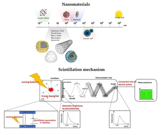
Nanomaterials in the 1~100 nm region (Figure 5) have unique properties that are not found in materials 100 nm or more in size. However, unlike conventional micron-sized materials that have certain properties useful in a wide range of fields, specific measurements and analyses are difficult in nano-sized materials because their properties vary greatly and change even with small changes in their size or composition near a specific size range [51]. Table 2 shows the characteristics of each nanomaterial [52,53,54,55,56,57,58,59].
3.1. Nanoparticle
Nano-sized materials have unique properties because they have a very large surface area compared to their volume. For example, one atom has a surface area of 100%. For nanomaterials with 3 × 3 × 3 atoms, the number of surface atoms among 27 atoms is 26. Similarly, nanomaterials consisting of 4 × 4 × 4 atoms have 56 of 64 atoms as surface atoms and 8 atoms as internal atoms. Thus, in the three cases above, the proportion of surface atoms among all atoms will gradually decrease from 100% to 96.3% and 87.5%. In other words, as the crystal size decreases, the ratio of surface atoms to all atoms increases significantly, causing a large change in the thermodynamic properties of the material. In general, because the surface atoms of solid material have greater free energy than the inner atoms, nanomaterials have much higher energy per unit atom than bulk materials. For a polycrystalline material made of nano-sized crystals, because the proportion of atoms belonging to the grain boundary has a relatively high open structure compared to a general polycrystalline material, the thermal expansion coefficient is very high, and the activation energy required for diffusion is reduced. Additionally, when the grain becomes fine in a polycrystalline material, there is a tendency for the strength and hardness to increase, whereas in a nano-crystalline material, the opposite tendency is also often observed. Nanomaterials are largely divided into zero-dimensional nanostructures, one-dimensional nanostructures and two-dimensional nanostructures (Figure 6) [60]. Quantum dots, which can be considered nano-sized dots, are classified as a zero-dimensional structure (Figure 6a), and one-dimensional nanostructures include nanorods, nanowires, nanotubes, nanocables, and nanobelts according to shape and size (Figure 6b). A typical thin film is classified as a two-dimensional structure Figure 6c). Table 3 shows the advantages and disadvantages of each type of nanomaterial [61].
3.2. Quantum Dots
The reason why nanomaterials are in the spotlight is that as the particle size decreases, they show different properties from the corresponding bulk particles and emit multiple colors depending on the size of the nanoparticle despite it being the same material as the bulk. New phenomena that occur as the material size decreases are often explained by an increase in the surface area, as shown in Figure 7. When a bulk material having a continuous energy state is thinly cut in one axial direction, it becomes a thin plate, and in this state, it takes on a staircase structure [62].
This is defined as a 2D quantum well state. If it is thinly cut again in another axial direction, the shape becomes a long line (rod) and the energy distribution becomes a discontinuous peak shape. This state is defined as a 1D quantum wire. When thinly cut in the remaining axial direction, it becomes a very small dot shape, and the energy becomes a 0D quantum dot state where only a specific position is allowed.
The effect of increasing the surface area as the size of the material decreases on the energy band is as follows. For example, considering the simplest case of a metal such as gold or silver, the densest method of gathering atoms on a two-dimensional plane is to surround one atom with six different atoms. Considering that they are stacked three-dimensionally, three different atoms are placed around the central atom on the lower and two-dimensional planes, resulting in the maximum stacking shape when a total of 12 atoms surround the central atom. This is defined as the hexagonal close-packed (HCP) or face-centered cubic (FCC) structure depending on the three atoms positioned at the top and on the bottom. All of the atoms in the interior form the most stable state by combining with the 12 surrounding atoms, but the atoms on the surface are in a relatively unstable state due to the absence of the 12 surrounding atoms. Therefore, the energy state of these surface atoms differs from that of the atoms inside. When starting from the central atom and surrounding it with other atoms in the form of a shell to increase its size, geometrically the number of atoms in each shell is (10n2 + 2). As the size increases, the total number of atoms increases to 1 → 13 → 55 → 147 → …, and the number of surface atoms increases to 1 → 12 → 42 → 92 → …, with the proportion of surface atoms among all atoms being 92; this will gradually decrease from 92% → 76% → 63% → …, Normally, nanoparticles are made up of tens to thousands of atoms, and the proportion of atoms on the surface is approximately 10% to 50%. In the bulk, the proportion of atoms on the surface is negligibly small such that the effect of these elements is ignored and expressed only by the properties of the atoms inside. However, if the proportion of surface atoms increases, the properties of the surface atoms according to the energy state can no longer be ignored, and small bands in a new state are additionally generated at both ends of the energy band of the material. Due to these new energy states, nanomaterials have electrical, optical, and magnetic properties that are completely different from those of the corresponding bulk materials, and their reactivity is greatly changed. Particularly in the case of semiconductor materials, due to newly generated small energy bands, the bandgap energy value inherent to the semiconductor material changes with the size, and a new phenomenon in which a color known as a material’s unique physical property changes with the size occurs. The quantum dot is one such artificially synthesized nanostructure, and it typically refers to a micro-cavity capable of containing electrons defined in a semiconductor material having a size within 100 nm. Just as electrons are constrained by the potential energy of the atomic nucleus, quantum dots are also called artificial atoms because electrons are constrained by an artificially applied potential such as an external voltage [63,64].
Quantum dots can be viewed as solid crystals in which quantum confinement occurs in all three-dimensional directions. There are many types of quantum dots, such as CdS, CdSe, PbS, and InP, and different colors are emitted when light of different wavelengths is emitted depending on the size of the quantum dots. For example, as the size of the CdS quantum dot decreases, the color shows a blue shift from red to blue. It is easy to understand how quantum dots interact with light by looking at the quantum binding effect.
In quantum mechanics, light consists of photons with energy hc/λph. (For reference, a red photon has about 1.8 eV of energy, the green photon about 2.5 eV, and the blue photon has energy of about 3.2 eV.) The energy of a photon with a wavelength of λph has the energy of a quantum dot. When it becomes equal to the energy difference between the levels, that is, when (En+1 − En) = hc/λph, light of a corresponding wavelength is absorbed. In addition, when the quantum dot transitions from a state having energy En+1 to a state having energy En, light with the wavelength corresponding to the above equation is emitted. The smaller the size of the quantum dot is, the greater the energy difference between energy levels in the quantum dot becomes. Therefore, as the size of the quantum dot decreases, the energy of light interacting with the quantum dot increases. This phenomenon is defined as a “blue shift” [53,64].
3.3. Perovskite
The crystal of a mineral is made up of repeating arranged atoms with regular rules, and the regular arrangement of these atoms is called a crystal matrix. The crystal matrix is a form in which the simplest basic unit, called a unit matrix or unit cell, is repeatedly stacked. Perovskite is a substance having the general formula of AMX3, and two types of cations (A, M) and one type of anion (X) are combined to form a three-dimensional crystal, as shown in Figure 8. The A atom is located at each vertex of the cubic unit matrix, the M atom is located at the body-center position, and the X atom is at the face-center position [65].
Inorganic perovskites, such as BaTiO3, KbTiO3, and PbTiO3, in which both types of cations are made of metal, are generally known, and the forms of oxygen in the place of the anion(X) have mainly been studied. Recently, organic-inorganic hybrid perovskites, perovskites containing inorganic and organic substances on the cation site and halogenates on the anion site, have attracted considerable attention as they have the advantages of both inorganic and organic materials. When an organic substance enters, its characteristics are such that the conductivity of the substance can be controlled by changing the organic substance chain. CH3NH3PbI3, in which Cs is replaced with methylammonium in the existing inorganic perovskite CsPbX3, is a typical material used in high-performance perovskite solar cells. The perovskite has another characteristic when it forms nanocrystals. If the crystal structure is not of a size commonly known in everyday life but a billionth of this size, i.e., on the nanometer scale, it will show interesting properties. Perovskite nanocrystals, now known in the nanotechnology world, have a new property called ‘charge amplification’. Normally, in a solar cell, when a semiconductor converts light energy into electricity, it carries a current by generating a single free electron, a hole. However, in a perovskite material, if there is sufficient light energy, more than one electron-hole pair is formed, and conversion to electricity can be achieved. This can be explained by the phenomenon of local surface plasmon resonance. When a nanometer-sized metal absorbs light of a specific wavelength, free electrons on the surface collectively vibrate strongly and the electron flow is greatly amplified. Because perovskites are made of ionic crystals, they have the advantage of easy adjustment of the balance characteristics affecting high mobility and recombination of electrons and electrons. In addition, they can be synthesized from materials of any other composition and are easily manufactured into quantum dots or nanocrystals. In addition, they have high flexibility and can be made thin. Perovskites are typically used in solar cells and light-emitting diodes (LEDs). Solar cells are an example of using light absorption among the characteristics of a perovskite. Perovskites have high photoelectric efficiency. Photoelectric efficiency refers to efficiency when converting the movement of light, that is, photons, into electricity, and is used in solar cells with these characteristics. The organic-inorganic hybrid structure of perovskites shines in solar cells. Because organic-inorganic hybrid perovskites are used as a photoactive layer, they are lighter and more flexible than an inorganic material alone and have superior charge transfer ability, accumulating both electrons and holes compared to organic dyes, which do not have charge transfer abilities. This offers the advantage of increasing the life of the electron-hole pair. In addition, high temperatures of more than 1000 °C are required, and economic value can be realized because they are produced through an inexpensive solution process, unlike a silicon solar cell and its complicated process. Other advantages are low economic value and few restrictions on the installation locations and application fields.
LEDs are examples of the use of perovskite light emission. A light-emitting diode is a semiconductor device that emits light when current flows through it and electrons and holes recombine, converting and emitting electrical energy into light energy. Therefore, the luminous efficiency increases as the combination of electrons and holes in the semiconductor become better. This is the conversion of energy in the opposite direction of the solar cell. Perovskites are attracting attention as a new LED material and have the advantages of a simple manufacturing process and superior color purity while having the impossible price of one-tenth of that of existing OLEDs (organic light-emitting diodes) in terms of materials. Perovskite nanoparticles have different colors depending on the type of halogen element (X) inside. If the level of iodine (I) is high, red is emitted; high bromine (Br) levels produce green, and high chlorine (Cl) levels are associated with blue light [65,66].
Figure 8.
Structure of Perovskite [67].
Figure 8.
Structure of Perovskite [67].

3.4. 2D Materials
3.4.1. Graphene
2D materials have a planar structure. For example, graphene is a typical 2D planar material with a hexagonal honeycomb structure composed of only carbon. Graphite is also a carbon-only material. Graphite has the property of being easily separated because it is covalently bonded in the same layer with weak bonds called van der Waals bonds between the layers. If graphite of this structure is continuously separated between layers, a single layer of graphene can be obtained. Graphene has a relatively high absorption of light, but it is very thin, meaning that it is also transparent and flexible, with good electrical properties. In addition, mobility, which is one of the characteristics of semiconductors, has a very high value of close to 200,000 cm2/V∙s and its conductivity is also good. In general semiconductors, the valence band and conduction band are separated by a bandgap. However, as shown in Figure 9 graphene has a structure in which two bands are in contact with each other at one point in the momentum space. This band structure has all the advantages and disadvantages of the electrical properties of graphene. The advantages of conductivity and high mobility are due to the metallic nature of graphene. The disadvantage is that there is no difference between the on-state current and the off-state current due to the absence of the bandgap. For a good semiconductor, the on-state current and the off-state current differ by approximately 108, whereas for graphene the difference is only approximately 10 to 100 times. With these characteristics, it is difficult to use graphene as a semiconductor. However, many studies have been conducted to overcome these shortcomings and to devise methods by which to remove the symmetry of graphene. A typical method is to stack graphene nanoribbons and graphene in two layers. First, graphene in the form of nanoribbons loses its one way symmetry, creating a bandgap through the creation of numerous edge effects. When the nanoribbon thickens, the bandgap becomes zero, and when the width is narrower, a bandgap arises. However, it is very difficult to create a 1 nm nanoribbon, and the bandgap is only 1eV. Additionally, the mobility of transistors is poor. A second method is to stack graphene in two layers. This method also has shortcomings similar to those of nanoribbons. As shown in Figure 9, a bandgap arises when an electric field is loaded on an energy band split by the interaction between the two layers [68,69,70,71,72,73,74].
The schematic band structure of pristine graphene with the linear energy-momentum dispersion relationship of E = hv|K| is shown in Figure 9a. The valence and conduction bands are conical and meet at point K (Figure 9b). Figure 9c,d show the schematic band structures of p-type and n-type graphene with the bandgap and Fermi level (Ef) in the valence and conduction bands, respectively.
3.4.2. Carbon Nanotube (CNT)
First discovered in 1991 by Dr. Sumio Iijima of Japan, a carbon nanotube is a spiral material in which six hexagonal carbon atoms are connected in a tube shape to form a net structure [75]. Depending on the angle and direction of the material, it can become an electrical conductor or a semiconductor. In particular, the diameter is about one-hundredth of the thickness of a human hair, which is very fine, but its strength is nearly 100 times that of steel. In addition, it has high thermal conductivity and electrical conductivity, boasting a wide range of uses above those of ordinary carbon fiber. Therefore, carbon nanotubes are in the spotlight in such areas as aircraft, automobiles, secondary batteries, and semiconductors, where electricity and heat conductivity and strength of the material are important. In the future, it is expected that more convenient production methods will be developed and activated in various industries and with a range of technologies [76,77,78,79,80,81,82,83].
4. Synthesis and Fabrication of Nanomaterials
In Table 4 and Table 5, various nanoparticle synthesis methods are known, which can also be applied to semiconductor quantum dot synthesis. Nanoparticle synthesis methods can be largely classified as top-down synthesis methods and bottom-up synthesis methods. First, the top-down synthesis method is a destructive approach, starting with larger units and breaking them down into smaller units to synthesize nanoparticles. Examples of this method include grinding/milling, CVD, and PVD (physical vapor deposition) methods. In earlier research, under the presence of an organic oleic acid, a top-down destruction approach was used to synthesize spherical magnetic light nanoparticles with a particle size of 20 to 50 nm from natural iron oxide (Fe2O3) ore. In addition, in 2004, colloidal carbon spherical particles that could be controlled by simple top-down methods were synthesized. The bottom-up synthesis method is an example of the reverse utilization of the top-down synthesis method, with a precipitation and reduction technique. Recently, LDL nanoparticles were synthesized without a phospholipid via a solvent-exchange method, and single-variance spherical bismuth (Bi) nanoparticles were synthesized using both methods [84]. The most commonly used classical methods, bottom-up and top-down methods, refer to the reduction of metal acids or metal salts in a solution; a typical example is the synthesis of gold nanoparticles using a chloroauric acid solution. When gold ions are reduced using sodium citric acid (sodium citrate), the reduced gold atoms gather to form gold nanoparticles. Later, when the surface of the gold nanoparticles is covered with protective substances, clumping is prevented. The size of the nanoparticles formed is adjusted according to the pH of the initial solution, the concentration of the reducing agent, and the temperature. Semiconductor nanoparticles such as CdS or CdSe may be synthesized using a colloidal chemical methodology called the inverse micelle process. The reverse micelle method has the advantage of being able to cover the surface of already formed nanoparticles with additional chemical reactions. There is also a method of synthesizing various types of semiconductor nanoparticles after putting metal salts and chalcogenide reactants in zeolite and Nafion polymer film. However, this method does not determine the physical size of the nanoparticles in which a material hole is formed, unlike the reverse micelle method, and the difference is that the formed nanoparticles are permanently embedded in the zeolite or Nafion polymer matrix. Studies are being actively carried out at home and abroad to make high-quality semiconductor nanoparticles, where ‘high-quality’ means that the nanoparticles have excellent crystallinity, high luminance, and small size distribution. These high-quality semiconductor nanoparticles are divided into different nanocrystal types [85,86,87,88,89,90].
5. Nanomaterial-Based Scintillators
In nanomaterials, the control of electron-hole pairs and the efficient generation of multiple excitons, that is, the generation of multiple electron-hole pairs by one photon, are unique photophysical properties of nanomaterials. In bulk scintillators (Figure 10a), electron-hole pairs lose their energy while emitting phonons and are located at the edge of the band. On the other hand, in nanomaterials (Figure 10b), the quantized energy level creates a phonon bottleneck, which can transfer energy to the creation of new electron-hole pairs instead of phonon emission [91]. Therefore, unlike the bulk scintillator, the nanomaterial-based scintillator can improve the efficiency as well as control the emission wavelength according to the type and size of the nanomaterial used. In addition, there is an advantage that the reaction rate with photons can be improved by using nanomaterials with high atomic numbers. However, nanomaterials tend to aggregate because of their large specific surface area. Therefore, it is important to uniformly disperse the nanoparticles when depositing them on a polymer.
A reaction in which two or more molecules combine to form a compound with a high molecular weight is called polymerization. A thermal polymerization method is generally used when manufacturing a scintillator, and there is a polymerization method using light, radiation, or a catalyst. Table 6 describes the nanomaterial doping and scintilaltor fabrication methods used in the research cases mentioned in this review.
The study of quantum dot synthesis methods was accelerated after the Bowendi group at MIT in the 1990s when they reported a quantum dot synthesis method of the high-quantum-efficiency cadmium series. Various quantum dots have been reported thus far, including the cadmium series, II–VI, III–V, IV–VI, and I–III–V. The properties of quantum dots also change depending on the material, and quantum dots, commonly called cores, do not have good luminous properties. However, there are reports of ways to maximize these characteristics by wrapping them with a shell structure or creating them in an alloy form. These methods can simultaneously increase the efficiency and stability of quantum dots.
In 2018, Chen Q. et al. [92] conducted a study using perovskite nanocrystals. In a typical bulk scintillator material, it interacts with high-atomic-number materials to generate many photoelectrons through photoelectric effects. It is possible to control the color of perovskite quantum dots by controlling the emission wavelength, resulting in a narrow half-peak emission peak. However, the emission spectrum of the bulk scintillator is uncontrollable and shows an emission peak with a large half width. In that study, these properties of perovskite ionization crystals were utilized to develop a prototype device for multi-colored X-ray detection through a combination of solution processing and soft lithography, with a subsequent comparison with commercial bulk scintillators (CsI:Tl, PbWO4, YAlO3:Ce and Bi4Ge3O12). After analyzing the X-ray absorption spectrum of carbon, CdTe, and CsPbBr3, the authors of the paper [92] found that Pb-based perovskite nanocrystals are more suitable for photon detection scintillators than nanocrystals without Pb components. In addition, the authors observed that the bandgap energy of perovskite nanocrystals is in the range of 1.7~3 eV and that the energy density reaches its maximum when the atomic distance is 10.32 Å. The prototype device developed in the study was manufactured by spin-coating a perovskite material, and it was confirmed that the lowest detection dose rate was 13 nGy/s. This value is approximately 420 times lower than the dose (5.5 uGy/s) used for a general X-ray diagnosis. In addition, it was confirmed that a very rapid response (τ = 44.6 ns) was obtained from the Cs-137 source. Rapid responses to X-rays are crucial important factors in medical radiography. In addition, the characteristics of the perovskite and commercial bulk scintillators (CsI; Tl, PbWO4, YAlO3; Ce and Bi4Ge3O12) were compared. The perovskite showed good luminescence sensitivity to X-rays, with multi-color high-efficiency luminescence found to be possible. On the other hand, conventional scintillators have poor resolutions of the emission peaks. Therefore, it is difficult to express multi-color visualization by photons. In the aforementioned study, it was confirmed that perovskite nanocrystals showed a very rapid response (44.6 ns) to X-rays, and the scintillator using the perovskite can be converted into multi-colored visible light, which has a small half width. It was also confirmed that use as a scintillator was possible. The results of the study appear to be applicable to the X-ray sensing and the imaging industry, with perovskite materials also useful as alternative materials in solar and light-emitting diode applications.
In 2019, Chang S. et al. [93] conducted a study to improve the luminescence using quantum dots and developed a method of uniformly doping quantum dots covered a thiol. Here, the thiol is an organic sulfur compound (R-SH) structure, R is an alkyl or other organic substituent, and -SH denotes a sulfhydryl group (sulfhydryl group). The thiol (R-SH) binds to the quantum dot and protects the surface of the quantum dot. Samples were prepared using three types of quantum dots (MPA-CdTe, MPA-CdSe, and Cys-CdTe) and the properties were evaluated. MPA is mercaptopropionic acid, and Cys stands for cysteamine. As a result of evaluating the characteristics of quantum dots using the emission spectra, TEM, and XRD patterns, it was confirmed that the type and particle sizes of quantum dots influence their luminescence and quantum efficiency. These results are confirmed in Figure 11 and Figure 12 in that study, three types of quantum dots were synthesized, and the synthesized quantum dots were enhanced by a chemical reaction with photons by a high-energy gamma irradiation method in an aqueous solution. Photons can interact with water molecules, organic ligands (MPA or Cys) and inorganic nanocrystals (CdTe or CdSe). Water molecules are decomposed by photons to generate active species such as H−, HO−, HO2−, and they interact with nanocrystals such as CdTe or CdSe to release Cd2+ ions. S2− and Cd2+ can also be generated by direct interaction between photons and quantum dots. The resulting S2− and Cd2+ combine rapidly to form CdS, with the photons releasing S2− and Cd2+ very slowly such that a CdS shell is formed on the quantum dot surface rather than the on CdS particles in the solution. Thus, a thin CdS shell can reduce defects on the CdTe or CdSe quantum dot surfaces. Because the bandgap of CdS is wider than those of CdTe and CdSe, the formation of a thin CdS shell is considered a key factor in improving the fluorescence efficiency of quantum dots. The gamma irradiation method used in this study has the following advantages: (1) Gamma rays have high energy and improve the fluorescence of quantum dots in a short period of time. (2) Gamma rays have strong penetrating power and uniformly react chemically in the entire system, leading to the homogeneity of substances. (3) Gamma rays can uniformly process large amounts of quantum dots at a time. Compared to the conventional chemical method, the gamma emission method is generally performed at atmospheric pressure and room temperature in an aqueous solution without a large amount of chemicals, which has the advantage of reducing damage to other substances and reducing environmental contamination. Therefore, using this photon irradiation method, it is possible to process large amounts of quantum dots uniformly at one time [93].
In 2009, Joe M.J. et al. [94] succeeded in synthesizing a new type of microparticle by uniformly doping quantum dots on the surface of a silica sphere and then growing a silica layer on the quantum dots. Figure 13a shows a multi-size CdSe quantum dot synthesized from the Korea University study. The smaller the quantum dot size is, the shorter the emission wavelength is. The synthesized CdSe quantum dots were measured with UV-Vis spectroscopy; the band edge emission (BEE) was found to be 566 nm, with the BEE also measured and found to be 575 nm. This was calculated as 3.4 nm using the formula below to calculate the size of the quantum dots. In addition, after composing a 2.5-layer CdS shell on the surface of CdSe, the UV-Vis spectroscopy measurement showed that the band edge absorption (BEA) was 594 nm (28 nm movement after shell formation) and the BEE was 603 nm (28 nm movement after shell formation). Figure 13b shows the UV absorption and fluorescence spectra of CdSe quantum dots (Figure 13b(1)) and CdSe/CdS quantum dots (Figure 13b(2)). When the size of the CdSe/CdS quantum dot is calculated based on Figure 13b and Equation (1), the outcome is 4.33 nm.
D = (1.6122 × 10⁻⁹)λ4 − (2.6575 × 10⁻⁶)λ3 + (1.6242 × 10⁻³)λ2 − (0.4277)λ + (41.57)
Here, λ means the wavelength at the BEA position.
Thus, the study by Joe M.J. et al. demonstrated the uniform formation of a layer of quantum dot particles on the surface of the silica sphere to minimize self-absorption and agglomeration without using an organic polymer. Additionally, the silica layer was grown to synthesize particles with amplified fluorescence, preserved fluorescent wavelengths, and increased light stability and durability.
In 2006, Letant S.E. et al. [95] developed a QD composite material of porous materials with improved resolutions compared to that of the NaI(Tl) scintillator, an inorganic scintillator. Inorganic scintillators such as NaI and CsI have poor resolutions, and CZT has a resolution of about 1% at 662 keV, but it cannot be manufactured in a large size. For this reason, research has concentrated on the development of gamma measurement scintillators using nanomaterials.
In this study, nanocomposite materials were developed using porous VYCOR and CdSe/ZnS quantum dot materials. The manufacturing method utilized in this case is as follows. A 1/16-inch porous VYCOR (high silicate glass (96% silica glass)) sheet was slowly dissolved in a solution containing 1% hydrofluoric acid and 2.0% ethanol per volume for four days. The solution was prepared by mixing CdSe/ZnS quantum dots having an emission wavelength of 510 nm for 48 h and then slowly cooling them (air-dried). Figure 14 shows the nanocomposite material added with the porous VYCOR-based CdSe/ZnS quantum dot material produced in the study. To understand the performance of the produced nanocomposite material, a 25-mm-thick nanocomposite material was connected to a PMT (model R1924A) to perform measurement experiments, and the results were compared with those from a one-inch NaI(Tl) scintillator. Figure 15 shows the results of a measurement experiment using the Americium-241 source. The nanocomposite showed a resolution of 15% in the Americium-241 (59 keV) region, and the NaI(Tl) scintillator showed a 30% resolution in the Americium-241 (59 keV) region. The nanocomposite material developed in this study thus showed a resolution nearly two times better in the Americium-241 (59 keV) region. Although this study proved that a semiconductor detector using quantum dots has adequate photon output at a low gamma energy level, scintillation and linearity studies to assess the high gamma energy must be performed. In order to generate high detection efficiency, a high-density thick nanocomposite material must be devised to increase the stopping ability, and the Stokes shift of the quantum dots should be maximized to prevent losses due to reabsorption in the thick detector structure [95].
In 2012, Lawrence W.G. et al. [96] used a polymer composite thin film doped with quantum dots for X-ray imaging. Quantum dots/polymer thin film samples were prepared using both aqueous CdTe quantum dots of polyvinyl alcohol and non-aqueous CdSe quantum dots of polystyrene. The surface of the quantum dot was stabilized in an aqueous solution and coated with an appropriate ligand to prevent aggregation. A CdTe quantum dot thin film sample consisting of a polyvinyl alcohol (PVA) polymer was prepared in an aqueous solution containing water-soluble quantum dots and polymers, with samples 65 μm thick created in a 5-mm-thick optical fiber optical guide plate with 25 mm diameter. Polystyrene samples doped with CdSe quantum dots were prepared by mixing styrene and quantum dots and then thermally polymerizing the mixture using AlBN (2,2’-azobisisobutyronitrile). They were prepared as a solid sample 10 mm in diameter and 5 mm thick. In addition, the prepared samples were polished for light transmission of the upper and lower surfaces. In this study, the characterization of the polymer with the addition of quantum dots was evaluated only for samples with the addition of CdTe quantum dots. As a result of the evaluation, the samples to which 10% quantum dots were added were uniformly mixed, but the agglomeration phenomenon was observed in the samples containing 35% quantum dots. An analysis showed that the lower the content of the quantum dot was, the better the uniformity on the film surface became. However, as the quantum dot content increased, the luminous efficiency increased [96]. Therefore, it is considered that additional research on a method capable of uniform doping at a high content is necessary.
In 2017, Liu C. et al. [97] conducted a study to develop a nanocomposite material with improved light yield and better measurement efficiency over conventional materials for gamma detection. The ideal scintillator has the following characteristics. First has a high atomic number that increases gamma attenuation and the photoelectron generation rate. Second, it has a high light yield (visible light generated per incident photon energy (MeV)). The third characteristic is the short decay time, and the fourth is its low cost such that it can be manufactured at a large size. However, commercial scintillators are generally made of inorganic single crystals or plastics and do not match the characteristics of an ideal scintillator due to limitations in the manufacturing process and the inherent characteristics of the materials. The manufacturing method of the plastic scintillator with quantum dots added to it is as follows. Separated from a toluene solution was done using ethanol to obtain 1000 mg of quantum dots. The separated quantum dots were dissolved in 14 mL of CHCl3 to form a transparent solution, and 89 mg of BMEP(bis(2-(methacryloyloxy)-ethyl) phosphate) in 2 mL of CHCl3 was stirred into the solution. The mixture was stirred for 24 h and then filtered through a 200 nm PTFE filter to remove the precipitate which formed upon stirring. The filtered solution was washed twice with a solution of 3:1 acetone and toluene and then twice more with a solution of 3:1 acetone and hexane. Subsequently, the transparent solution was placed in a glove box filled with nitrogen and mixed with 1–5 wt% of FBtF(4,7-bis-{2′-9′,9′-bis[(2″-ethylhexyl)-fluorenyl]}-2,1,3-benzothiadiazole) in a glass vial with a diameter of 10 mm, followed by thermal curing at 95 °C for 24 h. The resulting monolith was separated from the glass vial and polished to produce a quantum-dot-based polyvinyl toluene (QD/PVT) scintillator. In this study, by adding more than 60 wt% of CdZnS/ZnS (CZS) nanomaterials to the existing plastic material, nanocomposite materials with a 9.8% resolution in a 662 keV Cs-137 gamma peak were successfully produced with a resolution similar to those of inorganic scintillators such as BGO, CaF2(Eu) and CsI(Tl), meaning that it is a material with performance capabilities similar to those of inorganic scintillators at an affordable price. To increase the atomic number of the nanocomposite material and improve the light yield, it was prepared by adding more than 60 wt% of CZS QD to the PVT matrix with a sufficient amount of FBtF dye. When a high amount of quantum dot material is added, the distance between the quantum dots is close, leading to the FRET phenomenon. The FRET phenomenon refers to a phenomenon in which energy does not emit light at the absorbed wavelength and the wavelength shifts to emit energy at other wavelengths. Therefore, by utilizing the FRET of FBtF QDs having a low bandgap, QD self-absorption is prevented, energy is emitted at a shifted wavelength, and the light yield is improved by 11% at 662 keV compared to an existing nanocomposite scintillator. The material content showing the best performance was the 60 wt% CZS QD and 2% FBtF/PVT nanocomposite scintillator, the light yield was 9255 photons/MeV, and the resolution was 9.8% at 662 keV. This is shown in Figure 16 [97].
In 2018, Tam A.K. et al. [98] developed a nano-scintillation material by adding CdS quantum dots to a base of PVT to increase the luminescence rate of application to a scintillator. A PPO material was used as a wavelength shifter together with a quantum dot material. PPO and CdS quantum dots having an emission wavelength of 418 nm coated with oleic acid were dispersed in a PVT matrix to prepare the PVT with the quantum dots added. As a result of evaluating the performance of the PVT produced in this study, energy transfer was observed in three stages from the PVT polymer to PPO and from the PPO to CdS quantum dots under UV excitation. Beta and gamma spectroscopy were conducted with various sources to evaluate the performance of the quantum dot-based scintillator. Gamma interaction with the scintillator is likely to lead to interactions such as a photoelectric effect and the Compton effect due to the low atomic number of the polymer. It is assumed that the majority of the light yield is due to the interaction with the beta particles, which have a very high stopping ability for the polymer. Gamma and beta measurements were conducted for each sample for 20 min through a scintillation experiment on a polymer sample to which various (0–0.2 wt%) concentrations of quantum dots were added using an unshielded Cs-137 source. The total cps (count per second) of each sample is shown in Table 7, and the spectrum is shown in Figure 17. It was confirmed from Table 7 that the total cps approximately tripled as the amount of quantum dots was increased to 0–5 mg. Through this, it could be demonstrated that the addition of quantum dots improves scintillation. In addition, the CdS quantum dots were proved to be a substance that can be added to improve scintillation through this study [98].
In 2011, Park J.M. [99] created a plastic scintillator with quantum dots added to it and conducted a study to check the wavelength shift.
Although the plastic scintillator is not always used for gamma-ray measurements, in this study, a QD-based plastic scintillator with improved performance. An experiment was conducted to assess the luminescence characteristics at different quantum dot concentrations. In this case, quantum dots were used to realize a wavelength shift. A plastic scintillator doped with quantum dots was manufactured by a thermal polymerization method, and the luminescence properties were determined by X-rays. In addition, the decay time was confirmed through gamma-ray spectroscopy. At this time, the photodetector used in the gamma-ray spectroscopy analysis utilized PMT (PHOTONIS XP2260/PA). The PMT emission wavelength of the PHOTONIS device is 400 nm, and the silicon optical sensor shows a wavelength of 600 nm. In general, the wavelength band of a plastic scintillator is around 400 nm, meaning that PMT, not a silicon optical sensor, was used. Table 8 shows the materials and concentrations used in the production of the plastic scintillator. CdTe/ZnS was used as the quantum dots in this experiment, and the quantum dots were also a material produced through a synthesis process [99].
In 2014, Park J.M. et al. [100] assessed the properties of scintillators after adding CdSe/ZnS QDs to plastic-based materials. A plastic scintillator containing quantum dots was created via a thermal polymerization method as described above and was prepared with the contents shown in Table 8. The manufacturing method used to create the plastic scintillator is identical to that shown in Figure 18. The entire process was performed in glass bottles with a diameter of approximately 2.5 cm and a thickness of 5 cm. The produced scintillator was irradiated with a 10 nA 45 MeV proton beam for ten seconds to obtain the proton-derived spectrum. Figure 19 shows the proton spectra of the #4 and #5 samples, showing the same emission peak at 350 nm and 520 nm. However, the emission intensity of each peak is different. The light yield of the #5 scintillator was 3.5 times stronger than that of the #4 scintillator at 380 nm, and the light yield of the #4 scintillator was 1.3 times stronger than that of the #5 scintillator at 520 nm. It was also found that larger quantum dot contents led to a higher 520 nm peak was due to the higher energy transfer from the PPO to the quantum dots. Because the emission wavelength must match the photodetector, the wavelength band can be controlled using quantum dots. In this study, the wavelength shift was checked for each plastic scintillator made of quantum dots of various concentrations, and the decay time was checked using a gamma-ray source. The decay times of standard plastic scintillators (Styrene, PPO, POPOP) are 4.4 ns and 16 ns, and those of corresponding QD (0.05 wt%) doped plastic scintillators were measured and found to be 2.40 ns and 11.4 ns. The results of this study are considered to be applicable to the effort to establish a method for the manufacturing of plastic scintillators including quantum dots [99,100].
In 2019, Brus V.V. et al. [101] developed a large-area X-ray and γ-ray detector with a Schottky double junction of graphene / CdTe crystals. A device using two materials was prepared by forming a van der Waals contact between graphene and a CdTe substrate by a large-area chemical vapor deposition method at room temperature. This method greatly reduces the manufacturing costs and improves the reproducibility and stability of the electrical properties. The thin graphene layer does not interfere with the low-energy X-rays to the active layer, and the relatively high sheet resistance of the single-layer graphene is not a problem because, as opposed to a solar cell, the electrical signal generated by the radiation detector or photodiode is low. The operating range of the CdTe detector is higher than that of the Si detector, giving it a higher atomic number and enabling measurements of higher photon energy levels with a corresponding wider bandgap. However, several problems related to the physical properties of Schottky diodes based on high-resistance materials were not solved in this study. High-resistance CdTe single crystals are associated with a significant temperature instability issue and the electrical properties cannot be controlled. In this study, a radiation detector was developed using the new graphene/CdTe single crystal double junction method, excluding a vacuum deposition process, and the spectral characteristics were confirmed with the developed detector. The graphene/CdTe/Au detector and the circuit diagram developed in this study are shown in Figure 20. To verify the performance of the developed Schottky diode-type semiconductor detector, the spectrum of Am-241 and Cs-137 was analyzed. These results are shown in Figure 21. As a result of these measurements, the resolution was found to be 21% in the Am-241 (59 keV) region and 6.1% in the Cs-137 (662 keV) region. This showed better performance than NaI (Tl) with its resolution of about 7–8% in the Cs-137 region [101].
In 2019, Kim S.J. et al. [102] developed a gamma-ray detector based on a single-wall carbon nanotube (SWCNT). SWCNT can be described as not having an existing scintillation mechanism. When gamma rays are incident, two SWCNT resistors sense and change the electrical properties due to oxygen dissociation and adsorption on the SWCNT surface. With the developed detector, the total dose and dose rate showed excellent sensitivity, and the radiation dose rate was distinguished in the range of 2.4 to 16.4 R/min. In this study, a simple and economical method for gamma-ray detection using SWCNT without other scintillators was established. The SWCNT network was devised with two terminal resistors and the resistance was measured in real-time with various gamma doses and various dose rates. During these measurements, ambient air is exposed to the environment due to adsorption of oxygen atoms and ozone, and a control sample was prepared with a nanotube surface coated with a polymer to prevent a reaction with the environment in a simultaneous investigation. Figure 22 shows a schematic diagram of the manufacturing process of the gamma-ray detector. In this experiment, this device was prepared using an ink-based drop-casting method [102].
The SWCNT ink has a semiconductor nanotube content of 1 wt% in a diameter range of 1 to 1.3 nm and contains 80% or more in a solvent. The impurities in SWCNT are mainly metallic nanotubes, not other contaminants. In addition, the SWCNT ink was further diluted with deionized water to generate various nanotubes, and the nanotube concentration was optimized to maximize the radiation response.
High-energy gamma rays are generated when oxygen atoms dissociate when colliding with O2, and oxygen atoms combine with oxygen molecules to form ozone molecules. Ozone production by gamma rays has been known for a long time, and ozone generation rates have been reported at various distances from the gamma source. For example, according to a previous study, the amount of ozone generated in a 20 L flask filled with air was measured and found to be approximately 7.78 to 13.45 ppm for a total capacity of 850–1127 krad; another study showed values of 8 ppm for 50 krad and 58 ppm for 1000 krad. However, as opposed to desorption by UV, oxygen adsorption with these nanotubes leads to a decrease in the resistance. Figure 23 shows the air-coated, PET-coated, and PDMS-coated detectors. In two of the coated samples, SWCNT was coated with a polymer film to separate the active area from the ambient air while completely exposing the active area to air. The thin PET film was laminated to cover the nanotubes without tight contact and without confining the limited amount of air in the cover. When the sample was irradiated at an exposure dose rate of 16.41 R/min (14.4 Rad/min), as shown in Figure 24, the polymer coating detector showed a tendency to have no resistance change, and the resistance of the detector exposed to air showed a tendency to decrease. In the PET sample, the trapped air is insufficient to cause ozone-induced resistance movement. According to these results, adsorption by oxygen products is an important sensing mechanism. When oxygen is contained in the sample, it is mainly attached to the defective portion of the nanotube. Theoretical studies showed strong interactions between the nanotubes and ozone as long as there is ozone adjacent to the nanotubes as produced by the interaction between gamma rays and air.
In this study, an SWCNT-based gamma-ray detector was fabricated to demonstrate its performance under various exposure conditions. The detector distinguished between sensitivity to gamma rays and radiation dose rates in the irradiated range. The adsorption of oxygen, especially ozone molecules, appears to influence the CNT response to radiation, and direct radiation damage to nanotubes has been found not to play a role in this. This study provided basic data for the development of a new gamma-ray detector using nanomaterials based on an indirect sensing mechanism [102].
In 2016, Kang C.G. et al. [103] conducted research on the development of a flexible radiation detector. There are several types of existing radiation detectors, but the scintillator type of radiation detector has a structure in which a scintillator that generates light when radiation is incident and a photodetector that detects the generated light is combined. The scintillator of the existing photodetector is bulky and sturdy and has a high manufacturing cost. Given its hard silicon semiconductor wafer as the base, it cannot bend, meaning that there is a limit to the shape of the attached surface of the scintillator. Therefore, research on the development of flexible photodetectors using nanomaterials as photodetectors was conducted. The advantage of this technology is that it offers manufacturing in various shapes given the thin and flexible material without limits in terms of the measurement location. In addition, because it can be produced through a printing process, there is the advantage of a low manufacturing cost.
Figure 25 shows the electron transfer with this patented technology. In Figure 25, ① is the scintillator part, and photoelectrons or Compton electrons are emitted by the interaction between gamma rays and the scintillator (photoelectric effect, Compton effect) to excite the scintillator (e.g., NaI). After being excited as a conduction band, visible light is emitted while transitioning again(within 10−8 sec). In addition, ② is the insulator part, which serves to block the direct transmission of the electrical signal generated by the scintillator to the photodetector. It is formed to a thickness of about 30 to 50 nm and is composed of oxides such as SiO2 and HfO2 or nitrides such as SiNx and AlNx. ③ is the active layer (photoelectrode), and it emits photoelectrons by interacting with the light generated from the scintillator (photoelectric effect); the active layer can be composed of a substance with the formula of graphene, graphene oxide, graphene quantum dots, and MX2. In order to increase the light transmittance, it can be manufactured by repeatedly stacking nanomaterials. The quantum efficiency represents the sensitivity of the photocathode and is usually about 20~30%. The nanomaterial of the active layer is patterned (the action of etching a desired circuit or shape on a substrate) by inkjet printing process technology. Because its form is thin once patterned, it is patterned several times to prevent permeability. ④ is the electrode that collects the generated electrons and converts them into electrical pulses. It can be made of copper, gold, platinum, palladium, and other similar metals with good electrical conductivity. The photodetector is manufactured as shown in Figure 26. After forming a photodetector on a silicon oxide substrate, a temporary substrate is formed for photodetection. Thereafter, the silicon oxide substrate is chemically removed by precipitation in a SiO2 etching solution, and a temporary substrate with a photodetector is attached to the scintillator. The temporary substrate is removed through a chemical reaction by precipitating it in an acetone solution after a drying process. Using this patented technology, it is possible to attach a photodetector to a scintillator of various shapes, and it is expected that the shape of the scintillator attachment surface will not be restricted.
Kang D.H. et al. [104] implemented a high-performance photodetector with a light response of 1.27 and 6A/W by utilizing doping and lamination technology of two-dimensional nano-semiconductors. Here, doping technology refers to a process of changing the characteristics of a semiconductor by adjusting the concentration of electrons or holes, and photo-responsiveness refers to the amount of current generated by electrons and holes generated per unit intensity of incident light. Optical characterization is the most representative method to know the performance of a detector. Two-dimensional nano-semiconductors generally have only n-type or p-type properties, depending on the type of material used. The n-type refers to a semiconductor in which electrons are the main carriers that dominate the electrical conductivity of semiconductors, and, conversely, when holes are the main carriers, it is the p-type semiconductor. Owing to these characteristics, a study was conducted to improve the performance of application devices such as photodetectors and transistors by variously controlling the operating characteristics of the semiconductors through doping. The research team at Sungkyunkwan University reversed this by applying n-type doping technology to supply electrons by thinly coating triphenylphosphine (PPh3) onto the surface of tungsten selenide (WSe2), a two-dimensional nano-semiconductor material with p-type operating characteristics. They implemented an n-type photodetector and confirmed that the photo responsiveness is one step higher than that of an existing p-type WSe2 photodetector. In addition, a two-dimensional insulating material, hexagonal boron nitride (h-BN, chemical and physical properties similar to graphite, but graphite is an electrically conductive material, while h-BN is an excellent electrical insulator), is a vertical stack of two-dimensional nano-semiconductors. By utilizing a layered structure, the photo-response is improved via the creation of a high-quality interface with a low defect density between the hetero-materials. Compared with results from an existing molybdenum disulfide (MoS2)-based photodetector device, the photo-response is increased by about 25 times, and the result with the high-performance photodetector at 6A/W is 1.27, meaning that it can detect light of very weak intensity. In addition, compared to the photo-response of 5A/W of the p-type tungsten selenide (WSe2) photodetector to which doping and lamination technologies are not applied, the result is improved by nearly five times, showing the superiority of this technology. This is more than one million (106) times higher than photodetectors based on silicon (Si) and gallium arsenide (GaAs), which are widely used semiconductor materials [104]. Because the technology developed in this study can be widely used in various 2D electronic/photoelectric device processes, it is considered that it can be used with nanomaterial-based plastic scintillators in the future.
In 2015, Shin D.H. et al. [105] conducted research on the development of graphene quantum dot optical sensors with improved photo-reactivity. Currently, silicon (Si) or indium gallium arsenide (InGaAs) is used as the material of the photodetector, but this material is limited when used in a transparent optoelectronic device that can be folded because it is hard and opaque. In order to solve this problem, researchers attempted to utilize two-dimensional materials such as graphene and graphene quantum dots for transparent and flexible optoelectronic devices. As a method to improve the device performance of graphene quantum dots, nanoparticles that generate a large number of electron-hole pairs by high light absorption were made to be adjacent to the graphene quantum dots, and the nanoparticles in electron-hole pairs were generated from the graphene quantum dots. This was intended to increase the efficiency of the device by adding electron-hole pairs generated by light absorption. In Shin’s research team, as a first application of a device using a graphene quantum dot-nanoparticle energy transfer structure, a graphene quantum-dot nanoparticle photodetector (optical sensor) using graphene as a transparent electrode was fabricated and its characteristics were evaluated. The developed photodetector has an energy conversion layer with a hybrid structure in which graphene quantum dots (GQDs) are bonded to the surface of silica nanoparticles (SNPs), with a second electrode formed by transferring graphene onto the energy conversion layer also formed. In the energy conversion layer, silica nanoparticles function as energy donors and graphene quantum dots act as energy acceptors; the charge carriers generated on the surfaces of the silica nanoparticles due to light absorption are transferred to graphene quantum dots in an energy exchange mechanism that involves the reception and transmittance of energy. The developed photodetector showed increased photo reactivity of more than 1000 times compared to a photodetector with only graphene quantum dots. This is more than 100 times higher than the commonly used photodetectors based on silicon and gallium arsenide [105].
In 2019, Heo J.H. et al. [106] conducted research on the development of X-ray imaging technology using a perovskite nano-scintillator. X-ray detectors have received much attention given their numerous potential applications, such as in crystallography and space exploration and for medical diagnosis and safety inspections. Thallium-doped cesium iodide (CsI;Tl) and terbium-doped gadolinium oxide (GSO) are used as the scintillators of indirect X-ray detectors. The CsI;Tl scintillator has the advantage of a high resolution due to the vertically oriented column structure but has a disadvantage in that it is produced through a vacuum process with a long process time and is expensive. On the other hand, the GSO scintillator is composed of micro-sized GSO particles and a polymer binder, offering the advantage of low flexibility and a low cost, but one disadvantage is that the resolution of these devices is reduced due to light scattering. In particular, X-ray detectors for medical diagnosis, such as mammography, chest X-rays, tomography, and dental oral X-rays, have high sensitivity, high resolutions, high durability, and high-speed response characteristics to minimize radiation exposure to patients and obtain high-resolution images. Recently, Korea University developed a new X-ray scintillator that is superior to the existing X-ray scintillators by using CsPbBr3 perovskite nanocrystals, which are new luminescent materials for use in next-generation light-emitting diodes. Perovskite is actively researched for application as a next-generation solar cell or light-emitting diode (LED) material, and perovskite nano-scintillators that absorb X-rays have high luminous efficiency and excellent spatial resolutions. Because the instantaneous light emission time is very short, it is possible to reduce radiation exposure when obtaining an X-ray image. However, perovskite light-emitting diodes are relatively inferior in terms of stability. Therefore, further research is needed to meet commercial demands [106].
In 2019, Kim G.W. et al. [107] conducted research on the development of next-generation transistors for new technologies of ultra-fine semiconductor (graphene quantum dots). Graphene is a layer of atoms in which carbon atoms are connected in a hexagonal honeycomb shape. It is a new material that is thin, has high physicochemical safety, and has excellent electrical conductivity. If foreign matter can be formed at small dimensions of several nanometers, it can become a graphene quantum dot of ultrafine semiconductor particles. In the lab of the UNIST Department of Natural Sciences, in 2019 graphene quantum dots were developed more effectively than ever before. It is believed that this technology will contribute to the development of “single-electron transistors”. Transistors are components of semiconductor-integrated circuits that amplify or alter electronic signals. Currently, electron flows of 100,000 electrons are controlled to operate one transistor, but single-electron transistors control only one electron, meaning that there is little power consumption and heat generation, and research is actively being conducted for future electronic devices. UNIST has developed a technology for manufacturing a ‘two-dimensional planar complex in which graphene quantum dots are regularly arranged in a single layer of hexagonal boron nitride (h-BN)’. With this material, we implemented a “vertical tunneling single-electron transistor”, a device that transmits a signal by controlling only one electron. Hexagonal boron nitride is a layer of atoms in which nitrogen and boron are combined in a hexagonal honeycomb shape, also called ‘white graphene’. Unlike graphene, it has an insulating property that does not allow a flow of current and can thus be applied as a two-dimensional non-conductor. In addition, one characteristic of graphene quantum dots is that they can emit light when current is passed through or light is radiated. For this reason, they have been spotlighted as a material for next-generation displays, bio-imaging, and sensors. They can also be applied to next-generation quantum information and communication technologies that can process information quickly while using less electricity. Thus far, graphene quantum dots have been made by chemical peeling, a technique of thinly peeling a graphite mass by a physical method or a chemical reaction. With these methods, it is difficult to obtain a graphene quantum dot of a desired size, and various impurities are attached to the edges, thereby blocking the flow of electrons. As a result, graphene quantum dots do not readily exhibit natural electrical and optical properties. The process of manufacturing a new 2D planar composite in which graphene quantum dots are formed in a hexagonal boron nitride monolayer in this study is shown in Figure 27. First, the block copolymer (block copolymer) and H2 PtCl6 (the initial material for forming platinum nanoparticles) are mixed and applied onto a silica substrate, followed by a heat treatment. Graphene quantum dots are prepared by selectively substituting boron nitride to replace graphene onto the nanoparticles with graphene. In this technology, a new method was devised to control the size of the graphene quantum dots as desired and to remove impurities at the edges. Hexagonal boron nitride was transferred onto a silica (SiO2) substrate with platinum nanoparticles and heat-treated in methane gas. The platinum nanoparticles are arranged regularly due to the self-assembling properties of the block copolymer, and the hexagonal boron nitride on the platinum swaps with graphene. As a result, the size of the graphene quantum dots is determined according to the size of the platinum particles, and a two-dimensional planar complex structure in which graphene quantum dots are regularly arranged in the hexagonal boron nitride layer of the atomic layer is created [107].
Many studies have been conducted to improve the performance by optimizing the types of nanomaterials used or modifying the nanomaterials through manufacturing and doping methods. The research cases presented above are summarized in Table 9.
6. Conclusions and Prospects
In this contribution, the concepts for synthesis, fabrication methods of nanomaterials as well as the present status of the development of scintillators based on nanomaterials are extensively summarized. Recently, many studies are being reported with the goal of determining detection limits at a low level quickly and accurately, and more recently in-situ methods are used to take into account economic feasibility and efficiency, including sample measurements. Although there is the advantage of the direct measurement of radiation at the site, saving time and money, and not producing secondary radioactive waste, it is inevitable to study the development of large-size detectors for quick and accurate measurements. Plastic detectors are made up of low-atomic-number materials and are widely used for beta-ray measurements because of their low-density levels. They can also be produced in various forms and at large sizes, making them popular for use in radioactive monitoring systems and whole-body counters. However, due to the nature of radiological detectors, it is not possible to analyze the nuclear species. Accordingly, inorganic scintillator detectors or semiconductor detectors are used for precise radiological testing. Inorganic scintillators have relatively good scintillation efficiency rates and resolutions and are therefore used for gamma-ray spectra, but they are difficult and expensive to manufacture at a large size. Therefore, if a plastic scintillator with performance capabilities similar to those of an inorganic scintillator is developed, it can be used for measurements at dismantling sites or large-capacity deconstructed waste sites, and it can also be used in the field of nuclear medicine. Recent studies have confirmed that adding nanomaterials to plastic-based materials affects the energy bands, resulting in new electrical, optical and magnetic properties. Therefore, if nanomaterials are used, it is expected that high-performance plastic detectors can be developed by increasing the luminescence efficiency.
Many studies are also being carried out in various fields using quantum dots, where the light-emitting wavelengths change with the size of the nanomaterials used. Although research activities and commercial use have increased at present, nanomaterials are associated with high costs. Additionally, there is the problem of the lack of mass production technologies for nanomaterials. The conventional synthesis method limits the amount that can be produced in a single reaction, placing many restrictions on the supply of uniform samples that are expensive and guarantee a certain property. For this reason, there is the problem of not using a large amount of materials, and when a large amount of a material is needed, it is necessary to make and use it for the specific purpose. An analysis of domestic and foreign synthetic technologies shows that mass production methods of quantum dots have yet to be resolved. Research to solve this problem is, however, being actively carried out. For quantum dots, the luminescence is known to vary sensitively depending on the condition of the surface, which acts as a limiting factor affecting the applicability of CdSe quantum dots synthesized in organic solvents. The development of technology to distribute hydrophobic CdSe or its derivatives to a variety of solvents that are polar or tragic without reducing the luminance is expected to enable the manufacturing of various hybrid compounds, including semiconductor quantum dots, while also increasing applications to more areas. Thus far, most quantum dots with outstanding optical properties are cadmium-based quantum dots, perovskites, and graphene. Cadmium-based quantum dots present a major obstacle to the commercialization of quantum dots, as they are also not environmentally friendly and only small quantities that are difficult to industrialize can be produced, they also have toxicity problems. Currently, InP and many other types of quantum dots of the III-V type are being studied and methods have been developed to maximize the characteristics of the quantum dots examined earlier, resulting in many short-term results, but optical characteristics are still lacking compared to those of cadmium-based quantum dots. Therefore, it is necessary to supplement the problems associated with toxicity and the environment as well as the problem of the mass production of high-quality quantum dots or to study new quantum dots that can solve these problems. Quantum dots are now being used considerably in the display and solar cell markets, and quantum dots using new materials are also being steadily researched. Thus, quantum dots are highly efficient materials in many areas beyond the present level of efficiency. 2D materials are a source technology applicable to various industrial fields, such as the Internet of Things (IoT), bending devices, ultra-low-power devices, next-generation batteries, water purification filters, and spacecraft, and research on high-quality, large-scale production and applications of materials at basic stages is being actively carried out to commercialize 2D materials in various industries. Although the large-scale production of a number of 2D materials has been successful, these efforts have not reached the quality of semiconductor wafers currently in service, and research is being conducted to improve them. Nanomaterials are active in industries such as semiconductors and displays and thus there is a certain demand market, and because there are no products still being mass-produced, it is believed that it will be possible to realize the industrialization of nanomaterials if large-scale high-quality nanomaterial mass-production technology is secured by intensive investments. In addition, large-size and high-efficiency scintillators that utilize nanomaterials can be developed not only in the semiconductor and display fields but also in the radiation/functional measurement fields. Recently, high-performance plastic scintillators or flexible film-type scintillators were developed by utilizing graphene and perovskite or 2D materials, as opposed to the Cd-series. Solution-processable halide perovskites have shown significant advantages for X-ray and γ-ray detection. As scintillators, halide perovskites showed high photo-luminescence quantum yields (PLQYs), controllable bandgaps, and short decay times, leading to excellent scintillation properties, including light yields and controllable luminescence wavelengths. To date, halide perovskites with high radio luminescence covering all visible regions have been demonstrated [108]. In addition, research is being carried out that involves the doping of nanomaterials onto the surface by a method other than the previously widely used thermal polymerization method. Generally, base materials such as styrene, epoxy, and MPA are used when making plastic scintillators with added nanomaterials, and PPO and POPOP are frequently used as wavelength-shifting materials. Moreover, adding nanomaterials leads to different emission wavelengths depending on the size of the material, and with a large size of the nanomaterial, higher energy light is emitted. In QD-based scintillator research, when CdZnS/ZnS (CZS) nanomaterials were added to existing plastic materials, the resolution was twice as high as that of the NaI (Tl) scintillator [77]. In addition, the analysis of photometric sensor development cases involving the use of nanomaterials as done here shows that many studies are being carried out in this area, including those focusing on the development of light sensors that are thin and flexible, not only on the development of light sensors that are not constrained by the measurement location, but also on the development of synthesis technology of inorganic perovskite nanomaterials with strong light-emitting properties and excellent photoluminescence characteristics. However, one of the problems with the addition of nanomaterials is that they are not uniformly polymerized or doped. It also takes a considerable amount of nanomaterials to show noticeable performance. Although nanomaterials are being studied globally, one problem is that nanomaterials are still expensive and lack mass-production technologies. Because production is limited to conventional synthesis methods, it is difficult to manufacture nanomaterials with certain properties. Cadmium-based nanomaterials have toxicity and environmental problems, as well as mass production problems, and while 2D materials are currently successful in large-size production, their quality levels remain low.
Nanomaterials are widely used in commercialized markets, and it is believed that it will be possible to realize the industrialization of nanomaterials if securing high-quality nanomaterial mass production technologies. In addition, nanomaterials can be used not only in semiconductor and display fields but also in radiation detection and measurement areas, meaning research on the production of large and high-performance scintillators and the application of nanomaterials at the science and technology stages is needed. In this contribution, we address the working mechanism of scintillators based on nanomaterials as well as the present advances toward nanomaterial-based scintillators in a wide range of applications. Challenges and prospects in future promising research directions for nanomaterial-based scintillators exist with a better understanding of a variety of methods for synthesis engineering, including the use of doping, and these are of great concerns to improve nanomaterials at high quality levels. There will also be the issues of the toxicity of nanomaterials and their stability in practical applications to be solved in the future for their adaptation in actual environments. We expect that this review will help communities and readers who study in these areas to understand the status and future challenges related to scintillation applications.
Author Contributions
Conceptualization, original draft preparation, review and editing: S.M., H.K. and B.S.; supervision, C.R., S.H. and J.C. All authors have read and agreed to the published version of the manuscript.
Institutional Review Board Statement
Not applicable.
Informed Consent Statement
Not applicable.
Data Availability Statement
Not applicable.
Acknowledgments
This work was supported by the Nuclear Research and Development Program through the National Research Foundation (NRF) of Korea funded by Ministry of Science and ICT (No. 2017M2A8A5015143).
Conflicts of Interest
The authors declare no conflict of interest.
References
- Drexler, K.E. Available online: https://en.wikipedia.org/wiki/K._Eric_Drexler (accessed on 19 May 2021).
- Bobo, D.; Robinson, K.J.; Islam, J.; Thurecht, K.J.; Corrie, S.R. Nano particle-Based Medicines: A Review of FDA-Approved Materials and Clinical Trials to Date. Pharm. Res. 2016, 33, 2373–2387. [Google Scholar] [CrossRef]
- Wilhelm, S.; Tavares, A.J.; Dai, Q.; Ohta, S.; Audet, J.; Dvorak, H.F.; Chan, W.C.W. Analysis of nanoparticle delivery to tumours. Nat. Rev. Mater. 2016, 1, 16014. [Google Scholar] [CrossRef]
- Jia, F.; Liu, X.; Li, L.; Mallapragada, S.; Narasimhan, B.; Wang, Q. Multifunctional nanoparticles for targeted delivery of immune activating and cancer therapeutic agents. J. Control Release 2013, 172, 1020–1034. [Google Scholar] [CrossRef]
- Maduraiveeran, G.; Sasidharan, M.; Ganesan, V. Electrochemical sensor and biosensor platforms based on advanced nanomaterials for biological and biomedical applications. Biosens. Bioelectron. 2018, 103, 113–129. [Google Scholar] [CrossRef]
- Crucho, C.I.C.; Barros, M.T. Polymeric nanoparticles: A study on the preparation variables and characterization methods. Mater. Sci. Eng. C 2017, 80, 771–784. [Google Scholar] [CrossRef] [PubMed]
- Shapira, A.; Livney, Y.D.; Broxterman, H.J.; Assaraf, Y.G. Nanomedicine for targeted cancer therapy: Towards the overcoming of drug resistance. Drug Resist. Updates 2011, 14, 150–163. [Google Scholar] [CrossRef] [PubMed]
- Masood, F. Polymeric nanoparticles for targeted drug delivery system for cancer therapy. Mater. Sci. Eng. C 2016, 60, 569–578. [Google Scholar] [CrossRef]
- Farka, Z.; Juřík, T.; Kovář, D.; Trnková, L.; Skládal, P. Nanoparticle-based immunochemical biosensors and assays: Recent advances and challenges. Chem. Rev. 2017, 117, 9973–10042. [Google Scholar] [CrossRef]
- Bigdeli, A.; Ghasemi, F.; Golmohammadi, H.; Abbasi-Moayed, S.; Nejad, M.A.F.; Fahimi-Kashani, N.; Jafarinejad, S.; Shahrajabian, M.; Hormozi-Nezhad, M.R. Nanoparticle-based optical sensor arrays. Nanoscale 2017, 9, 16546–16563. [Google Scholar] [CrossRef]
- Doria, G.; Conde, J.; Veigas, B.; Giestas, L.; Almeida, C.; Assunção, M.; Rosa, J.; Baptista, P.V. Noble metal nanoparticles for biosensing applications. Sensors 2012, 12, 1657–1687. [Google Scholar] [CrossRef]
- Malekzad, H.; Zangabad, P.S.; Mirshekari, H.; Karimi, M.; Hamblin, M.R. Noble metal nanoparticles in biosensors: Recent studies and applications. Nanotechnol. Rev. 2017, 6, 301–329. [Google Scholar] [CrossRef] [PubMed]
- Maiti, D.; Tong, X.; Mou, X.; Yang, K. Carbon-based nanomaterials for biomedical applications: A recent study. Front. Pharmacol. 2019, 9, 1401. [Google Scholar] [CrossRef]
- Teradal, N.L.; Jelinek, R. Carbon nanomaterials in biological studies and biomedicine. Adv. Healthc. Mater. 2017, 6, 1700574. [Google Scholar] [CrossRef]
- Yang, C.; Denno, M.E.; Pyakurel, P.; Venton, B.J. Recent trends in carbon nanomaterial-based electrochemical sensors for biomolecules: A review. Anal. Chim. Acta 2015, 887, 17–37. [Google Scholar] [CrossRef] [Green Version]
- Novoselov, K.S.; Jiang, D.; Schedin, F.; Booth, T.J.; Khotkevich, V.V.; Morozov, S.V.; Geim, A.K. Two-dimensional atomic crystals. Proc. Natl Acad. Sci. USA 2005, 102, 10451–10453. [Google Scholar] [CrossRef] [Green Version]
- Geim, A.K.; Grigorieva, I.V. Van der Waals heterostructures. Nature 2013, 499, 419–425. [Google Scholar] [CrossRef] [PubMed]
- Redaelli, L.; Mukhtarova, A.; Valdueza-Felip, S.; Ajay, A.; Bougerol, C.; Himwas, C.; Faure-Vincent, J.; Durand, C.; Eymery, J.; Monroy, E. Effect of the quantum well thickness on the performance of ingan photovoltaic cells. Appl. Phys. Lett. 2014, 105, 131105. [Google Scholar] [CrossRef] [Green Version]
- Guo, H.W.; Hu, Z.; Liu, Z.B.; Tian, J.G. Stacking of 2D Materials. Adv. Funct. Mater. 2021, 31, 2007810. [Google Scholar] [CrossRef]
- Loef, E.V.; Markosyan, G.; Shirwadkar, U.; Mcclish, M.; Shah, K. Gamma-ray spectroscopy and pulse shape discrimination with a plastic scintillator. Nucl. Instrum. Methods Phys. Res. Sect. A Accel. Spectrom. Dect. Assoc. Equip. 2015, 788, 71–72. [Google Scholar] [CrossRef]
- Cherepy, N.J.; Sanner, R.D.; Beck, P.R.; Swanberg, E.L. Tillotson, T.M.; Payne, S.A.; Hurlbut, C.R. Bismuth- and lithium-loaded plastic scintillators for gamma and neutron detection. Nucl. Instrum. Methods Phys. Res. Sect. A Accel. Spectrom. Dect. Assoc. Equip 2015, 778, 126–132. [Google Scholar] [CrossRef] [Green Version]
- Byun, S.H. Scintillation Detectors. Radioisotopes and Radiation Methodology. 2018. Available online: https://www.science.mcmaster.ca/radgrad/images/6R06CourseResources/4RA3--4RB3-Lecture-Note-1_Radioactivity_Revised.pdf (accessed on 14 November 2021).
- Milbrath, B.D.; Peurrung, A.J.; Bliss, M.; Weber, W.J. Radiation Detector Materials: An Overview. J. Mater. Res. 2008, 23, 2561–2581. [Google Scholar] [CrossRef]
- Lecoq, P.; Annenkov, A.; Gektin, A.; Korzhik, M.; Pedrini, C. Inorganic Scintillators for Detector System; Springer: Berlin/Heidelberg, Germany, 2005; pp. 81–117. [Google Scholar]
- Ogawara, R.; Ishikawa, M. Signal pulse emulation for scintillation detectors using Geant 4 Monte Carlo with light tracking simulation. Rev. Sci. Instrum. 2016, 87, 075114. [Google Scholar] [CrossRef] [PubMed] [Green Version]
- Min, S.J.; Kang, H.R.; Seo, B.K.; Roh, C.H.; Hong, S.B.; Cheong, J.H. Integrated and portable probe based on Functional plastic scintillator for detection of radioactive cesium. Appl. Sci. 2021, 11, 5210. [Google Scholar] [CrossRef]
- Kang, H.R.; Min, S.J.; Seo, B.K.; Roh, C.H.; Hong, S.B.; Cheong, J.H. Preliminary Studies of Perovskite-Loaded Plastic Scintillator Prototypes for Radioactive Strontium Detection. Chemosensors 2021, 9, 53. [Google Scholar] [CrossRef]
- Marchall, F.H.; Coltman, J.W.; Bennett, A.I. The photo-multiplier radiation detector. Rev. Sci. Instrum. 1948, 19, 744–770. [Google Scholar] [CrossRef]
- Photomultiplier Tube. Available online: https://en.wikipedia.org/wiki/Photomultiplier_tube (accessed on 18 May 2021).
- Moon, R.J. Inorganic crystals for the detection of high energy particles and quanta. Physics 1948, 73, 1210. [Google Scholar] [CrossRef]
- Kallmann, H. Quantitative measurements with scintillation counters. Physics 1949, 75, 623. [Google Scholar] [CrossRef]
- Suzuki, T.; Yamada, Y. Development of beta ray spectrometer for radiation emergency accidents. J. Nucl. Sci. Technol. 2008, 45, 546–548. [Google Scholar] [CrossRef] [Green Version]
- Bell, P.R. The use of anthracene as a scintillation counter. Physics 1948, 73, 1405. [Google Scholar] [CrossRef]
- Kallmann, H. Scintillation counting with solutions. Physics 1950, 78, 621. [Google Scholar] [CrossRef]
- Kallmann, H.; Furst, M. Fluorescence of solutions bombarded with high energy radiation (energy transport in liquids). Physics 1950, 79, 857. [Google Scholar] [CrossRef]
- Kallmann, H.; Furst, M. Fluorescence of solutions bombarded with high energy radiation (energy transport in liquids) Part II. Physics 1951, 81, 853. [Google Scholar] [CrossRef]
- Kallmann, H.; Furst, M. High energy induced fluorescence in organic liquid solutions (energy transport in liquids) Part III. Physics 1952, 85, 816. [Google Scholar]
- Chepel, V.; Araujo, H. Liquid noble gas detectors for low energy particle physics. J. Instrum. 2013, 8, R04001. [Google Scholar] [CrossRef] [Green Version]
- Lehaut, G.; Salvador, S.; Fontbonne, J.M.; Lecolley, F.R.; Perronnel, J.; Vandamme, C. Scintillation properties of N2 and CF4 and performances of a scintillating ionization chamber. Nucl. Instrum. Meth. Phys. Res. Sec. A 2015, 797, 57–63. [Google Scholar] [CrossRef] [Green Version]
- Schorr, M.G.; Torney, F.L. Solid non-crystalline scintillation phosphors. Physics 1950, 80, 474. [Google Scholar] [CrossRef]
- Hofstadter, R. The detection of gamma-rays with thallium-activated sodium iodide crystals. Physics 1949, 75, 796. [Google Scholar]
- Jelley, J.V. Cherenkov Radiation: Its Properties, Occurrence, and Uses. In Photochemical and Photobiological Reviews; Springer: Boston, MA, USA, 1983; pp. 275–318. [Google Scholar]
- Yanagida, T. Inorganic scintillating materials and scintillation detectors. Proc. Jpn. Acad. Ser. B Phys. Biol. Sci. 2018, 94, 75–97. [Google Scholar] [CrossRef] [Green Version]
- Zhou, W.; Coleman, J.J. Semiconductor quantum dots. Curr. Opin. Solid State Mater. Sci. 2016, 20, 352–360. [Google Scholar] [CrossRef]
- Hajagos, T.J.; Liu, C.; Cherepy, N.J.; Pei, Q. High Z-sensitized plastic scintillators: A review. Adv. Mater. 2018, 30, 1706956. [Google Scholar] [CrossRef]
- Baxter, D.; Collar, J.I.; Coloma, P.; Dahl, C.E.; Esteban, I.; Ferrario, P.; Gomez-Cadenas, J.J.; Gonzalez-Garcia, M.C.; Kavner, A.R.L.; Lewis, C.M.; et al. Coherent elastic neutrino-nucleus scattering at the European spallation source. J. High Energy Phys. 2019, 123, 123. [Google Scholar] [CrossRef] [Green Version]
- Bescher, E.; Robson, S.; Mackenzie, J.D.; Patt, B.E.; Iwanczyk, J.S.; Hoffman, E.J. New transparent polycrystalline silicate scintillators. In Proceedings of the Symposium on Integrated Optoelectronics, San Jose, CA, USA, 2 May 2000; Volume 3943. [Google Scholar]
- Baccaro, S.; Blazek, K.; Notaristefani, F.D.; Marly, P.; Mares, J.A.; Pani, R.; Pellegrini, R.; Siluri, A. Scintillation properties of YAP:Ce. Nucl. Instrum. Methods Phys. Res. Sect. A Accel. Spectrometers Detect. Assoc. Equip. 1995, 361, 209–215. [Google Scholar] [CrossRef]
- Mdhluli, J.E.; Jivan, H.; Erasmus, R.; Davydov, Y.I.; Baranoc, V.; Mthembu, S.; Mellado, B.; Sideras-Haddad, E.; Solovyanov, O.; Sandrock, C.; et al. Neutron induced radiation damage of plastic scintillators for the upgrade of the Tile calorimeter of the ATLAS detector. J. Phys. Conf. Ser. 2016, 878, 012008. [Google Scholar] [CrossRef] [Green Version]
- Kang, H.R.; Min, S.J.; Seo, B.K.; Roh, C.H.; Honh, S.B.; Cheong, J.H. Low Energy Beta Emitter Measurement: A Review. Chemosensors 2020, 8, 106. [Google Scholar] [CrossRef]
- Lau, H.C.; Yu, M.; Nguyen, Q.P. Nanotechnology for oilfield applications: Challenges and impact. J. Pet. Sci. Eng. 2017, 157, 1160–1169. [Google Scholar] [CrossRef]
- Chukwuocha, E.O.; Onyeaju, M.C. Simulation of quantum dots (QDs) in the confinement regime. J. Appl. Sci. Eng. Res. 2012, 1, 784–792. [Google Scholar]
- Mushonga, P.; Onani, M.O.; Madiehe, A.M.; Meyer, M. Indium Phosphide-based semiconductor nanocrystals and their applications. J. Nanomater. 2012, 2012, 1–11. [Google Scholar] [CrossRef] [Green Version]
- Wei, H.; Huang, J. Halide lead perovskites for ionizing radiation detection. Nat. Commun. 2019, 10, 1066. [Google Scholar] [CrossRef] [Green Version]
- Castellanos-Gomez, A. Black Phosphorus: Narrow Gap, Wide applications. J. Phys. Chem. Lett. 2015, 6, 4280–4291. [Google Scholar] [CrossRef] [Green Version]
- Sheng, W.; Wang, H. Scaling of excitons in graphene nanodots. J. Phys. Chem. Chem. Phys. 2016, 18, 28365. [Google Scholar] [CrossRef]
- Zhang, W.; Xiong, H.; Wang, S.; Li, M. Gamma-ray shielding performance of carbon nanotube film material. Mater. Express 2016, 6, 456–460. [Google Scholar] [CrossRef]
- Saifuddin, N.; Raziah, A.Z.; Junizah, A.R. Carbon nanotubes:A Review on Structure and their interaction with proteins. J. Chem. 2013, 2013, 676815. [Google Scholar] [CrossRef]
- Kanemitsu, Y. Excitons in semiconducting carbon nanotubes:diameter-dependent photoluminescence spectra. J. Phys. Chem. Chem. Phys. 2011, 13, 14879–14888. [Google Scholar] [CrossRef] [PubMed]
- Farzin, L.; Shamsipur, M.; Samandari, L.; Sheibani, S. HIV biosensors for early diagnosis of infection: The intertwine of nanotechnology with sensing strategies. Talanta 2020, 206, 120201. [Google Scholar] [CrossRef]
- Jariwala, D.; Marks, T.J.; Hersam, M.C. Mixed-dimensional van der Waals heterostructures. Nat. Mater. 2017, 16, 170–181. [Google Scholar] [CrossRef]
- Rabouw, F.T.; Donega, C.d.M. Excited-state dynamics in colloidal semiconductor Nanocrystals. Top. Curr. Chem. 2016, 374, 58. [Google Scholar] [CrossRef] [Green Version]
- Lee, J.G. Mechanistic Study of Semiconductor Quantum Dots Formation. Ph.D. Thesis, Seoul University, Seoul, Korea, February 2012. [Google Scholar]
- Jasim, K.E. Quantum dots solar cells. In Solar Cells—New Approaches and Reviews; Chapter 11; InTech: London, UK, 2018; pp. 303–311. [Google Scholar]
- Zhou, Y.; Zhao, Y. Chemical stability and instability of inorganic halide perovskites. Energy Environ. Sci. 2019, 12, 1495–1511. [Google Scholar] [CrossRef]
- Wang, H.; Kim, D.H. Perovskite-based photodetectors: Materials and devices. Chem. Soc. Rev. 2017, 46, 5204–5236. [Google Scholar] [CrossRef]
- Chilvery, A.; Das, S.; Guggilla, P.; Brantlry, C.; Sunda-Meya, A. A perspective on the recent progress in solution processed methods for highly efficient perovskite solar cells. Sci. Technol. Adv. Mater. 2016, 17, 650–658. [Google Scholar] [CrossRef] [PubMed] [Green Version]
- Maffucci, A.; Miano, G. Electrical properties of graphene for interconnect application. Appl. Sci. 2014, 4, 305–317. [Google Scholar] [CrossRef]
- Guo, B.; Fang, L.; Zhang, B.; Gong, J.R. Graphene Doping: A Review. Insciences J. 2011, 1, 80–89. [Google Scholar] [CrossRef] [Green Version]
- An, B.W.; Hyun, B.G.; Kim, S.Y.; Kim, M.J.; Lee, M.S.; Lee, K.S.; Koo, J.B.; Chu, H.Y.; Bae, B.S.; Park, J.U. Stretchable and Transparent Electrodes using Hybrid StructuRes. of Graphene-Metal Nanotrough Networks with High Performances and Ultimate Uniformity. Nano Lett. 2014, 14, 6322–6328. [Google Scholar] [CrossRef] [PubMed]
- Celebi, K.; Buchheim, J.; Wyss, R.M.; Droudian, A.; Gasser, P. Ultimate Permeation Across Atomically Thin Porous Graphene. Science 2014, 344, 289–292. [Google Scholar] [CrossRef]
- Lee, J.Y.; Shin, J.H.; Lee, G.H.; Lee, C.H. Two-Dimensional Semiconductor Optoelectronics Based on van der Waals Heterostructures. Nanomaterials 2016, 6, 193. [Google Scholar] [CrossRef] [Green Version]
- Li, X.; Deng, B.; Wang, X.; Chen, S.; Vaisman, M.; karato, S.; Pan, G.; Lee, M.L.; Cha, J.; Wang, H. Synthesis of thin-film black phosphorus on a flexible substrate. 2D Mater. 2015, 2, 031002. [Google Scholar] [CrossRef]
- Li, Y.; Hu, Y.; Zhao, Y.; Shi, G.; Deng, L.; Hou, Y.; Qu, L. An Electrochemical Avenue to Green-Luminescent Graphene Quantum Dots as Potential Electron-Acceptors for Photovoltaics. Adv. Mater. 2011, 23, 776–780. [Google Scholar] [CrossRef]
- Aqel, A.; Abou El-Nour, K.M.M.; Ammar, R.A.A.; Al-Warthan, A. Carbon nanotubes, science and technology part (I) structure, synthesis and characterisation. Arab. J. Chem. 2010, 5, 1–23. [Google Scholar] [CrossRef] [Green Version]
- Choi, Y.; Kim, S.; Choi, Y.; Song, J.; Kwon, T.H.; Kwon, O.H.; Kim, B.S. Morphology Tunable Hybrid Carbon Nanosheets with Solvatochromism. Adv. Mater. 2017, 29, 1701075. [Google Scholar] [CrossRef]
- Zhou, L.; Lin, Y.; Huang, Z.; Ren, J.; Qu, X. Carbon nanodots as fluorescence probes for rapid, sensitive, and label-free detection of Hg2+ and biothiols in complex matrices. Chem. Commun. 2012, 48, 1147–1149. [Google Scholar] [CrossRef] [PubMed]
- Liu, L.; Li, Y.; Zhan, L.; Liu, Y.; Huang, C. One-step synthesis of fluorescent hydroxyls-coated carbon dots with hydrothermal reaction and its application to optical sensing of metal ions. Sci. China Chem. 2011, 54, 1342–1347. [Google Scholar] [CrossRef]
- Iijima, S.; Ichihashi, T. Single-shell carbon nanotubes of 1-nm diameter. Nature 1993, 363, 603–605. [Google Scholar] [CrossRef]
- Bethune, D.S.; Klang, C.H.; de Vries, M.S.; Gorman, G.; Savoy, R.; Vazquez, J.; Beyers, R. Cobalt-catalysed growth of carbon nanotubes with single-atomic-layer walls. Nature 1993, 363, 605–607. [Google Scholar] [CrossRef]
- Tans, S.J.; Verschueren, A.R.M.; Dekker, C. Room-temperature transistor based on a single carbon nanotube. Nature 1998, 393, 49–52. [Google Scholar] [CrossRef]
- Williams, K.A.; Veenhuizen, P.T.M.; de la Torre, B.G.; Eritja, R.; Dekker, C. Nanotechnology: Carbon nanotubes with DNA recognition. Nature 2002, 420, 761. [Google Scholar] [CrossRef] [PubMed]
- Yang, S.T.; Wang, X.; Wang, H.; Lu, F.; Luo, P.G.; Cao, L.; Meziani, M.J.; Liu, J.-H.; Liu, Y.; Chen, M.; et al. Carbon Dots as Nontoxic and High-Performance Fluorescence Imaging Agents. J. Phys. Chem. C 2009, 113, 18110–18114. [Google Scholar] [CrossRef] [Green Version]
- Wang, Y.; Hu, A. Carbon quantum dots: Synthesis, properties and applications. J. Mater. Chem. C 2014, 2, 6921. [Google Scholar] [CrossRef] [Green Version]
- Khan, I.; Saeed, K.; Khan, I. Nanoparticles: Properties, applications and toxicities. Arab. J. Chem. 2019, 12, 908–931. [Google Scholar] [CrossRef]
- Priyadarshana, G.; Kottegoda, N.; Senaratne, A.; Alwis, A.D.; Karunaratne, V. Synthesis of magnetite nanoparticles by top-down approach from a high purity ore. J. Nanomater. 2015, 2015, 317312. [Google Scholar] [CrossRef] [Green Version]
- Garrigue, P.; Delville, M.H.D.; Labrugere, C.; Cloutet, E.; Kulesza, P.J.; Morand, J.P.; Kuhn, A. Top-down approach for the preparation of colloidal carbon nanoparticles. Chem. Mater. 2004, 16, 2984–2986. [Google Scholar] [CrossRef]
- Jeevanandam, J.; Barhoum, A.; Chan, Y.S.; Dufresne, A.; Danquah, M.K. Review on nanoparticles and nanostructured materials: History, sources, toxicity and regulations. Beilstein. J. Nanotechnol. 2018, 9, 1050–1074. [Google Scholar] [CrossRef] [Green Version]
- Wang, Y.; Xia, Y. Bottom-up and Top-down approaches to the synthesis of monodispersed spherical colloids of low melting point metals. Nanoletters 2004, 4, 2047–2050. [Google Scholar] [CrossRef]
- Lsaacoff, B.P.; Brown, K.A. Progress in top-down control of bottom up assembly. Nanoletters 2017, 17, 6508–6510. [Google Scholar] [CrossRef]
- Lee, K.G.; Woo, J.Y.; Kim, W.D.; Lee, D.C. Photophysical properties of colloidal nanocrystal quantum dots. Polym. Sci. Technol. 2012, 23, 486–492. [Google Scholar]
- Chen, Q.; Wu, J.; Ou, X.; Huang, B.; Almutlaq, J.; Zhumekenov, A.A.; Guan, X.; Han, S.; Liang, L.; Yi, Z.; et al. All-inorganic perovskite nanocrystal scintillators. Nature 2018, 561, 88–93. [Google Scholar] [CrossRef]
- Chang, S.; Wu, X.; Lan, J.; Li, Z.; Zhang, X.; Zhang, H. gamma radiation enhanced luminescence of Thiol-Capped Quantum dots in Aqueous Solution. Nanomaterials 2019, 9, 506. [Google Scholar] [CrossRef] [Green Version]
- Joe, M.J. A study on the synthesis and characterization of silica composite particles doped with quantum dot shell. Master’s Thesis, Korea University, Seoul, Korea, June 2009. [Google Scholar]
- Letant, S.E.; Wang, T.F. Semiconductor Quantum Dot Scintillation under gamma ray irradiation. Nanoletters 2006, 6, 2877–2880. [Google Scholar] [CrossRef]
- Lawrence, W.G.; Thacker, S.; Palamakumbura, S.; Riley, K.J.; Nagarkar, V.V. Quantum dot-Organic polymer composite materials for radiation detection and imaging, IEEE Transl. Nucl. Sci. 2012, 59, 215–221. [Google Scholar] [CrossRef]
- Liu, C.; Li, Z.; Hajagos, T.J.; Kishpaugh, D.; Chen, D.Y.; Pei, Q. Transparent Ultra-High-Loading Quantum dot/polymer nanocomposite monolith for gamma scintillation. ACS Nano 2017, 11, 6422–6430. [Google Scholar] [CrossRef] [Green Version]
- Tam, A.K.; Boyraz, O.; Unangst, J.; Nazareta, P.; Schreuder, M.; Nilsson, M. Quantum dot doped polymeric scintillation material for radiation detection. Radiat. Meas. 2018, 111, 27–34. [Google Scholar] [CrossRef]
- Park, J.M. Development Characterization of Quantum-Dot Doped Plastic Scintillator. Master’s Thesis, Kyungpook National University, Kyungpook, Daegu, Korea, February 2012. [Google Scholar]
- Park, J.M.; Kim, H.J.; Hwang, Y.S.; Kim, D.H.; Park, H.W. Scintillation properties of quantum-dot doped styrene based plastic scintillators. J. Lumin. 2014, 146, 157–161. [Google Scholar] [CrossRef]
- Brus, V.V.; Maslyanchuk, O.L.; Solovan, M.M.; Maryanchuk, P.D.; Fodchuk, I.; Gnatyuk, V.A.; Vakhnyak, N.D.; Melnychuk, S.V.; Aoki, T. Graphene/semi-insulating single crystal CdTe Schottky-type heterojunction X- and γ-ray radiation detectors. Sci. Rep. 2019, 9, 1065. [Google Scholar] [CrossRef] [PubMed] [Green Version]
- Kim, S.J.; Wu, H.; Moon, D.I.; Seol, M.L.; Kim, B.S.; Lee, D.I.; Han, J.W.; Meyyappan, M. Carbon nanotube based γ ray detector. ACS Sens. 2019, 4, 1097–1102. [Google Scholar] [CrossRef] [PubMed]
- Kang, C.G.; Ha, J.H.; Oh, J.H.; Kim, H.S.; Kim, Y.S.; Jeong, M.H. Radiation Detector and Manufacturing Method. WO2016/204378, 22 December 2016. [Google Scholar]
- Kang, D.H.; Kim, M.S.; Shim, J.W.; Jeon, J.H.; Park, H.Y.; Jung, W.S.; Yu, H.Y.; Pang, C.H.; Lee, S.J.; Park, J.H. High-performance Transition metal dichalcogenide photodetectors enhanced by self-assembled monolayer doping. Adv. Funct. Mater. 2015, 25, 4219–4227. [Google Scholar] [CrossRef]
- Shin, D.H.; Kim, S.; Kim, J.M.; Jang, C.W.; Kim, J.H.; Lee, K.W.; Kim, J.K.; Oh, S.D.; Lee, D.H.; Kang, S.S.; et al. Graphene/Si-Quantum dot heterojunction diodes showing high photosensitivity compatible with quantum confinement effect. Adv. Funct. Mater. 2015, 27, 2614–2620. [Google Scholar] [CrossRef] [PubMed]
- Heo, J.H.; Shin, D.H.; Park, J.K.; Kim, D.H.; Lee, S.J.; Im, S.H. High-performance next-generation perovskite nanocrystal scintillator for nondestructive X-ray imaging. Adv. Funct. Mater. 2018, 30, 1801743. [Google Scholar] [CrossRef]
- Kim, G.W.; Kim, S.S.; Jeon, J.H.; Yoon, S.I.; Hong, S.H.; Cho, Y.J.; Misra, A.; Ozdemir, S.; Ghazaryan, J.Y.D.; Holwill, M.; et al. Planar and van der Waals heterostructures for vertical tunnelling single electron transistors. Nat. Commun. 2019, 10, 230. [Google Scholar] [CrossRef] [Green Version]
- Zhou, Y.; Chen, J.; Bakr, O.M.; Mohammed, O.F. Metal Halide perovskites for X-ray imagin scintillators and detectors. ACS Energy 2021, 6, 739–768. [Google Scholar] [CrossRef]
Figure 1.
Configuration of scintillator detector modified [25].
Figure 1.
Configuration of scintillator detector modified [25].

Figure 2.
Energy band structure of an inorganic scintillator. (a) Pure crystal (b) Activated crystalline scintillator modified [22].
Figure 2.
Energy band structure of an inorganic scintillator. (a) Pure crystal (b) Activated crystalline scintillator modified [22].

Figure 3.
Comparison of scintillation yield and band gap of inorganic scintillator modified [46].
Figure 3.
Comparison of scintillation yield and band gap of inorganic scintillator modified [46].

Figure 4.
Energy levels of organic molecules modified [49].
Figure 4.
Energy levels of organic molecules modified [49].

Figure 5.
Micro and nano material size modified [51].
Figure 5.
Micro and nano material size modified [51].

Figure 6.
Type of nanomaterials (a) 0D nanoparticles or quantum dots (b) 1D nanotubes (c) 2D nanosheets (d) 3D nanoflowers [60].
Figure 6.
Type of nanomaterials (a) 0D nanoparticles or quantum dots (b) 1D nanotubes (c) 2D nanosheets (d) 3D nanoflowers [60].

Figure 7.
Energy transition according to material size and shape [62].
Figure 7.
Energy transition according to material size and shape [62].

Figure 9.
Band gap control of Graphene (a) Graphene electronic band structure (b) Band structure of pristine graphene with zero band (c) Band structure of p-type graphene with the bandgap (d) Band structure of n-type graphene with the bandgap modified [68,69].

Figure 10.
Schematic diagram of energy transfer by high-energy electrons (a) Schematic diagram of the process in which high energy electrons lose energy by emitting phonons in bulk scintillator (b) Schematic diagram of the multi-exciton formation process in which high-energy electrons transfer energy from quantum dots to other electrons to form different electron-hole pairs modified [91].

Figure 11.
Comparison of luminescence and quantum efficiency according to the type of quantum dot. (a) MPA-CdTe (b) MPA-CdSe (c) Cys-CdTe [93].
Figure 11.
Comparison of luminescence and quantum efficiency according to the type of quantum dot. (a) MPA-CdTe (b) MPA-CdSe (c) Cys-CdTe [93].

Figure 12.
Comparison of luminescence and quantum efficiency of MPA-CdTe quantum dots by quantum dot size. (a) 545 nm (b) 567 nm (c) 592 nm (d) 608 nm [93].
Figure 12.
Comparison of luminescence and quantum efficiency of MPA-CdTe quantum dots by quantum dot size. (a) 545 nm (b) 567 nm (c) 592 nm (d) 608 nm [93].

Figure 13.
(a) UV measurement results for each CdSe quantum dot size and (b) UV spectrum for CdSe quantum dot (1) and CdSe/CdS quantum dot (2) [94].
Figure 13.
(a) UV measurement results for each CdSe quantum dot size and (b) UV spectrum for CdSe quantum dot (1) and CdSe/CdS quantum dot (2) [94].

Figure 14.
Nanocomposite material with porous VYCOR-based quantum dot material [95].
Figure 14.
Nanocomposite material with porous VYCOR-based quantum dot material [95].

Figure 15.
Measurement test results of Nanocomposite material and 1inch NaI(Tl). (a) Nanocomposite (b) NaI(Tl) [95].
Figure 15.
Measurement test results of Nanocomposite material and 1inch NaI(Tl). (a) Nanocomposite (b) NaI(Tl) [95].

Figure 16.
(a) Measurement result for each quantity of quantum dot (b) Resolution of scintillator with 60 wt% of quantum dot [97].
Figure 16.
(a) Measurement result for each quantity of quantum dot (b) Resolution of scintillator with 60 wt% of quantum dot [97].

Figure 17.
Luminescence (a) and cps measurement result (b) according to the concentration of quantum dot [98].
Figure 17.
Luminescence (a) and cps measurement result (b) according to the concentration of quantum dot [98].

Figure 18.
Thermal polymerization method [99].
Figure 18.
Thermal polymerization method [99].

Figure 19.
Comparison of emission spectra of plastic scintillator #4 and #5 [100].
Figure 19.
Comparison of emission spectra of plastic scintillator #4 and #5 [100].

Figure 20.
(a) Graphene/CdTe/Au detector (b) AC equivalent circuit of Graphene/CdTe/Au device [101].
Figure 20.
(a) Graphene/CdTe/Au detector (b) AC equivalent circuit of Graphene/CdTe/Au device [101].

Figure 21.
Gamma measurement spectrum using Am-241 (a) and Cs-137 (b) [101].
Figure 21.
Gamma measurement spectrum using Am-241 (a) and Cs-137 (b) [101].

Figure 22.
Schematic diagram of manufacturing process of gamma ray detector using SWCNT [102].
Figure 22.
Schematic diagram of manufacturing process of gamma ray detector using SWCNT [102].

Figure 23.
Schematic diagram of three different detectors [102].
Figure 23.
Schematic diagram of three different detectors [102].

Figure 24.
Change of resistance according to gamma-ray irradiation for each of three samples [102].
Figure 24.
Change of resistance according to gamma-ray irradiation for each of three samples [102].

Figure 25.
Principle of electron movement modified [103].
Figure 25.
Principle of electron movement modified [103].

Figure 26.
Method of manufacturing photodetector [103].
Figure 26.
Method of manufacturing photodetector [103].

Figure 27.
Manufacturing process of new 2D planar composite with grapheme quantum dots formed inside a hexagonal boron nitride monolayer [107].
Figure 27.
Manufacturing process of new 2D planar composite with grapheme quantum dots formed inside a hexagonal boron nitride monolayer [107].


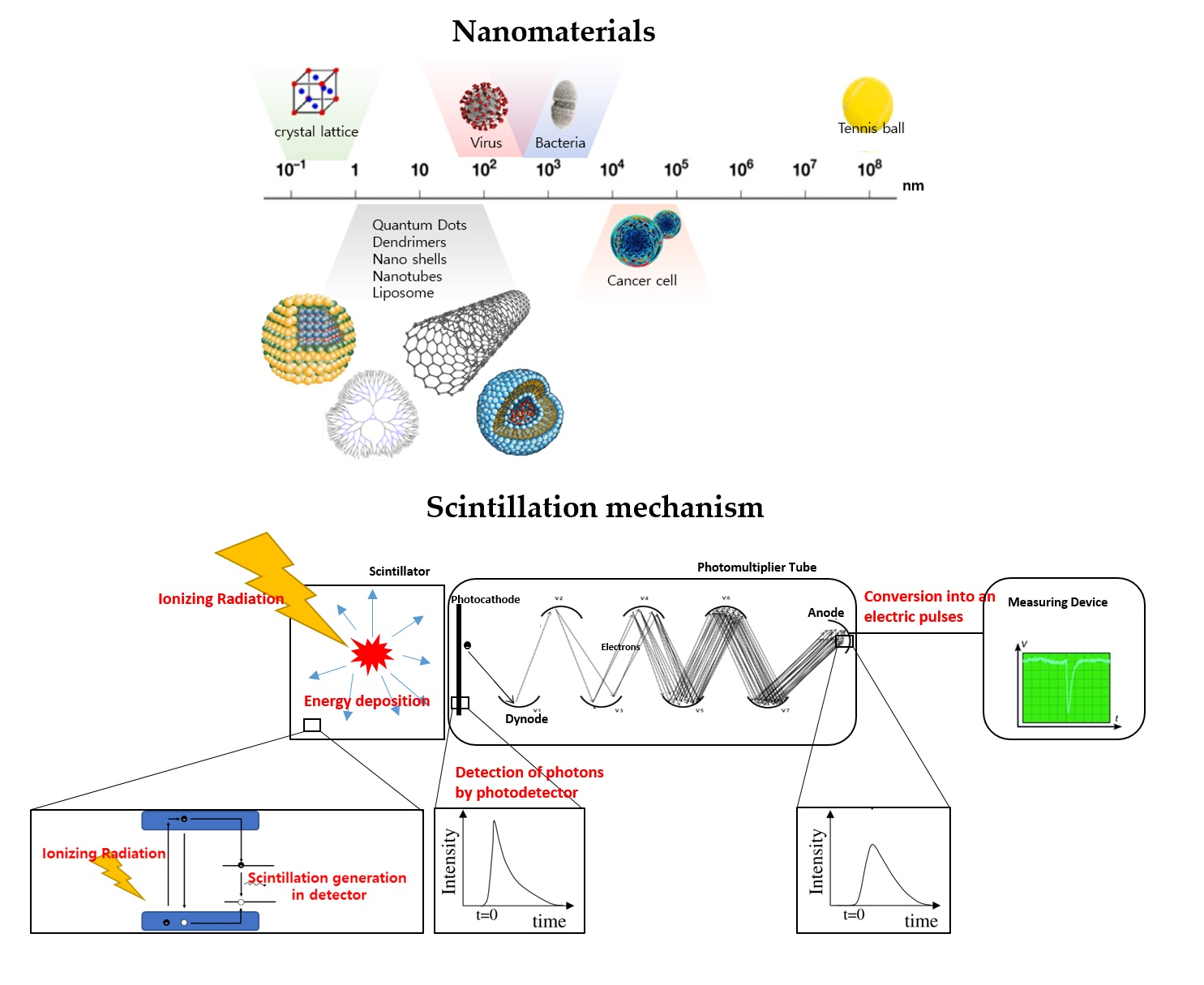
| Scintillator | NaI (Tl) | CsI (Tl) | BGO | CdWO4 | BaF2 | GSO | LSO | LuAlO3:Ce | YAlO3:Ce | RbGd2Br7:Ce | LaBr3:Ce | LaCl3:Ce | CaF2:Eu |
|---|---|---|---|---|---|---|---|---|---|---|---|---|---|
| Density (g/cm3) | 3.67 | 4.51 | 7.13 | 7.90 | 4.89 | 6.71 | 7.1 | 8.4 | 5.35 | 4.79 | 5.08 | 3.6 | 3.18 |
| Maximum emission wavelength (nm) | 415 | 550 | 480 | 470 | 310 | 450 | 420 | 365 | 390 | 420 | 360 | 350 | 435 |
| Decay time (ns) | 230 | 900 | 300 | 20,000 | 630 | 60 | 41 | 17 | 31 | 43 | 35 | 20 | 940 |
| Melting temperature (°C) | 661 | 621 | 1050 | 1325 | 1280 | - | - | - | - | - | 859 | - | - |
| Light yield (photon/MeV) | 40,000 | 52,000 | 8500 | 13,000 | 12,000 | 10,000 | 32,000 | 17,000 | 18,000 | 55,000 | 61,000 | 50,000 | 24,000 |
| FWHM at 662 keV (%) | 7 | 9 | 9.5 | 6.6 | 7.7 | 10.8 | 7.3 | - | 4.2 | 4.1 | 2.5 | 3.4 | 10 |
| Refractive index at emission wavelength | 1.80 | 1.78 | 2.15 | 2.25 | 1.5 | 1.91 | 1.81 | - | - | - | 1.9 | - | 1.44 |
| Deliquescence | O | O | X | X | X | X | X | - | - | - | O | - | X |
| Exciton Bohr Radius (nm) | Bandgap Energy (eV) | Mass Attenuation Coefficients * (662 keV, cm2/g) | Refs. | |
|---|---|---|---|---|
| Si | 43 | 1.11 | 0.0808 | [52] |
| Ge | 25 | 0.66 | 0.0745 | [52] |
| GaAs | 10 | 1.42 | 0.0748 | [52] |
| CdS | 2.8 | 2.58 | 0.0810 | [52] |
| CdSe | 6 | 1.74 | 0.0806 | [52] |
| ZnS | 5 | 3.68 | 0.0810 | [52] |
| PbS | 20 | 0.41 | 0.1248 | [52] |
| InP | 15 | 1.35 | 0.0785 | [53] |
| InAs | 34 | 0.35 | 0.0813 | [53] |
| InSb | 65.6 | 0.17 | 0.0815 | [53] |
| CdTe | 7.3 | 1.5 | 0.0806 | [53] |
| ZnSe | 4.5 | 2.67 | 0.0769 | [53] |
| Halide Perovskite | 2~5 | 1.5~3.1 | 0.0751~0.1277 | [54] |
| 2D Graphene | 3~8 | 0~0.55 | 0.0806 | [55,56] |
| Carbon nanotube(CNT) | 0.8~1.1 | 1.1 | 0.0806 | [57,58,59] |
* The values given in the table are approximate.
Table 3.
Advantage and disadvantages according to nanomaterial type [61].
Table 3.
Advantage and disadvantages according to nanomaterial type [61].
| 0D | 1D | 2D | 3D | |
|---|---|---|---|---|
| Type |
|
|
|
|
| Advantage |
|
|
|
|
| Disadvantage |
| |||
Table 4.
Top-down methods of nanomaterial synthesis [85].
Table 4.
Top-down methods of nanomaterial synthesis [85].
| Top-Down Method | Advantages | Disadvantages | General Remarks |
|---|---|---|---|
| Optical lithography | Long-standing, established micro/nanofabrication tool especially for chip production, sufficient level of resolution at high throughputs | Tradeoff between resist process sensitivity and resolution, involves state-of-the-art expensive clean room-based complex operations |
|
| E-beam lithography | Popular in research environments, an extremely accurate method and effective nanofabrication tool for <20 nm nanostructure fabrication with desired shape | Expensive, low throughput and a slow process (serial writing process), difficult for <5 nm nanofabrication |
|
| Soft and nanoimprint lithography | Pattern transfer based simple, effective nanofabrication tool for fabricating ultra-small features (<10 nm) | Difficult for large-scale production of densely packed nanostructures, also dependent on other lithography techniques to generate the template, and usually not cost-effective |
|
| Block copolymer lithography | A high-throughput, low-cost method, suitable for large-scale densely packed nanostructures, diverse shapes of nanostructures, including spheres, cylinders, lamellae possible to fabricate including parallel assembly | Difficult to make self-assembled nanopatterns with variable periodicity required for many functional applications, usually high defect densities in block copolymer self-assembled patterns |
|
| Scanning probe lithography | High-resolution chemical, accurately controlled nanopatterns in resists for transfer to silicon, ability to manipulate big molecules and individual atoms | Limited for high throughput applications and manufacturing, an expensive process, particularly in the case of ultra-high-vacuum based scanning probe lithography |
|
Table 5.
Bottom-up methods of nanomaterial synthesis [85].
Table 5.
Bottom-up methods of nanomaterial synthesis [85].
| Bottom-Up Method | Advantages | Disadvantages | General Remarks |
|---|---|---|---|
| Atomic layer deposition | Allows digital thickness control to the atomic level precision by depositing one atomic layer at a time, pin-hole free nanostructured films over large areas, good reproducibility and adhesion due to the formation of chemical bonds at the first atomic layer | Usually a slow process, also an expensive method due to the involvement of vacuum components, difficult to deposit certain metals, multicomponent oxides, certain technologically important semiconductors (Si, Ge, etc.) in a cost-effective way |
|
| Sol gel nanofabrication | A low-cost chemical synthesis process-based method, fabrication of a wide variety of nanomaterials including multicomponent materials (glass, ceramic, film, fiber, composite materials) | Not easily scalable, usually difficult to control synthesis and the subsequent drying steps |
|
| Molecular self-assembly | Allows self-assembly of deep molecular nanopatterns of width less than 20 nm and with the large pattern stretches, generates atomically precise nano system | Difficult to design and fabricate nano systems unlike mechanically directed assembly |
|
| Physical and chemical vaporphase deposition | Versatile nanofabrication tools for fabrication of nanomaterials including complex multicomponent nano systems (e.g., nanocomposites), controlled simultaneous deposition of several materials including metal, ceramics, semiconductors, insulators and polymers, high purity nanofilms, a scalable process, possibility to deposit porous nanofilms | Not cost-effective because of the expensive vacuum components, high temperature process and toxic and corrosive gases particularly in the case of chemical vapor deposition |
|
| DNA scaffolding | Allows high-precision assembling of nanoscale components into programmable arrangements with much smaller dimensions (less than 10 nm in half-pitch) | Many issues need to explore, such as novel unit and integration processes, compatibility with CMOS fabrication, line edge roughness, throughput and cost |
|
Table 6.
Nanomaterial doping and scintillator fabrication methods.
| Methods | Example Pictures | |
|---|---|---|
| Chemical Bath Deposition (CBD) | A method of depositing a substrate by immersing it in a liquid material |  |
| Ink-jet printing | A method of forming a uniform film on a substrate by finely spraying a liquid material through a nozzle |  |
| Spin coating | A method of forming a thin film using centrifugal force after placing a solution on a substrate and rotating it at a constant speed |  |
| Doctor blade | A method of forming a sheet by pouring the coating solution and passing the blade keeping a constant distance from the substrate |  |
| Irradiation | A method of polymerization by irradiating ionizing radiation with high energy such as gamma rays or X-rays |  |
| Thermal polymerization | A method of polymerization by heating without catalyst | |
Table 7.
Comparison of cps according to the concentration for quantum dot [98].
Table 7.
Comparison of cps according to the concentration for quantum dot [98].
| QD Conc. | 0 wt% (0 mg) | 0.04 wt% (1 mg) | 0.12 wt% (3 mg) | 0.2 wt% (5 mg) |
|---|---|---|---|---|
| Count rate(cps) | 976 ± 0.9 | 1640 ± 1.2 | 2570 ± 1.5 | 2990 ± 1.6 |
| Overall efficiency (%) | 0.75 | 1.26 | 1.97 | 2.29 |
Table 8.
The contents of CdTe/ZnS material used in the manufacture of plastic scintillators [100].
Table 8.
The contents of CdTe/ZnS material used in the manufacture of plastic scintillators [100].
| NO. | Styrene (wt%) | PPO (wt%) | POPOP (wt%) | QD (wt%) |
|---|---|---|---|---|
| 1 | ~99 | 0.4 | 0.01 | - |
| 2 | - | |||
| 3 | 0.4 | |||
| 4 | 0.1 | |||
| 5 | 0.05 | |||
| 6 | - | 0.1 | ||
| 7 | 0.05 |
Table 9.
Studies using nanomaterial-based scintillator or photodetector.
| Scintillator | Nanomaterial | Radiation | Methods and Results | Ref. |
|---|---|---|---|---|
| QD-based Plastic scintillator | CdS/ZnS QD and Styrene | γ-ray |
| [26] |
| QD-based Plastic scintillator | Perovskite and Epoxy | beta |
| [50] |
| PDMS coated Perovskite | Perovskite | X-ray |
| [71] |
| QD based Nanocomposite | Porus VYCOR and CdSe/ZnS QD | γ-ray |
| [74] |
| Polymer composite thin film doped with QD | Polyvinyl alcohol (PVA) polymer, CdTe QD and CdSe QD | X-ray |
| [75] |
| QD based Plastic(PVT) | CdZnS/ZnS (CZS) QD and FBtF QD | γ-ray |
| [76] |
| QD based Plastic(PVT) | CdS QD and VT(Vinyl toluene) | γ-ray |
| [77] |
| QD based plastic (styrene) | CdTe/ZnS QD, CdSe/ZnS QD and Styrene | X-ray |
| [78,79] |
| Nanocomposite | Graphene/CdTe/Au | X-ray andγ-ray |
| [80] |
| Carbon nanotube coated with a polymer | Single wall carbon nanotube (SWCNT) | γ-ray |
| [81] |
| nanocomposite | Perovskite, PMMA | X-ray |
| [85] |
| nanomaterial based flexible photodetector | Graphene, graphene oxide, and graphene QD |
| [82] | |
| 2D nano-semiconductor based photodetector | triphenylphosphine (PPh3), tungsten diselenide (WSe2) | Doping and lamination method |
| [83] |
| 2D material based photodetector | Silicon or indium gallium arsenide (InGaAs), Graphene, Graphene QD | Bonding methods |
| [84] |
Publisher’s Note: MDPI stays neutral with regard to jurisdictional claims in published maps and institutional affiliations. |
© 2021 by the authors. Licensee MDPI, Basel, Switzerland. This article is an open access article distributed under the terms and conditions of the Creative Commons Attribution (CC BY) license (https://creativecommons.org/licenses/by/4.0/).
Share and Cite
MDPI and ACS Style
Min, S.; Kang, H.; Seo, B.; Cheong, J.; Roh, C.; Hong, S. A Review of Nanomaterial Based Scintillators. Energies 2021, 14, 7701. https://doi.org/10.3390/en14227701
AMA Style
Min S, Kang H, Seo B, Cheong J, Roh C, Hong S. A Review of Nanomaterial Based Scintillators. Energies. 2021; 14(22):7701. https://doi.org/10.3390/en14227701
Chicago/Turabian StyleMin, Sujung, Hara Kang, Bumkyung Seo, JaeHak Cheong, Changhyun Roh, and Sangbum Hong. 2021. "A Review of Nanomaterial Based Scintillators" Energies 14, no. 22: 7701. https://doi.org/10.3390/en14227701
Note that from the first issue of 2016, this journal uses article numbers instead of page numbers. See further details here.