The Unified Power Quality Conditioner Control Method Based on the Equivalent Conductance Signals of the Compensated Load

Faculty of Electrical and Computer Engineering, Cracow University of Technology, 31-155 Cracow, Poland
Energies 2020, 13(23), 6298; https://doi.org/10.3390/en13236298
Submission received: 31 October 2020
/
Revised: 22 November 2020
/
Accepted: 24 November 2020
/
Published: 29 November 2020
(This article belongs to the Special Issue Industrial and Technological Applications of Power Electronics Systems)
Abstract
:This paper proposes a new control method for a Unified Power Quality Conditioner (UPQC). This method is based on the load equivalent conductance approach, originally proposed by Fryze. It can be useful not only for compensation for nonactive current and for improving voltage quality, but it also allows one to perform some unconventional functions. This control method can be performed by extending the orthodox notion of ‘static’ load equivalent conductance into a time-variable signal. It may be used to characterize energy changes in the whole UPQC-and-load circuitry. The UPQC can regulate energy flow between all sources and loads being under compensation. They may be located as well for UPQC’s AC-side as DC-side. System works properly even if they switch their activity to work either as loads or generators. The UPQC can operate also as a buffer, which can store/share the in-load generated energy amongst other loads, or it can transmit this energy to the source. Therefore, in addition to performing the UPQC’s conventional compensation tasks, it can also serve as a local energy distribution center.
1. Introduction
It is well known that distortions of supply voltage and load current cause power quality degradation, diminish the power factor of the supply system and may result in disruption of sensitive loads [1]. Shunt and series active power filters can alleviate these problems. Shunt filters are intended to compensate for load non-active current whereas series ones can improve supply voltage quality. The Unified Power Quality Conditioner (UPQC) can integrate advantages of both shunt and series active filters in order to achieve control over load voltage and source (line) current [2,3].
A wide review on UPQC configurations can be found in [3]. According to this classification the discussed UPQC can be classified as intended for a single-phase supply system that is based on a two-H-bridge converters employing the same DC-link capacitor. Depending on the point of injecting the compensating current with respect to the injecting transformer (Figure 1), the UPQC under study can be implemented as well in the UPQC-R (right-side shunt) as UPQC-L (left-side shunt) configuration. It is also classified as UPQC-P—It compensates source voltage sags using active power of supply sources. UPQCs can obtain reference signals on the base of frequency or time domain detection methods. Some researchers argue that “Harmonic current estimation is the key technology of power electronics systems to generate a harmonics reference current for harmonic control” and propose extensive and flexible solutions in this field [4]. Other researchers develop time-domain techniques [5,6]. Since the considered UPQC calculates references for load voltage and line current directly on the base of time variable quantities it can be classified as operating using time-domain signal analysis. In particular, this method refers to Fryze’s concept of the load equivalent conductance [7].
Commonly used control methods of UPQC involves continuous measurement of source voltage and load voltage and current in order to calculate reference signals for UPQC action. Such control methods are known as direct control techniques. However, UPQC can be steered using a somewhat different scenario, which may be classified as the indirect control method [8,9,10,11,12]. A type of the indirect method, which has been dubbed the conductance signal control method, has been successfully implemented to control the shunt active power filter (SAPF) action [9]. However, there is no implementation of this technique for UPQC so far. Applying the conductance signal control method references required to control the UPQC operation are obtained on the base of measuring the voltage across the UPQC’s DC-link capacitor. Since for this method the capacitor is employed as “a sensor” of load active power its voltage must not be controlled to be constant. On the contrary, the “freewheeling” capacitor voltage is measured and processed in order to obtain an equivalent (or hypothetical) conductance element that characterizes the consumption of the total active power taken from the source [8]. Since the load active power may vary in time, this conductance element should also be considered as time-dependent one. The ongoing information on conductance of this element may be referred to as the conductance signal. The first part of this paper shows that the conductance signal can be used to control the UPQC action.
As it turns out, if the conductance signal method is used some noteworthy additional functionalities of UPQC can be obtained. In particular, the UPQC can also be used to control the flow of energy between the supply source and the AC or DC passive or active elements of the network being connected with the particular UPQC. It can be said that in addition to perform the UPQC’s conventional tasks, it can also serve as a local energy distribution center operating with high power factor. This center may serve as a spot improving grid’s energetic efficiency. The second part of this paper describes these extra UPQC’s functionalities.
2. Control of UPQC with the Use of Signal of Load Equivalent Conductance
2.1. Basic Scheme of UPQC
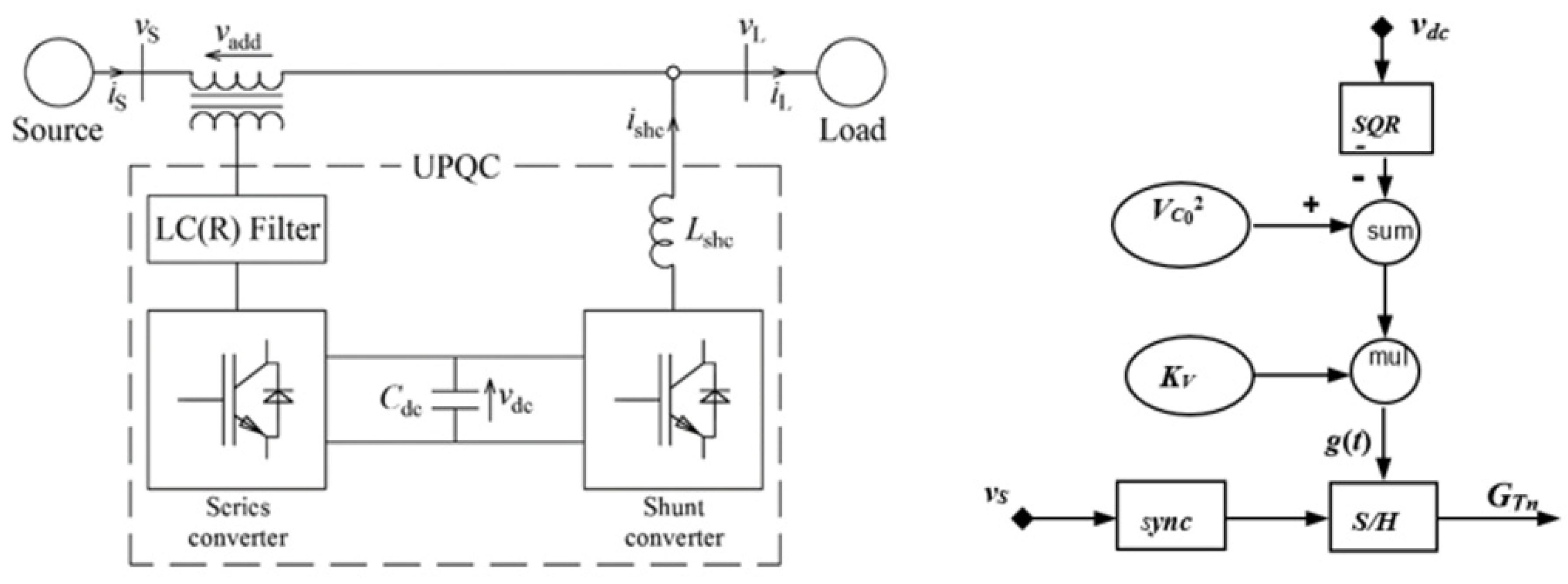
From the point of view of the studied control method the UPQC can be considered as composed of: (1) the shunt converter, which shapes source current iS to be active and of amplitude required to supply the load with the required active power and maintains the UPQC’s DC-link capacitor voltage in the assumed range, and (2) of the series converter, which tracks the supply voltage vS and—If needed—injects suitable voltage corrections vadd (Figure 1). As the result load voltage vL is shaped to be sinusoidal and of nominal amplitude. In the vast majority of cases the control circuitry of the UPQC’s shunt converter steers also the operation of the entire UPQC filter. The same rule is applied in this paper. A comprehensive review on the possible shunt converter control techniques can be found in [20,21].
2.2. Principle of UPQC’s Shunt Converter Control
The control unit of the shunt converter processes the voltage signal of the UPQC’s DC-link capacitor Cdc, Figure 1, in order to obtain the conductance signal. This signal gives crucial information needed to produce the reference for the source current. The conductance signal can be used to obtain the current reference signal as well for the shunt active power filter (SAPF) as for UPQC’s shunt converter.
In general, the compensated load may be nonlinear, time variable, passive or active, of single or polyphase structure with or without the neutral conductor, unbalanced, etc. From this perspective applying an universal method for obtaining the signal of equivalent conductance would be beneficial. Such an universal method, which allows this signal calculation as a function of amount of energy stored in the active filter’s reactance elements, has been proposed in [8]:
where: g(t) is the instantaneous load equivalent conductance signal; WAPF0 is initial amount of energy, which has been stored in all UPQC’s reactance elements during UPQC initialization procedure; wAPF(t) is amount of energy stored in these elements at instant t; NSF is the ratio of amount of energy delivered to the load from the supply source with respect to energy that is simultaneously delivered to the load from UPQC’s reactance elements—After each instant of change of load active power until the moment of achieving a new stead state by UPQC; Tst is a user dependent parameter that may be utilized to define UPQC time response on change of load active power; VS is source voltage rms.
The Equation (1) can be simplified to the form that only information on a part of total amount of energy stored in the UPQC is taken into account: namely that is stored in its DC-link capacitor:
where Cdc is capacity of DC-link capacitor, VC0 is its initial (i.e., after UPQC initialization procedure, see also WAPF0 in Equation (1)) voltage and vdc(t) is its voltage at instant t, and where:
It is characteristic for the discussed control technique that the DC-link capacitor voltage is not controlled to be constant. On the contrary, the “freewheeling” capacitor voltage is an input signal for obtaining the conductance signal. The KV factor gives a proportion between a signal related to the DC-link capacitor voltage and the conductance signal. The KV factor has a practical meaning: it may be used as the gain coefficient of a simple P-type regulator in the active filter’s control unit. No other signal converters of DC-link capacitor voltage are needed to obtain the conductance signal (Equation (2)).
There is a parameter Tst in the denominator of Equation (3). By changing this parameter the user can control the UPQC’s shunt converter inertial response on any change of load active power. By increasing/decreasing magnitude of this parameter more/less energy of each change of load active power can be buffered by DC-link capacitor. In other words, the Tst parameter can be used to regulate the energy flow between the source and the load in order to stabilize (or average) the source active power.
Having the conductance signal the reference for source current can be determined by the relationship:
where v1S(t) is fundamental component signal of source voltage. This component can be obtained in many ways (e.g., using filtration or PLL based techniques).
A variable component may appear in conductance signal (Equation (2)) if the load current contains a non-active component. Since UPQC compensates such component with the use of energy stored in its reactance elements (Equation (1)) this cause an oscillating component in DC-link capacitor voltage (Equation (2)). This component can distort the reference (Equation (4)). In order to eliminate impact of this component on the reference (Equation (4)) the continuous signal (Equation (2)) should be transformed into the stepwise waveform. To do this the signal (Equation (2)) is sampled at the very end of each subsequent period Tm of source voltage cycle. Then each sample is hold for the next period Tm+1, [8]. Application of such sample-and-hold procedure causes a “step-by-step” UPQC’s shunt converter action in that every change in load active power is practically entirely buffered with energy stored in the DC-link capacitor. For such method of full-buffering of energy flow the NSF parameter, see Equations (1) and (2), should be set to zero. As the result the source-to-load flow of energy is delayed for one period T and the stepwise form of the conductance signal applied for a Tm period is given by:
where: vdc(Tm-1) is capacitor Cdc voltage at the end of (m-1)th period T.
Finally, on the base of Equations (4) and (5) the source current reference signal iS* for period Tm is:
It should be emphasized that during compensation the following inequality has to be satisfied:
If this condition is not satisfied the UPQC dynamics can be insufficient. In an extreme case, when vdc(t) < vS(t), the UPQC action may become even harmful.
2.3. Principle of UPQC’s Series Converter Control
Source voltage waveform may deviate from its fundamental component due to wide range of physical phenomena existing in the grid. They may be considered as voltage harmonics, flicker, swell or sag, or pulse transients. There are specialized devices to overcome power quality problems that are related to voltage disturbances. The dynamic voltage restorer (DVR) seems to be the most economical solution in this field, [22]. However, UPQC’s series converter can maintain the load voltage vL to be close to the fundamental component v1S of the source voltage vS.
Independently of the reason of voltage distortion its shape bettering can be performed with the use of the same conductance signal-based control method considered. In other words, there is no need to identify the reason or spectrum of the source voltage distortion. In any case it is sufficient to inject the adequate voltage correction vadd in series with the source voltage vS (Figure 1). To produce appropriate voltage correction vadd the series converter generates (using energy stored in the DC-link capacitor) the current flow through the converter’s side winding of the injecting transformer. The hysteresis controller compares load voltage to its reference, i.e., the source voltage fundamental component, and steer switches action of the series converter in order to keep this voltage near this reference. As the result the required voltage vadd appears across the grid side winding of the injecting transformer.
Voltage and current distortion components may be considered as nonactive ones. Therefore, while compensating and being in the steady state, both UPQC converters impact the compensated voltage/current runs using nonactive power only, i.e., without change of mean magnitude of DC-link capacitor energy (if skip energy loss in the UPQC circuitry). In such situation the load conductance signal is still constant and, consequently, source current amplitude is constant as well. This observation is important from the perspective of the considered control method.
However, for the control method considered each change of load active power cause change of the conductance signal. Also energy losses in UPQC circuitry influence the total load-and-UPQC active power, so they impact the conductance signal (Equation (5)). It can be then said that there are no changes of signals (Equations (5) and (6)) when load active power is constant and the UPQC’s series converter compensates only for higher harmonics of source voltage. On the contrary, the signals (Equations (5) and (6)) get new magnitude when the series converter counteracts change of source voltage rms, or if there is a change in source voltage harmonic content. As a result the source is loaded higher/lower in order to maintain constant voltage rms across load terminals.
Finally, as an important conclusion it can be said, that all energy relations between the UPQC’s series converter and the rest of the system considered can be supervised by the control unit of the UPQC’s shunt converter and there is no operational incompatibility between both converters.
3. Studies for UPQC Standard Operation
The considered control method has been extensively verified by means of computer simulation. The IsSpice software (Intusoft, San Pedro, CA, USA) has been used. During some analyses performed the deformation of source voltage and load current often went beyond the voltage and current runs encountered in practice. They caused strong overload of UPQC circuitry. This approach, attractive in simulation studies, allows to assess the usability area of the considered UPQC control method.
In this paper simulation studies are divided into two parts. The first one, Section 3, considers UPQC standard operations, i.e., compensation for nonactive current and improving the voltage waveform on load terminals. The second part, Section 4, describes additional UPQC functionalities that arise if the conductance signal control method is used. In particular, this section considers the possibility of using UPQC as a distribution center for locally generated power.
For all analyses performed the same supply source characteristic and UPQC circuitry were used:
- (1)
- Supply source. Supply voltage waveform, vS in Figure 1, is composed of fundamental harmonic of rms 230 V/50 Hz and of two higher harmonics: rms 32 V/250 Hz and rms 32 V/350 Hz. Internal resistance and inductance of the supply voltage source is 2 mΩ and 100 μH, respectively.
- (2)
- UPQC’s shunt converter. Energy phenomena related to DC-link capacitor are essential for obtaining the UPQC reference signal. The capacity of UPQC’s DC-link capacitor Cdc is rated with respect to the maximal magnitude PLmax of the load active power and the Cdc capacitor maximal-to-minimal voltage ratio (compare Equation (7)). Thus, on the base of Equation (5) the needed capacity can be estimated as Cdc = 2PLmax/(VC02 − vdcT12). Finally, the initial voltage VC0 of 600 V and the Cdc capacity of 8 mF were used. A band-bang regulator operating with ∆I loop equal to 1 A has been used to force the reference current (Equation (6)). The inductance of shunt converter series inductor is set to 5 mH in order to limit the converter’s switching frequency to about 40 kHz. Switching elements of the converter are modeled to work similarly to IGBT transistors.
- (3)
- UPQC’s series converter. A hysteresis bang-bang regulator operating with ∆V equal to 5 V has been used to shape the load voltage waveforms near its reference signal: The fundamental harmonic component of source voltage. The inductance and capacity of the series converter’s LC(R) smoothing filter are designed so that the switching frequency of the serial converter is about 15 kHz.
- (4)
- Switching elements of the shunt converter are modeled in such a way that they work similarly to IGBT transistors.
- (5)
- A high-pass passive LC(R) filter has been added in parallel to the UPQC’s shunt converter in order to diminish flow of high-frequency component of the compensating current into the supply source branch.
3.1. Basic Examination of the Control Method. Turning UPQC and Load On and Off
Achieving the steady state after turning the UPQC or load on and off is considered in this Subsection. Analyses of selected signals of the network after switching the load on and off gives information on correctness of source-and-load energy balancing performed by UPQC. This energy balancing is crucial for the studied UPQC control method.
For all analyses carried out in this subsection the load is a thyristor power controller. It is composed of a 10 Ω resistor in series with two thyristors in antiparallel connection. Both thyristors are fired symmetrically with phase angle of π/2. This load brings in abrupt load power changes and wide harmonic spectrum for load current that can be difficult to compensate by SAPF and UPQC devices.
3.1.1. Turning UPQC’s Shunt Converter On
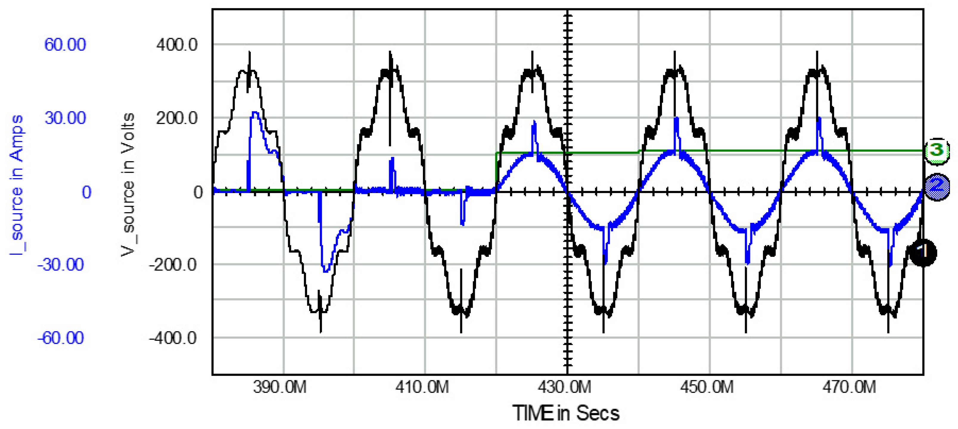
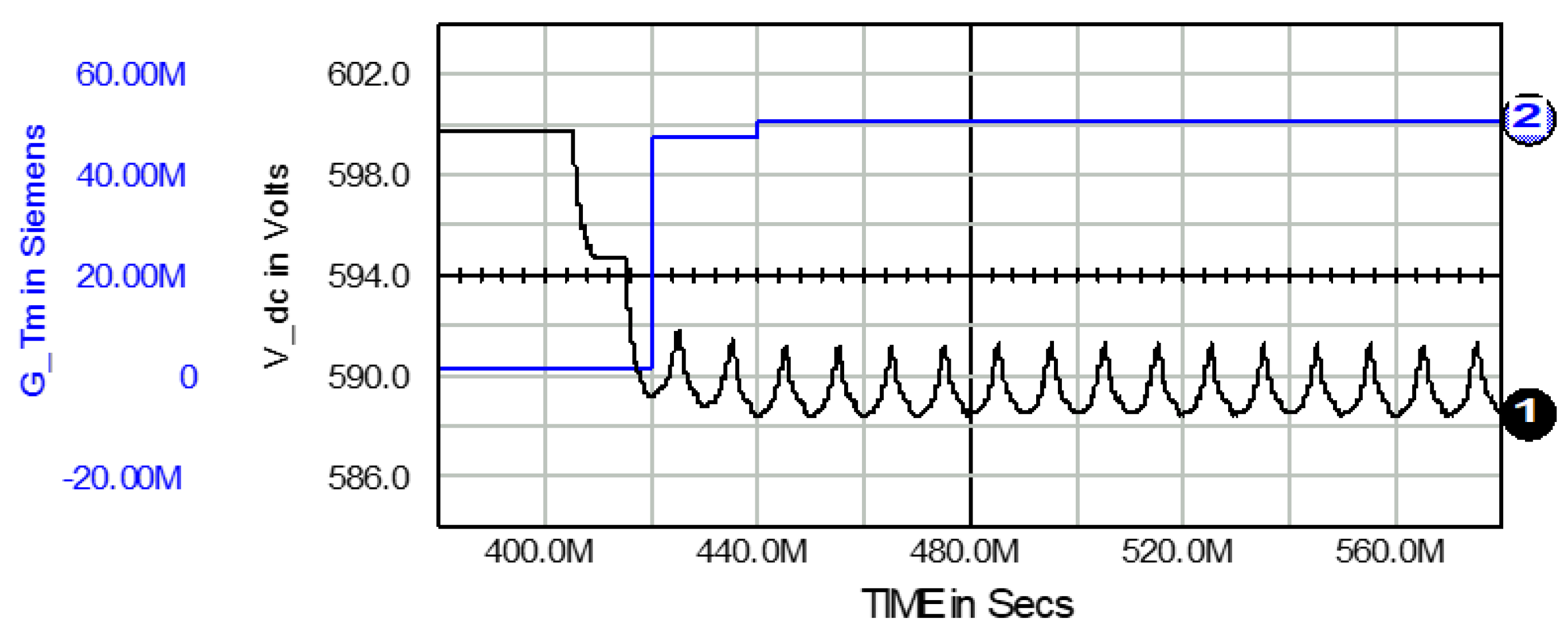
Since the shunt converter controls the source current it is also responsible for the total power delivered to the whole UPQC-and-load network. In particular, it controls also the source current component that is related to energy dissipated in all UPQC’s circuitry. For this reason the shunt converter should be turned on no later than the series one. The process of turning the shunt converter on is shown in Figure 2 and Figure 3, and then characterized with the use of basic electrical load and UPQC parameters collected in Table 1 and Table 2.
In Figure 2 source voltage vS(t), source current iS(t) and the conductance signal G(Tn)—According to Equation (5), are shown as waveforms 1, 2 and 3, respectively. Before the time instant t = 400 ms the source-and-load circuit acts in the steady state. The UPQC is inactive yet and does not impact the source-load energy transmission. Then the shunt converter is turned on at instant t = 400 ms. Until this moment the DC-link capacitor voltage is of its initial magnitude VC0, so the conductance signal (Equation (6)) is null. For that reason for the whole period T starting at this moment the load is powered using energy stored in UPQC reactance elements, practically solely from its DC-link capacitor. Therefore the source current is practically null. At the end of this period T, i.e., at t = 420 ms, the load equivalent conductance related to this period can be calculated and then used to produce the reference signal (Equation (6)) for the next period T, i.e., for time period 420 ms–440 ms.
The whole “static” change of the capacitor voltage takes place in two steps: the first step from 599.7 V (sample taken at time t = 400 ms), down to 589.3 V (sample taken at t = 420 ms) and then the second step from 589.3 V for sample taken at t = 420 ms down to 588.4 V at t = 440 ms. There are two main reasons of this two-step process of energy balancing:
- the first reason is due to intentional increasing the Tst parameter, see Equation (5). Setting this parameter to be longer then the period T introduces some inertia to the UPQC response on a change of source voltage or load power, making the UPQC action more stable. Here Tst has been fixed as increased by 2.2% with respect to the period T = 20 ms.
- the second reason is that energy stored only in the DC-link capacitor has been taking into account when calculating the conductance signal. In such case a comparatively small amount of non-considered energy, which is stored in other UPQC’s reactance elements, affects the conductance signal making it a little oscillating. This effect can be neglected because of possible load power changes for time-variable loads as well as possible random variations in source voltage.
Finally, after the two-step updating of the conductance signal magnitude the whole network achieves the steady state.
There are basic electrical parameters characterizing load and UPQC action, related to waveforms shown in Figure 2 and Figure 3, collected in Table 1 and Table 2. They characterize the load and source work, respectively.
The load work is buffered through the UPQC. Therefore, variations in load action are “seen modified” from the perspective of the supply source. In particular, there are two major changes, which are seen from this perspective, that occur in whole load-and-UPQC circuitry action at t = 400 ms and then 20 ms later. These changes are related to the periodical updating of the conductance signal, see Equation (5) and comments to Figure 2 and Figure 3.
It is noteworthy, that there is no difference in UPQC operation if the order of turning on the load and UPQC is reversed, that is, when UPQC is already active at the moment when the load begins its work. Similarly, at this moment the DC-link capacitor voltage equals its initial magnitude and the going magnitude of the conductance signal is zero. Consequently, the energy flow is buffered by UPQC with all consequences on UPQC action already described above.
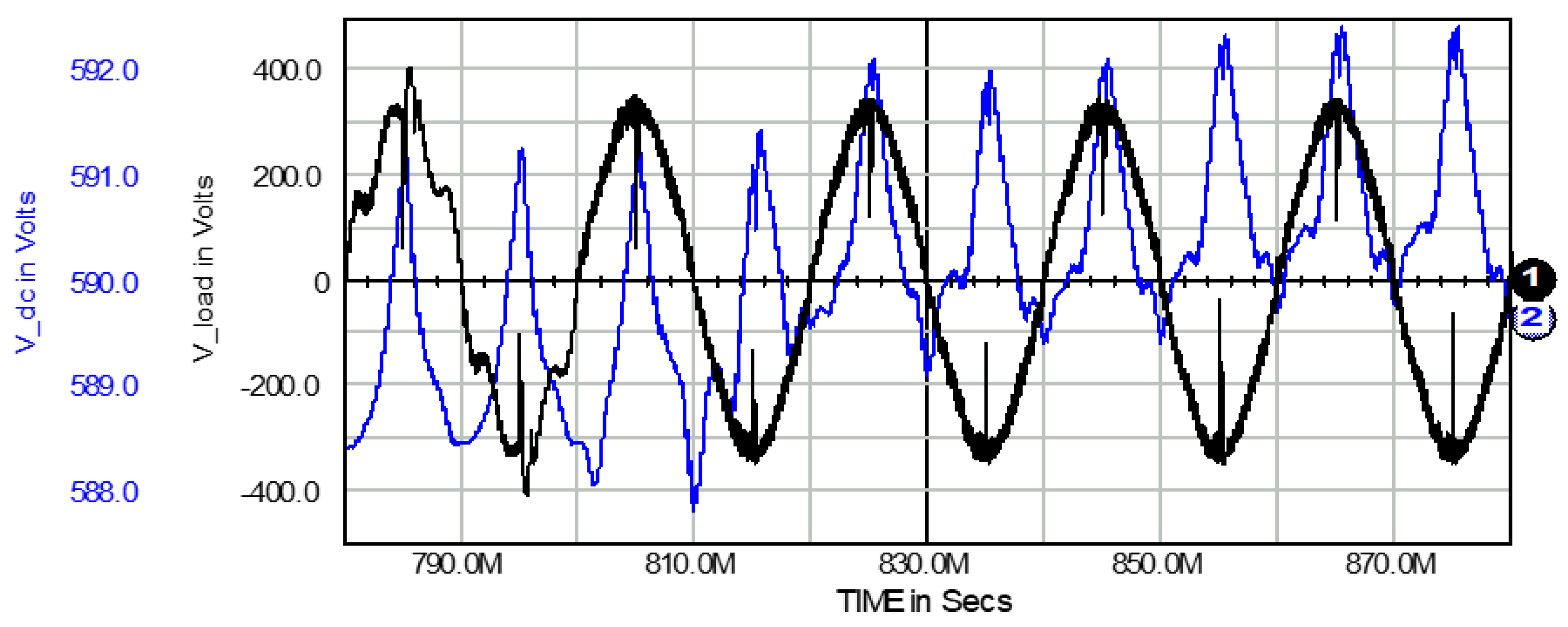
3.1.2. Turning UPQC’s Series Converter On
The series converter starts its action at t = 800 ms (Figure 4), when the network operates in the steady state and the shunt converter is already active. Since for the control method considered no time is needed for analysis of source voltage spectrum its distortion can be compensated immediately. This compensation cause change in harmonic components of DC-link capacitor voltage, waveform 2 in Figure 4. Although compensation for harmonics does not require the use of active power an increase of mean magnitude of the capacitor voltage can be observed. This is due to change of load active power being result of elimination of higher harmonics power from the total active power of the load.
Change in mean value of capacitor voltage causes change in magnitude of conductance signal (Equation (5)). Therefore, appropriate change of source current amplitude can be also observed. Changes of source-UPQC-load system parameters, related to Figure 4 and Figure 5, are collected in Table 3 and Table 4.
Just after turning the series converter on, at t = 800 ms, there is a drop of load active power resulting from eliminating load voltage distortion. As a consequence a part of source current turns out to be “excessive” with respect to going load and UPQC energy demand. Energy of this excessive current is stored in the DC-link capacitor increasing its voltage/energy. Therefore, on the base of Equation (5) the conductance signal is recalculated to a new magnitude at the beginning of the next T period. From this instant, i.e., for t = 820 ms, possibly delayed by the corrections described in the commentary next to Figure 2, the whole network reaches a new steady state.
3.1.3. Turning the Load Off
Before the load is turned off the whole network operates in the steady state. Then, at the moment t = 1400 s, the load is turned off (Figure 6).
Just after the load turning off moment the load current stops immediately. However, because of the energy flow buffering the flow of source current has been extended for the next period T, i.e., for the time 1400 s–1420 s (Figure 7 and Figure 8). As the result the whole circuit achieves zero steady state, i.e., with no load current/power, and UPQC is ready to the next compensation if load is turned on again.
3.2. Compensation for Source Voltage and Current Distortions
Beside compensation for voltage deformation from higher harmonics the UPQC should maintain sinusoidal load voltage even if source voltage is influenced by irregular or unexpected distortions. Source voltage swells and sags, flicker, and pulse-type distortions can be enumerated in this context.
In Section 3.2. the load consists of two branches in parallel. The first one contains a thyristor power controller, consists of a 15 Ω resistor in series with two thyristors in antiparallel connection operating with phase angle equal to π/4. The second one consists of 15 Ω resistor in series with 32 mH inductor. This load branch introduces reactive power into the network.
3.2.1. Compensation for Source Voltage Swell
The source voltage is composed initially of fundamental frequency component of rms 230 V and also of two harmonics: 32 V/250 Hz and 32 V/350 Hz. Then, beginning from t = 120 ms there is a swell of the source voltage fundamental component by 50%. The most important waveforms and electrical quantities are shown in Figure 9, Figure 10 and Figure 11, and then in Table 5 and Table 6.
The load operates in the steady state when at instant t = 80 ms UPQC’s shunt and series converters are activated simultaneously. For the first period T of UPQC operation, i.e., for time period 80 ms–100 ms, the load is powered practically solely with the use of energy stored in the DC-link capacitor, i.e., without drawing energy from the supply source. This cause decrease of DC-link capacitor voltage. Then, the first non-zero magnitude of conductance signal (Equation (5)) can be obtained at the very end of this time period, i.e., at instant t = 100 ms, waveform 3 in Figure 10.
At t = 120 ms the amplitude of source voltage fundamental component rises from 325 V up to 487 V, Figure 9. Since for the control method considered there is no time needed for analysis of source voltage spectrum this source voltage increase can be compensated immediately. The load voltage amplitude rises, but only to 349 V, Figure 9 and Table 5.
In order to compensate for this voltage increase a voltage correction is generated using energy stored in the DC-link capacitor. Depending on the voltage swell magnitude the current of the converter side of the series converter can reach significant values. This can result in significant increase of energy loss in this converter (Figure 11) and compare PLoad and PUPQC+Load in Table 5 and Table 6.
3.2.2. Compensation for Source Voltage Sag
The load operates in the steady state when the UPQC is turning on at t = 80 ms. At t = 120 ms the amplitude of source voltage fundamental frequency component decreases to 163 V. Due to the UPQC action the load voltage can be maintained on the amplitude about 295 V, Table 7 and Figure 12.
The source voltage drop is compensated with the use of energy drown from the supply source. This is performed as follows. The deficiency of source energy, caused by voltage sag, is balanced using of energy stored in the DC-link capacitor. As the result its voltage decreases. It causes an increase in the conductance signal (Equation (5)) and an increase in amplitude of the source current reference (Equation (6)). Source current rises increasing source active power (Figure 13). This “additional” source power is utilized to increase load voltage to be near its nominal magnitude.
Similarly to the case of voltage swell the compensation for voltage sag may require large current of the series converter. This imply a high magnitude of variable component of the DC-link capacitor voltage. If the instantaneous capacitor voltage falls close to the source instantaneous voltage, then UPQC may lose the possibility of correct operation. Therefore it can be said that in the analyzed case UPQC operates at the limit of its capabilities. This is illustrated in Figure 14, waveform 1.
It should be also noticed a problem of energetic cost of compensation for the source voltage sag. During compensation high current of the series converter causes a large dissipation of energy in its power circuitry. Such power loss can be estimated on the basis of a comparison of the active power at the load terminals against the active power at the UPQC’s input terminals: compare the parameter Pload in Table 7 with the parameter PUPQC+Load in Table 8.
3.2.3. Compensation for Source Voltage Fluctuations
Compensation for source voltage fluctuations within the range of magnitude of 0.9 to 1.1 of its nominal value and at frequency of 8 Hz is considered in this section. Such voltage fluctuation may be classified as flicker. Flickers cause a number of adverse effects in electrical circuits operation, for example for electric motors action electronic devices operation or lighting installations.
For the discussed UPQC control method, the way and effect of reducing flicker-type of source voltage fluctuations is identical with the method of compensating for source voltage swells and sags. In addition, because of smaller disturbances in source voltage amplitude they are easier for compensation. However, the flicker-type voltage oscillations can be considered as repetitive run in a narrow range of low frequencies. Therefore, it seems to be convenient to present here a distinctive way of the UPQC action which can be useful for such periodical-like voltage or current disturbances. In particular, the option of choosing a convenient value for the Tst parameter, see Equations (1) and (5), is utilized here. This possibility has been used to increase the inertia in UPQC operation against changes in load active power. Voltage fluctuations cause changes in this power. In general, the greater the magnitude of the Tst parameter the closer the conductance signal (Equation (5)) run with respect to its multi-period mean. As a result the source current (and load voltage) can be stabilized, so that flicker is easier to be reduced in the whole grid.
It should be noted, that if increase the Tst time the DC-link capacitor operates with lowered voltage. For this reason the condition (Equation (7)) may not be met. This can reduce UPQC dynamics or even cause UPQC operation to failure.
The UPQC operation when the time Tst is set to be equal to the source voltage period T, and then when it has been increased to 3T is analyzed. The conductance signal (Equation (5)) and DC-link capacitor voltage are shown in the same scale in Figure 15, respectively. It can be observed that for the Tst parameter increased to 3T fluctuation of conductance signal is reduced: Waveform 3 in contrast with waveform 1. Simultaneously the UPQC operates with lowered DC-link capacitor voltage: waveform 4 with respect to waveform 2.
The effect of flicker (and still existing harmonics) compensation for Tst = 3T is shown in Figure 16. The compensation can be considered sufficient. Taking into account that the load voltage amplitude is maintained to be constant, it can be concluded that the flicker compensation is sufficient.
4. Studies for UPQC Extended Operation
The extended functionality of UPQC is understood here as the possibility of using it also to control the energy exchange between all—Being influenced by given UPQC device action—Elements of the network. These elements may be of passive or active type or may be changeable from this point of view. There is no restriction on location in the network of these elements. They may be covered by UPQC extended action as well being located on the AC-side as on the DC-side of UPQC device. Therefore, beside compensating for undesirable components of grid voltage and current runs the UPQC can also serve as a local energy distribution center that can operate with high power factor. There is no change in UPQC circuitry parameters and in source voltage waveform components with respect to those introduced in Section 3. However, in order to highlight UPQC’s extended capabilities the load is composed to be nonlinear, time variable and of changeable passive or active kind.
4.1. UPQC Operation with Switched Passive/Active Work of AC-Side Load Elements
In general, there are two main possibilities of energy flow management when some nominally passive elements of load become generators and the amount of energy being generated in the load exceeds energy being consumed there:
- (a)
- the “excessive” amount of energy is transmitted up stream to the supply source or
- (b)
- the “excessive” amount of energy is stored in the DC-link capacitor.
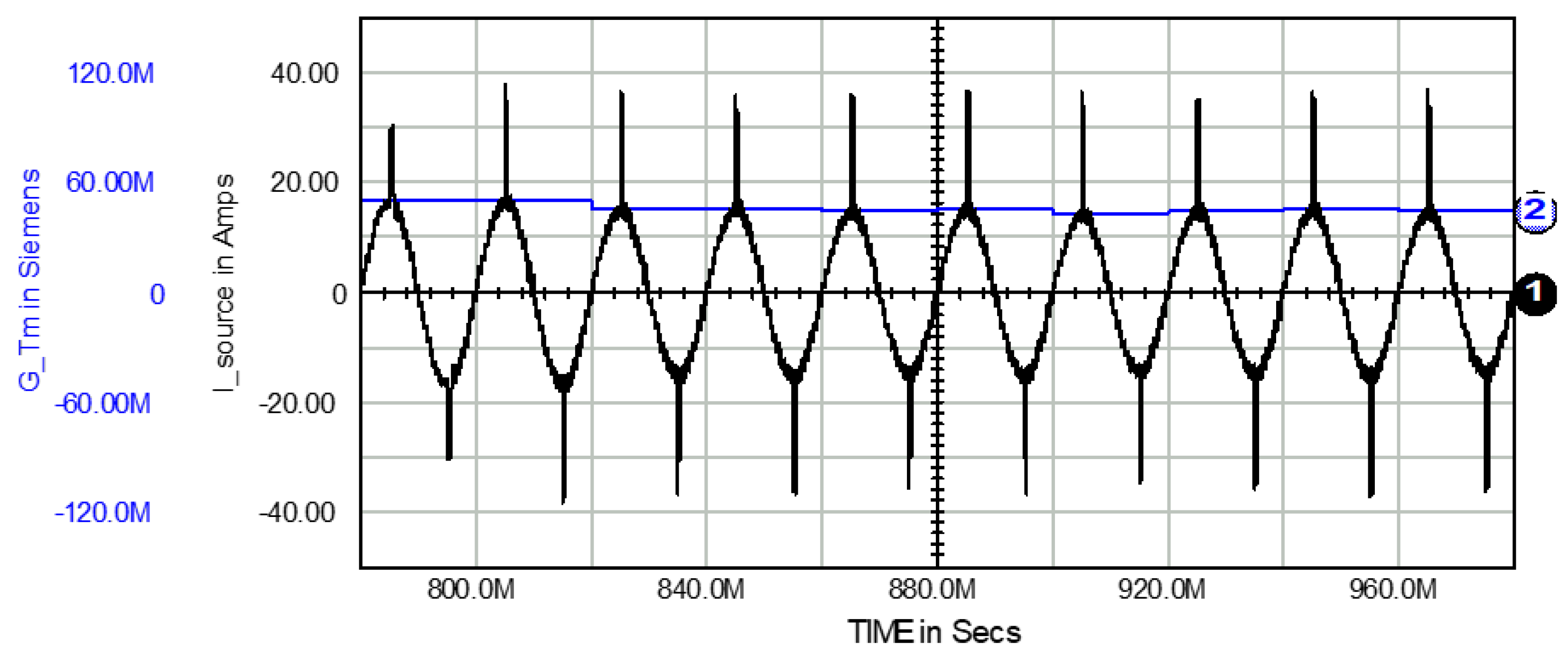
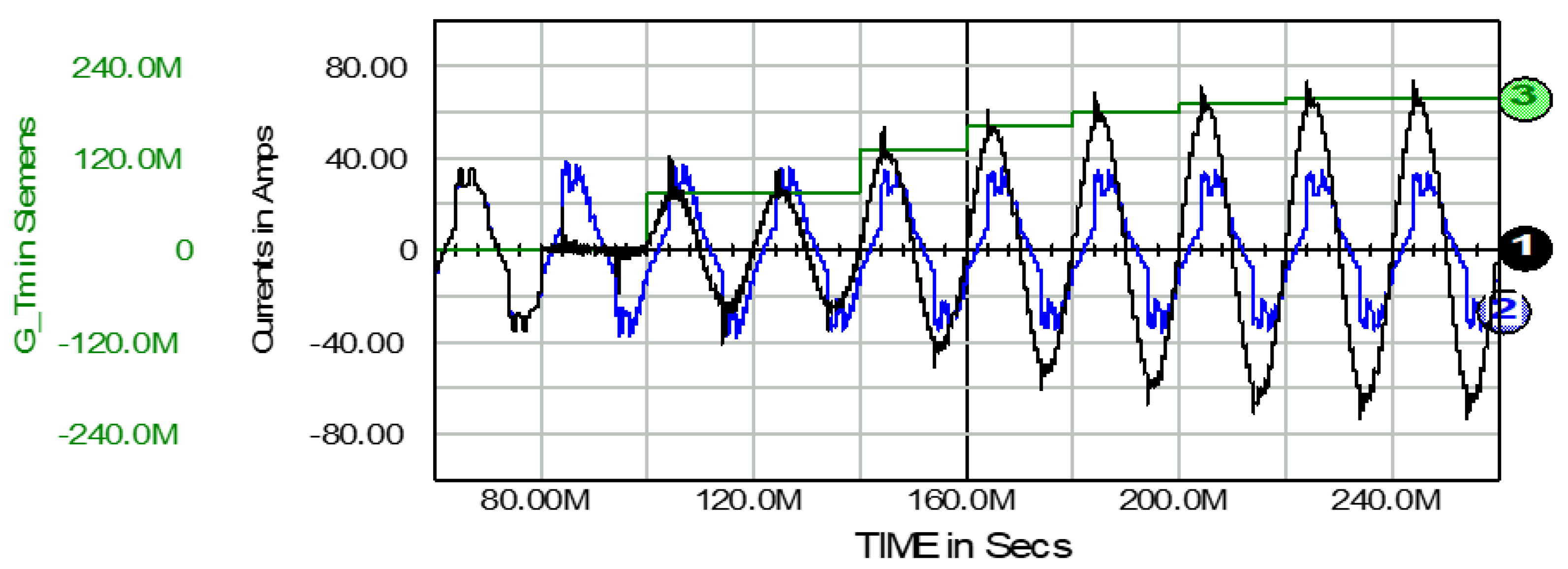
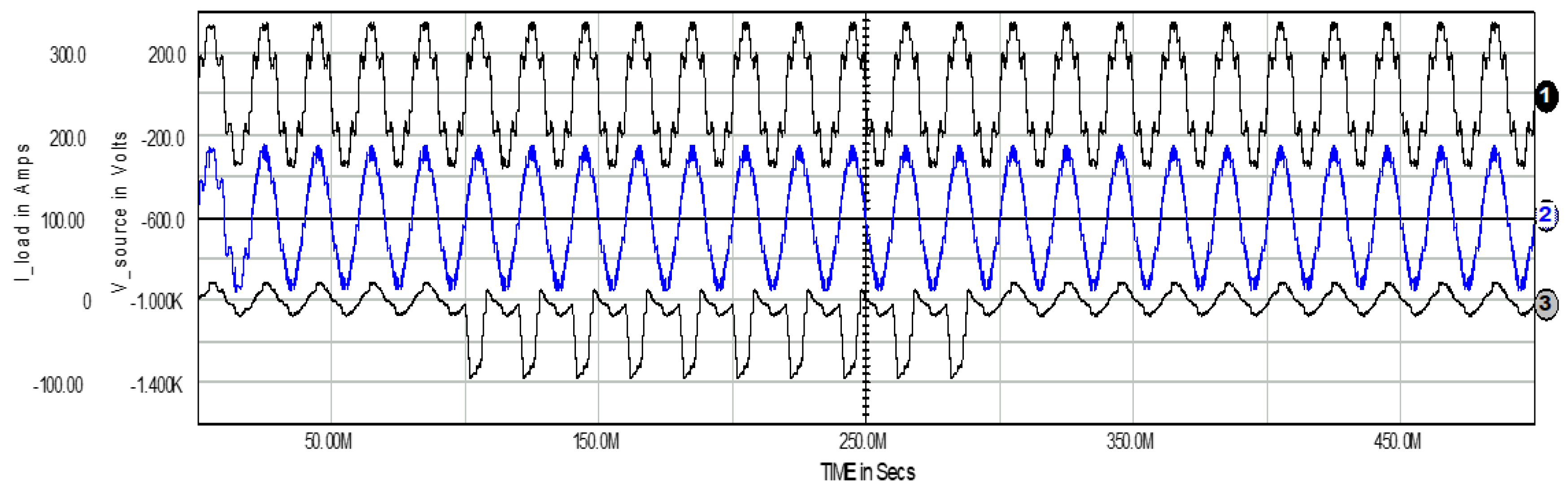
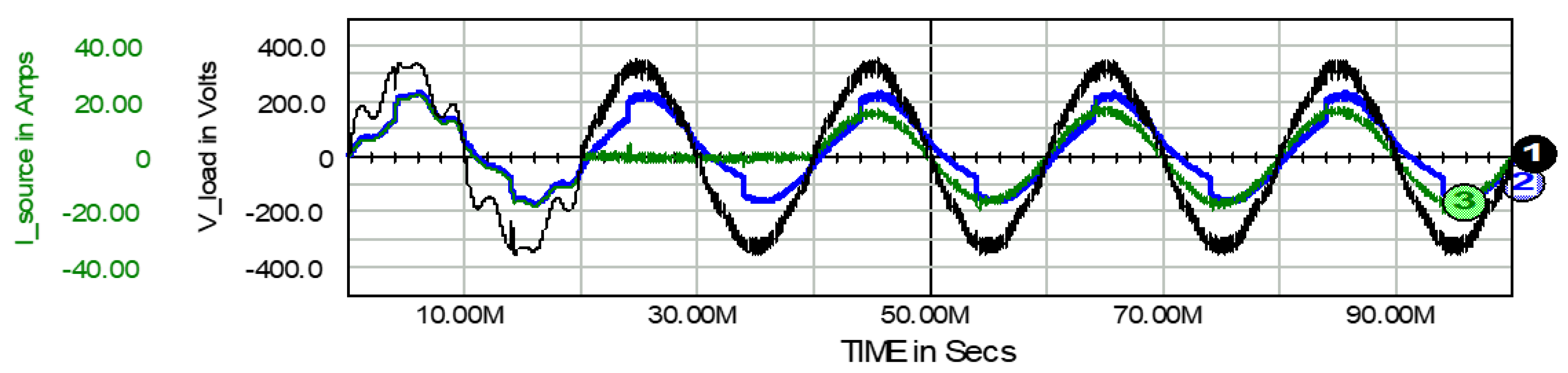
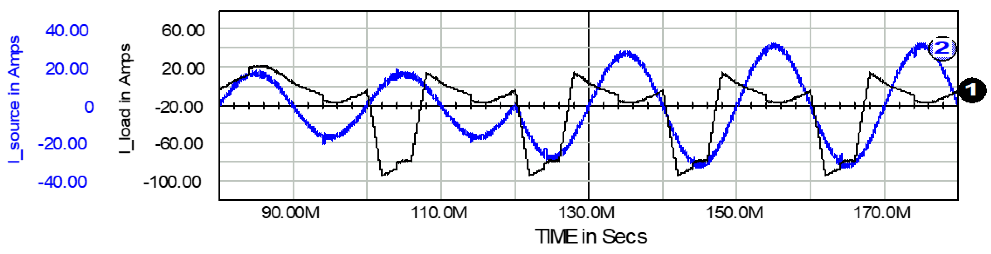
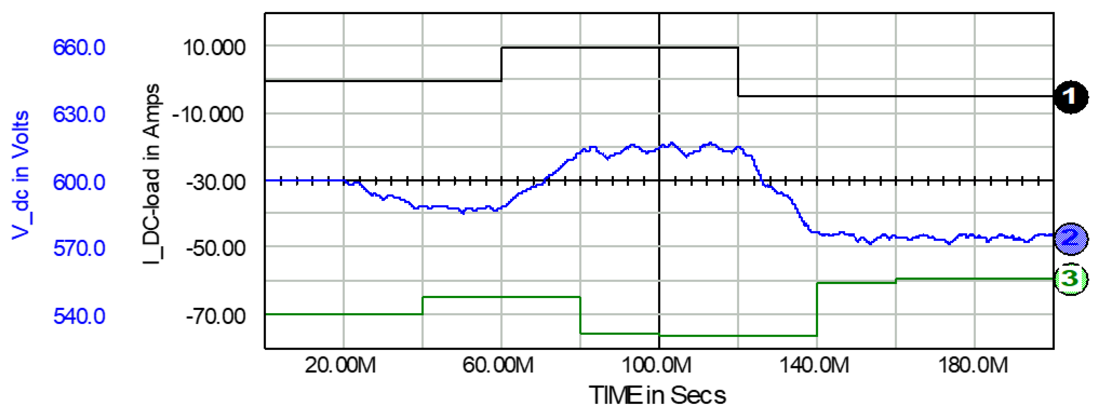
The case (a) may be realized in a full form, when all amount of the “excessive” energy is transmitted up stream to the source, or in a partial form, when some portion of the “excessive” energy is accumulated in the DC-link capacitor. Waveforms related to the (a) strategy are shown in a general outlook in Figure 17, Figure 18 and Figure 19, and then, in more precise look and with detailed comments, are presented in Figure 20, Figure 21 and Figure 22. Then, waveforms related to the (b) strategy are shown in general outlook in Figure 23 and Figure 24, and then are detailed in Figure 25, Figure 26, Figure 27, Figure 28 and Figure 29.
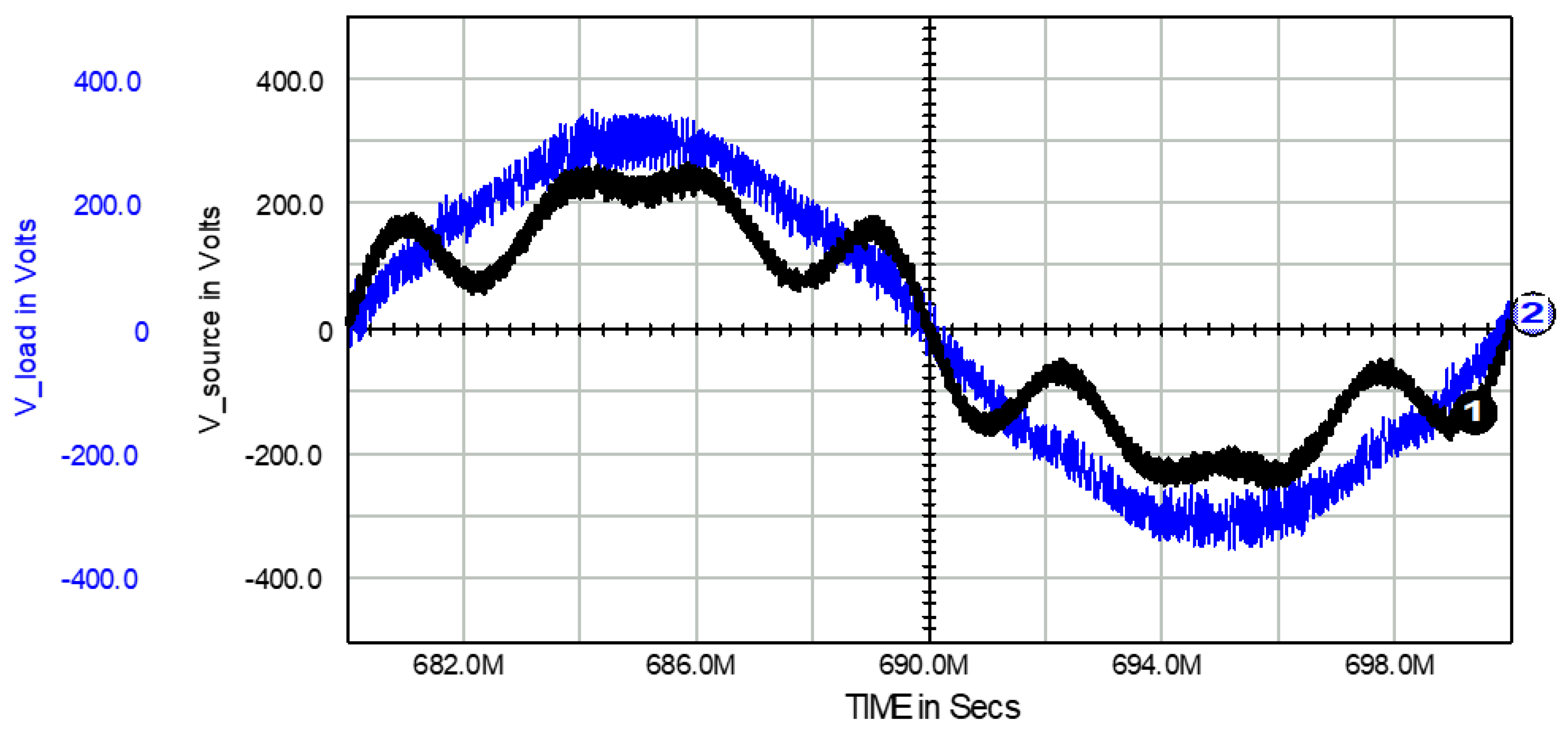
Figure 20 shows load voltage and current, and then source current during the first 100 ms of whole network action. This time period corresponds with the same time interval in Figure 17, Figure 18 and Figure 19, and then in Figure 23 and Figure 24.
The waveform 2 in Figure 20 is formed to represent total current of several loads, where some of them are nonlinear and time variable. The current is highly distorted, having also an inductive and DC components. Initially, in the time period T of 0 ms–20 ms the load active and apparent powers are 2.8 kW and 3.0 kVA, respectively, and 2.7 kW and 2.9 kVA during time period T of 20 ms–40 ms when UPQC starts its action.
Then, during the time interval 100 ms–300 ms, a new load-sided element was activated and therefore the load current run changes, see waveform 1 in Figure 21 (and waveform 3 in Figure 17). The load current is now composed to be almost unrealistically strongly distorted in order to show high and extended performance of UPQC. In particular a relatively large negative constant component of 17–28 A appears in the load current spectrum, so the fundamental frequency component is inverted relative to the fundamental component of the source voltage. Thus, the load, taken as a whole, works now as a source of energy. Because the in-load generated power exceeds both the power consumed in the load and dissipated in the UPQC the instantaneous DC-link capacitor voltage rises above its initial magnitude. As a result, the conductance signal changes its sign to negative, see waveform 3 in Figure 18. Consequently, the source current, still being purely active, begins to be controlled by the UPQC’s shunt converter in order to carry some amount of the in-load generated power to the source, waveform 2 in Figure 21.
Estimation of energy balance in the network when it is practically in the steady state (here in the time period 200 ms–220 ms, when there is no change in the load power and in the static DC-link capacitor voltage, see Figure 17 and Figure 18) is as follows: in-load generated power: 7.85 kW, in-load consumed power: 2.72 kV, power transmitted from the load to the source: 5.07 kW, power dissipated in UPQC’s shunt converter: 43 W and power dissipated in UPQC’s series converter: 226 W. From this energy balance results that the in-load generated power feeds passive elements of the compensated load and covers UPQC’s energy loss. The remaining “excessive” amount of in-load generated power is transmitted to the source.
After switching off the in-load generating element the DC-link capacitor voltage diminishes below its initial magnitude. For this reason the conductance signal becomes positive, consequently source current polarity has been inverted and load draws energy from the source again. This is shown in Figure 18 and Figure 22.
During the time period about 100 ms–350 ms the UPQC operates as a compensator as well as an energy distributor. Note, during this time load voltage and source current were maintained to be sinusoidal, irrespective of energy flow direction (Figure 17 and Figure 18).
4.1.1. Split Storing/Distributing of the In-Load Generated Energy
As it was already stated the energy generated in the active part of load may be decomposed into the portion consumed immediately and into the “excessive” portion. In turn this “excessive” portion may be split into a piece to be transmitted immediately to the grid and a piece to be stored in the DC-link capacitor. In other words, a power limit may be imposed on energy transmission to the grid (or, if needed, a voltage limit may be imposed on maximal DC-link capacitor voltage).
Such possibility of limited back-transmission is illustrated in Figure 19. In this example the maximal back-transmission power is bounded to 2.7 kW. Because the in-load generated power is greater than the allowed power limit of the back-transmission the DC-link capacitor voltage (energy) rises. It lasts till the moment of switching-off the generating element that is located in the load. Then the “excessive” energy portion, which were stored in the capacitor, is discharging partially to the source and partially to UPQC—Being dissipated in its power circuitry. After achieving the balance between load and source active powers, what can be seen in Figure 19 about t = 380 ms, the source takes over powering the load.
4.1.2. Full Storing of the In-Load Generated Energy
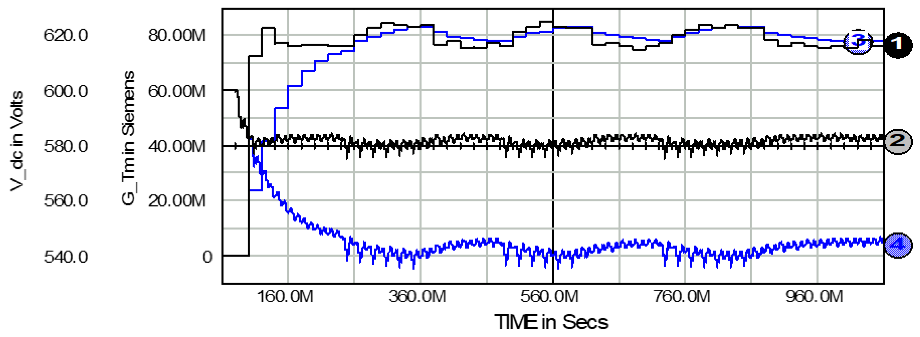
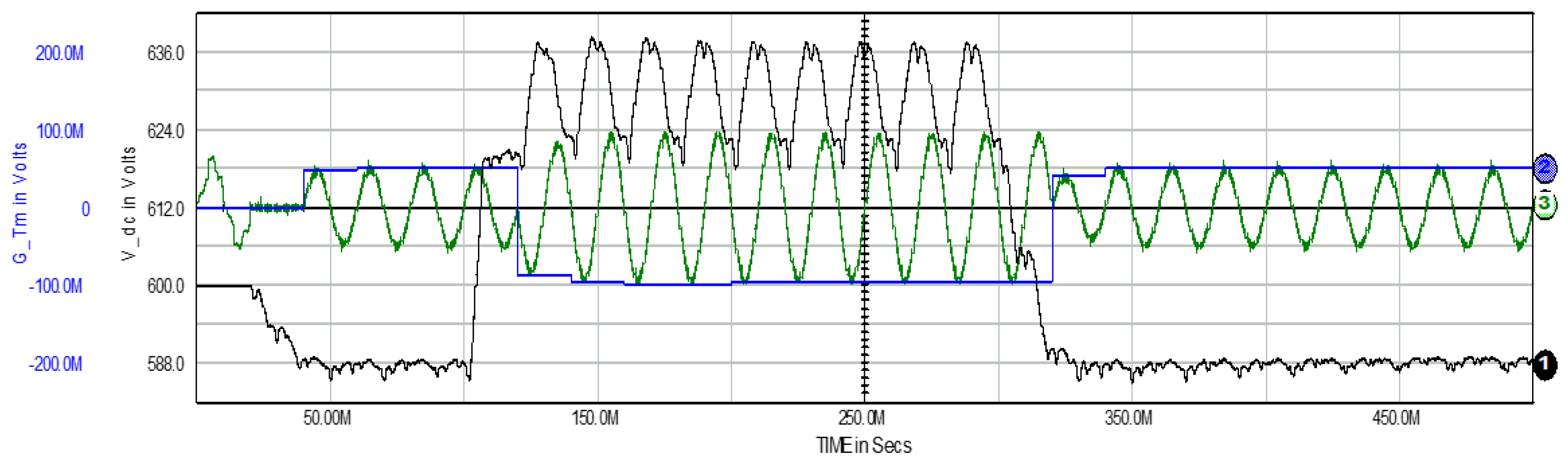
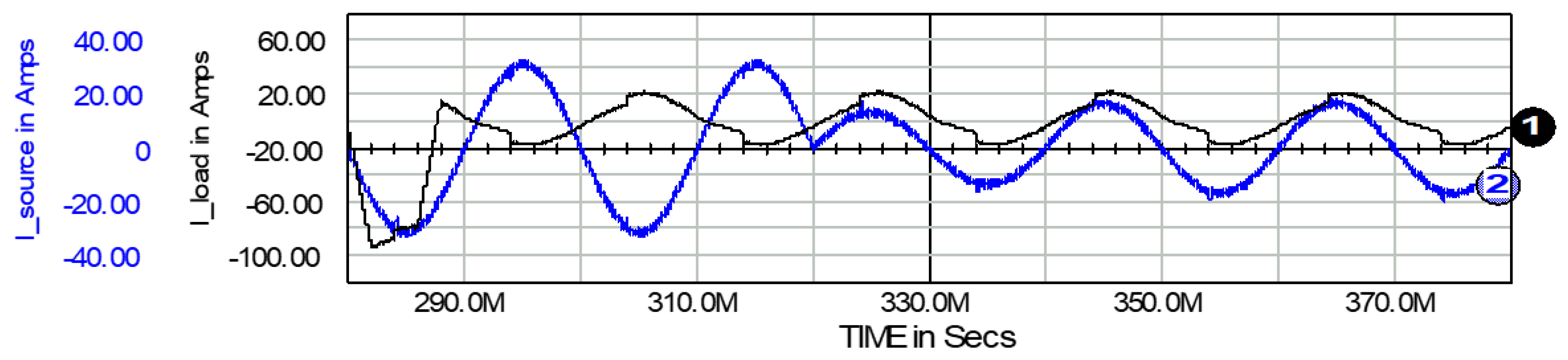
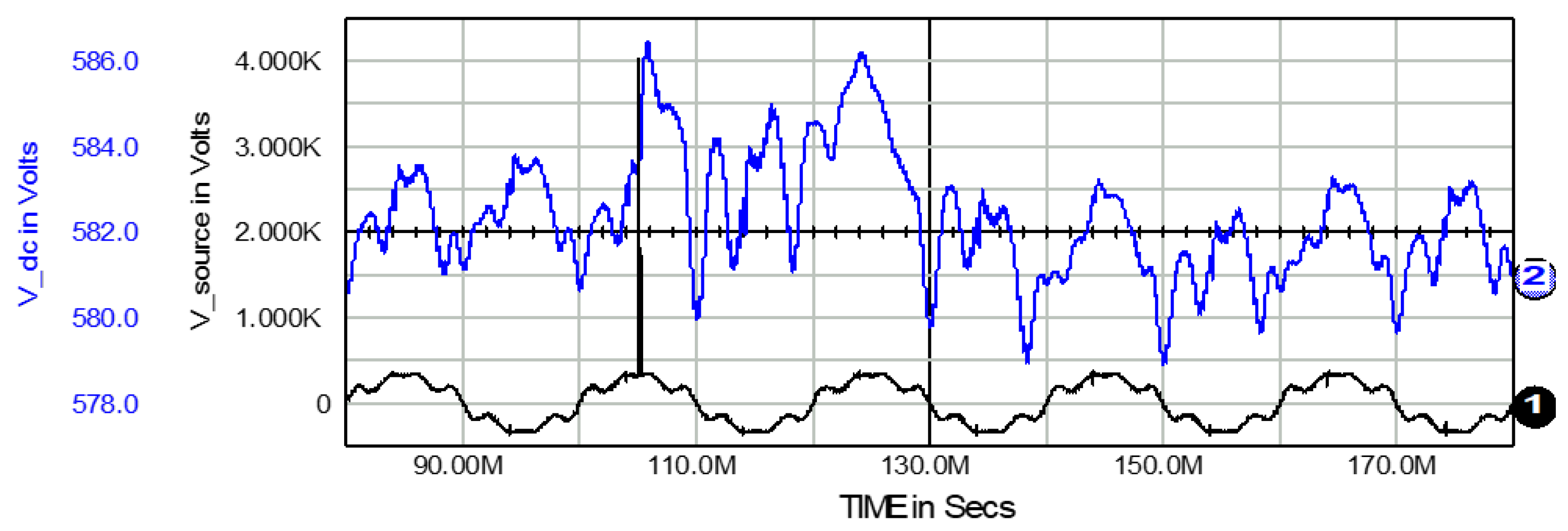
Characteristic waveforms of currents and voltages for the case of the full energy-storing mode (without upstream energy transmission) are shown in general outlook in Figure 23 and Figure 24, and then some critical time areas are zoomed in Figure 25, Figure 26, Figure 27, Figure 28 and Figure 29.
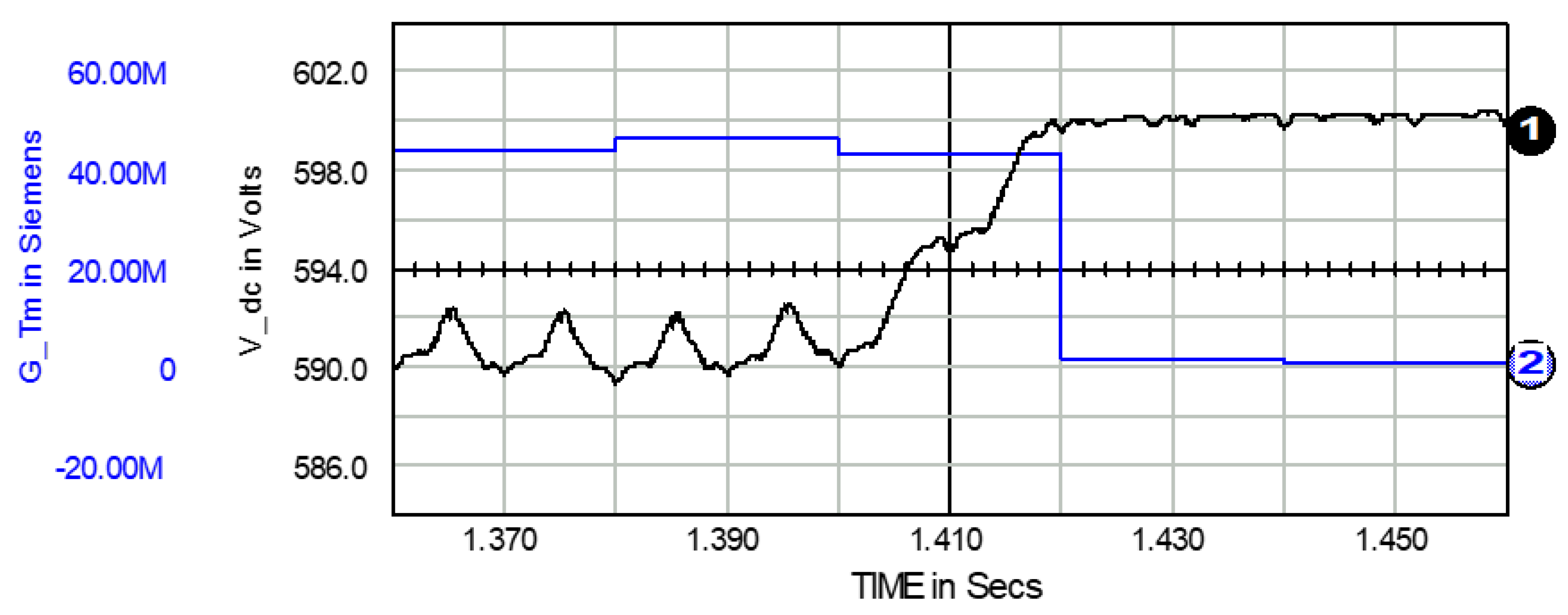
The waveform 1 in Figure 24 demonstrates the process of accumulating/discharging the in-load generated “excessive” energy in the DC-link capacitor. The energy accumulation process takes place in time periods 180 ms–340 ms and then 540 ms–620 ms, whereas the energy discharging can be seen during time periods 340 ms–520 ms and 620 ms–940 ms. These time intervals fall within the wider 180 ms–940 ms range in which UPQC’s shunt converter blocks any current flow to-or-from the supply source. In other words, during the time 180 ms–940 ms the load works in an energetically autonomous way, that means without any energy drawing from or giving to the supply source. Power fluctuations of all elements of the network are buffered by UPQC. Simultaneously all UPQC’s conventional compensation tasks are fully fulfilled.
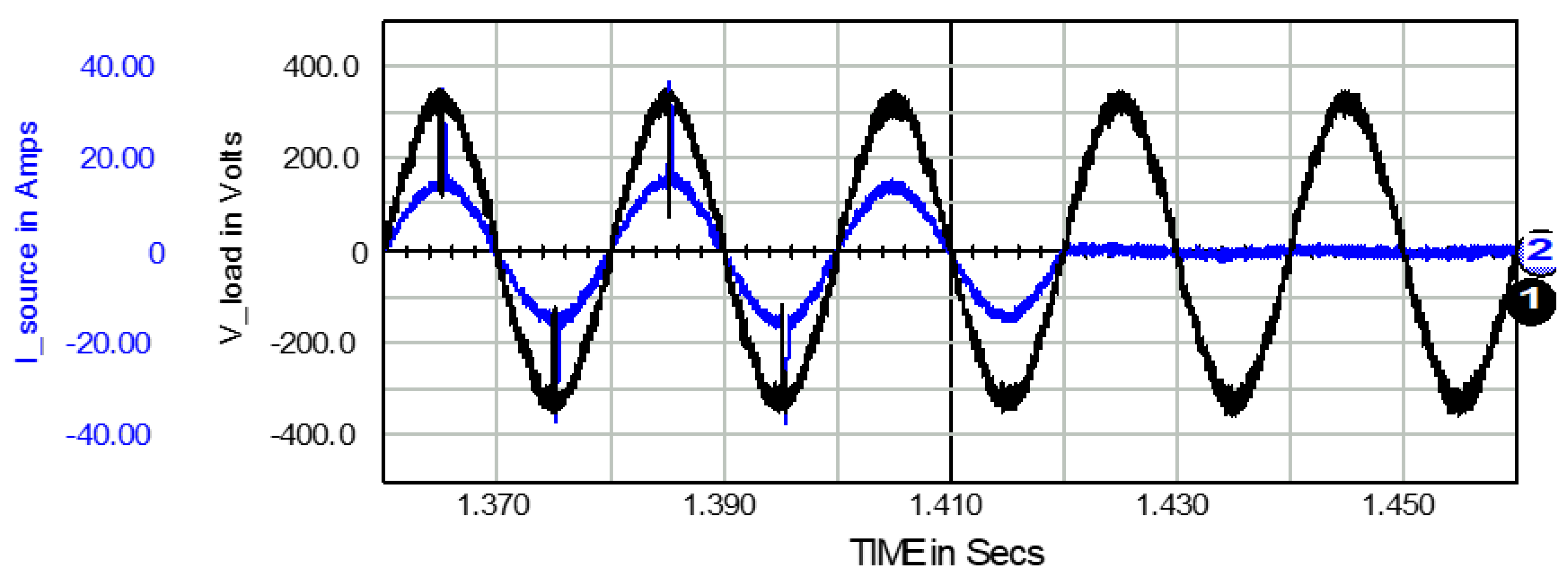
The most critical areas occurs about 200 ms–300 ms and then about 550 ms–600 ms. There is a cumulation of strong source voltage harmonics distortions with voltage swell and later with voltage sag. There are also large load current deformations, including high energy negative pulses that generates “asymmetrical” active power, occurring only during positive half-waves of source voltage.
The 240 ms–260 ms T period was chosen to show the effect of UPQC action (Figure 25).
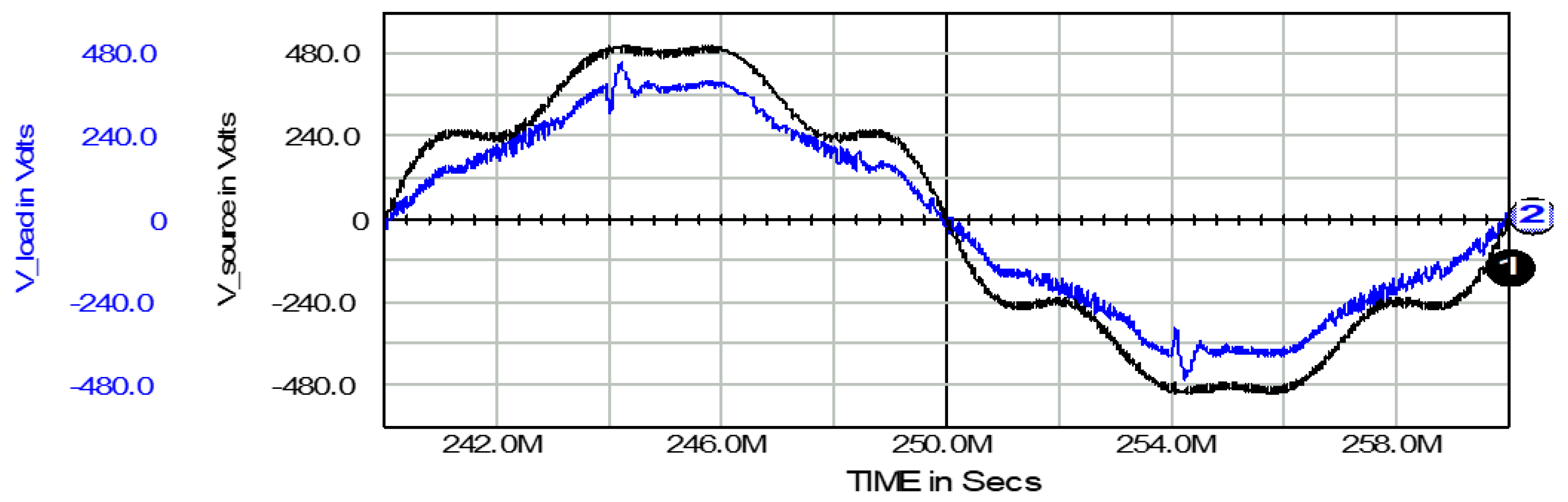
For this period the RMS and THD parameters of source voltage run have been reduced at load terminals from the “swelled” magnitude of 348 V down to 268 V and from 14.7% to 7.7%, respectively. Unfortunately, it can be said that despite a significant improvement of load voltage parameters, the voltage quality requirements have not been met.
Within the second critical area the 580 ms–600 ms T period was chosen to show the effect of UPQC action (Figure 26). For this period the RMS and THD parameters of source voltage waveform have been improved at load terminals from the “sagged” magnitude of 162 V up to 219 V and from 32.7% down to 4.1%, respectively. It can be said that these parameters may be considered satisfactory.
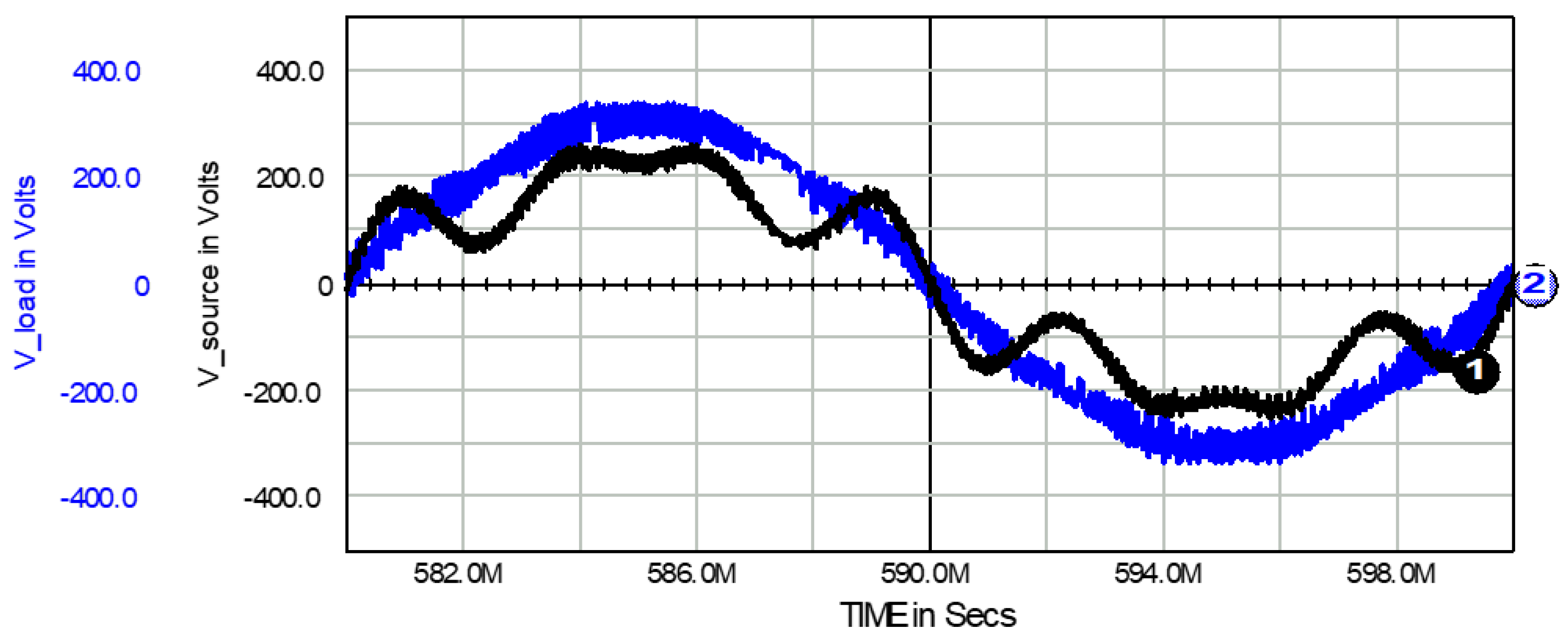
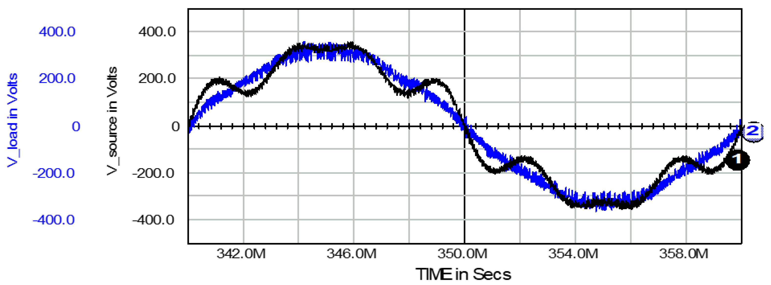
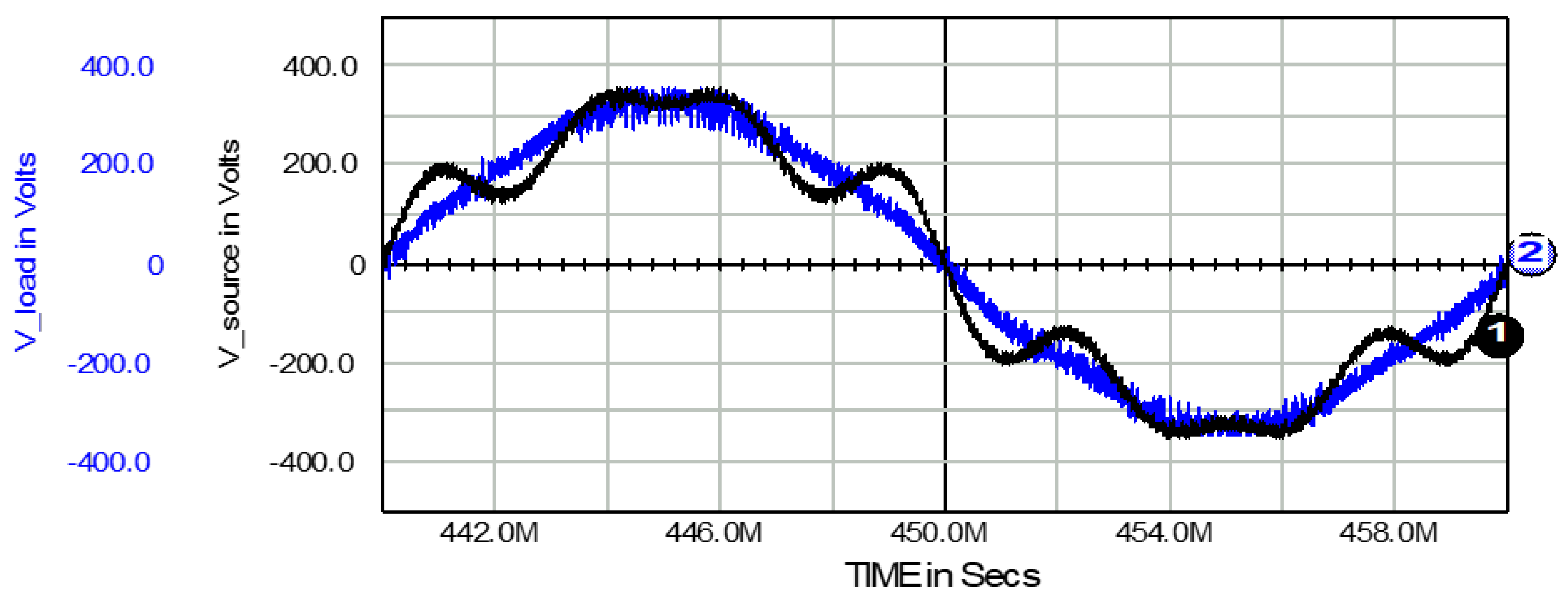
The source and load voltages for non-critical areas are presented in next three figures. The 340 ms–360 ms, 440 ms–460 ms and 680 ms–700 ms T periods were chosen to show these waveforms in Figure 27, Figure 28 and Figure 29, respectively. The load voltage RMS and THD parameters can be accepted as sufficient from the voltage quality point of view. In particular, there is no significant difference in the content of harmonics when working with or without compensation for source voltage sag.
4.1.3. A Side Effect of Conductance Signal Control Method: Alleviating and Catching Energy of Source Voltage Spike Distortion
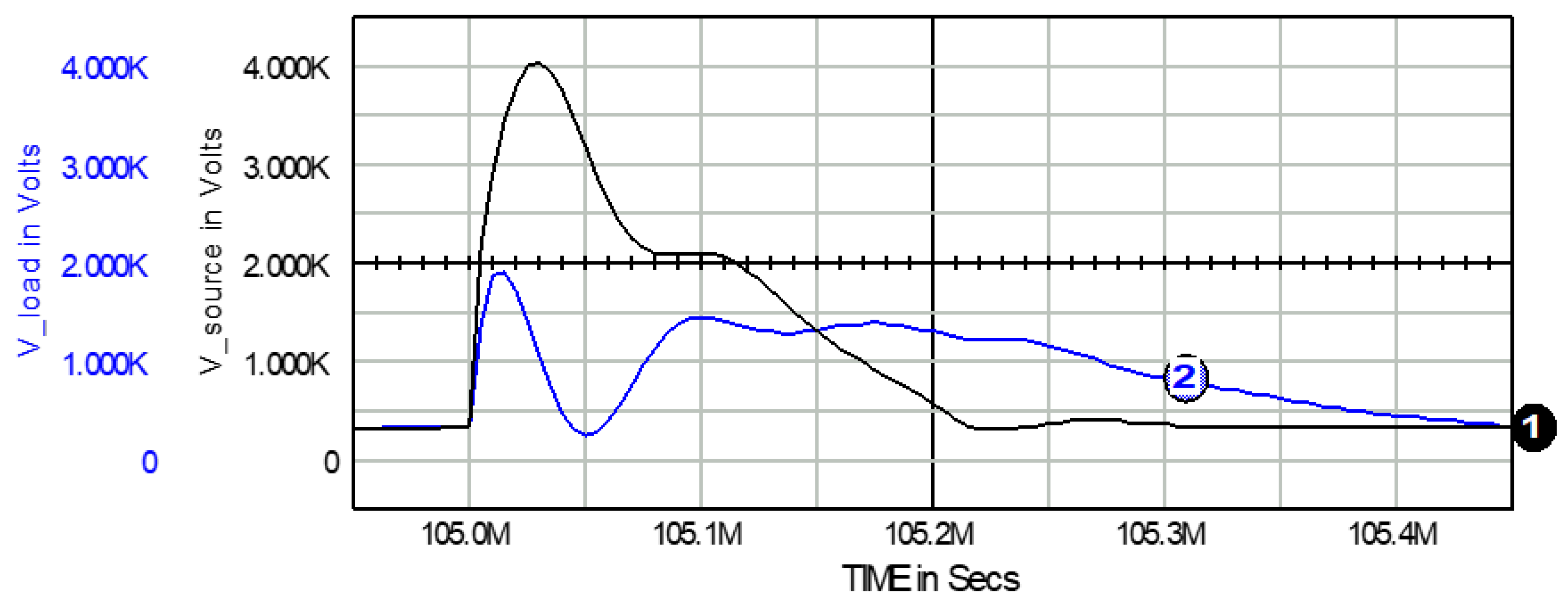
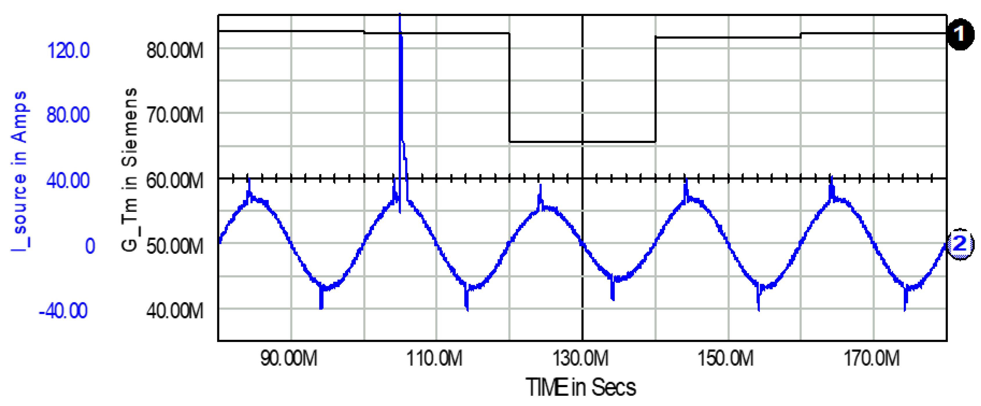
From time to time an impulsive voltage transient (voltage spike) can appear in the grid, e.g., as a result of lighting stroke. Lighting arresters can be used to stop the transient. Fortunately, it follows from the principle of the considered control method that UPQC can alleviate, or even store and then utilize some amount of energy of such voltage distortion.
The network operates in the steady state when a voltage spike appears at t = 105 ms, Figure 30. Parameters characterizing this spike are 3.3 kV in magnitude, 1.2 μs rise time, 10 μs peak voltage duration and 200 μs fall time.
Energy of this source spike increases amount of energy, which flows through UPQC input terminals, from 89.9 J during the stead state T period 80 ms–100 ms, up to 141.6 J for the next (i.e., hit by the spike) 100 ms–120 ms T period. Some amount of energy of the spike impacts the load immediately, what can be seen as load voltage distortion shown in waveform 2 in Figure 31. As the result, the energy consumed by the load rises from 88.2 J for the 80 ms–100 ms time period up to 125.4 J for the next one. However, some portion of energy of the spike has been caught by UPQC. This energy portion increases energy stored in the DC-link capacitor: note the difference in capacitor voltage between instants t = 120 ms and t = 100 ms in waveform 2 in Figure 30.
Because UPQC buffers energy variations between the supply source and the load the energy of the pulse distortion, which reaches load terminals, is lower than the distortion of energy that appears on UPQC input terminals. This is 125.4 J with respect to 141.6 J, respectively. This energy difference increases electric charge stored in the DC-link capacitor and, at the same time, increases its static voltage from 581 V at t = 100 ms up to 584 V at t = 120 ms, waveform 2 in Figure 30. This “additional” voltage (or energy) decreases the conductance signal (Equation (1)) from 82.3 mS for T period 100 ms–120 ms down to 65.7 mS for the next T period 120 ms–140 ms, waveform 1 in Figure 32. This fall of conductance signal (Equation (1)) causes decreasing in source current amplitude from 26.6 A down to 21.3 A, waveform 2 in Figure 32 during the T period 120 ms–140 ms. In other words, during this T period UPQC uses the from-the-distortion energy to power both itself and the load.
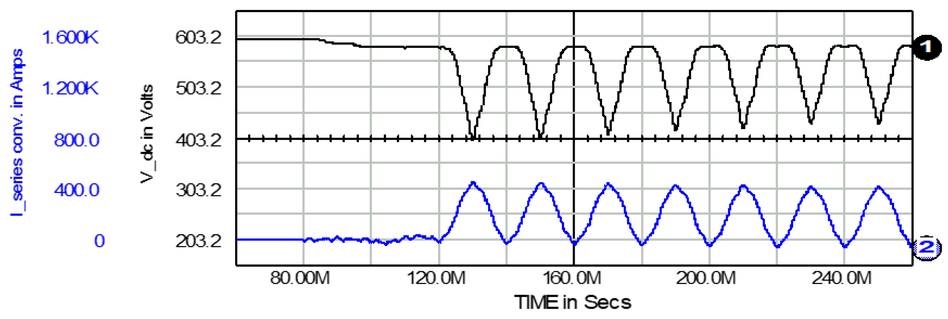
4.1.4. UPQC Operation During Switched Passive/Active Work of DC-Side Load
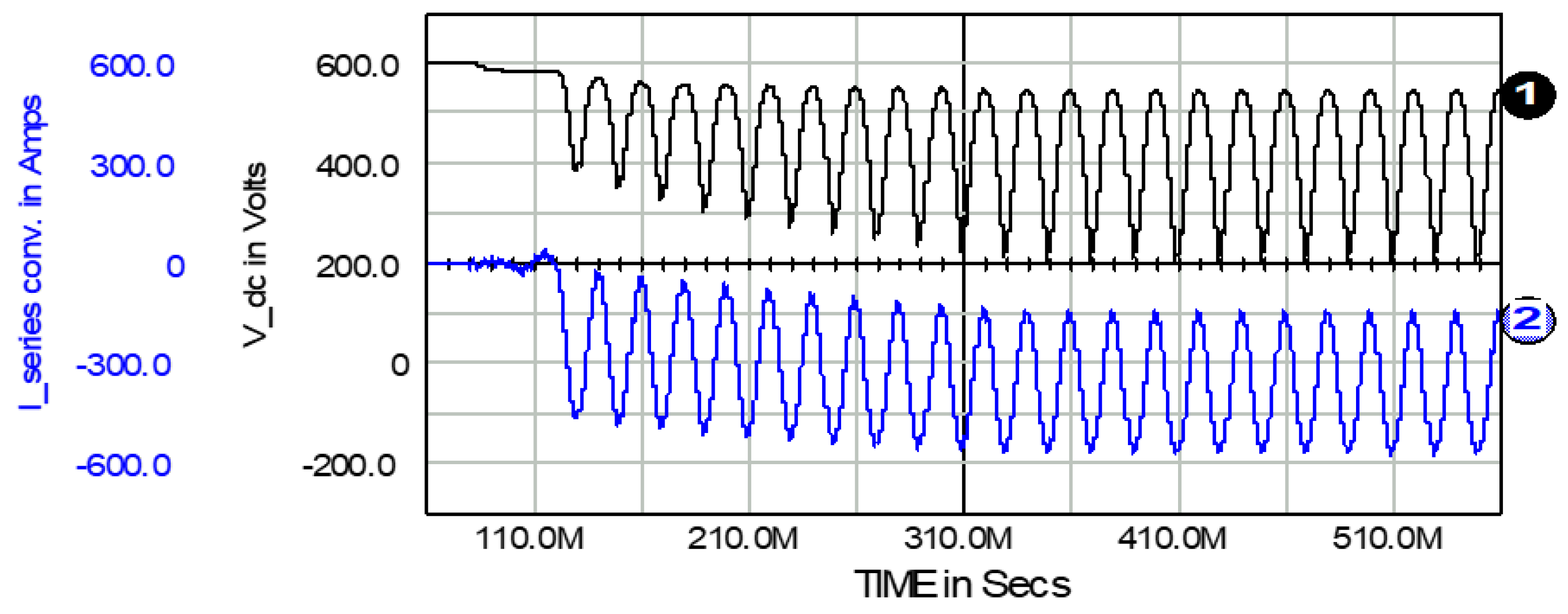
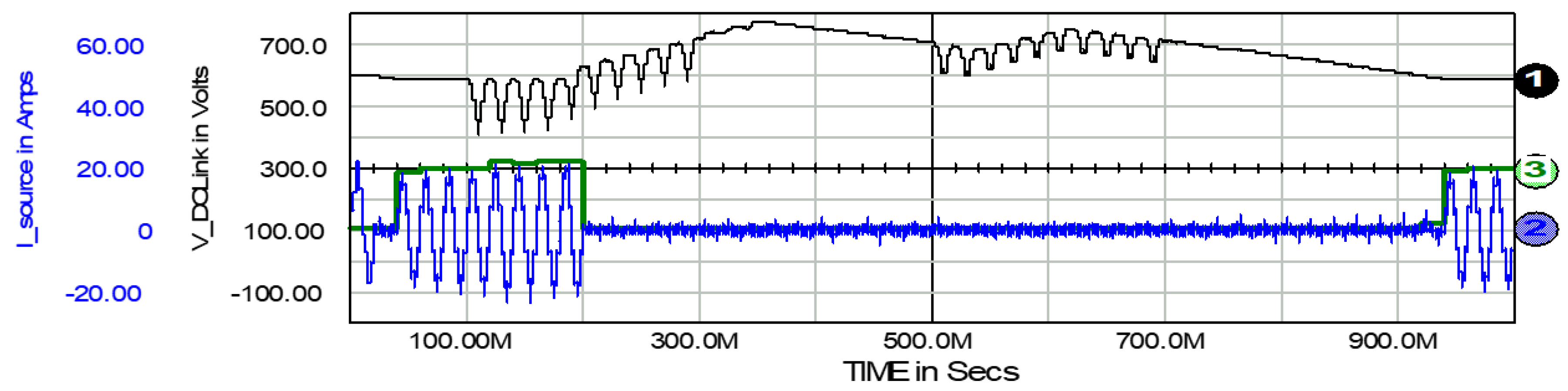
In order to extend the UPQC usefulness a load as well as a source of energy may be connected to the UPQC’s DC-link capacitor. In such a case UPQC can perform some extra tasks. In particular, depending on direction of energy flow, UPQC can act as a high power factor rectifier, which can power DC-side loads with the use of AC-side generated energy, or as an inverter, which can supply AC-side loads with the use of energy generated by DC-side sources. Therefore, UPQC may also serve as an energy bridge and buffer that can control energy flow between all UPQC’s AC-side and DC-side loads and sources. Figure 33 and Figure 34 illustrate such extended mode of UPQC operation.
In Figure 33 UPQC operates in the steady state when a DC-side current of 10 A magnitude begins to charge the DC-link capacitor at the moment t = 60 ms, waveform 1 in Figure 33. Due to the increase in DC-link capacitor voltage, the conductance signal changes both its magnitude and sign to be negative, waveform 3 in Figure 33 and waveform 5 in Figure 34.
As a result energy of this charging DC-side current is transferring to the AC-side network. This energy can power AC-side loads and, concurrently, its surplus may be transmitted upstream to the grid. This to-the-grid energy transferring process starts at t = 80 ms, waveform 4 in Figure 34.
Then, at time instant t = 120 ms, the DC-side current begins to discharge the DC-link capacitor. The conductance signal is recalculated into a new magnitude that depends on sum of AC-side and DC-side active powers. As a result the UPQC, still compensating for voltage and current disturbances, operates concurrently as a high power factor rectifier, i.e., a rectifier with sinusoidal input current, waveform 4 in Figure 34.
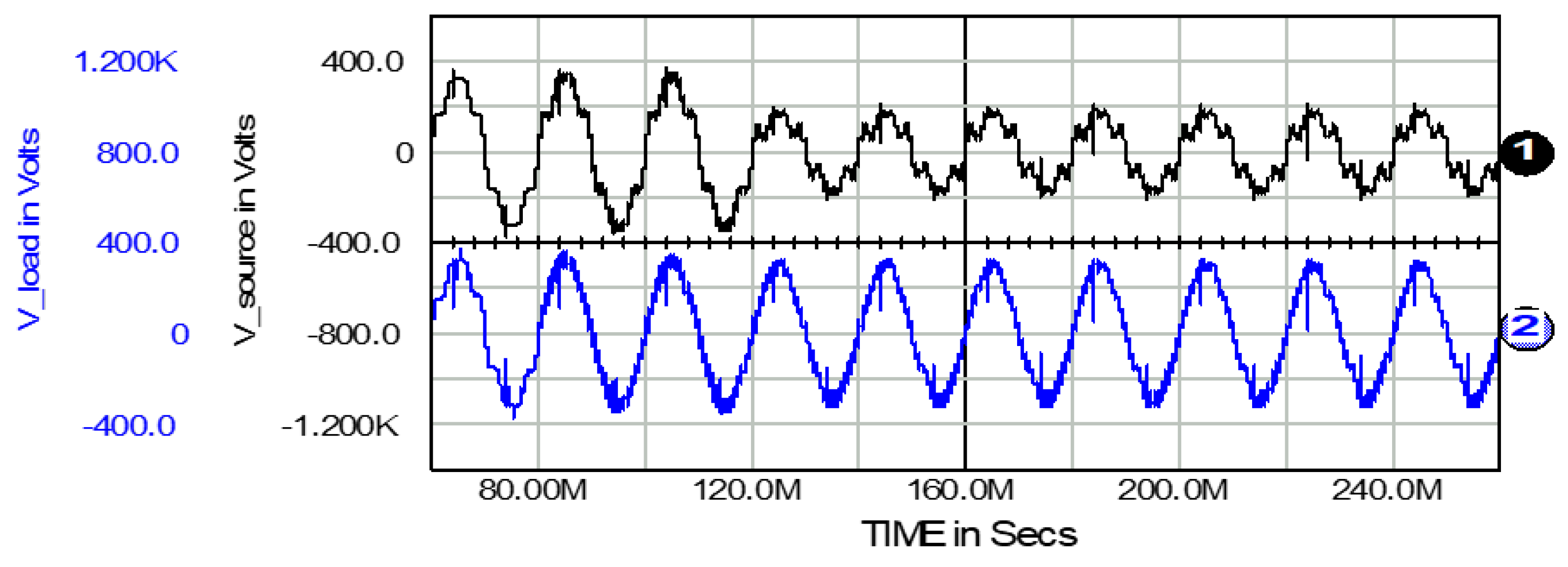
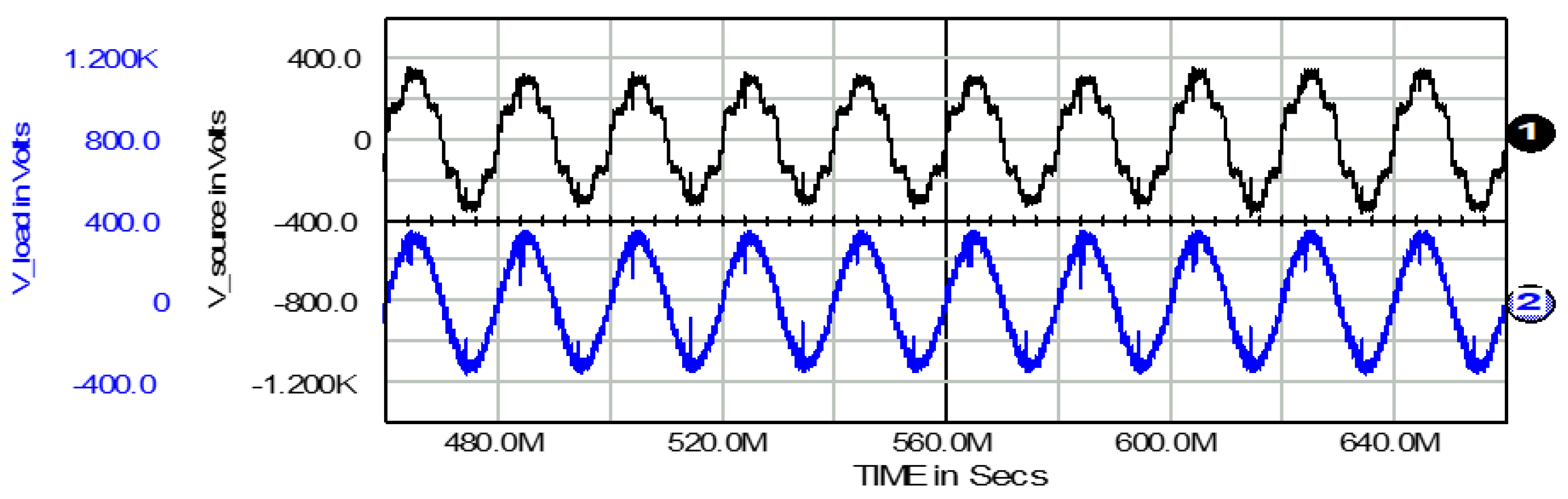
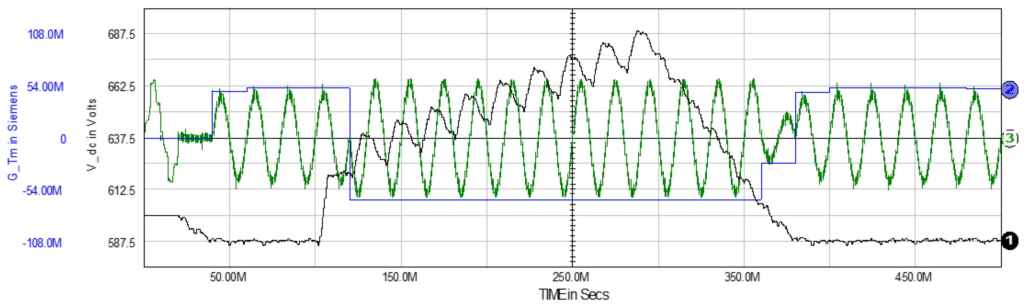
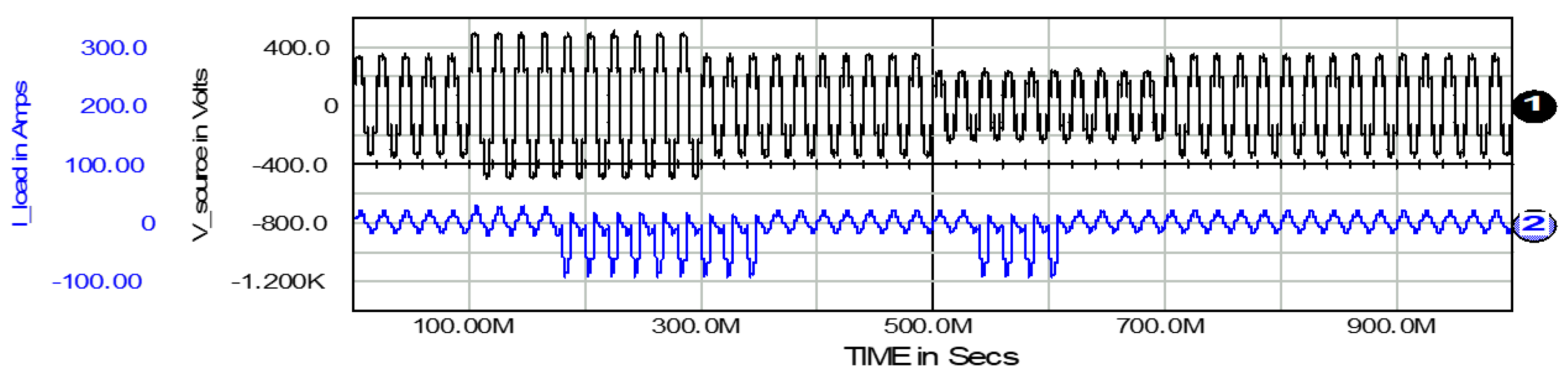
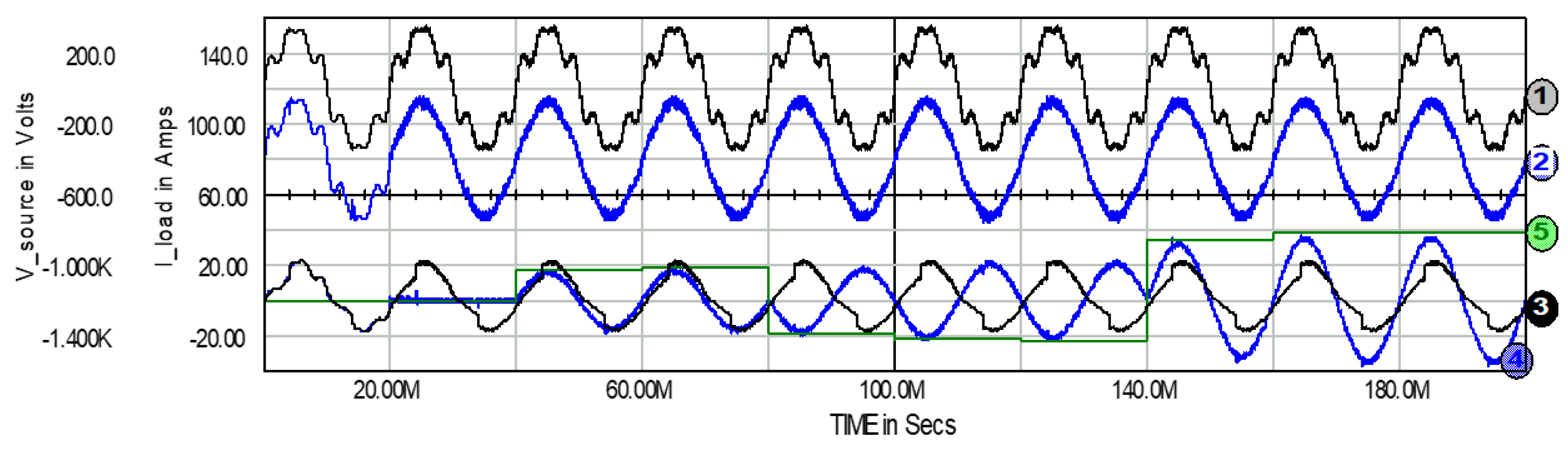
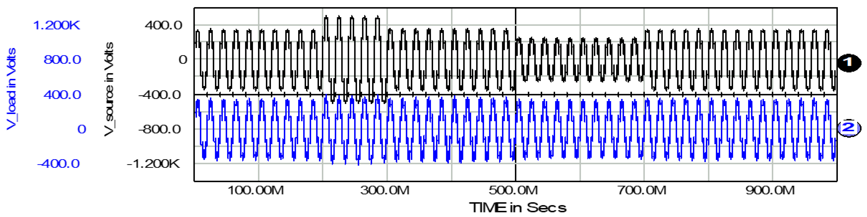
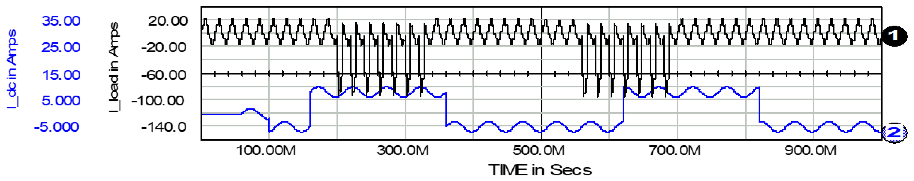
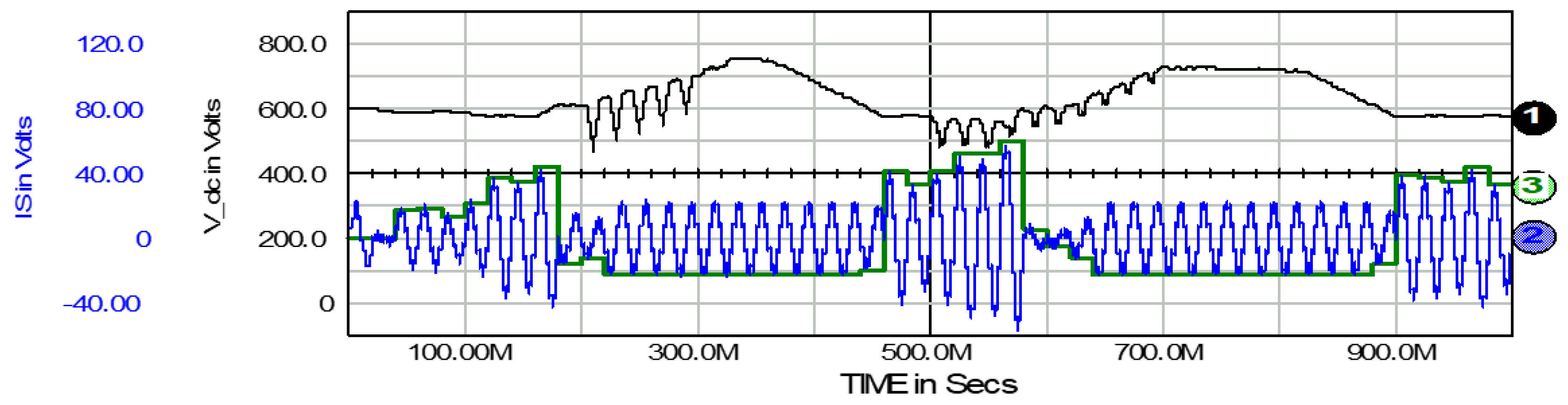
Figure 35, Figure 36, Figure 37, Figure 38 and Figure 39 characterize the UPFC work for when voltage/current runs to be compensated are highly and variously distorted. An additional element, which can operate either as a load or a source of energy and which power can vary in time both in magnitude and in sign, is connected on the DC-link capacitor. Such a network can be considered as generating a kind of worst case of voltage and current runs to be improved. Parameters of these voltage/current runs are specified in the comment that follows Figure 36.
The distorted AC-side source voltage and then the compensated AC-side load voltage are shown in Figure 35. The AC source voltage is distorted by the same higher harmonics and swell/sag disturbances compared to that shown in Figure 23, but this time the whole system is also influenced by energy consumption/generation by the DC-side circuitry. The current run of the DC-side load/source element is shown in Figure 36. Positive polarity of this current means that this element generates energy and vice versa.
DC-link capacitor voltage, AC-side source current and conductance signal (shown as the envelope of source current) are presented in Figure 37. These signals are essential for discussing the UPQC extended operation. In particular, energy balancing between all sources and loads of the network as well as UPQC’s “internal energy effort” in order to compensate for nonactive voltage and current components can be identified when analyzing the waveform of DC-link capacitor voltage. This voltage run contains the in-T-period oscillations that relate to compensation for nonactive components of AC-side current and voltage. In the same time the DC-link capacitor voltage increases or decreases statically, i.e., from Tn period to Tn+1 one, when UPQC balances active powers of all loads and energy sources of the network.
The most critical conditions for UPQC action appear around 200 ms–300 ms and 500 ms–700 ms. They may be treated as a base for a general assessment of UPQC performance.
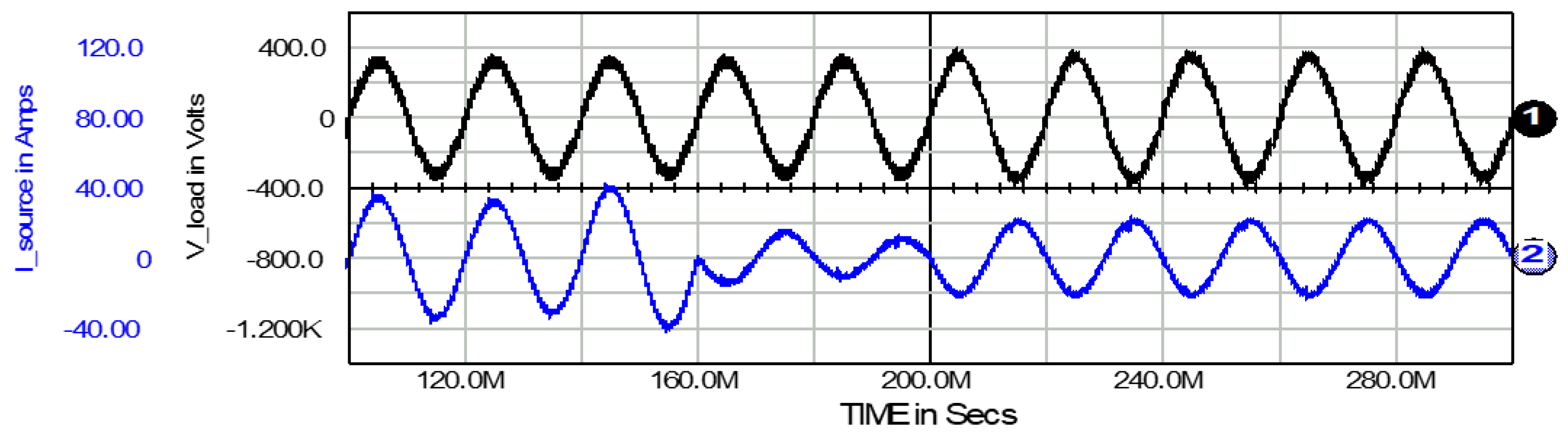
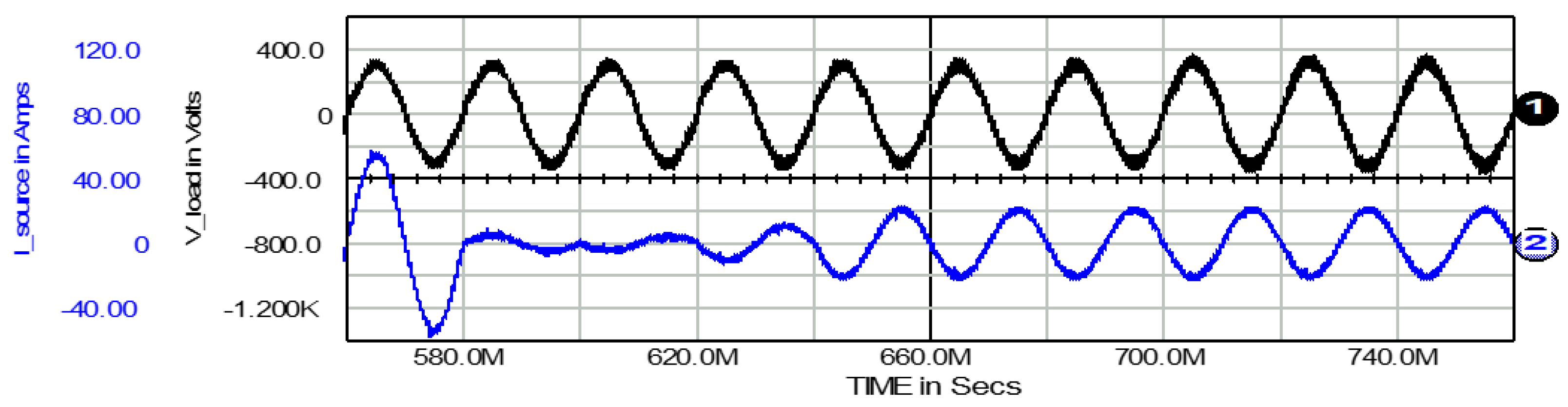
- (a)
- The first critical time period 200 ms–300 ms: There exist a 50% increase in the amplitude of fundamental component of AC source voltage, a large harmonic deformation with heavy DC-component in AC-side load current and successive energy generation/consumption with variable power on UPQC’s DC-side circuitry. The related UPQC’s output runs, i.e., AC-side load voltage and AC-side source current, are shown in Figure 38. For the steady state of the grid waveforms, T period 220 ms–240 ms, parameters of UPQC’s input and output runs are:
- source voltage RMS/THD of 348 V/14.5% have been transformed into load voltage 247 V/3.8%, respectively;
- load current THD of 82.3% and its DC component of magnitude −28.2 A have been transformed into source current THD and DC component of 1.9% and 0.0 A, respectively.
- (b)
- The second critical time period 500 ms–700 ms. There is a 33% decrease in the amplitude source voltage fundamental component, other parameters are the same as in (a). The UPQC output signals are shown in Figure 39. For the steady state of grid runs within this region, T period 660 ms–680 ms, parameters of UPQC’s input and output signals are as follows:
- source voltage RMS of 162 V and THD of 33.2% have been transformed into load voltage RMS and THD of 218 V and 4.6%, respectively;
- load current THD and DC component of 79.5% and −28.5 A has been transformed into source current THD and DC component of 2.6% and 0.1 A, respectively.
It can be stated that in both critical areas of the UPQC operation the disturbed input voltage and current runs have been compensated satisfactory.
5. Conclusions
The paper presents the possibility of compensation for nonactive voltage/current components with the use of compensators that are controlled using a conductance signal. In general, the conductance signal results from the active power of the compensated load. This signal can be calculated based on two variables to be measured:
- (a)
- signal of load power—But obtained indirectly, by measuring energy stored in the reactive elements of the compensator;
- (b)
- signal of supply voltage.
By using the conductance signal as the reference for the compensator action it is possible to omit the technically complicated methods of analysis of voltage/current waveforms by their decomposition into plurality of components. The same idea of avoiding the harmonic analysis is visible here if one compares the considered method to the p-q instantaneous power theory and its use to compensators control. Depending on planned purpose of compensation, such a solution may well be an advantage or a disadvantage.
The conductance signal is obtained based on observation of energy balance in the circuit consisting of the source, the UPQC compensator and the load. Any energy imbalance between the power required by the load and supplied by the source is buffered by the UPQC. In other words the network aims the steady state under control of the UPQC.
Using the conductance signal control method extends the functionality of UPQC. There is the possibility of controlling the flow of energy between all active and passive components of the network. This can help to increase the efficiency of the network.
The use of conductance signal in order to control the UPQC action enables bi-directional energy transmission with unity power factor both from the source to the load and in the opposite direction when the load can also generate energy. Both UPQC’s AC- and DC-side generated or consumed energy may be handled and exchanged in such bi-directional way. This opens the possibility of using UPQC also as a local energy buffering-and-distribution center that can be useful for smart microgrids, increasing their energy efficiency.
Funding
This research received no external funding.
Conflicts of Interest
The author declares no conflict of interest.
References
- Singh, B.; Chandra, A.; Al-Haddad, K. Power Quality: Problems and Mitigation Techniques; John Wiley & Sons: Hoboken, NJ, USA, 2014. [Google Scholar]
- Akagi, H.; Watanabe, E.; Aredes, M. Instantaneous Power Theory and Applications to Power Conditioning; IEEE Press: Piscataway, NJ, USA, 2017. [Google Scholar]
- Khadkikar, V. Enhancing electric power quality using UPQC: A comprehensive overview. IEEE Trans. Power Electron. 2012, 27, 2284–2297. [Google Scholar] [CrossRef]
- Chen, D.; Xiao, L. Novel Fundamental and Harmonics Detection Method Based on State-Space Model for Power Electronics System. IEEE Access 2020, 8, 170002–170012. [Google Scholar] [CrossRef]
- Harirchi, F.; Simoes, M.G. Enhanced instantaneous power theory decomposition for power quality smart converter applications. IEEE Trans. Power Electron. 2018, 33, 9344–9359. [Google Scholar] [CrossRef]
- Pinto, J.O.; Macedo, R.; Monteiro, V.; Barros, L.; Sousa, T.; Alfonso, J. Single-phase shunt active power filter based on a 5-Level converter topology. Energies 2018, 11, 1019. [Google Scholar] [CrossRef] [Green Version]
- Fryze, S. Wirk-, Blind-, und Scheinleistung in Elektrischen Stromkreisen mit nichtsinusformigem Verlauf von Strom und Spannung. Elektrotechnische Z. 1932, 25, 33. [Google Scholar]
- Szromba, A. Conductance-controlled global-compensation-type shunt active power filter. Arch. Electr. Eng. 2015, 64, 259–275. [Google Scholar] [CrossRef]
- Szromba, A.; Mysiński, W. Voltage-source-based conductance-signal controlled shunt active power filter. In Proceedings of the 2017 European Conference on Power Electronics an Applications, Warsaw, Poland, 11–14 September 2017. [Google Scholar]
- Orts-Grau, S.; Gimeno-Sales, F.J.; Segui-Chilet, S.; Abellen-Garcia, A.; Alcaniz-Fillol, M.; Masot-Periz, R. Selective compensation in four-wire electric systems based on a new equivalent conductance approach. IEEE Trans. Ind. Electron. 2009, 56, 2862–2874. [Google Scholar] [CrossRef]
- Montero, M.I.; Cadaval, E.R.; Gonzalez, F.B. Comparison of control strategies for shunt active power filters in three-phase four-wire systems. IEEE Trans. Power Electron. 2007, 22, 229–236. [Google Scholar] [CrossRef]
- Moreno, V.; Pigazo, A. Modified FBD method in active power filters to minimize the line current harmonics. IEEE Trans. Power Deliv. 2006, 22, 735–736. [Google Scholar] [CrossRef]
- Hafezi, H.; D’Antona, G.; Dede, A.; Giustina, D.D.; Faranda, R.; Massa, G. Power quality conditioning in LV distribution networks: Results by field demonstration. IEEE Trans. Smart Grid 2017, 8, 418–427. [Google Scholar] [CrossRef]
- Panda, A.K.; Patnaik, N. Management of reactive power sharing and power quality improvement with SRF-PAC based UPQC under unbalanced source voltage condition. Int. J. Electr. Power Energy Syst. 2017, 84, 182–194. [Google Scholar] [CrossRef]
- Ambati, B.B.; Khadkikar, V. Optimal sizing of UPQC considering VA loading and maximum utilization of power-electronics converters. IEEE Trans. Power Deliv. 2014, 29, 1490–1498. [Google Scholar] [CrossRef]
- Ye, J.; Gooi, H.B.; Wu, F. Optimization of the size of UPQC system based on data-driven control design. IEEE Trans. Smart Grid 2018, 9, 2999–3008. [Google Scholar] [CrossRef]
- Moghbel, M.; Masoum, M.A.; Fereidouni, A.; Deilami, S. Optimal sizing, siting and operation of custom power devices with STATCOM and APLC functions for real-time reactive power and network voltage quality control of smart grid. IEEE Trans. Smart Grid 2018, 9, 5564–5575. [Google Scholar] [CrossRef]
- Campanhol, L.B.; da Silva, S.A.; de Oliveira, A.A.; Bacon, V.D. Power flow and stability analyses of a multifunctional distributed generation system integrating a photovoltaic system with Unified Power Quality Conditioner. IEEE Trans. Power Electron. 2019, 34, 6241–6256. [Google Scholar] [CrossRef]
- Kaur, A.; Kaushal, J.; Basak, P. A review on microgrid central controller. Renew. Sustain. Energy Rev. 2016, 55, 338–345. [Google Scholar] [CrossRef]
- Asiminoaei, L.; Blaabjerg, F.; Hansen, S. Detection is key. Harmonic detection methods for active power filter applications. IEEE Ind. Appl. Mag. 2007, 13, 22–33. [Google Scholar] [CrossRef]
- Tareen, W.; Mekhilef, S.; Seyedmahmoudian, M.; Horan, B. Active power filter (APF) for mitigation of power quality issues in grid integration of wind and photovoltaic energy conversion system. Renew. Sustain. Energy Rev. 2017, 70, 635–655. [Google Scholar] [CrossRef]
- Farhadi-Kangarlu, M.; Babaei, E.; Blaabjerg, F. A comprehensive review of dynamic voltage restorers. Electr. Power Energy Syst. 2017, 92, 136–155. [Google Scholar] [CrossRef]
Figure 1.
UPQC power circuitry diagram and scheme of obtaining conductance signal on the base of DC-link capacitor voltage vdc, according to Equation (6). The S/H block is an sample-and-hold module that is synchronized with source voltage waveform using sync block.
Figure 1.
UPQC power circuitry diagram and scheme of obtaining conductance signal on the base of DC-link capacitor voltage vdc, according to Equation (6). The S/H block is an sample-and-hold module that is synchronized with source voltage waveform using sync block.

Figure 2.
Shunt converter turning on. Source voltage: run 1, source current: 2, conductance signal: 3. Y scale for conductance signal is 45 mS/div.
Figure 2.
Shunt converter turning on. Source voltage: run 1, source current: 2, conductance signal: 3. Y scale for conductance signal is 45 mS/div.

Figure 3.
Shunt converter turning on process. DC-link capacitor voltage: waveform 1, and load equivalent conductance signal: waveform 2.
Figure 3.
Shunt converter turning on process. DC-link capacitor voltage: waveform 1, and load equivalent conductance signal: waveform 2.

Figure 4.
Series converter turning on. Load voltage: waveform 1, and DC-link capacitor voltage: waveform 2.
Figure 4.
Series converter turning on. Load voltage: waveform 1, and DC-link capacitor voltage: waveform 2.

Figure 5.
Series converter turning on process. Source current: waveform 1, and conductance signal: waveform 2.
Figure 5.
Series converter turning on process. Source current: waveform 1, and conductance signal: waveform 2.

Figure 6.
Load turning off process. Load voltage: waveform 1, and load current: waveform 2.

Figure 7.
Load turning off process. Load voltage: waveform 1, and source current: waveform 2.

Figure 8.
Load turning off process. DC-link capacitor voltage: waveform 1, and load conductance signal: waveform 2.
Figure 8.
Load turning off process. DC-link capacitor voltage: waveform 1, and load conductance signal: waveform 2.

Figure 9.
Source voltage swell compensation. Source voltage: waveform 1, and load voltage: waveform 2.
Figure 9.
Source voltage swell compensation. Source voltage: waveform 1, and load voltage: waveform 2.

Figure 10.
Source voltage swell. Load current, source current and conductance signal: waveforms 1, 2 and 3.
Figure 10.
Source voltage swell. Load current, source current and conductance signal: waveforms 1, 2 and 3.

Figure 11.
Source voltage swell. DC-link capacitor voltage and series converter current: waveforms 1 and 2.
Figure 11.
Source voltage swell. DC-link capacitor voltage and series converter current: waveforms 1 and 2.

Figure 12.
Source voltage sag compensation. Source voltage: waveform 1 and load voltage: waveform 2.
Figure 12.
Source voltage sag compensation. Source voltage: waveform 1 and load voltage: waveform 2.

Figure 13.
Source voltage sag compensation. Source current: waveform 1, load current: waveform 2, and conductance signal: waveform 3.
Figure 13.
Source voltage sag compensation. Source current: waveform 1, load current: waveform 2, and conductance signal: waveform 3.

Figure 14.
Source voltage sag compensation. DC-link capacitor voltage and load series converter current: waveform 1 and 2, respectively.
Figure 14.
Source voltage sag compensation. DC-link capacitor voltage and load series converter current: waveform 1 and 2, respectively.

Figure 15.
Source voltage flicker compensation. DC-link capacitor voltage for Tst = T and for Tst = 3T: waveforms 2 and 4, respectively, and conductance signal for Tst = T and for Tst = 3T: waveforms 1 and 3, respectively.
Figure 15.
Source voltage flicker compensation. DC-link capacitor voltage for Tst = T and for Tst = 3T: waveforms 2 and 4, respectively, and conductance signal for Tst = T and for Tst = 3T: waveforms 1 and 3, respectively.

Figure 16.
Source voltage flicker compensation. Source voltage: waveform 1, and harmonics-compensated and amplitude-levelled load voltage: waveform 2.
Figure 16.
Source voltage flicker compensation. Source voltage: waveform 1, and harmonics-compensated and amplitude-levelled load voltage: waveform 2.

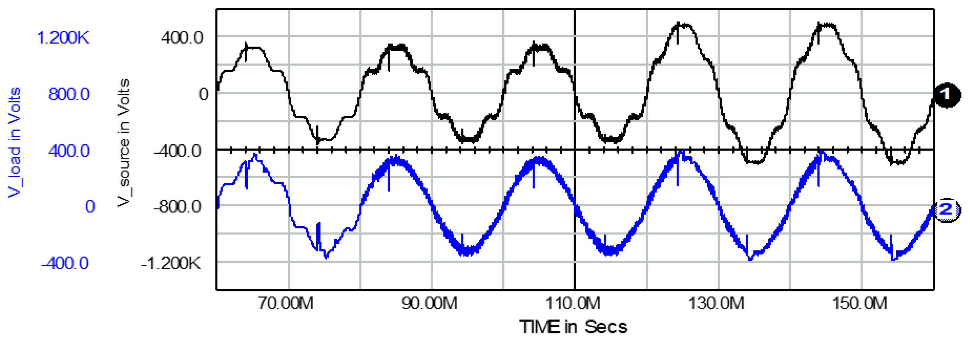
Figure 17.
Source voltage: waveform 1, load voltage: waveform 2 and load current: waveform 3. Whole network action, general view.
Figure 17.
Source voltage: waveform 1, load voltage: waveform 2 and load current: waveform 3. Whole network action, general view.

Figure 18.
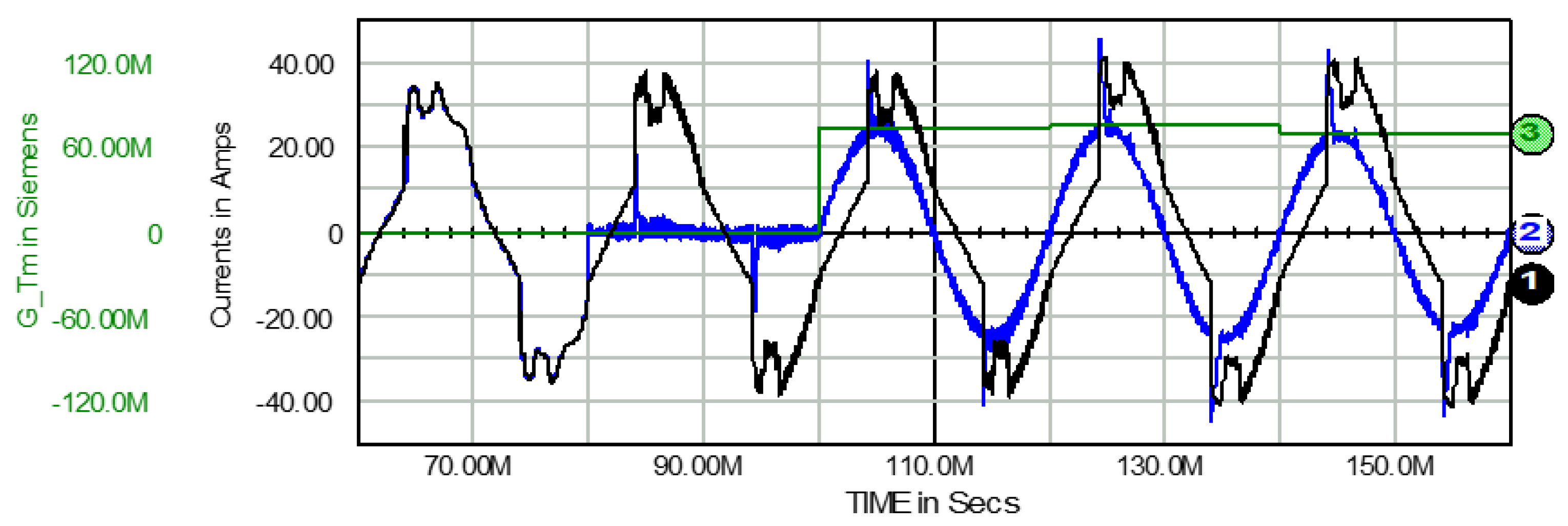
DC-link capacitor voltage: waveform 1, conductance signal: waveform 2 and source current: waveform 3 with Y scale of 54 mS/div. Whole network action, case 4.1 (a).
Figure 18.
DC-link capacitor voltage: waveform 1, conductance signal: waveform 2 and source current: waveform 3 with Y scale of 54 mS/div. Whole network action, case 4.1 (a).

Figure 19.
DC-link capacitor voltage: waveform 1, conductance signal: waveform 2 and source current: waveform 3 with Y scale of 10 A/div. Whole network action, case 4.1 (b).
Figure 19.
DC-link capacitor voltage: waveform 1, conductance signal: waveform 2 and source current: waveform 3 with Y scale of 10 A/div. Whole network action, case 4.1 (b).

Figure 20.
Load voltage: waveform 1, load current: waveform 2 and source current: waveform 3.

Figure 21.
Load current: waveform 1 and source current: waveform 2.

Figure 22.
Load current: waveform 1 and source current: waveform 2.

Figure 23.
Source voltage: waveform 1 and load current: waveform 2.

Figure 24.
DC-link capacitor voltage: waveform 1, source current: 2 and conductance signal: 3 with Y scale of 27 mS/div.
Figure 24.
DC-link capacitor voltage: waveform 1, source current: 2 and conductance signal: 3 with Y scale of 27 mS/div.

Figure 25.
Source and load voltages: waveform 1 and 2. Theirs RMS and THD parameters are 348 V and 14.7%, and then 268 V and 7.7%, respectively.
Figure 25.
Source and load voltages: waveform 1 and 2. Theirs RMS and THD parameters are 348 V and 14.7%, and then 268 V and 7.7%, respectively.

Figure 26.
Source and load voltages: waveform 1 and 2. Theirs RMS and THD parameters are 162 V and 32.7%, and then 219 V and 4.1%, respectively.
Figure 26.
Source and load voltages: waveform 1 and 2. Theirs RMS and THD parameters are 162 V and 32.7%, and then 219 V and 4.1%, respectively.

Figure 27.
Source and load voltages: waveform 1 and 2. Theirs RMS and THD parameters are 235 V and 21.4%, and then 231 V and 4.3%, respectively.
Figure 27.
Source and load voltages: waveform 1 and 2. Theirs RMS and THD parameters are 235 V and 21.4%, and then 231 V and 4.3%, respectively.

Figure 28.
Source and load voltages: waveform 1 and 2. Theirs RMS and THD parameters are 235 V and 21.7%, and then 231 V and 4.7%, respectively.
Figure 28.
Source and load voltages: waveform 1 and 2. Theirs RMS and THD parameters are 235 V and 21.7%, and then 231 V and 4.7%, respectively.

Figure 29.
Source and load voltages: waveform 1 and 2. Theirs RMS and THD parameters are 162 V and 32.6%, and then 219 V and 4.2%, respectively.
Figure 29.
Source and load voltages: waveform 1 and 2. Theirs RMS and THD parameters are 162 V and 32.6%, and then 219 V and 4.2%, respectively.

Figure 30.
Source voltage with spike distortion: waveform 1 and DC-link capacitor voltage: waveform 2.
Figure 30.
Source voltage with spike distortion: waveform 1 and DC-link capacitor voltage: waveform 2.

Figure 31.
Source voltage: waveform 1 and load voltage: waveform 2.

Figure 32.
Conductance signal: waveform 1 and source current: waveform 2.

Figure 33.
DC-side load current: waveform 1, DC-link capacitor voltage: waveform 2 and conductance signal: waveform 3 (Y scale for this signal is 25 mS/div).
Figure 33.
DC-side load current: waveform 1, DC-link capacitor voltage: waveform 2 and conductance signal: waveform 3 (Y scale for this signal is 25 mS/div).

Figure 34.
AC-side source voltage: waveform 1, AC-side load voltage: waveform 2, AC-side load current: waveform 3, AC-side source current: waveform 4 and conductance signal: waveform 5, where Y scale for the conductance signal is 57 mS/div.
Figure 34.
AC-side source voltage: waveform 1, AC-side load voltage: waveform 2, AC-side load current: waveform 3, AC-side source current: waveform 4 and conductance signal: waveform 5, where Y scale for the conductance signal is 57 mS/div.

Figure 35.
Global view on AC-side source voltage: waveform 1 and on AC-side load voltage: waveform 2.
Figure 35.
Global view on AC-side source voltage: waveform 1 and on AC-side load voltage: waveform 2.

Figure 36.
Global view on AC-side load current: waveform 1 and on DC-side load current: waveform 2.

Figure 37.
Global view on DC-link capacitor voltage: waveform 1, AC-side source current: waveform 2 and conductance signal: waveform 3 with Y scale of 56 mS/div.
Figure 37.
Global view on DC-link capacitor voltage: waveform 1, AC-side source current: waveform 2 and conductance signal: waveform 3 with Y scale of 56 mS/div.

Figure 38.
Critical time period 100 ms–300 ms. AC-load voltage: waveform 1 and AC-source current: waveform 2.
Figure 38.
Critical time period 100 ms–300 ms. AC-load voltage: waveform 1 and AC-source current: waveform 2.

Figure 39.
Critical time period 560 ms–760 ms. AC-load voltage: waveform 1 and AC-source current: waveform 2.
Figure 39.
Critical time period 560 ms–760 ms. AC-load voltage: waveform 1 and AC-source current: waveform 2.


Table 1.
Compensated load basic electrical parameters just before (for 380 ms–400 ms) and after (for 400 ms–460 ms) the instant (at 400 ms) of turning the shunt converter on.
Table 1.
Compensated load basic electrical parameters just before (for 380 ms–400 ms) and after (for 400 ms–460 ms) the instant (at 400 ms) of turning the shunt converter on.
| Time (ms) | 380–400 | 400–420 | 420–440 | 440–460 |
|---|---|---|---|---|
| Parameter | ||||
| VLoad (V) | 229 | 234 | 234 | 234 |
| ILoad (A) | 15.6 | 16.6 | 17.0 | 17.0 |
| SLoad (VA) | 3572 | 3884 | 3978 | 3978 |
| PLoad (W) | 2439 | 2743 | 2885 | 2879 |
| PFLoad | 0.68 | 0.71 | 0.73 | 0.73 |
| WLoad (J) | 48.8 | 54.9 | 57.7 | 57.6 |
| GLoad (mS) | 46.6 | 50.1 | 52.7 | 52.6 |
VLoad and ILoad are voltage and current rms on load terminals, SLoad and PLoad are load apparent and active powers, PFLoad is load power factor, WLoad is energy consumed by load, GLoad is load equivalent conductance equal to PLoad/(VLoad)2.
Table 2.
UPQC-and-load subcircuit basic electrical parameters before (380 ms–400 ms) and after (400 ms–460 ms) the instant (at 400 ms) of turning the shunt converter on.
Table 2.
UPQC-and-load subcircuit basic electrical parameters before (380 ms–400 ms) and after (400 ms–460 ms) the instant (at 400 ms) of turning the shunt converter on.
| Time (ms) | 380–400 | 400–420 | 420–440 | 440–460 |
|---|---|---|---|---|
| Parameter | ||||
| VSource (V) | 232 | 232 | 232 | 232 |
| ISource (A) | 15.5 | 2.8 | 12.1 | 12.9 |
| ISource THD (%) | 59 | 146 | 17 | 14 |
| SUPQC+Load (VA) | 596 | 650 | 2807 | 2993 |
| PUPQC+Load (W) | 449 | 277 | 2717 | 2899 |
| PFUPQC+Load | 0.68 | 0.42 | 0.97 | 0.97 |
| WUPQC+Load (J) | 49.0 | 5.5 | 54.3 | 58.0 |
| ∆WDCCap (J) | 0.0 | −49.5 | −4.2 | 0.0 |
| GSignal (mS) | 1.2 | 1.2 | 42.3 | 59.0 |
VSource and ISource are voltage and current rms on UPQC terminals, ISource THD is source current THD factor, SUPQC+Load and PUPQC+Load are UPQC-and-load apparent and active powers seen on UPQC terminals, PFUPQC+Load is UPQC-and-load subcircuit power factor, WUPQC+Load is energy delivered to UPQC-and-load subcircuit from source, ∆WDCCap is change of energy stored in DC-link capacitor, GSignal is signal of load equivalent conductance calculated accordingly to Equation (5).
Table 3.
Basic parameters describing load action before (780 ms–800 ms) and after (800 ms–860 ms) the instant (800 ms) of turning the series converter on.
Table 3.
Basic parameters describing load action before (780 ms–800 ms) and after (800 ms–860 ms) the instant (800 ms) of turning the series converter on.
| Time (ms) | 780–800 | 800–820 | 820–840 | 840–860 |
|---|---|---|---|---|
| Parameter | ||||
| VLoad (V) | 234 | 229 | 229 | 229 |
| VLoad THD (%) | 15 | 3.3 | 3.1 | 3.5 |
| ILoad (A) | 16.9 | 16.1 | 16.1 | 16.0 |
| SLoad (VA) | 3955 | 3687 | 3686 | 3664 |
| PLoad (W) | 2873 | 2589 | 2608 | 2563 |
| PFLoad | 0.73 | 0.86 | 0.71 | 0.70 |
| WLoad (J) | 57.5 | 51.8 | 52.2 | 51.3 |
| GLoad (mS) | 52.4 | 49.5 | 49.9 | 49.0 |
VLoad THD [%] is load voltage THD factor and other parameters are defined as for Table 1.
Table 4.
Basic parameters describing load action before, (780 ms–800 ms) and after (800 ms–860 ms) the instant (800 ms) of turning the series converter on. All parameters are defined as for Table 2.
Table 4.
Basic parameters describing load action before, (780 ms–800 ms) and after (800 ms–860 ms) the instant (800 ms) of turning the series converter on. All parameters are defined as for Table 2.
| Time (ms) | 780–800 | 800–820 | 820–840 | 840–860 |
|---|---|---|---|---|
| Parameter | ||||
| VSource (V) | 232 | 232 | 232 | 232 |
| ISource (A) | 12.9 | 13.1 | 12.0 | 12.1 |
| ISource THD (%) | 14 | 13 | 14 | 14 |
| SUPQC+Load (VA) | 2993 | 3039 | 2784 | 2807 |
| PUPQC+Load (W) | 2908 | 2919 | 2659 | 2692 |
| PFUPQC+Load | 0.97 | 0.96 | 0.96 | 0.96 |
| WUPQC+Load (J) | 58.2 | 58.4 | 53.2 | 53.8 |
| ∆WDCCap (J) | 0.5 | 5.2 | −0.9 | 1.9 |
| GSignal (mS) | 51.0 | 50.8 | 45.8 | 46.3 |
Table 5.
Basic parameters characterizing load work before and during source voltage swell. The parameter definitions are the same as for Table 3.
Table 5.
Basic parameters characterizing load work before and during source voltage swell. The parameter definitions are the same as for Table 3.
| Time (ms) | 0–80 | 80–100 | 100–120 | 120–140 | 180–200 | 240–260 |
|---|---|---|---|---|---|---|
| Parameter | ||||||
| VLoad (V) | 225 | 229 | 228 | 247 | 248 | 247 |
| ILoad (A) | 22.3 | 22.4 | 22.3 | 24.6 | 24.6 | 24.8 |
| SLoad (VA) | 5018 | 5130 | 5084 | 6076 | 6101 | 6126 |
| PLoad (W) | 4203 | 4278 | 4241 | 5145 | 5147 | 5214 |
| PFLoad | 0.84 | 0.83 | 0.83 | 0.85 | 0.84 | 0.85 |
| WLoad (J) | 84.0 | 85.6 | 84.8 | 102.9 | 102.9 | 104.3 |
| GLoad (mS) | 83.0 | 81.6 | 81.6 | 84.3 | 83.7 | 85.5 |
Table 6.
Basic parameters characterizing UPQC-and-load subcircuit operation for the voltage swell. The parameter describing is the same as for Table 2.
Table 6.
Basic parameters characterizing UPQC-and-load subcircuit operation for the voltage swell. The parameter describing is the same as for Table 2.
| Time (ms) | 60–80 | 80–100 | 100–120 | 120–140 | 180–200 | 240–260 |
|---|---|---|---|---|---|---|
| Parameter | ||||||
| VSource (V) | 231 | 232 | 232 | 346 | 346 | 346 |
| ISource (A) | 22.2 | 2.6 | 18.2 | 19.0 | 17.7 | 17.7 |
| SUPQC+Load (VA) | 5128 | 603 | 4222 | 6574 | 6124 | 6124 |
| PUPQC+Load (W) | 4210 | 254 | 4146 | 6458 | 6014 | 6009 |
| PFUPQC+Load | 0.82 | 0.42 | 0.98 | 0.98 | 0.98 | 0.98 |
| WUPQC+Load (J) | 84.2 | 5.1 | 82.9 | 129.2 | 120.3 | 120.2 |
| ∆WDCCap (J) | −1.0 | −81.8 | −2.8 | 7.0 | −0.5 | 0.0 |
| GSignal (mS) | 0.2 | 0.3 | 74.4 | 76.8 | 71.1 | 71.4 |
Table 7.
Basic parameters characterizing load work before and during source voltage sag. The parameter describing is the same as for Table 3.
Table 7.
Basic parameters characterizing load work before and during source voltage sag. The parameter describing is the same as for Table 3.
| Time (ms) | 60–80 | 80–100 | 100–120 | 120–140 | 200–220 | 380–400 |
|---|---|---|---|---|---|---|
| Parameter | ||||||
| VLoad (V) | 225 | 229 | 228 | 214 | 209 | 208 |
| ILoad (A) | 22.3 | 22.4 | 22.3 | 20.9 | 20.7 | 20.2 |
| SLoad (VA) | 5018 | 5130 | 5084 | 4473 | 4326 | 4121 |
| PLoad (W) | 4203 | 4278 | 4241 | 3735 | 3653 | 3487 |
| PFLoad | 0.84 | 0.83 | 0.83 | 0.84 | 0.84 | 0.85 |
| WLoad (J) | 84.1 | 85.6 | 84.8 | 74.7 | 73.1 | 69.7 |
| GLoad (mS) | 83.0 | 81.6 | 81.6 | 81.6 | 83.6 | 83.4 |
Table 8.
Basic parameters describing UPQC-and-load subcircuit action before and during the source voltage sag. The parameters shown were defined in Table 2.
Table 8.
Basic parameters describing UPQC-and-load subcircuit action before and during the source voltage sag. The parameters shown were defined in Table 2.
| Time (ms) | 60–80 | 80–100 | 100–120 | 120–140 | 140–160 | 200–220 | 280–300 | 380–400 |
|---|---|---|---|---|---|---|---|---|
| Parameter | ||||||||
| VSource (V) | 231 | 232 | 232 | 120 | 120 | 120 | 120 | 120 |
| ISource (A) | 22.2 | 2.6 | 18.2 | 18.1 | 30.3 | 44.7 | 46.5 | 46.6 |
| SUPQC+Load (VA) | 5128 | 603 | 4222 | 2172 | 3636 | 5364 | 5580 | 5592 |
| PUPQC+Load (W) | 4210 | 254 | 4146 | 2086 | 3492 | 5123 | 5364 | 5369 |
| PFUPQC+Load | 0.82 | 0.42 | 0.98 | 0.96 | 0.96 | 0.96 | 0.96 | 0.96 |
| WUPQC+Load (J) | 84.2 | 5.1 | 82.9 | 41.7 | 69.8 | 102.5 | 107.3 | 107.4 |
| ∆WDCCap (J) | −0.48 | −82.8 | −2.3 | −57.6 | −33.0 | −7.1 | −10.5 | −0.4 |
| GSignal (mS) | 0.2 | 0.3 | 74.4 | 76.8 | 129.6 | 192.6 | 200.0 | 200.0 |
Publisher’s Note: MDPI stays neutral with regard to jurisdictional claims in published maps and institutional affiliations. |
© 2020 by the author. Licensee MDPI, Basel, Switzerland. This article is an open access article distributed under the terms and conditions of the Creative Commons Attribution (CC BY) license (http://creativecommons.org/licenses/by/4.0/).
Share and Cite
MDPI and ACS Style
Szromba, A. The Unified Power Quality Conditioner Control Method Based on the Equivalent Conductance Signals of the Compensated Load. Energies 2020, 13, 6298. https://doi.org/10.3390/en13236298
AMA Style
Szromba A. The Unified Power Quality Conditioner Control Method Based on the Equivalent Conductance Signals of the Compensated Load. Energies. 2020; 13(23):6298. https://doi.org/10.3390/en13236298
Chicago/Turabian StyleSzromba, Andrzej. 2020. "The Unified Power Quality Conditioner Control Method Based on the Equivalent Conductance Signals of the Compensated Load" Energies 13, no. 23: 6298. https://doi.org/10.3390/en13236298
Note that from the first issue of 2016, this journal uses article numbers instead of page numbers. See further details here.