Optimal Combination Design of a Light Emitting Diode Matrix Applicable to a Single-Stage Flyback Driver


1
Leadtrend Technology Corporation, No.1, Taiyuan 2nd St., Zhubei City 302, Hsinchu County, Taiwan
2
Department of Electrical Engineering, National Taiwan University of Science and Technology, No.43, Section 4, Keelung Road, Da’an District, Taipei City 106, Taiwan
*
Author to whom correspondence should be addressed.
Energies 2020, 13(19), 5209; https://doi.org/10.3390/en13195209
Submission received: 13 September 2020
/
Revised: 30 September 2020
/
Accepted: 2 October 2020
/
Published: 6 October 2020
(This article belongs to the Special Issue Advanced Perspectives for Modeling, Simulation and Control of Power Electronic Systems)
Abstract
:The present study analyzed light emitting diodes (LEDs) as an output load and used a Taylor series to describe the characteristic curve based on the exponential characteristic of voltage and current. A prototype circuit of a flyback LED driver system was established to verify whether the theory is consistent with actual results. This study focused on the exponential relationship of LED voltage and current. Conventional simulations usually used linear models to present LED loads. However, the linear model resulted in considerable error between simulation and actual characteristics. Therefore, this study employed a Taylor series to describe the nonlinear characteristic of an LED load. Through precise calculations with Mathcad computation software, the error was effectively reduced. Moreover, the process clarified the influence of temperature on LEDs, which benefited the characteristic analysis of the entire system. Finally, a realized circuit of 120 W flyback LED drivers was established for conducting theory verification, including theoretic analysis and evaluation of the system design process of the flyback converter. The circuit simulation software SIMPLIS was used to demonstrate the system model, which enabled quick understanding of the system framework established in this study. Regarding LEDs, a commercially available aluminum luminaire was used as the output load. The measured results of the actual circuit and the simulation results were remarkably consistent. For the same system at the same temperature, the error between the simulation and actual results was less than 3%, which proved the reliability of the Taylor series simulation.
1. Introduction
Continual technological developments have improved the human living environment and the convenience of performing everyday activities. However, technological developments have resulted in substantial energy consumption. In recent years, because of problems such as the progression of global warming and energy shortages, people have become increasingly aware of the importance of environmental protection. Therefore, the demands for energy conservation and highly efficient products have increased. Light emitting diode (LED) technology, which has been undergoing development since 1962 [1], has reached a certain level of maturity. Because of their numerous merits and unique features, LEDs have gradually replaced conventional light sources and become the primary light source of this era.
The fluorescent tubes used in fluorescent lamps have an unstable and flickering lighting source, which may cause danger in certain working environments [2,3]. Such unstable light sources cause fatigue for human eyes. Moreover, the mercury contained in fluorescent tubes is harmful to the human body and the environment. In addition, conventional incandescent light bulbs and halogen lamps feature short life expectancy, low efficiency, high power consumption, and high levels of heat generation and thus may be considered to incur excessive energy consumption [4,5].
Technological developments have led to changes in the lighting source, luminaire, control, and design of lighting products that have greatly improved their efficiency. Additionally, the establishment of energy-saving indices and government policies has created further room for improvement in terms of energy-saving characteristics, particularly regarding LED application. The energy consumption of luminescence in LED luminaire systems is remarkably lower than that of conventional light sources such as incandescent light bulbs and fluorescent lamps. The luminescence efficiency of regular high-brightness LED luminaires corresponds to 50% less energy consumption than fluorescent lamps and 85% less than that of incandescent light bulbs [6]. Therefore, adopting energy-saving illumination products to replace conventional ones can achieve optimal energy-saving outcomes and the ultimate goal of energy conservation.
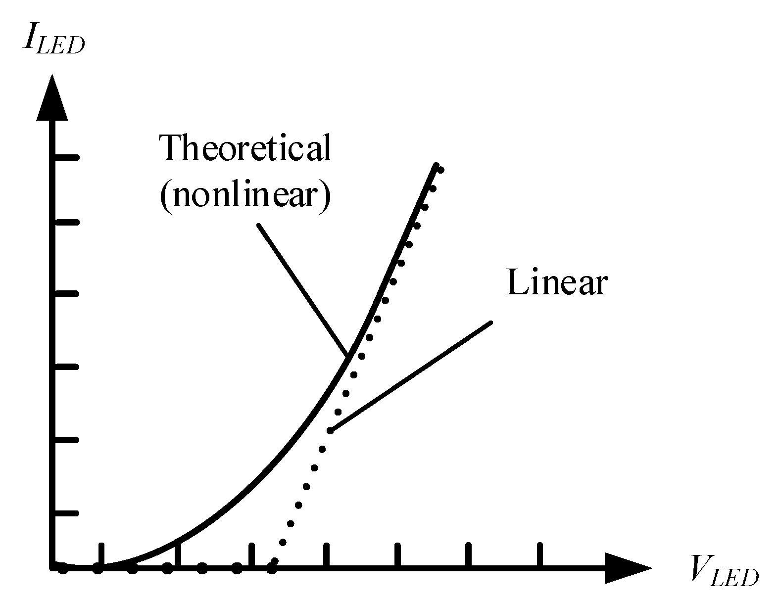
The rapid progress in the LED development have been attributed to significant improvement in the device efficiency lately [7,8]. The improvement of internal quantum efficiency has played a key role in the LED development. Specifically, the internal quantum efficiency of the InGaN LEDs have been improved by using large overlap quantum well concept or new active material concept [9]. One of the most significant features of LEDs is the possibility to adjust to a specific wavelength to exactly control for the light quality. The resulting monochromatic spectrum may be needed in photomorphogenic responses (growth, synthesis of phytochemicals) in plants. Spectral compositions of high-pressure sodium and compact fluorescent light lamps are broad and uncontrolled while LED system may produce monochromatic light, long wavelength emission, transition wavelength, or tailored broad spectrum. The lack of delay in start-up of LEDs allows the use of high frequency pulsing and dimming important for photoperiodic responses, for example [10]. The LEDs are thus superior in environment protection, commercial applications and energy saving aspects. LEDs are driven by direct current (DC) voltage. An alternating current (AC)–DC power factor correction (PFC) converter must be applied for regular grid power to be used for LED light sources. However, for the driver, LEDs perform a nonlinear load, and the current–voltage (I–V) curve can be presented as exponential function in Equation (1):
where ILED is the forward current, VLED is the forward voltage, Isat: is the saturation current or critical current of the diode, q: number of the electric charges of the electron (=1.62 × 10⁻¹⁹), k: the Boltzmann constant (=1.38 × 10⁻²³) and T is the absolute temperature in degrees Kelvin (=273 + room temperature). Compared with a regular linear load, a nonlinear load is more difficult for users to design; the curvature increases the possibility of errors between simulation and practice (Figure 1) [11].
Applying the linear model to conduct simulation and design will result in notable differences from the actual LED curve. Therefore, the objective of this study was to determine a simulation method that enables the researcher to obtain data similar to actual ones without going through complex measuring processes as well as minimize the discrepancy between simulation and actual data.
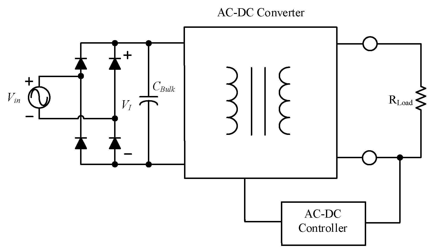
Although the energy-saving performance of LED light sources is superior to that of conventional light sources, specific voltage-converting equipment is required in order to achieve the rated voltage and current required for LEDs to function properly. In addition, different LED luminaires are equipped with different converters. The use of an adequate and highly efficient LED power converter is critical. Figure 2 presents the framework of the flyback converter used in this study. The PFC circuit is added to the first stage because most modern electrical appliances have nonlinear loads, which result in phase angle deviation between the input voltage and input current and causes a reduction in the power factor. In addition, the input current generates an enormous amount of harmonic waves after a bridge rectification. The power supply quality and system efficiency tend to be low under the influence of low power factor and large amounts of harmonic waves. Therefore, existing power supplies and drivers on the market are equipped with PFC circuits to suppress harmonic waves of the current and increase the power factor to prolong the life expectancy [12].
The present study investigated the optimal combination design of the LED matrix applicable to the flyback driver. This study also serves as a step-by-step guide for readers, from theory-induction to circuit design and Taylor series simulation analysis of loads, for effectively and quickly understanding this research and reducing the time required for the design process.
2. Single-Stage PFC Circuit
2.1. Boundary Conduction Current Mode Control
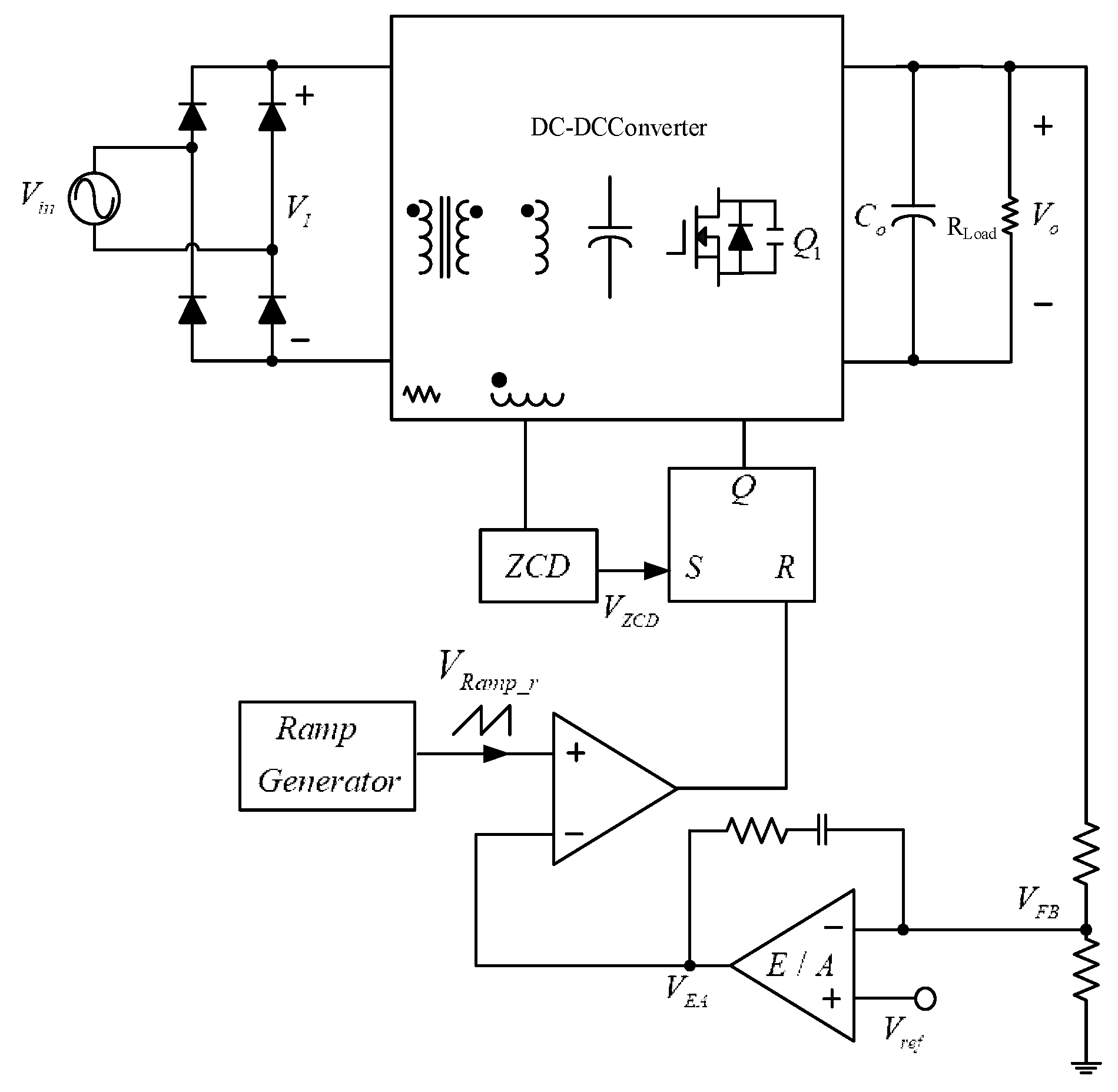
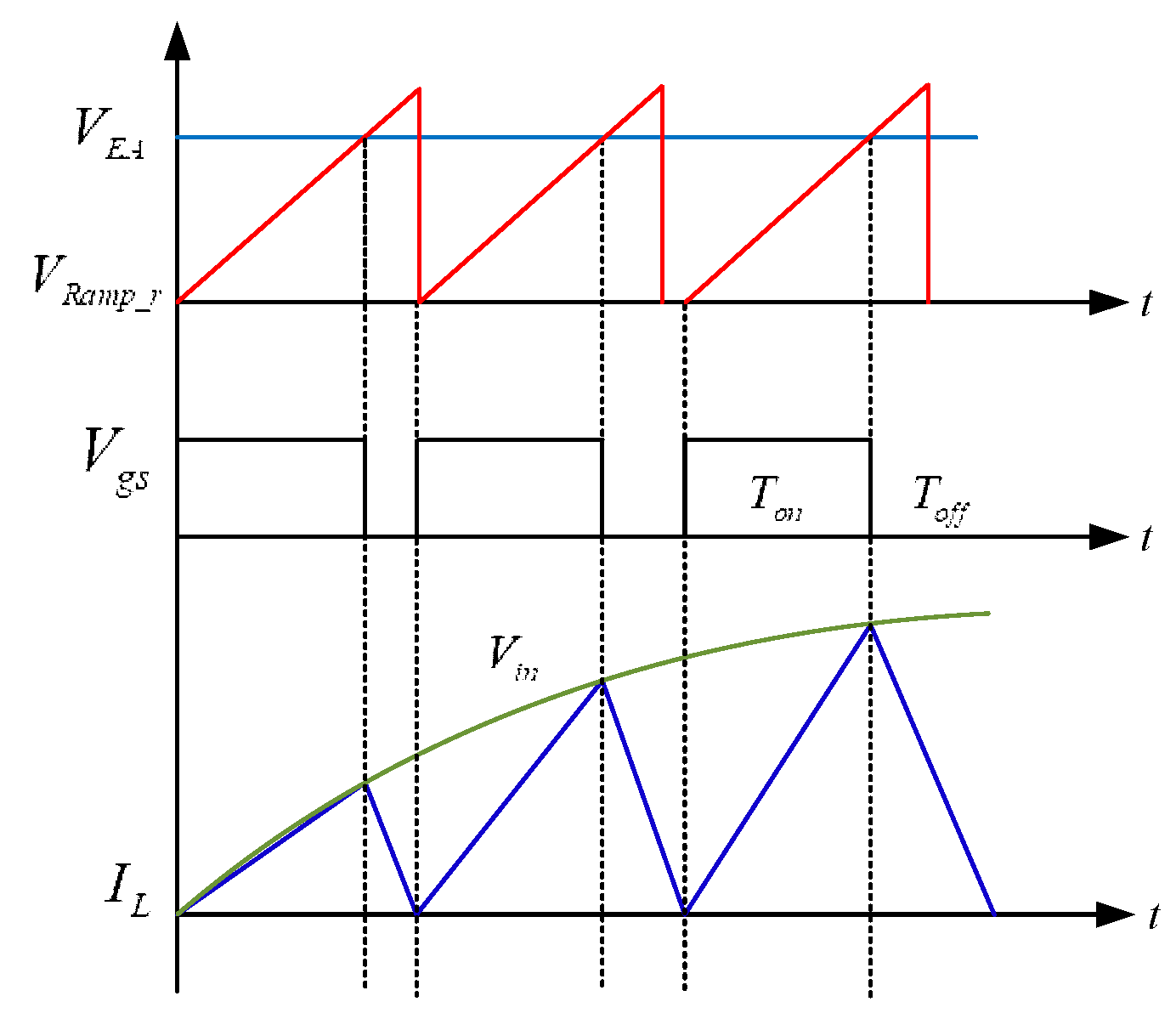
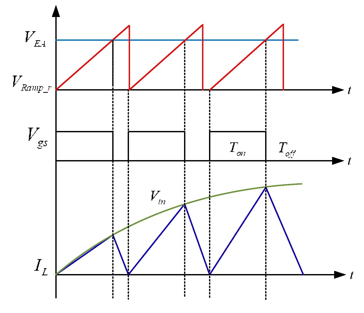
The circuit and relevant waveforms of voltage mode control (VMC) [13,14,15] are presented in Figure 3 and Figure 4. The bandwidth of the error amplifier (E/A) is also set remarkably lower than the frequency of input voltage, and VEA is a DC voltage with extremely low ripples. After comparing the reference voltage Vref with the feedback voltage VFB, which is obtained at the output end Vo by dividing the voltage by resistances, the E/A is employed to obtain the amplified DC signal VEA, which is drawn to compared with VRampr (Figure 3). When VRampr < VEA, the power switch is on and the inductor is storing energy; whereas when the voltage VRampr increases to ≥ VEA, the R end of the RS flip-flop is instantly triggered to turn the power switch off and the inductor begins to release energy. Till the energy stored in the inductor runs out, the zero current detector (ZCD) circuit sends a wake-up signal CZCD to the S end of the RS flip-flop. Next, the RS flip-flop Q outputs a high-level signal to turn the switch back on. This action is repeated to achieve output voltage stabilization and regulation as well as high power factor. This method employs variable-frequency control in which a constant on-time Ton (Figure 4) is retained and the switching frequency varies with the input voltage and output load. The cost of VMC is lower because the multiplier is needless. In addition, the current sensing resistance in VMC is reserved simply for over-current protection.
2.2. Main Device Parameter Design
The system framework established in this study is the 120 W flyback LED driving circuit (Figure 5). The specifications of this framework are listed in Table 1.
2.2.1. Selection of the MOSFET Power Switch Q1
The selection of the MOSFET concerns the setting of transformer turn ratio n, which is a trade-off condition; that is, a higher n corresponds to a higher power factor and lower total harmonic distortion (THDs). However, as shown in Equation (2), a higher n corresponds to greater stress of the drain–source voltage Vds max on the switch and consequently incurring greater cost:
where Vin max: the maximum effective value of the input voltage; ΔV: the voltage of the leakage inductance effect, which is usually set at half of the mapped voltage VR (from the output voltage).
By the way, the endurance of the maximum conducting current of the switch, Ids max = IpeakP, must also be taken into consideration.
2.2.2. Selection of the Secondary-Side Output Rectifier Diode DS
A higher n corresponds to a lower reverse voltage of the secondary-side diode Vdioder(max), as indicated in Equation (3):
The endurance of the maximum conducting current of the secondary side, IDmax = nIpeakP, must also be taken into consideration when choosing the rectifier diode.
2.2.3. Selection of the Bridge Rectifier B
The input voltage of a bridge rectifier is a low-frequency signal; therefore, devices with high-frequency features are not required. Generally, only the peak input voltage and peak input current must be considered.
2.2.4. Selection of the Input Capacitor CBULK
The most commonly selected input capacitor CBULK is 1 µF or lower, which performs as a high-frequency filter capacitor rather than a rectifier; therefore, the capacitance is regarded as highly resistant for the input power frequency. Consequently, the voltage signal of CBULK after bridge rectification forms an M-shaped wave.
2.2.5. Selection of the Output Capacitor Co
Because the output voltage ripple of the output capacitor Co is twice the input power frequency, the capacitance of the PFC circuit established in this study is greater than that of a regular flyback converter and is given by Equation (4):
where ΔVout: the ripple voltage, which is usually set with a peak-to-peak value of 1 V; fL: the input power frequency and IOmax: the maximum output current.
The output capacitor can be connected in parallel to reduce the equivalent series resistance and the output ripples. According to the calculation, the specifications and parameters of the main devices are provided in Table 2.
3. Simulation of a Taylor Series
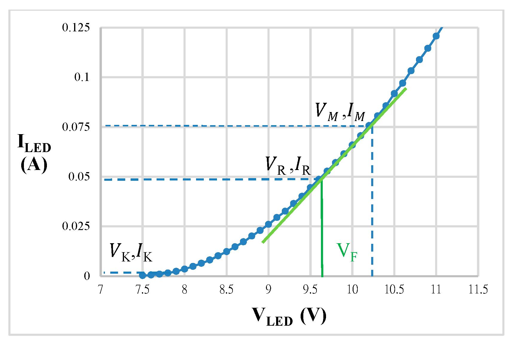
Figure 6 presents the single-stage LED model and Figure 7 presents the I–V curve of the maximum and minimum operating point of the LED, which help to derive the Taylor series [16,17,18].
Equation (5) presents the nonlinear LED current–voltage characteristic. For VF >> VT, Equation (5) can be simplified as Equation (6), where VT is the thermal voltage, which is approximately 25 mV at room temperature:
where IF: forward current, VF: forward voltage, Isat: saturation current or critical current of the diode, which equals the current when the voltage VF exceeds VT in the negative direction and is usually 10−12 A, n: ideality factor of the diode, which falls between 1 and 2 for a silicon diode, q: number of the electric charges of the electron (=1.62 × 10⁻¹⁹), k: Boltzmann constant (=1.38 × 10⁻²³), T: absolute temperature (in K = 273 + room temperature) and VT: thermal voltage of the LED [19]:
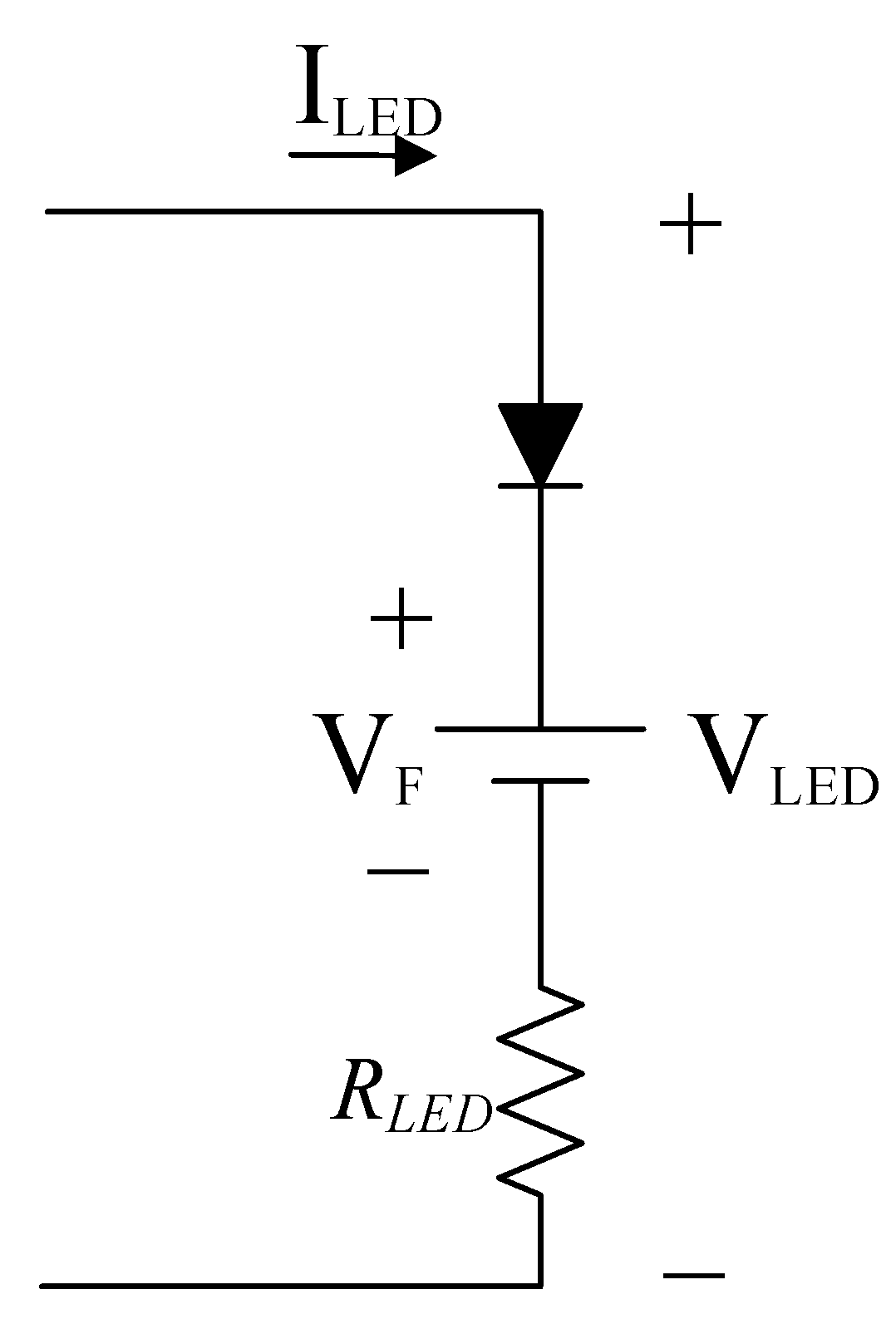
Equation (8) is obtained by using the LED model presented in Figure 6 and represents the relationship between the voltage across the LED and forward voltage of the LED, where RLED is the internal resistance of the LED. Equation (9) can be obtained by substituting Equations (6) and (7) into Equation (8):
The maximum operating point (VM,IM), minimum operating point (Vk,IK), and rated operating point (VR,IR) can be obtained from the datasheet of the luminaire. Figure 7 presents the I–V curve marked with the aforementioned operating points. The rated and maximum operating points are subsequently connected to form a straight line; the internal resistance (RLED) parameter is obtained by calculating the slope of said line with Equation (10):
The ideality factor (n) is obtained by substituting Equation (10) into Equation (9) to yield Equation (11):
The saturation current (Isat) is obtained by substituting the minimum operating point (VM,IM) into Equation (6), as given by Equation (12):
To obtain an accurate I–V curve, the Taylor series is required to obtain the nonlinear load. The used equation is given by Equation (13), where the unknown parameters are obtained from Equations (10)–(12) and the forward current obtained from simulation is also substituted into the equation. Additionally, j denotes the number of levels. The simulated current varies with the number of levels set by the Taylor series.
4. System Simulation
4.1. Introduction of the Simulation
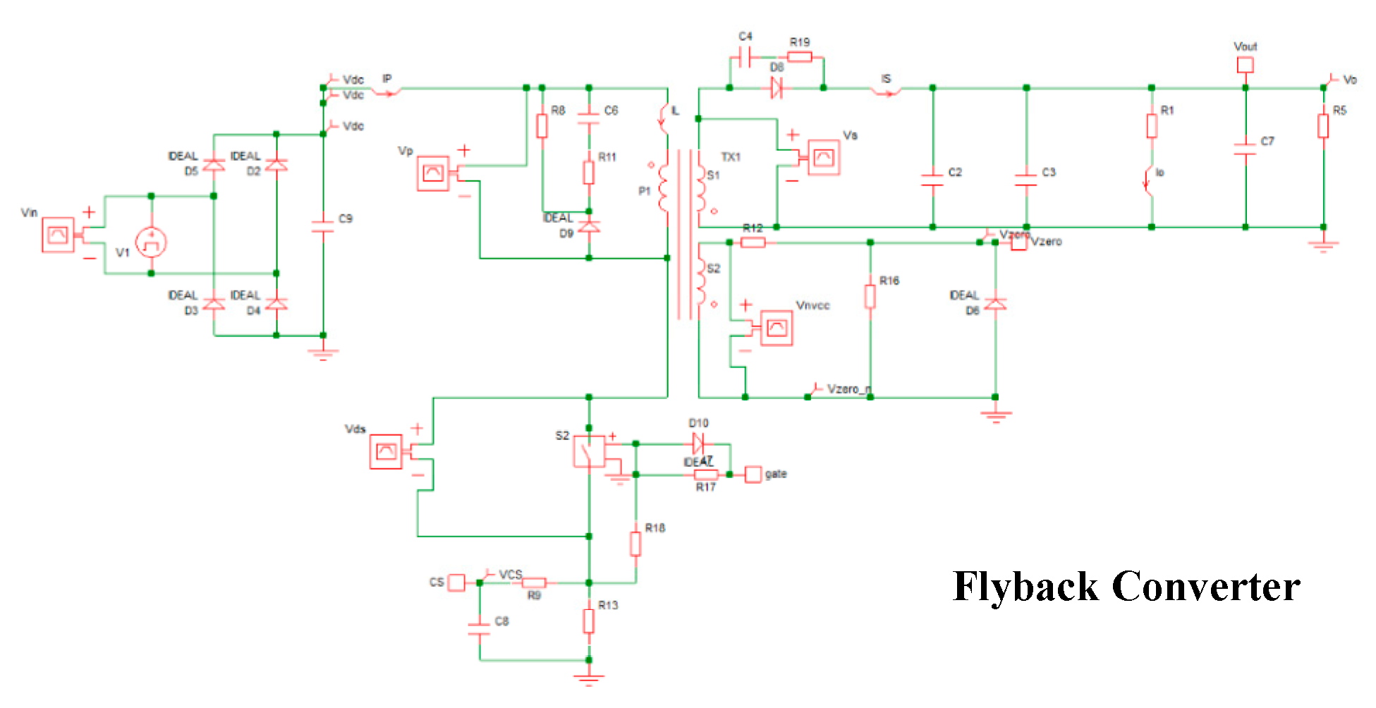
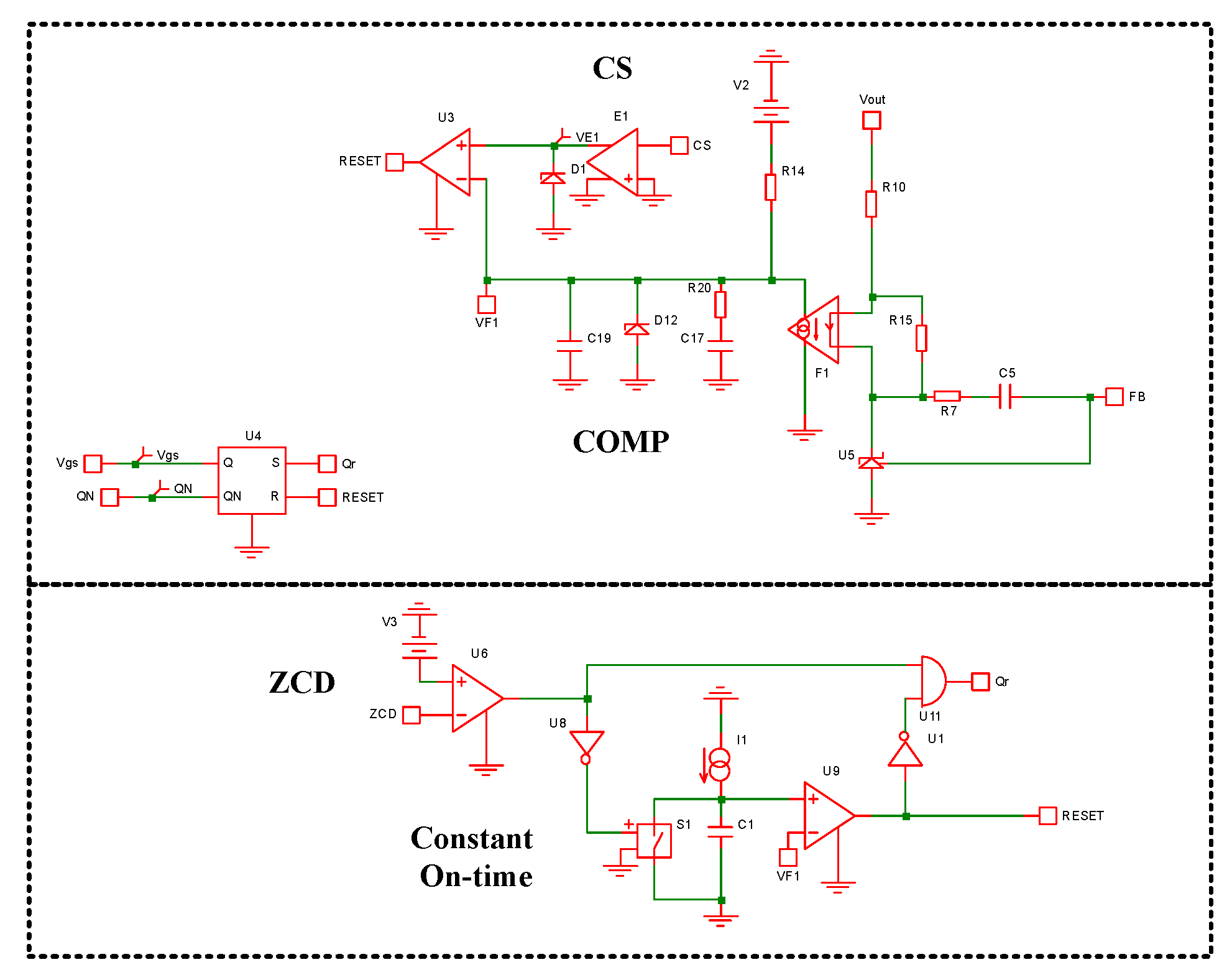
The simulation software employed in this study is SIMetrix/SIMPLIS. Figure 8 presents the flyback PFC circuit simulation framework, which contains the same main circuit as a regular flyback converter. In addition, the circuit established in this study contains a ZCD, which enables soft-switching of the switch, reduces loss, and improves overall efficiency of the system. The characteristic of this circuit is similar to that of the quasi-resonant flyback converter. Both switches are triggered when the voltage Vds reaches the wave trough.
Figure 9 presents the SIMPLIS circuit control block module of PFC function and closed-loop feedback. The main control functions include four control blocks: 1. switch current sensor signal (CS), 2. closed-loop feedback signal (COMP), 3. ZCD function for the auxiliary winding of the transformer, and 4. COT control of PFC [20,21].
4.2. Simulation Results
The LED model as the output load is referenced by Figure 6 in Section 3 Using this model in the SIMPLIS simulation is to emulate the realistic LED I–V curve. The simulation conditions include full-range input voltage to demonstrate the system stability is well-performed and check the voltage and current of LED approximate to the Mathcad computation.
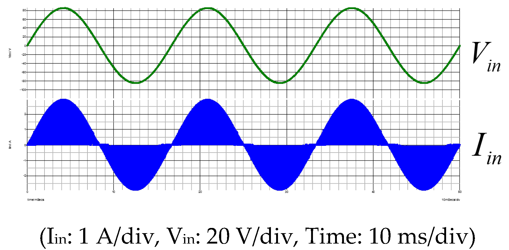
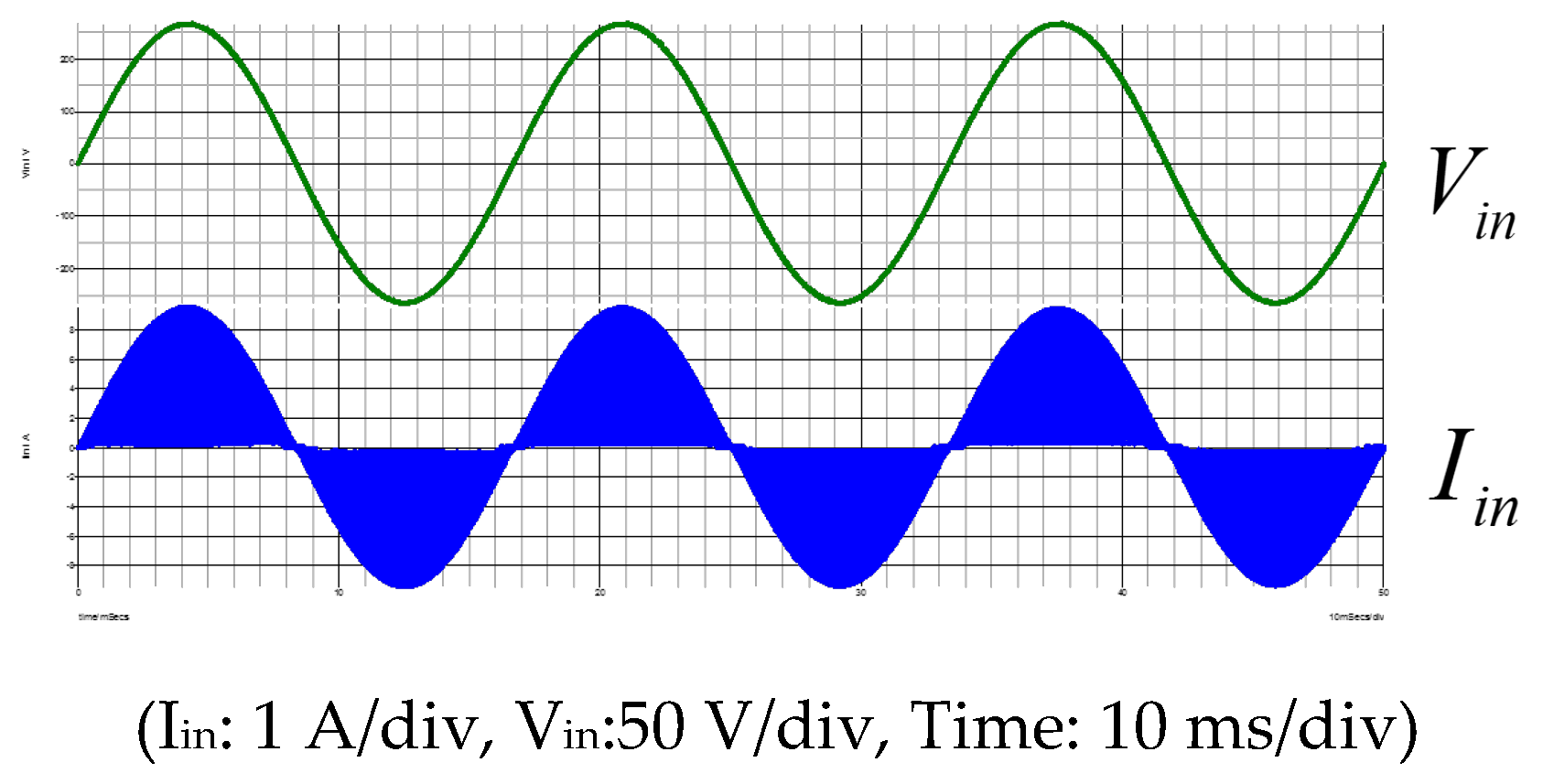
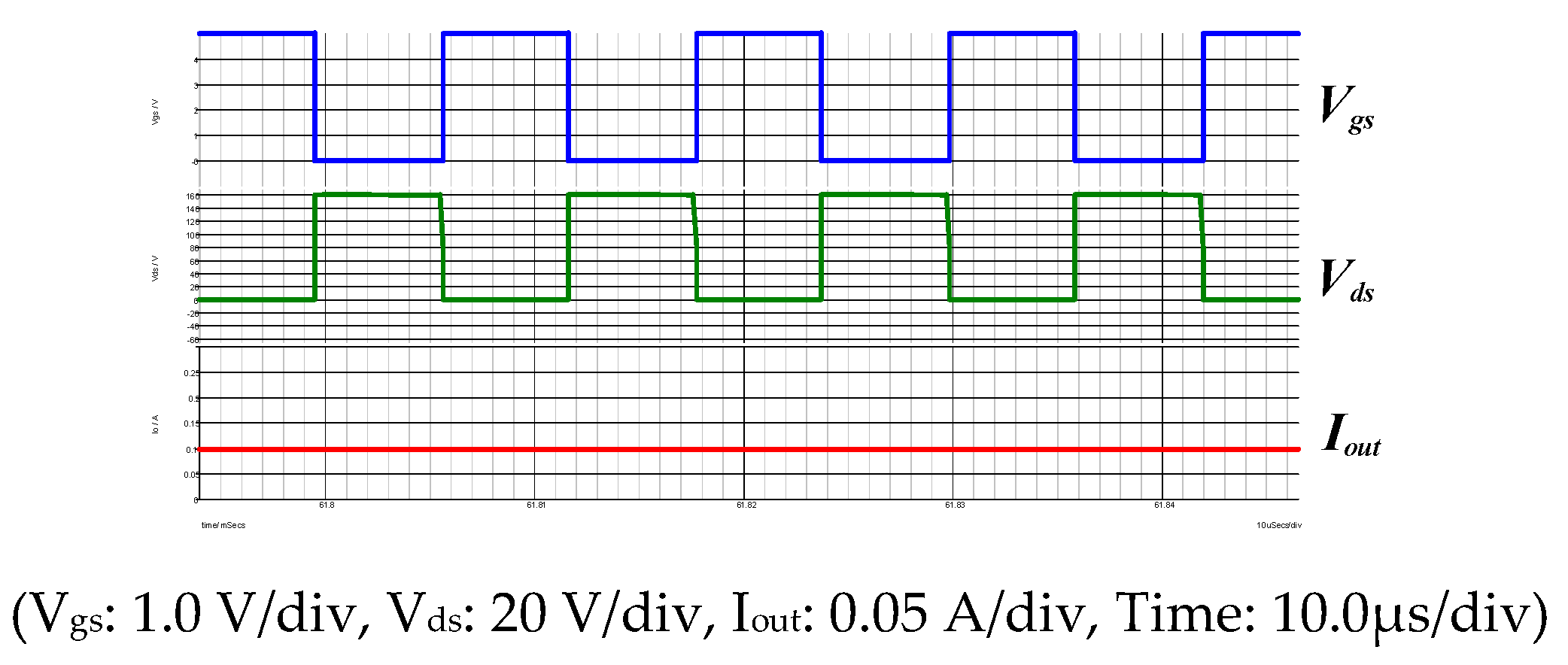
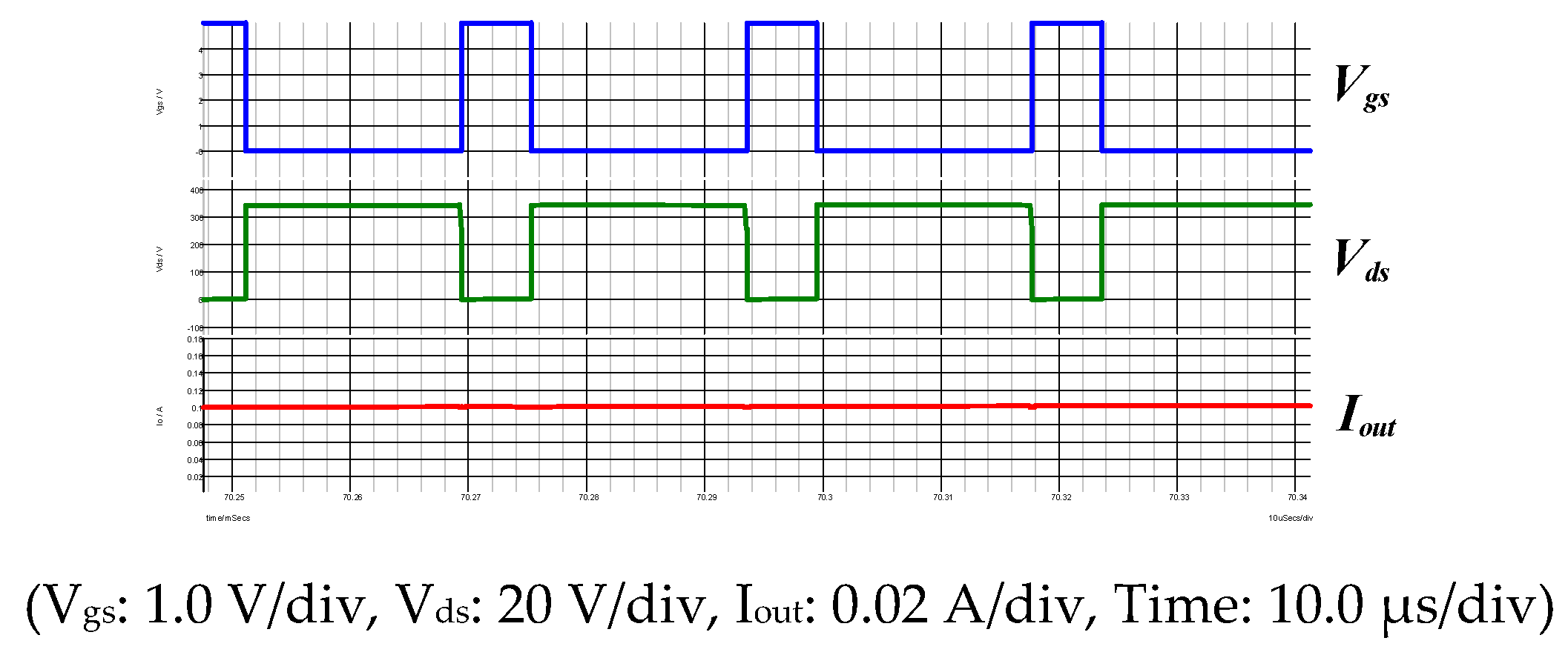
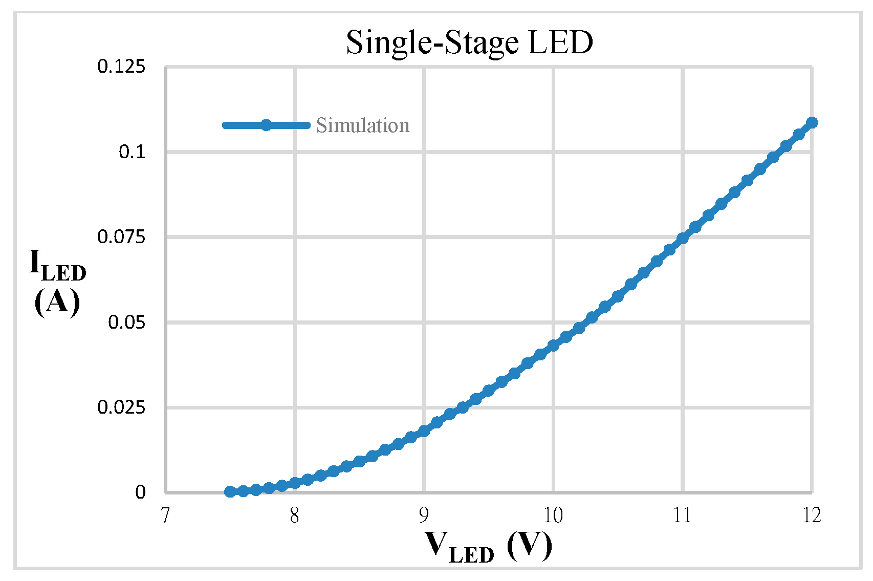
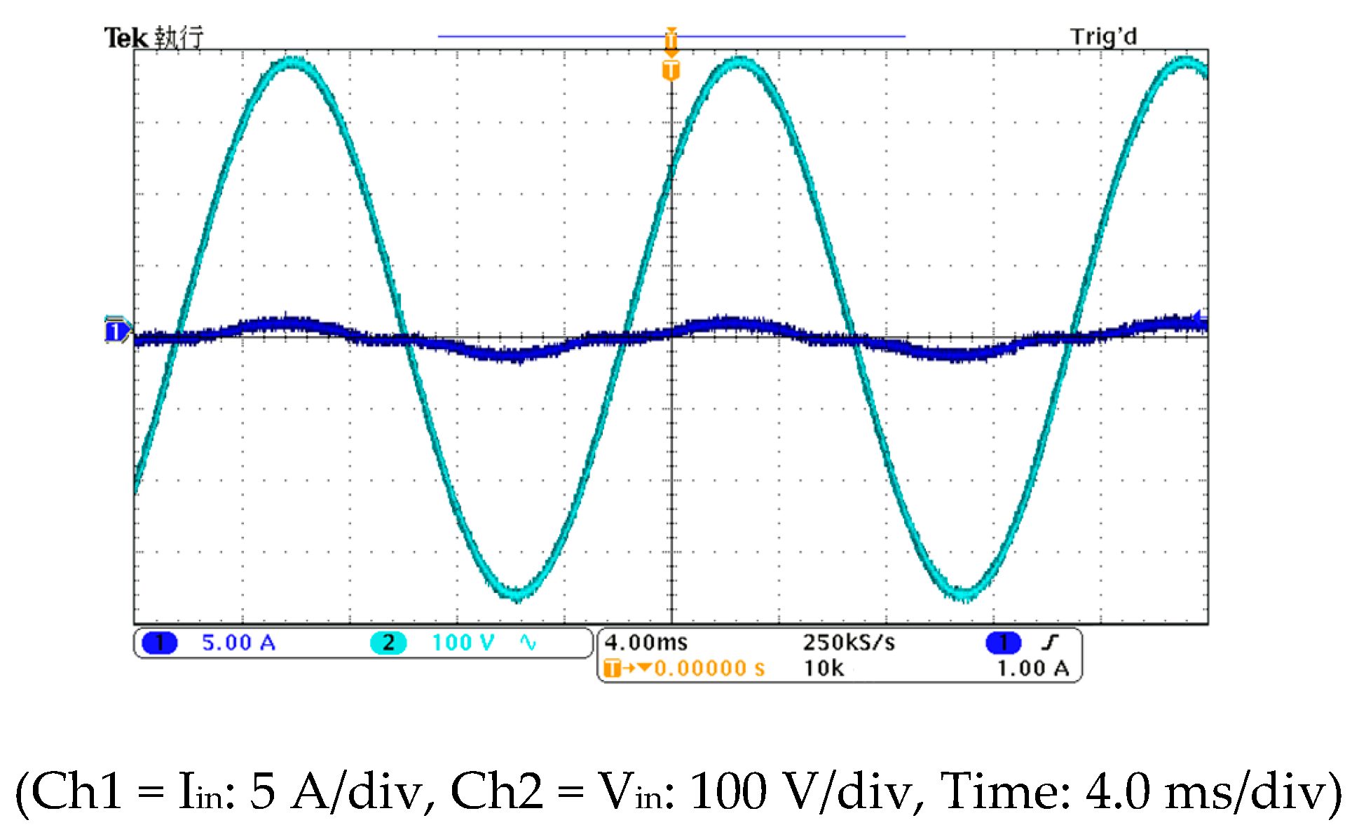
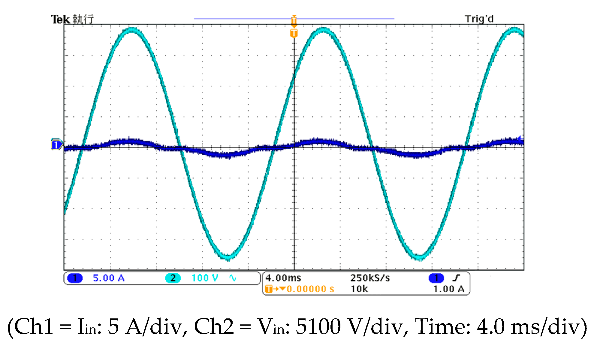
First, Figure 10 and Figure 11 show the whole system works under the normal operation conditions. The maximum output load of this system is 120 W and the input voltage is set by 85 V and 265 V individually. The input voltage and current are completely in phase and the output voltage across LED is kept at the rated voltage of 12 V. Figure 12 and Figure 13 show the current flowing through LED maintains at 0.1085 A whether the input voltage is 85 V or 265 V. The simulation results prove the system is validated for a single-stage flyback PFC converter. Next, in order to plot the simulated single-stage LEB I–V curve as shown in Figure 14, the voltage on LED is designated as the independent variable and the current through LED naturally becomes the dependent variable. After repeating several times of simulation, the acquisition of data of LED voltage and current can plot the I–V curve, which can be a benchmark for experimental results afterwards.
5. Waveform Measurements and Actual Data
5.1. Test Results of the Circuit
5.2. Comparison of the Taylor Series Simulation and Actual Results
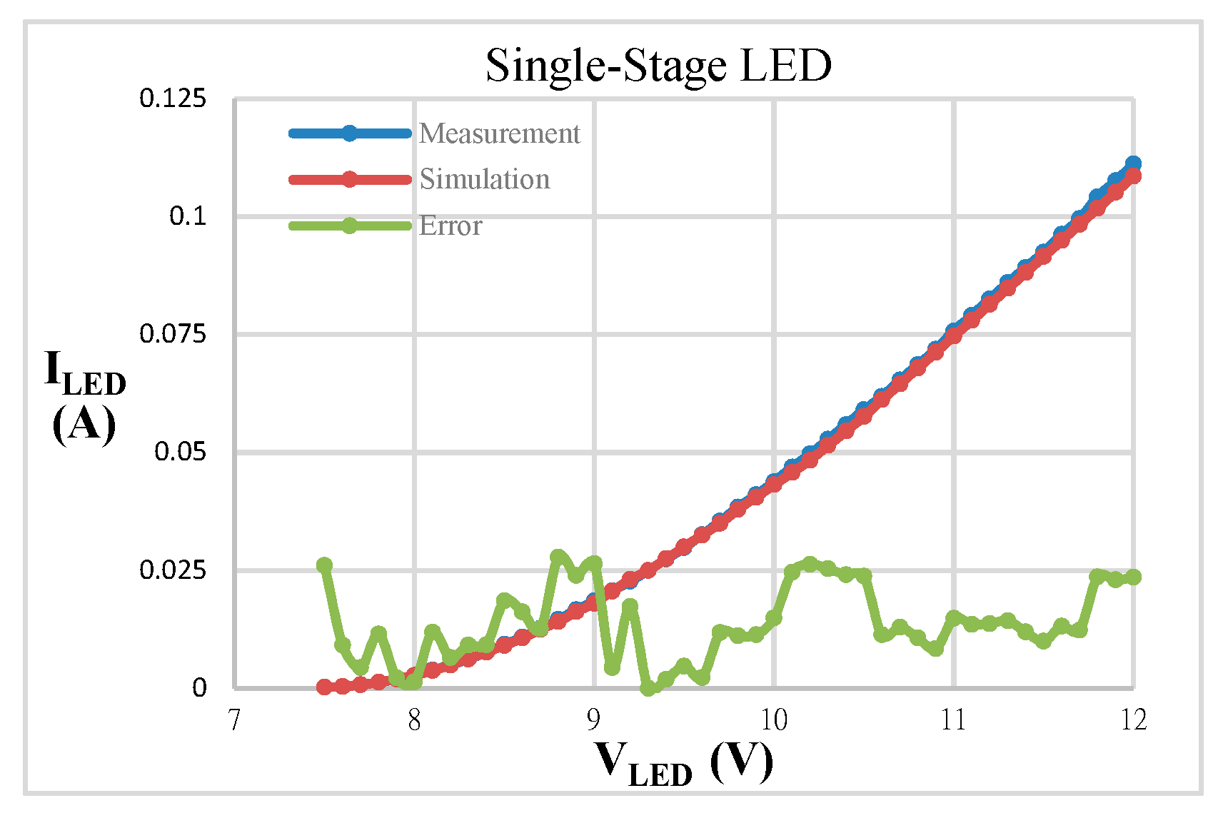
The data from the simulation with the Taylor series analysis and actual testing were illustrated as below. Figure 19 and Figure 20 present comparisons of the single-stage and multi-stage results, respectively. This method reduced the error to less than 3%.
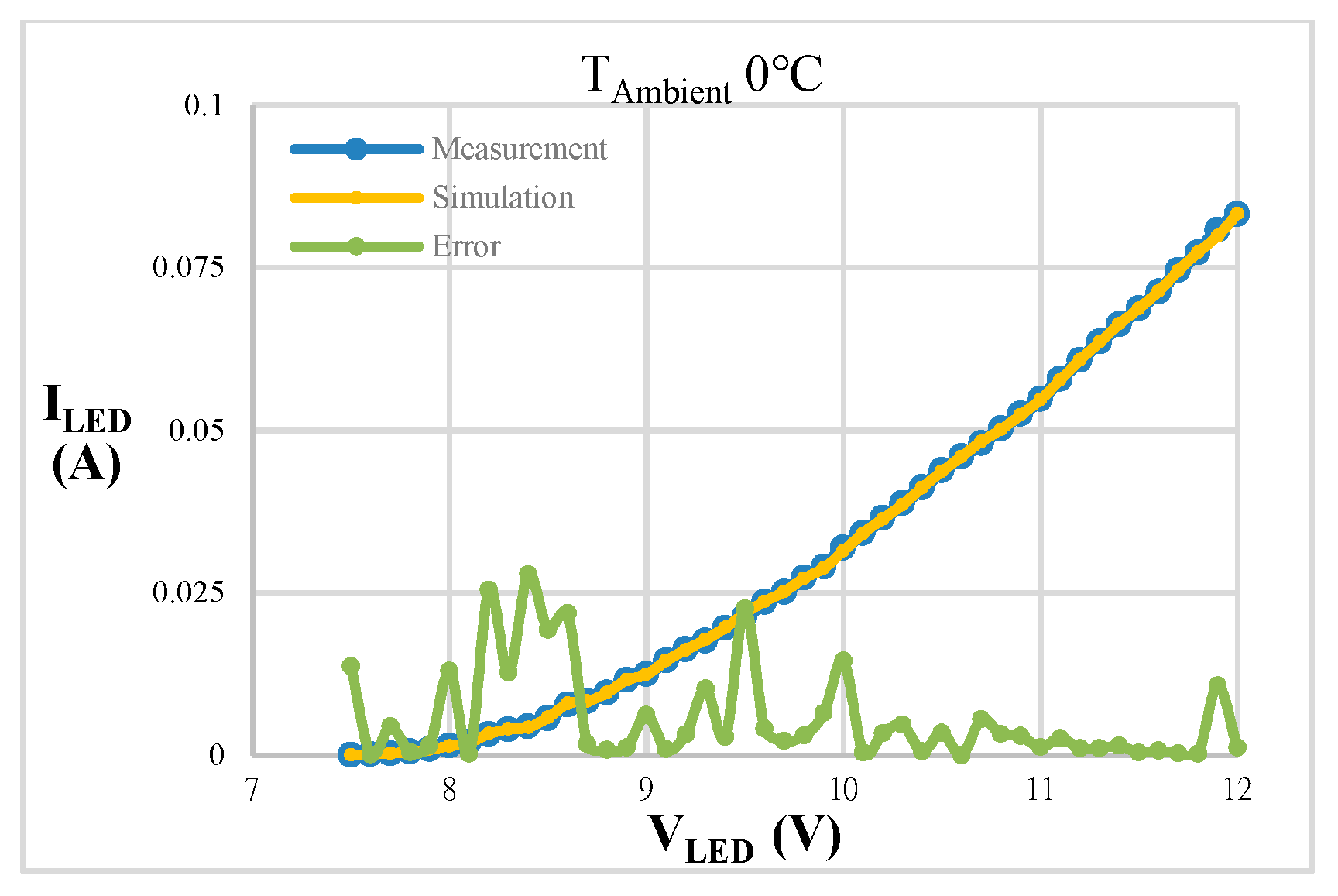
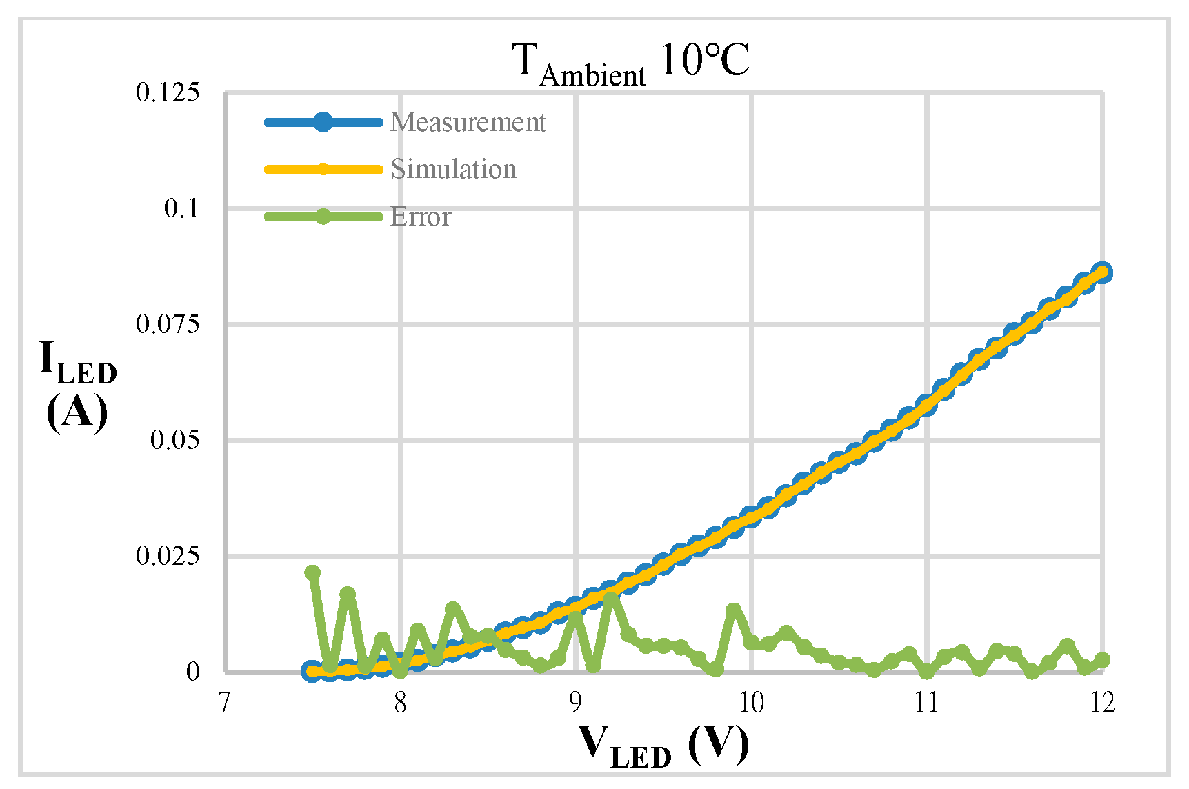
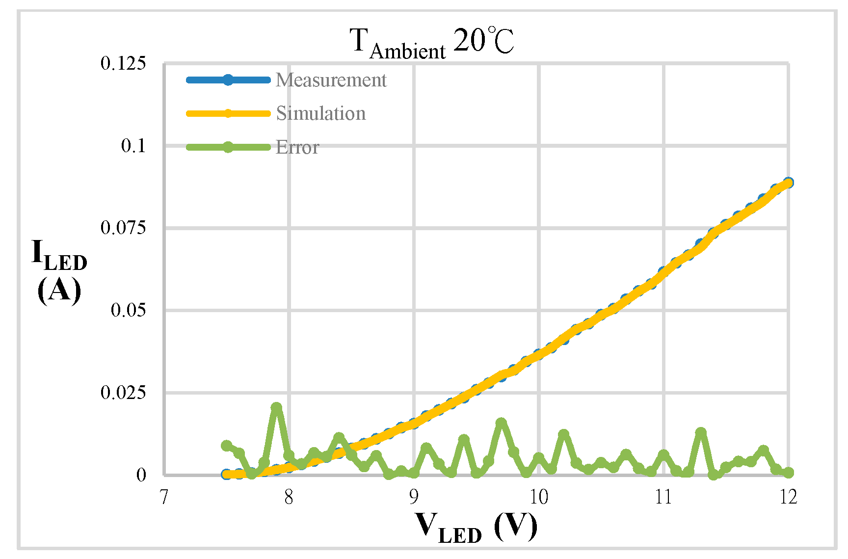
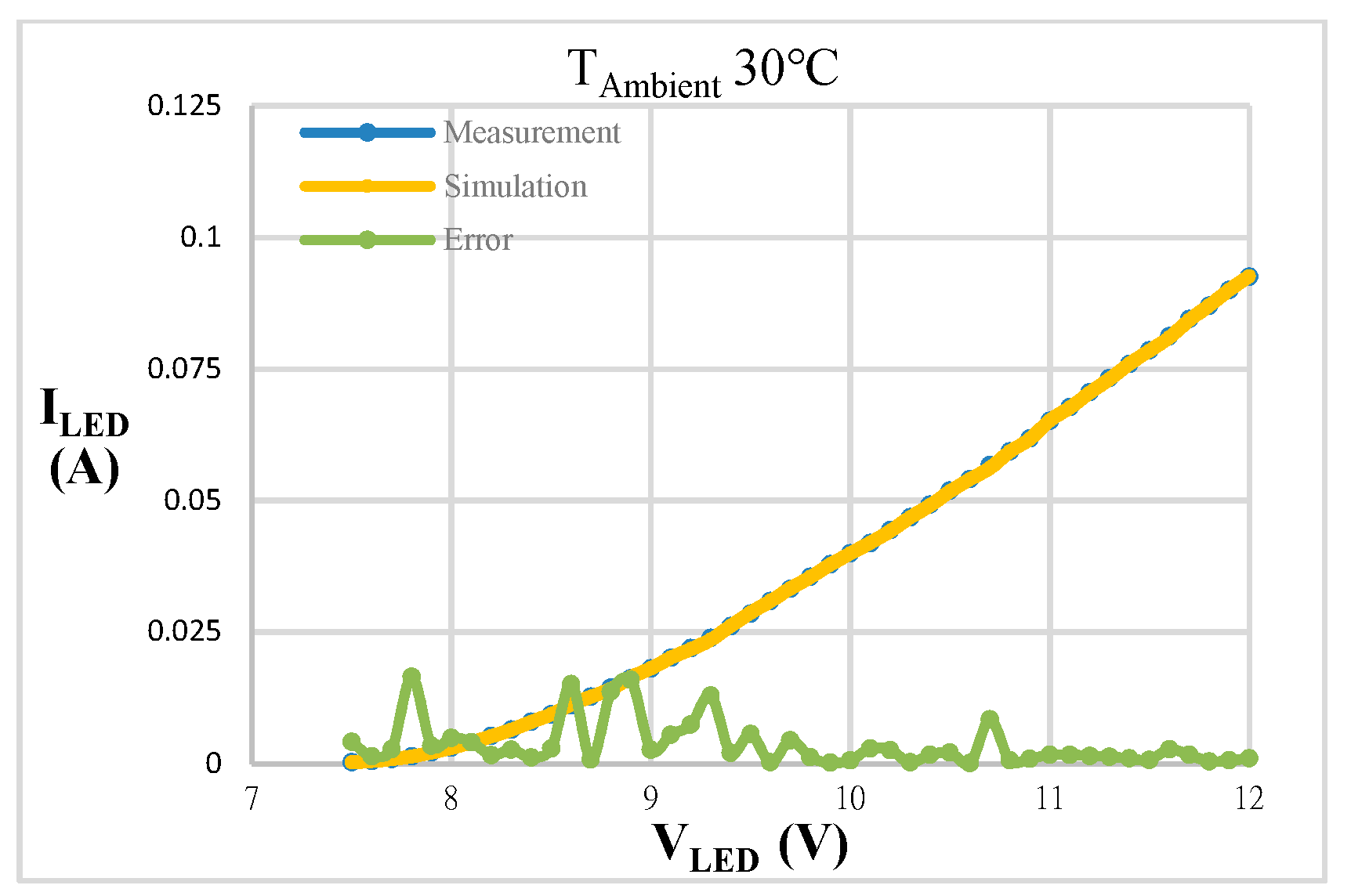
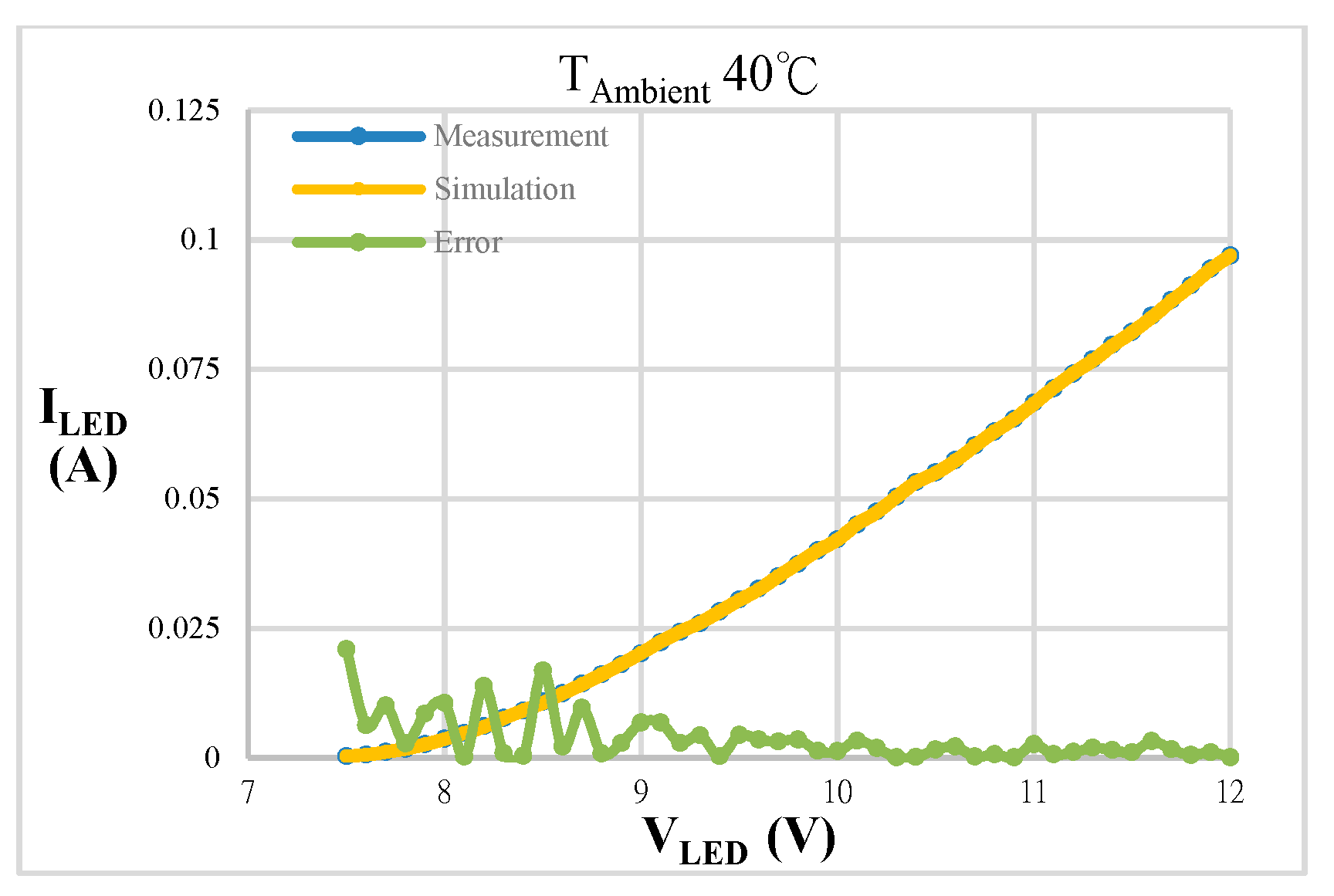
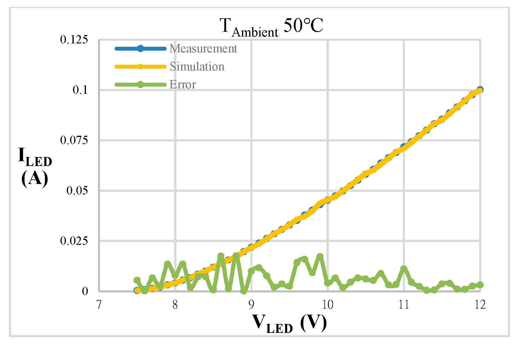
Because the LED forward voltage (VF) is a temperature dependent factor, the next work is to check if the variation of ambient temperature (TAmbient = 0 °C–50 °C) affects the errors between the simulated and measured results. When TA descends from 30 to 0 Celsius degrees, which means VF gets larger by the lower degrees as shown in Figure 21, Figure 22 and Figure 23, the errors are still below 2.14%. On the contrary, when TA ascends from 30 to 50 °C, the errors are below 2.09% in spite of the smaller VF, as shown in Figure 24, Figure 25 and Figure 26. The test results demonstrate the errors between Taylor series simulation and actual testing results can achieve temperature independent.
6. Conclusions
The Taylor series load simulation analysis established in this study together with the flyback LED driver could quickly obtain results for the actual circuit through simulations. Furthermore, the inclusion of thermal parameter adjustment could further increase the similarity between the system simulation and actual design to reduce error. Through the analysis in this study, products designed for use at different temperatures can establish the precise simulation module to predict their actual performance in order to simplify the circuit design process and meet demands for system safety, reliability, and adjustability. In addition, the power converter designed in this study can be used under a wide input voltage range (85–265 V), and the luminaire output is fit for 120 W LEDs for commercial lighting products. The present study first details an explicit analysis of the working principles of the LED driver and then uses mathematical models to derive equations and calculate the parameters of each device. The simulation software SIMPLIS was used to establish emulated power converter modules. The simulation results can precisely demonstrate the real waveform of each node in advance to improve the yield rate of the system design and reduce the time required for circuit debugging. Finally, the actual parameters are substituted into the prototype circuit to complete the circuit testing.
Author Contributions
M.-T.K. and M.-C.T. played important roles during the optimal combination design and partially wrote the paper. M.-C.T. ran the simulation and did the experiment and M.-T.K. reviewed the manuscript. All authors have read and agreed to the published version of the manuscript.
Funding
This work was supported by the National Science Council of Taiwan under Contract MOST 108-2221-E-011-082-MY3.
Acknowledgments
The authors would like to thank Leadtrend Technology Corp. for the support on chip fabrication, measurement, and verifications.
Conflicts of Interest
The authors declare no conflict of interest.
References
- Hall, R.N.; Fenner, G.E.; Kingsley, J.D.; Soltys, T.J.; Carlson, R.O. Coherent light emission from GaAs junctions. Phys. Rev. Lett. 1962, 9, 366–368. [Google Scholar] [CrossRef]
- Lenk, R.; Lenk, C. Practical Lighting Design with LEDs; Wiley: Hoboken, NJ, USA, 2011. [Google Scholar]
- Feola, L.; Langella, R.; Testa, A. A new frequency approach for light flicker evaluation in electric power systems. EURASIP J. Adv. Signal Process. 2015, 85. [Google Scholar] [CrossRef] [Green Version]
- Ahn, Y.D.; Bae, S.; Kang, S.-J. Power Controllable LED System with Increased Energy Efficiency Using Multi-Sensors for Plant Cultivation. Energies 2017, 10, 1607. [Google Scholar] [CrossRef]
- Zhou, Y.; Qian, S.; Zhu, Q.; Huang, L.; Hu, A.P. A Simple Brightness and Color Control Method for LED Lighting Based on Wireless Power Transfer. Access IEEE 2018, 6, 51477–51483. [Google Scholar]
- Cardes, J.; Garc, D.; Corominas, E.L.; Calleja, A.J. Low Cost Intelligent LED Driver for Public Lighting Smart Grids. In Proceedings of the 2013 International Conference on New Concepts in Smart Cities: Fostering Public and Private Alliances (SmartMILE), Gijon, Spain, 11–13 December 2013; pp. 1–6. [Google Scholar]
- Crawford, M.H. LEDs for Solid-State Lighting: Performance Challenges and Recent Advances. IEEE J. Sel. Top. Quantum Electron. 2009, 15, 1028–1040. [Google Scholar] [CrossRef]
- Denbaars, S.P.; Feezell, D.; Kelchner, K.; Pimputkar, S.; Pan, C.C.; Yen, C.C.; Tanaka, S.; Zhao, Y.; Pfaff, N.; Farrell, R.; et al. Development of gallium-nitride-based light-emitting diodes (LEDs) and laser diodes for energy-efficient lighting and displays. Acta Mater. 2013, 61, 945–951. [Google Scholar] [CrossRef]
- Tan, C.K.; Borovac, D.; Sun, W.; Tansu, N. InGaN/Dilute-As GaNAs Interface Quantum Well for Red Emitters. Sci. Rep. 2016, 6, 19271. [Google Scholar] [CrossRef] [PubMed] [Green Version]
- Winder, S. Power Supplies for LED Driving; Butterworth-Heinemann: Oxford, UK, 2008. [Google Scholar]
- Lin, R.-L.; Tsai, J.-Y.; Alonso, J.M.; Gacio, D. Four-Parameter Taylor Series-Based Light-Emitting-Diode Model. IEEE J. Emerg. Sel. Top. Power Electron. 2015, 3, 581–588. [Google Scholar]
- Bor-Ren, L.; Ta-Chang, W.; Huann-Keng, C. Novel AC Line Conditioner for Power Factor Correction. IEEE Trans. Aerosp. Electron. Syst. 2004, 40, 168–179. [Google Scholar] [CrossRef]
- Nalla, S.L.; Hess, H.L.; Buck, K.M.; Mentze, E.J. Flyback converter with voltage control mode on chip for portable applications. In Proceedings of the IEEE Microelectron. Electron Devices, Boise, ID, USA, 15 April 2005; pp. 80–83. [Google Scholar] [CrossRef]
- Juang, K.C.; Chiang, S.J.; Xiao, W.M. A grid-tied flyback-based PV inverter with BCM variable frequency voltage mode control. In Proceedings of the 2012 International Symposium on Intelligent Signal Processing and Communications Systems, Taipei, Taiwan, 4–7 November 2012. [Google Scholar]
- Lai, J.S.; Chen, D. Design Consideration for Power Factor Correction Boost Converter Operating at the Boundary of Continuous Conduction Mode and Discontinuous Conduction Mode. In Proceeding of IEEE Applied Power Electronics Conference, San Diego, CA, USA, 7–11 March 1993; pp. 267–273. [Google Scholar]
- Lin, R.-L.; Liu, S.-Y.; Chiang, H.-W. Optimal LED array combination for single-loop CCM boost driver. In Proceedings of the 2012 IEEE Industry Applications Society Annual Meeting, Las Vegas, NV, USA, 7–11 October 2012. [Google Scholar]
- Lin, R.-L.; Liu, S.-Y.; Lee, C.-C.; Chang, Y.-C. Taylor-Series-Expression-Based equivalent circuit models of LED for analysis of LED driver system. IEEE Trans. Ind. Appl. 2013, 49, 1854–1862. [Google Scholar] [CrossRef]
- Lin, R.-L.; Chen, Y.-F. Equivalent circuit model of light-emitting diode for system analyses of lighting drivers. In Proceedings of the 2009 IEEE Industry Applications Society Annual Meeting, Houston, TX, USA, 4–8 October 2009. [Google Scholar]
- Schubert, E.F. Light-Emitting Diodes; Cambridge Univ. Press: Cambridge, UK, 2003. [Google Scholar]
- Tzuen-Lih, C.; Li-Hsiang, L.; Ching-Nan, H.; Yu-Lun, C.; Jao-Hwa, K. High Power Factor Flyback Converter for LED Driver with Boundary Conduction Mode Control. In Proceedings of the 2010 5th IEEE Conference on Industrial Electronics and Applications, Taichung, Taiwan, 15–17 June 2010. [Google Scholar]
- Liu, Y.; Yin, S.; Pan, X.; Wang, H.; Wang, G.; Peng, J. Effects of Nonlinearity in Input Filter on the Dynamic Behavior of an Interleaved Boost PFC Converter. Energies 2017, 10, 1530. [Google Scholar]
Figure 1.
Low-frequency ripples.

Figure 2.
Converter framework.

Figure 3.
Block diagram of the VMC circuit.

Figure 4.
Voltage signal of the VMC.

Figure 5.
Voltage signal of the VMC.

Figure 6.
LED linear model.

Figure 7.
I–V curve of the maximum and minimum operating point of the LED.

Figure 8.
Flyback PFC circuit simulation framework.

Figure 9.
PFC and closed-loop control circuits.

Figure 10.
Simulation of Vin and Iin (Vin = 85 V).

Figure 11.
Simulation of Vin and Iin (Vin = 265 V).

Figure 12.
Simulation of Vgs, Vds and Iout (Vin = 85 V; Vout = 12 V).

Figure 13.
Simulation of Vgs, Vds and Iout (Vin = 265 V; Vout = 12 V).

Figure 14.
Simulated results of single-stage LEDs.

Figure 15.
Waveforms of and ().

Figure 16.
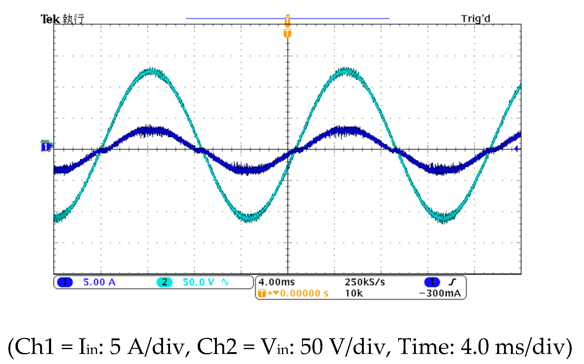
Waveforms of Vin and Iin (Vin = 110 V).

Figure 17.
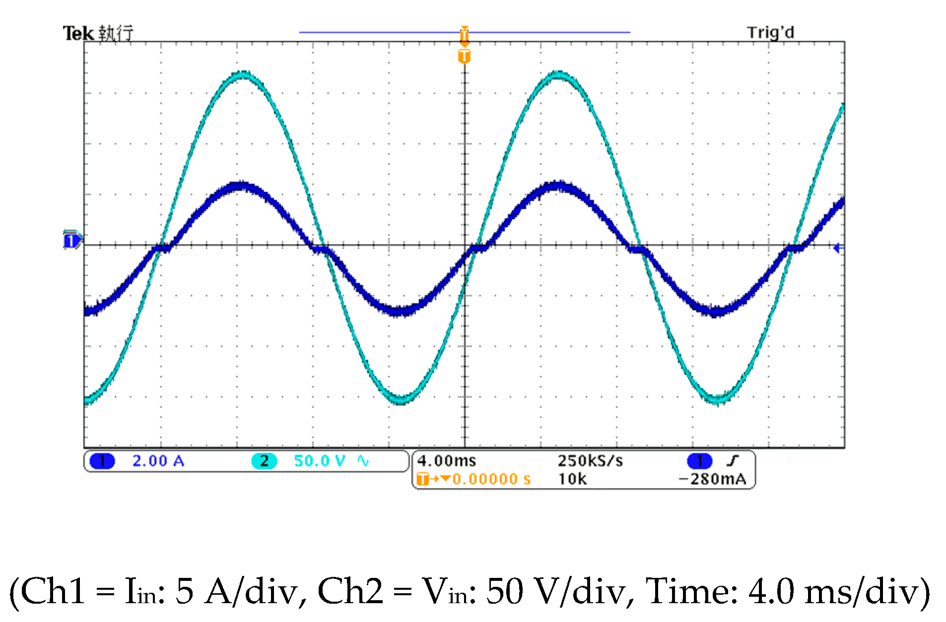
Waveforms of Vin and Iin (Vin = 220 V).

Figure 18.
Waveforms of Vin and Iin (Vin = 265 V).

Figure 19.
Measured and simulated results of single-stage LEDs.

Figure 20.
Measured and simulated results of multi-stage LEDs (24units).

Figure 21.
Measured and simulated results at TAmbient 0 °C.

Figure 22.
Measured and simulated results at TAmbient 10 °C.

Figure 23.
Measured and simulated results at TAmbient 20 °C.

Figure 24.
Measured and simulated results at TAmbient 30 °C.

Figure 25.
Measured and simulated results at TAmbient 40 °C.

Figure 26.
Measured and simulated results at TAmbient 50 °C.


Table 1.
System Parameters and Specifications.
| Hardware Parameter Setting | Specifications |
|---|---|
| Input voltage Vin (ac) | 85 V~265 V |
| Maximum output voltage Vo | 12 V |
| Maximum output current Io | 10 A |
| Minimum full-load switching frequency fs min | 50 kHz |
Table 2.
Parameters and specifications of the main devices selected for the circuit.
| Element | Specification | Model |
|---|---|---|
| Bridge rectifier B | 600 V/8 A | GBU806 |
| Input capacitor CBULK | 120 µF/400 V | Electrolytic capacitor |
| Output capacitor CO | 2040 µF/25 V | Electrolytic capacitor |
| Power switch MOSFET (Q1) | 600 V/13 A | 2SK3797 |
| Secondary side output diode DS | 200 V/0.25 A | BAS21 |
© 2020 by the authors. Licensee MDPI, Basel, Switzerland. This article is an open access article distributed under the terms and conditions of the Creative Commons Attribution (CC BY) license (http://creativecommons.org/licenses/by/4.0/).
Share and Cite
MDPI and ACS Style
Tsou, M.-C.; Kuo, M.-T. Optimal Combination Design of a Light Emitting Diode Matrix Applicable to a Single-Stage Flyback Driver. Energies 2020, 13, 5209. https://doi.org/10.3390/en13195209
AMA Style
Tsou M-C, Kuo M-T. Optimal Combination Design of a Light Emitting Diode Matrix Applicable to a Single-Stage Flyback Driver. Energies. 2020; 13(19):5209. https://doi.org/10.3390/en13195209
Chicago/Turabian StyleTsou, Ming-Chang, and Ming-Tse Kuo. 2020. "Optimal Combination Design of a Light Emitting Diode Matrix Applicable to a Single-Stage Flyback Driver" Energies 13, no. 19: 5209. https://doi.org/10.3390/en13195209
Note that from the first issue of 2016, this journal uses article numbers instead of page numbers. See further details here.