A Novel Step-Up Converter with an Ultrahigh Voltage Conversion Ratio


1
State Key Laboratory of Electrical Insulation and Power Equipment, School of Electrical Engineering, Xi’an Jiaotong University, Xi’an 710049, China
2
School of Electrical, Electronic and Computer Engineering, The University of Western Australia, Crawley, WA 6009, Australia
3
Xi’an Institute of Space Radio Technology, Xi’an 710100, China
*
Author to whom correspondence should be addressed.
Energies 2018, 11(10), 2693; https://doi.org/10.3390/en11102693
Submission received: 11 September 2018
/
Revised: 4 October 2018
/
Accepted: 8 October 2018
/
Published: 10 October 2018
(This article belongs to the Special Issue Control and Nonlinear Dynamics on Energy Conversion Systems)
Abstract
:A new step-up converter with an ultrahigh voltage conversion ratio is proposed in this paper. Two power switches of such a converter, which conduct synchronically, and its output voltage, which has common ground and common polarity with its input voltage, lead to the simple control circuit. No abrupt changes in the capacitor voltage and the inductor current of the proposed step-up converter mean that it does not suffer from infinite capacitor current and inductor voltage. Two input inductors with different values can still allow the proposed step-up converter to work appropriately. An averaged model of the proposed step-up converter was built and one could see that it was still fourth-order even with its five storage elements. Some theoretical derivations, theoretical analysis, Saber simulations, and circuit experiments are provided to validate the effectiveness of the proposed step-up converter.
1. Introduction
As part of a DC switching power supply, the step-up converter is important for transforming low input voltage into the desired high output voltage to satisfy the requirements of practical applications, such as photovoltaic (PV) systems, fuel-cell systems, etc. Step-up converters can be classified into two types: non-isolated and isolated. An isolated step-up converter is generally constructed by inserting a transformer into a non-isolated step-up converter to enlarge the voltage conversion ratio. However, switch voltage overshoot and EMI problems caused by the transformer make the whole system suffer from low efficiency and huge volume [1,2]. Therefore, the non-isolated step-up converter is the focus of many researchers and engineers. It is well known that the traditional boost converter with a voltage conversion ratio of 1/(1 − D), where D is the duty cycle, is a good topology to realize the boost ability because it has a simple structure [3]. Nevertheless, under certain input voltages, if an extremely high output voltage is required, the duty cycle must be close to 1.0, and this cannot generally be achieved because of the limitations of real semiconductors. Accordingly, in the last few decades, many researchers and engineers have made much effort to explore a novel step-up converter with a high voltage conversion ratio, and many effective topologies have been proposed. For example, for realizing a voltage conversion ratio of (1 + D)/(1 − D), which is higher than that of the traditional boost converter, Yang et al. constructed a transformerless step-up converter [4], Gules et al. introduced a modified single-ended primary-inductor converter (Sepic) [5], and Mummadi proposed a fifth-order boost converter [6]. However, that voltage conversion ratio was limited to some extent.
To achieve a voltage conversion ratio which is higher than (1 + D)/(1 − D) within a certain area of D, several step-up converters have been proposed. For example, for obtaining a voltage conversion ratio of (2 − D)/(1 − D), the following converters have been proposed: KY boost converter constructed by combining a KY converter with a traditional synchronously rectified boost converter [7], a step-up converter constructed by combining KY and buck-boost converters [8], and an elementary positive output super-lift Luo converter [9]. For obtaining a voltage conversion ratio of 2/(1 − D), Hwu et al. combined the charge pump concept with the traditional boost converter to construct a fourth-order step-up converter [10], and Al-Saffar et al. integrated the traditional boost converter with a self-lift Sepic converter to introduce a sixth-order step-up converter [11]. Also, Hwu et al. proposed two voltage-boosting converters with a voltage conversion ratios of (3 − D)/(1 − D) and (3 + D)/(1 − D) by using bootstrap capacitors and boost inductors [12]. Chen et al. proposed an interleaved step-up converter with the voltage conversion ratio being 3/(1 − D) [13]. However, all of the above step-up converters possess an abrupt change in voltage across the capacitor, which limits them in practical applications to some extent. Moreover, like a boost converter, if an ultrahigh output voltage from those converters is required, the duty cycle D must be close to 1.0, and this also cannot generally be achieved because of the limitations of real semiconductors.
Therefore, for acquiring a higher output voltage with the same polarity as the input voltage with the duty cycle D being close to 0.5, which is very easy to implement in practical situations, some new DC-DC converters have been proposed. For example, in [14], based on a Sheppard- Taylor converter whose voltage conversion ratio of −D/(1 − 2D) is negative, a modified Sheppard-Taylor converter with a voltage conversion ratio of D/((1 − D)(1 − 2D)) was proposed. Also, by removing some components of the Sheppard-Taylor converter, a simple modified Sheppard-Taylor converter with a voltage conversion ratio of 1/(1 − 2D) was proposed in [15]. However, its voltage conversion ratio of 1/(1 − 2D) was obtained under the unreasonable assumption that the voltages across its two capacitors were equal. In fact, its voltage conversion ratio was related to not only the duty cycle D, but also the load resistor and the switch frequency, so its load regulation is not good enough [16]. In addition, a fourth-order step-up converter with a voltage conversion ratio of (1 − D)/(1 − 2D) was presented in [17] and a pulse-width modulation (PWM) Z-source DC-DC converter with the same voltage conversion ratio was investigated in [18]. However, their voltage conversion ratios were also limited to some extent. In particular, the output voltage of the PWM Z-source DC-DC converter was floating. Hence, exploring new step-up converters with good performance is very important and valuable. In this study, a new step-up converter with an ultrahigh voltage conversion ratio is proposed. In this converter, the output voltage is common-grounded with the input voltage, and its two power switches conduct synchronically. Even if the two input inductors have different values, the proposed step-up converter can still work appropriately. Additionally, there is no abruptly changing on the current through the inductors and the voltage across the capacitors.
This paper is organized as follows. In Section 2, the structure and basic principle of the proposed step-up converter in continuous conduction mode (CCM) is presented in detail. In Section 3, the averaged model and corresponding small-signal model are established and analyzed. Comparisons among existing step-up converters and the proposed step-up converter are presented in Section 4. Some Saber simulations and circuit experiments for confirmation are presented in Section 5. Finally, some concluding remarks and comments are given in Section 6.
2. Novel Topology’s Structure and Its Basic Principle
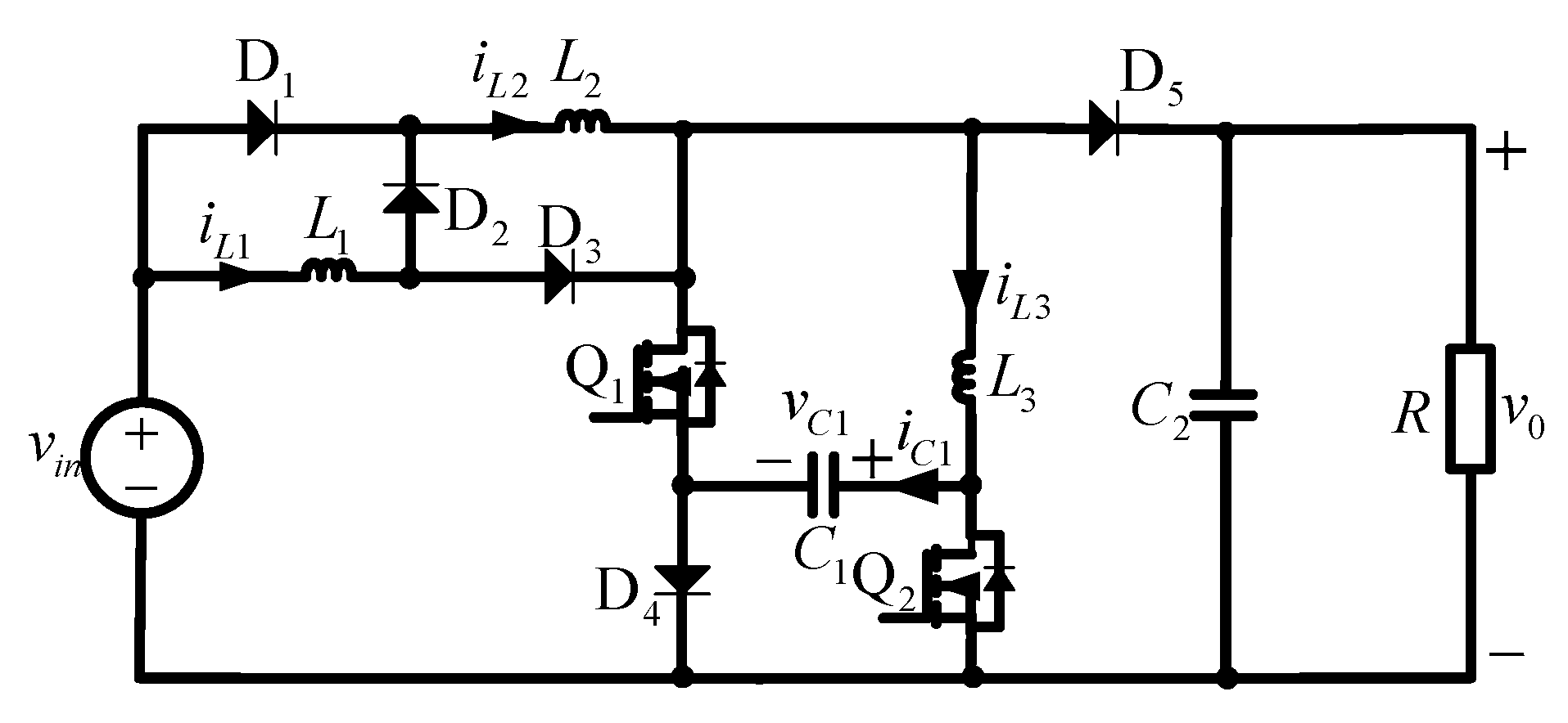
A circuit schematic of the proposed step-up converter is shown in Figure 1. It consists of two power switches (Q1 and Q2), five diodes (D1, D2, D3, D4, and D5), three inductors (L1, L2, and L3), two capacitors (C1 and C2), and the resistive load R. Two power switches conduct synchronically and are driven by the same PWM signal vd, with the period being T and duty cycle being d. The currents through the three inductors are denoted by iL1, iL2 and iL3. The voltages across the two capacitors are defined as vC1 and v0. Notably, the proposed step-up converter operating in the continuous conduction mode (CCM) is the only concern here, and its possible stages are shown in Figure 2. Based on the relation between inductors L1 and L2, there are three cases for the proposed step-up converter, case 1: L1 = L2, case 2: L1 < L2 and case 3: L1 > L2. The principle of the proposed step-up converter under the three cases is discussed in detail in the following subsections.
2.1. Case 1: L1 = L2
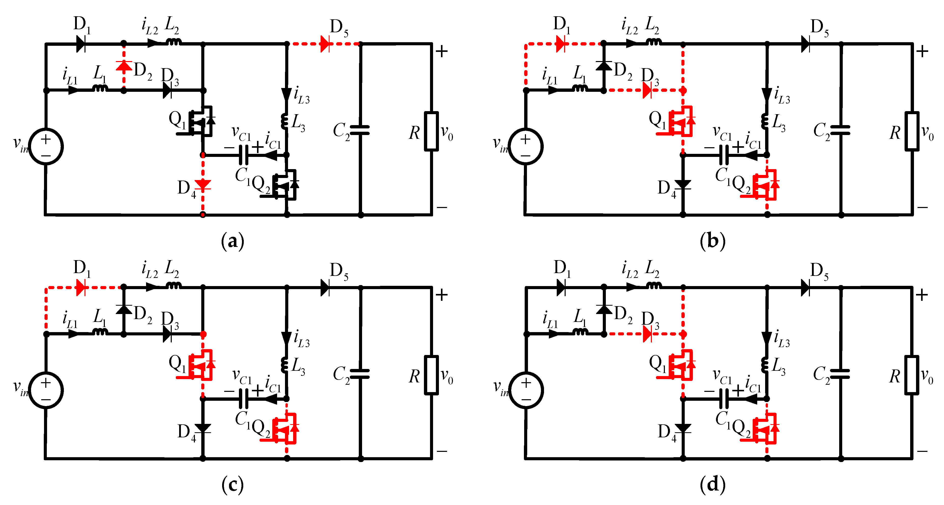
For this case, the proposed step-up converter has only two operation stages; their equivalent circuits are shown in Figure 2a,b.
2.1.1. Stage 1
Figure 2a shows that two power switches (Q1 and Q2) are turned on for the high level of PWM signal vd, and three of the diodes D2, D4 and D5 do not conduct for the inverse biased voltage, whereas two of the diodes (D1 and D3) conduct for the forward biased voltage. That is, the state of power switches and diodes is: (Q1, Q2, D1, D2, D3, D4, D5≡ON, ON, ON, OFF, ON, OFF, OFF) within NT < t ≤ NT + dT where N is a natural number. Accordingly, the input voltage source supplies the energy to two input inductors (L1 and L2) so that both of them are magnetized and their currents increase. Because L1 = L2, the currents through these two inductors are equal, that is, iL1 = iL2. Capacitor C1 is in parallel with inductor L3. Consequently, capacitor C1 is discharged so that its voltage decreases and inductor L3 is demagnetized so that its current also decreases. In addition, capacitor C2 delivers energy to the resistive load R. The associated equations for stage 1 are:
2.1.2. Stage 2
Figure 2b shows that two power switches (Q1 and Q2) are turned off for the low level of PWM signal vd. Three diodes (D2, D4, and D5) conduct, and the remaining diodes (D1 and D3) do not conduct. That is, the state of power switches and diodes is: (Q1, Q2, D1, D2, D3, D4, D5≡OFF, OFF, OFF, ON, OFF, ON, ON) within NT + dT < t ≤ NT + T. Hence, inductor L1 is in series with inductor L2, leading to iL1 = iL2, and together with the input voltage vin, they supply the energy to inductor L3 and capacitor C1. The corresponding equations for stage 2 are:
2.2. Case 2: L1 < L2
For case 2, besides stage 1 and stage 2, it has stage 3, as shown in Figure 2c, corresponding to (Q1, Q2, D1, D2, D3, D4, D5≡OFF, OFF, OFF, ON, ON, ON, ON) within NT + dT < t ≤ NT + dT + d11T because diode D3 is still conducting for iL1 > iL2. Its mathematical model is:
Notably, stage 3 will last until iL1 = iL2, leading to the diode D3 being off and the proposed step-up converter immediately operating in stage 2. Therefore, the sequence of operations of the proposed step-up converter in case 2 is: stage 1 (Figure 2a) during NT < t ≤ NT + dT, stage 3 (Figure 2c) during NT + dT < t ≤ NT + dT + d11T, and stage 2 (Figure 2b) during NT + dT + d11T < t ≤ NT + T.
2.3. Case 3: L1 > L2
For case 3, besides stage 1 and stage 2, it has stage 4, as shown in Figure 2d, corresponding to (Q1, Q2, D1, D2, D3, D4, D5≡OFF, OFF, ON, ON, OFF, ON, ON) during NT + dT < t ≤ NT + dT + d22T because diode D1 is still conducting for iL1 < iL2. Its equations are:
Please note that stage 4 will end if iL1=iL2, which prevents diode D1 from conducting and the proposed step-up converter will immediately operate in stage 2. Therefore, the sequence of operations of the proposed step-up converter in case 3 is: stage 1 (Figure 2a) during NT < t ≤ NT + dT, stage 4 (Figure 2d) during NT + dT < t ≤ NT + dT + d22T, and stage 2 (Figure 2b) during NT + dT + d22T < t ≤ NT + T.
3. Modeling and Theoretical Analysis
Based on the averaging method in [19], the averaged model for the proposed step-up converter under the three cases are established and analyzed. Firstly, some symbols are defined. x is defined as the variables of the proposed step-up converter, such as iL1, iL2, iL3, vC1, v0, d, and vin. 〈x〉, X and are denoted by their averaged, DC and small AC values, respectively. Also, the following items are assumed:
3.1. Averaged Model
3.1.1. Case 1: L1 = L2
For this case, L1 = L2 so that iL1 = iL2. From (1) and (2), and using the averaging method in [19], the averaged model of the proposed step-up converter in case 1 can be directly derived as follows:
3.1.2. Case 2: L1 < L2
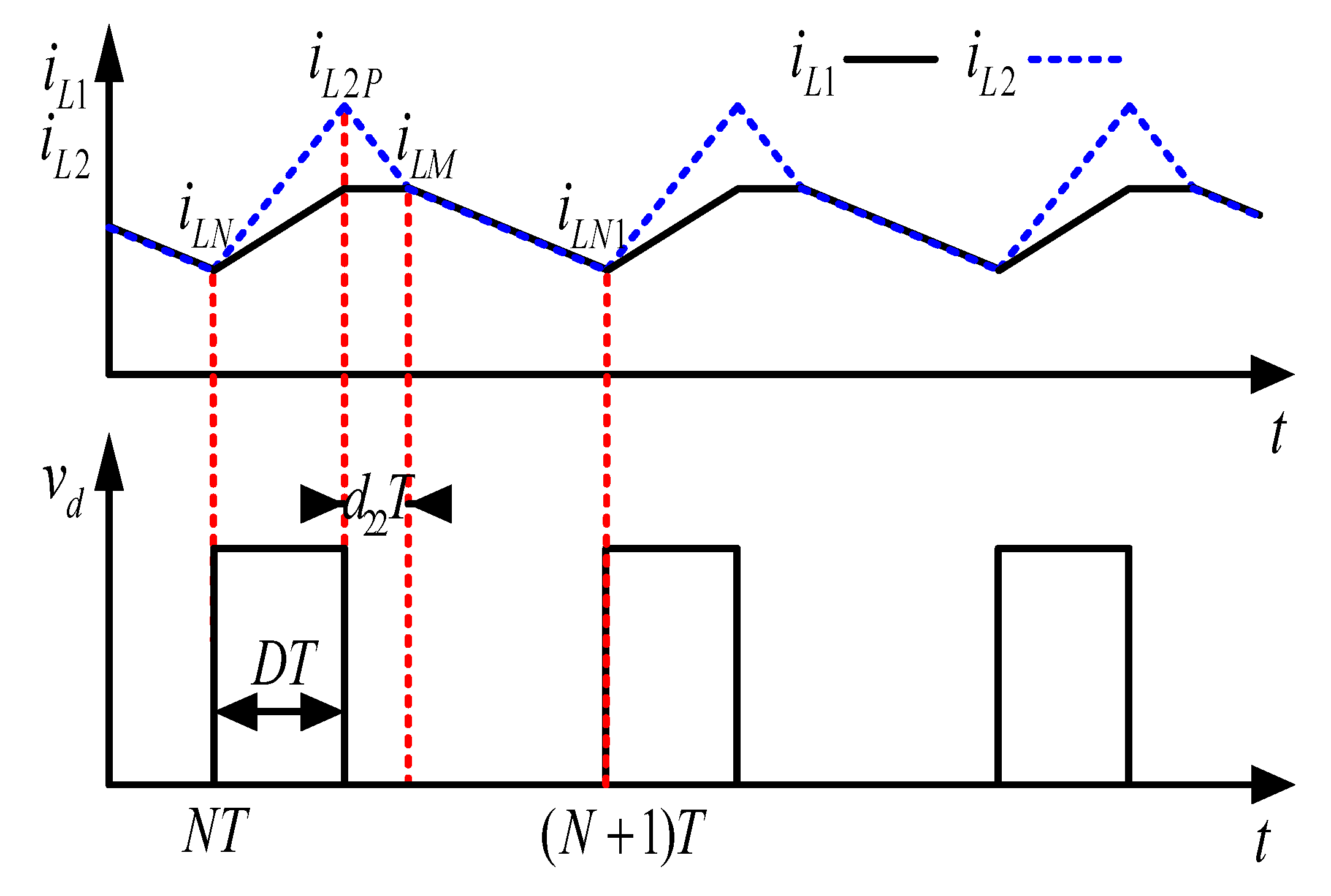
As described in Section 2, there are three stages of the proposed step-up converter in case 2. The typical time-domain waveforms for the inductor currents iL1 and iL2 and the PWM signal vd are plotted in Figure 3, where ILN, ILM, and ILN1 are the values of iL1 and iL2 at t = NT, t = (N + d + d11)T, and t = (N + 1)T, respectively, and IL1P is the value of iL1 at t = (N + d + d11)T.
Based on (1), (2), (3), and Figure 3 and using the geometrical technique, the following equations can be derived:
Hence, the expressions for d11 and 〈iL2〉 can be derived as follows:
where K = 1/L1 − 1/L2. Thereby, the completed averaged model of the proposed step-up converter in case 2 can be obtained by using the averaging method in (1)–(3), and then combining (10) and (11). The result is:
3.1.3. Case 3: L1 > L2
As indicated in Section 2, for case 3, the proposed step-up converter also has three stages, and its typical domain waveforms are shown in Figure 4, where ILN, ILM, and ILN1 are the values of iL1 and iL2 at t = NT, t = (N + d + d22)T and t = (N + 1)T, respectively, and IL2P is the value of iL2 at t = (N + d + d22)T. Because case 3 is similar to case 2, the completed averaged model of the proposed step-up converter for case 3 is directly derived as follows:
3.2. DC Equilibrium Point
By substituting (5) into (6), (12), and (13), and then separating DC items, the DC equilibrium points of the proposed step-up converter under three cases can be derived; they are shown in Table 1.
From Table 1, it can be seen that the expressions for the DC voltage V0 under the three cases are equal. In other words, no matter what the relation between L1 and L2 is, the voltage conversion ratio M of the proposed step-up converter can be described as follows:
Also, the expressions for the DC voltage VC1 under three cases are also equal. In conclusion, the relation between L1 and L2 does not influence V0 and VC1.
3.3. Voltage Stress of Power Switches and Diodes under Three Cases
Based on the definition of the voltage stress on the power switch and diode, the corresponding results for the proposed step-up converter under the three cases can be derived; they are shown in Table 2. One can see that the voltage stresses on the power switches (Q1 and Q2) and diodes (D2, D4 and D5) under the three cases are equal except for the diodes D1 and D3.
3.4. Ripples for Inductor Currents and Capacitor Voltages
The ripples for the inductor currents and the capacitor voltages can be obtained by using (1) and Table 1. The results are shown in Table 3.
Hence, unlike the voltage ripple for capacitor C1, the current ripples for inductors (L1, L2 and L3) and the voltage ripples for capacitor C2 under the three cases are equal. Generally, the ripple ratio, which is defined by the ripple over the corresponding DC value, can be used to select the values of the inductors and capacitors.
3.5. Transfer Functions
The transfer function is fundamental for the consequent controller design for DC-DC converters. By substituting (5) into (6), (12), and (13), and then separating AC items and ignoring the second- and higher-order AC terms because their values are very small, the corresponding transfer functions for the proposed step-up converter under the three cases can be derived by using their respective definitions.
The control-to-output voltage transfer function Gvd(s), the input voltage-to-output voltage transfer function Gvv(s), the control-to-inductor current iL1 transfer function Gi1d(s), and the input voltage-to-inductor current iL1 transfer function Gi1v(s) of the proposed step-up converter can be obtained as follows:
where the expressions for A, Bd and Bv under the three cases are presented in Table 4.
4. Comparisons among Different Topologies
Table 5 shows the comparisons among the modified Sheppard-Taylor converter (MSTC) in [14], the PWM Z-source DC-DC converter (ZSC) in [18], the simple modified Sheppard-Taylor converter (SMSTC) in [15], and the proposed step-up converter (PSUC).
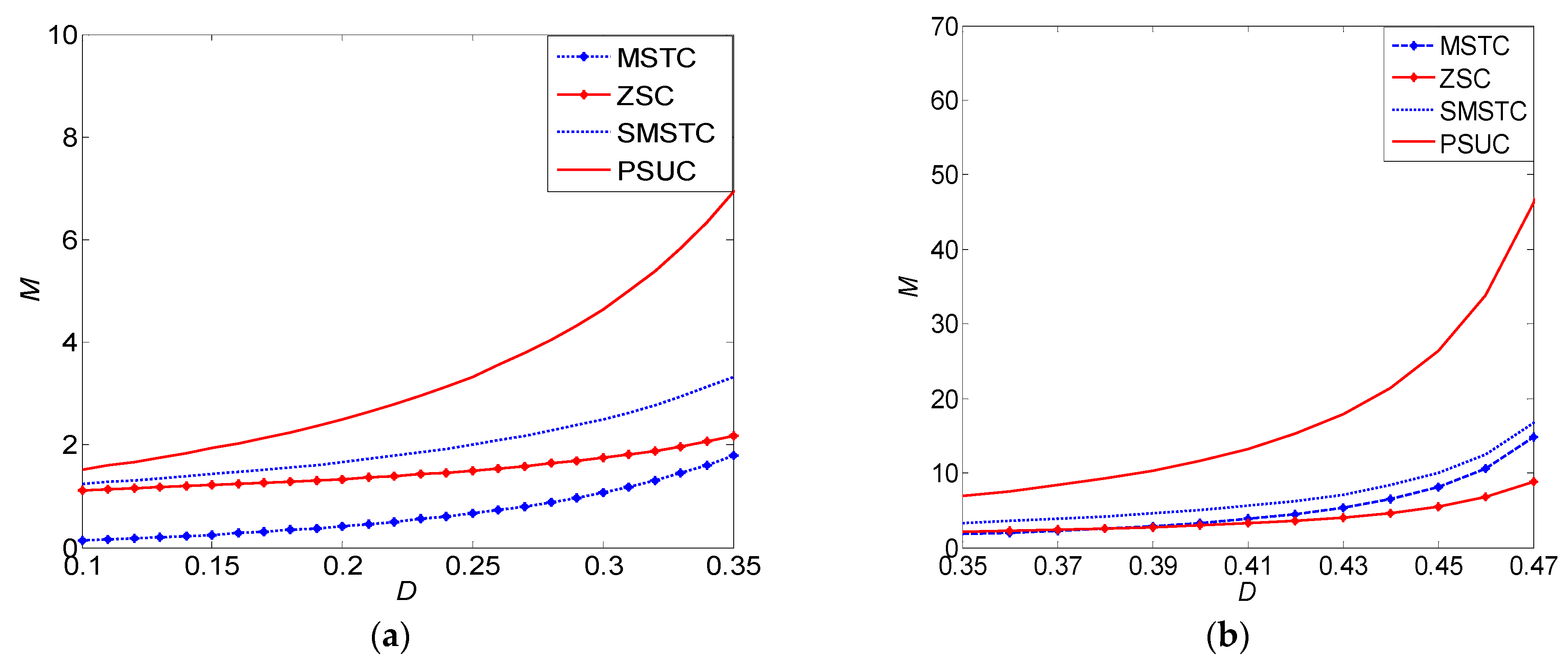
Although the proposed step-up converter has five diodes, while others have less, from Figure 5, which shows the comparisons of the voltage conversion ratio M among these converters under different duty cycle D, it can be seen that the proposed step-up converter possesses the highest voltage conversion ratio. For example, the voltage conversion ratio M of the proposed step-up converter is up to 46.224 at D = 0.47. Additionally, the ZSC’s output voltage is floating, whereas those of the others are not.
5. Saber Simulations and Circuit Experiments
For validation purposes, the circuit for the proposed step-up converter is designed. The given specifications are described as Vin = 12 V, V0 = 90 V, f = 32 kHz, R = 300 Ω. Thus, from (14), the duty cycle D should be equal to 0.358742. Based on the voltage stresses of the power switches and diodes in Table 2, the HEXFET Power MOSFET IRFP4668 whose VDSS = 200 V was selected for power switches Q1 and Q2, and the Switchmode Schotty Power Rectifier MBR40250 rated for 250 V was selected for diodes D1, D2, D3, D4, and D5. Inductors (L1, L2 and L3) can be designed by using their current ripple ratios εL = ΔiL/IL whose values should generally be less than 45%. Capacitors C1 and C2 can be designed by using their voltage ripple ratios εC = ΔvC/VC whose values should be less than 20% and 0.5%, respectively. Thereby, from Table 1 and Table 3, the current ripple ratio for each inductor and the voltage ripple ratio for each capacitor under each case can be calculated, and accordingly the selected inductors and capacitors in each case should satisfy conditions: L1 > 1048 µH, L2 > 1048 µH, L3 > 1210 µH, C1 > 2.06 µF and C2 > 7.47 µF. Here, C1 = 4.7 μF with rC1 = 10 mΩ, C2 = 40 μF with rC2 = 6 mΩ, and L3 = 2.76 mH with rL3 = 164 mΩ were selected for the proposed step-up converter. Additionally, L1 = L2 = 1.2 mH with rL1 = rL2 = 70 mΩ were selected for case 1, L1 = 1.2 mH with rL1 = 70 mΩ and L2 = 2.27 mH with rL2 = 156 mΩ were selected for case 2, and L1 = 2.27 mH with rL1 = 156 mΩ and L2 = 1.2 mH with rL2 = 70 mΩ were selected for case 3.
From the above-designed circuit parameters, the simulated model in Saber software, which is widely used in the field of power electronics [20], for the proposed step-up converter is constructed, and some measured results on the output voltage V0 from the saber simulations were presented in Table 6. One can see that the output voltages V0 for the proposed step-up converter in the three cases were close, and their values were smaller than the required 90 V because the parasitic parameters were considered in the Saber simulations.
Moreover, a hardware circuit for the proposed step-up converter with the same circuit parameters and selected power switches and diodes was also constructed. Notably, in the experiments, the photocoupler TLP250H was applied to drive the power switches. The averaged values of the input voltage Vin, the input current Iin and the output voltage V0 with different duty cycle D for the proposed step-up converter under case 1 were measured. In addition, then, the voltage conversion ratio M = V0/Vin and the efficiency η = V02/(RVinIin) with different duty cycle D for the proposed step-up converter in case 1 were calculated and plotted in Figure 6a,b, respectively. Simultaneously, the corresponding Saber simulations were also detected, calculated, and plotted in Figure 6a,b. It can be seen that the experimental results were in basic agreement with the Saber simulations.
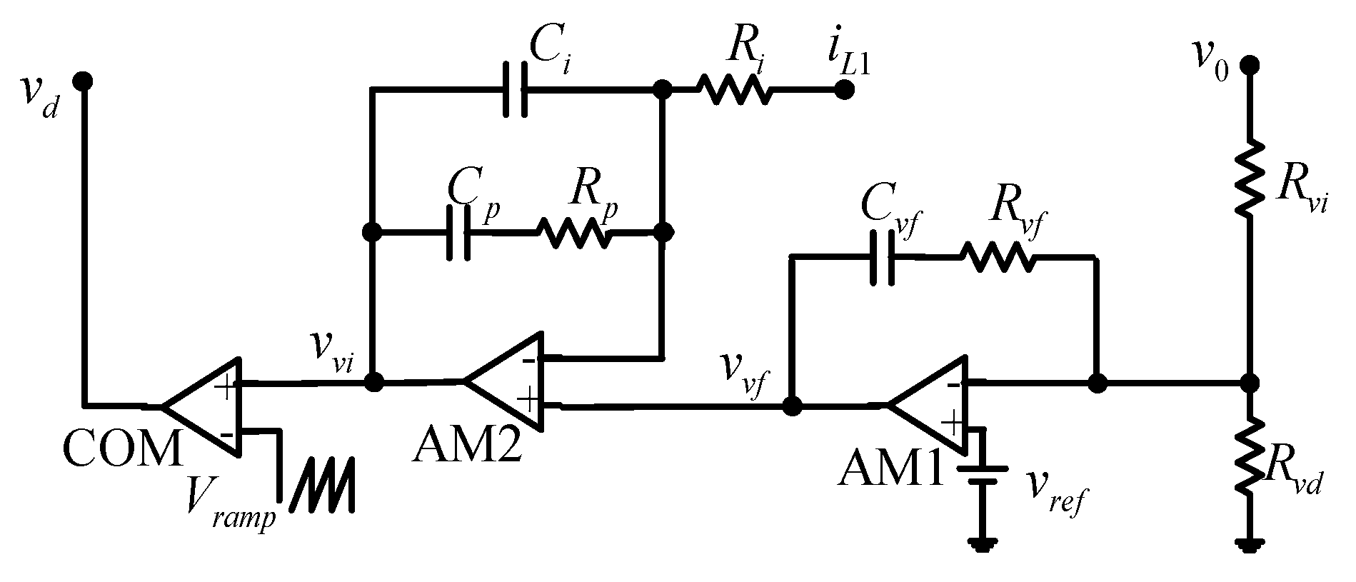
As shown in Table 6, it is necessary to design an appropriate controller for this proposed step-up converter. Based on the circuit parameters, the zeros of Gvd(s) (shown in (15)) can be calculated. The results showed that Gvd(s) was a fourth-order and non-minimum phase since it had right-half side zeros, so that it was difficult to select only the single voltage loop to obtain good performance [21]. Alternatively, an average current mode controller shown in Figure 7 was selected and designed for the proposed step-up converter. This controller had an outer voltage loop and an inner current loop. For the outer voltage loop, it was necessary to detect the output voltage v0 and design a voltage compensator. For the inner current loop, it was necessary to select one of the inductor currents in the proposed step-up converter and design a current compensator. Due to all the Gi1d(s)’s poles and zeros being in the left-half side of the s-plane, that is, Gi1d(s) is stable and minimum phase, the inductor current iL1 was selected and measured for the average current mode controller. Notably, the inductor current iL1 here was transformed into a voltage with the same value through the current transducer LA55-A. The current compensator’s output voltage is denoted by vvi. AM1 and AM2 were realized by the operational amplifiers LF356 and COM was realized by the voltage comparator LM311. The corresponding parameters were: Rvi = 1000 kΩ, Rvd =20 kΩ, Rvf = 200 kΩ, Cvf = 10 nF, Ri = 20 kΩ, Rp = 180 kΩ, Cp = 10 nF, Ci = 100 pF, Vref = 1.76 V. The PWM signal vd was generated by comparing the voltage vvi with the ramp signal Vramp, whose expression was given as follows:
where VL = 0 V, VU = 10 V and T = 1/f.
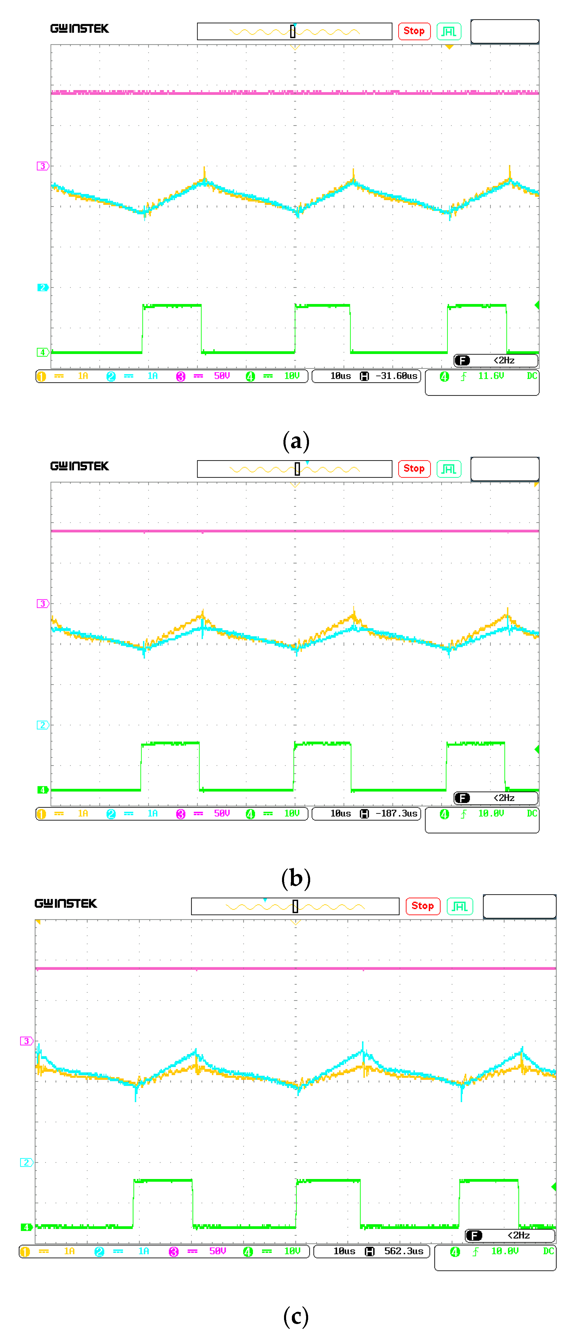
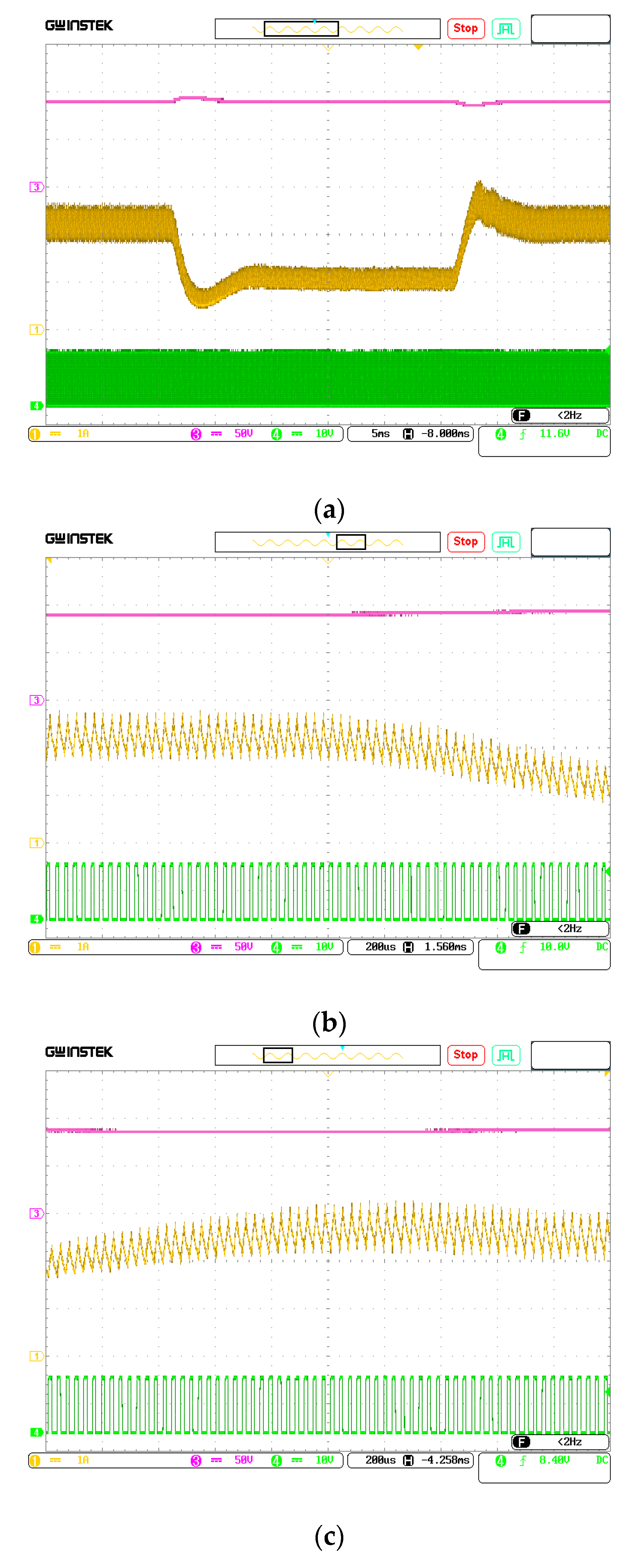
The experimental results for the output voltage v0, the inductor currents iL1 and iL2, and the PWM signal vd for the average-current mode controlled proposed step-up converter under the three cases are presented in Figure 8a–c, respectively. One can see that the output voltages v0 for the systems under the three cases are really the same, despite different relations between the inductors L1 and L2. Moreover, the response of the output voltage v0, the inductor current iL1, and the PWM signal vd for the average-current mode controlled proposed step-up converter with the step changing of the load R being 300 Ω–600 Ω–300 Ω is shown in Figure 9. One can see that the closed-loop controlled proposed step-up converter had good performance.
6. Conclusions
This paper introduces a new step-up converter. The results from theoretical analysis, the Saber simulations, and the circuit experiments show that, even if it has five diodes and five storage elements, it still has the following five good features:
- (1)
- Although this new step-up converter has five storage elements, that is, three inductors and two capacitors, its averaged model is still fourth-order, because one of the input inductor currents can be expressed by another input inductor current.
- (2)
- The relation between the inductor L1 and L2 has three cases: L1 = L2, L1 < L2, and L1 > L2. However, these relations do not influence its output voltage V0, i.e., the output voltage V0 are the same in the three cases.
- (3)
- Compared to MSTC, ZSC, and SMSTC, the proposed step-up converter has ultrahigh voltage conversion ratio.
- (4)
- The output voltage of the proposed step-up converter is common-ground and common-polarity with its input voltage, so its value is easy to detect.
- (5)
- The proposed step-up converter has no abrupt changes in capacitor voltage and inductor current, so it does not suffer from infinite capacitor current and inductor voltage.
Thus, the proposed step-up converter with ultrahigh voltage conversion ratio is a good candidate topology for applications of photovoltaic systems and fuel cell systems, and these applications will be investigated in future work.
Nomenclature of Main Symbols and Variables
| Q1, Q2 | Power mosfets |
| D1, D2, D3, D4, D5 | Power Diodes |
| L1, L2, L3 (mH) | Inductors of power stage |
| C1, C2 (μF) | Capacitors of power stage |
| R (Ω) | Resistive load |
| Vramp | Ramp signal |
| vd (V) | PWM signal |
| f (kHz) | Switching frequency |
| d, D, | Instantaneous, DC and small signal of duty cycle |
| vin, Vin, (V) | Instantaneous, DC and small signal of input voltage |
| T (μs) | Switching period |
| iL1, iL2, iL3 (A) | Instantaneous values of inductor currents |
| IL1, IL2, IL3 (A) | DC values of inductor currents |
| 〈iL1〉, 〈iL2〉, 〈iL3〉 (A) | Averaged values of inductor currents |
| , (A) | Small signal of inductor currents |
| ΔiL1, ΔiL2, ΔiL3 (A) | Ripples of inductor currents |
| vC1, v0 (V) | Instantaneous values of capacitor voltage of C1, C2 |
| 〈vC1〉, 〈v0 〉 (V) | Averaged values of capacitor voltage of C1, C2 |
| VC1, V0 (V) | DC values of capacitor voltage of C1, C2 |
| , (V) | Small signal of capacitor voltage of C1, C2 |
| ΔvC1, Δv0 (V) | Ripples of capacitor voltage of C1, C2 |
| Gvd(s) | Control-to-output voltage transfer function |
| Gvv(s) | Input voltage-to-output voltage transfer function |
| Gi1d(s) | Control-to-inductor current iL1 transfer function |
| Gi1v(s) | Input voltage-to-inductor current iL1 transfer function |
| Rvi, Rvd, Rvf, Ri, Rp (kΩ) | Resistors of average current mode controller |
| Cvf, Cp, Ci (μF) | Capacitors of average current mode controller |
| Vref (V) | Reference voltage |
| VL, VU (V) | Lower and upper threshold of ramp signal |
Author Contributions
F.W. conceived, validated and wrote the manuscript. H.H.-C.I. and J.L. revised the manuscript. All authors contributed to the manuscript.
Funding
This research was funded by the National Natural Science Foundation of China (grant nos. 51377124 and 51521065), the China Scholarship Council (grant no. 201706285022), a Foundation for the Author of National Excellent Doctoral Dissertation of PR China (grant no. 201337), and the New Star of Youth Science and Technology of Shaanxi Province (grant no. 2016KJXX-40).
Conflicts of Interest
The authors declare no conflict of interest.
References
- Hwu, K.I.; Jiang, W.Z.; Chien, J.Y. Isolated high voltage-boosting converter derived from forward converter. Int. J. Circuit Theory Appl. 2016, 44, 280–304. [Google Scholar] [CrossRef]
- Tang, Y.; Wang, T.; He, Y.H. A switched-capacitor-based active-network converter with high voltage gain. IEEE Trans. Power Electron. 2014, 29, 2959–2968. [Google Scholar] [CrossRef]
- Ben-Yaakov, S.; Zeltser, I. The dynamics of a PWM Boost converter with resistive input. IEEE Trans. Ind. Eletron. 1999, 46, 613–619. [Google Scholar] [CrossRef]
- Yang, L.S.; Liang, T.J.; Chen, J.F. Transformerless DC-DC converters with high step-up voltage gain. IEEE Trans. Ind. Eletron. 2009, 56, 3144–3152. [Google Scholar] [CrossRef]
- Gules, R.; Santos, W.M.D.; Reis, F.A.D.; Romaneli, E.F.R.; Badin, A.A. A modified SEPIC converter with high static gain for renewable applications. IEEE Trans. Power Electron. 2014, 29, 5860–5871. [Google Scholar] [CrossRef]
- Mummadi, V.; Mohan, B.K. Robust digital voltage-mode controller for fifth-order Boost converter. IEEE Trans. Ind. Eletron. 2011, 58, 263–277. [Google Scholar] [CrossRef]
- Hwu, K.I.; Yau, Y.T. A KY Boost converter. IEEE Trans. Power Electron. 2010, 25, 2699–2703. [Google Scholar] [CrossRef]
- Hwu, K.I.; Huang, K.W.; Tu, W.C. Step-up converter combining KY and buck-boost converters. Electron. Lett. 2011, 47, 722–724. [Google Scholar] [CrossRef]
- Luo, F.L.; Ye, H. Positive output super-lift converters. IEEE Trans. Power Electron. 2003, 18, 105–113. [Google Scholar]
- Hwu, K.I.; Yau, Y.T. High step-up converter based on charge pump and Boost converter. IEEE Trans. Power Electron. 2012, 27, 2484–2494. [Google Scholar] [CrossRef]
- Al-Saffar, M.A.; Ismail, E.H. A high voltage ratio and low stress DC-DC converter with reduced input current ripple for fuel cell source. Renew. Energy 2015, 82, 35–43. [Google Scholar] [CrossRef]
- Hwu, K.I.; Chuang, C.F.; Tu, W.C. High voltage-boosting converters based on bootstrap capacitors and boost inductors. IEEE Trans. Ind. Eletron. 2013, 60, 2178–2193. [Google Scholar] [CrossRef]
- Chen, Y.T.; Lin, W.C.; Liang, R.H. An interleaved high step-up DC-DC converter with double boost paths. Int. J. Circuit Theory Appl. 2015, 43, 967–983. [Google Scholar] [CrossRef]
- Kanaan, H.Y.; Al-Haddad, K.; Hayek, A.; Mougharbel, I. Design, study, modelling and control of a new single-phase high power factor rectifier based on the single-ended primary inductance converter and the Sheppard-Taylor topology. IET Power Electron. 2009, 2, 163–177. [Google Scholar] [CrossRef]
- Hua, C.C.; Chiang, H.C.; Chuang, C.W. New boost converter based on Sheppard-Taylor topology. IET Power Electron. 2014, 7, 167–176. [Google Scholar] [CrossRef]
- Wang, F.Q. Improved transfer functions for modified sheppard-taylor converter that operates in CCM: Modeling and application. J. Power Electron. 2017, 17, 884–891. [Google Scholar]
- Patidar, K.; Umarikar, A.C. A step-up PWM DC-DC converter for renewable energy applications. Int. J. Circuit Theory Appl. 2016, 44, 817–832. [Google Scholar] [CrossRef]
- Galigekere, V.P.; Kazimierczuk, M.K. Analysis of PWM Z-Source DC-DC Converter in CCM for Steady State. IEEE Trans. Circuits Syst. I Regul. Pap. 2012, 59, 854–863. [Google Scholar] [CrossRef]
- Middlebrook, R.D.; Cuk, S. A general unified approach to modelling switching-converter power stages. Int. J. Electron. 1977, 42, 521–550. [Google Scholar] [CrossRef]
- Shi, J.J.; Liu, T.J.; Cheng, J.; He, X.N. Automatic current sharing of an input-parallel output-parallel (IPOP)-connected DC-DC converter system with chain-connected rectifiers. IEEE Trans. Power Electron. 2015, 30, 2997–3016. [Google Scholar] [CrossRef]
- Morales-Saldana, J.A.; Galarza-Quirino, R.; Leyva-Ramos, J.; Carbajal-Gutierrez, E.E.; Ortiz-Lopez, M.G. Multiloop controller design for a quadratic boost converter. IET Electr. Power Appl. 2007, 1, 362–367. [Google Scholar] [CrossRef]
Figure 1.
Circuit schematic of the proposed step-up converter.

Figure 2.
Equivalent circuits for possible stages of the proposed step-up converter in CCM. (a) Stage 1; (b) Stage 2; (c) Stage 3; (d) Stage 4.
Figure 2.
Equivalent circuits for possible stages of the proposed step-up converter in CCM. (a) Stage 1; (b) Stage 2; (c) Stage 3; (d) Stage 4.

Figure 3.
Typical time-domain waveforms about iL1, iL2 and vd for the proposed step-up converter under L1 < L2.
Figure 3.
Typical time-domain waveforms about iL1, iL2 and vd for the proposed step-up converter under L1 < L2.

Figure 4.
Typical time-domain waveforms about iL1, iL2 and vd for the proposed step-up converter under L1 > L2.
Figure 4.
Typical time-domain waveforms about iL1, iL2 and vd for the proposed step-up converter under L1 > L2.

Figure 5.
Comparisons about the voltage conversion ratio M among MSTC, ZSC, SMSTC and PSUC. (a) D is within 0.1–0.35; (b) D is within 0.35–0.47.
Figure 5.
Comparisons about the voltage conversion ratio M among MSTC, ZSC, SMSTC and PSUC. (a) D is within 0.1–0.35; (b) D is within 0.35–0.47.

Figure 6.
The Saber simulations and the experiments about the voltage conversion ratio M and the efficiency for the proposed step-up converter under case 1. (a) The voltage conversion ratio M; (b) The efficiency.
Figure 6.
The Saber simulations and the experiments about the voltage conversion ratio M and the efficiency for the proposed step-up converter under case 1. (a) The voltage conversion ratio M; (b) The efficiency.

Figure 7.
Circuit schematic for the average current mode controller.

Figure 8.
Experimental results for v0 (Top: 50 V/div, Pink), iL1 (Middle: 1 A/div, Yellow), iL2 (Middle: 1 A/div, Blue) and vd (Bottom: 10 V/div, Green) for the average current mode controlled proposed step-up converter under three cases. (a) Case 1: L1 = 1.2 mH and L2 = 1.2 mH; (b) Case 2: L1 = 1.2 mH and L2 = 2.27 mH; (c) Case 3: L1 = 2.27 mH and L2 = 1.2 mH.

Figure 9.
Response of v0 (Top: 50 V/div, Pink), iL1 (Middle: 1 A/div, Yellow) and vd (Bottom: 10 V/div, Green) with the step change of the resistive load R being 300 Ω–600 Ω–300 Ω. (a) Time: 5 ms/div; (b) Close-up view of response for the step changing of the resistive load R being 300 Ω–600 Ω, Time: 200 µs/div; (c) Close-up view of response for the step changing of the load R being 600 Ω–300 Ω, Time: 200 µs/div.


Table 1.
DC equilibrium points of proposed step-up converter.
| Items | Case 1: L1 = L2 | Case 2: L1 < L2 | Case 3: L1 > L2 |
|---|---|---|---|
| IL1 | |||
| IL2 | |||
| IL3 | |||
| VC1 | |||
| V0 |
where IL0 = KD2Vin/(4f(1 − 2D)2), K1 = (D − 2)((D − 1)L1/L2 + 1 + D), K2 = K1 − (2D + L1K(1 − D))(2 − D)(1 − 2D)/D, K3 = (D − 2) ((D − 1) L2/L1 + 1 + D), K4 = K3 − (2D − L2K(1 − D))(2 − D)(1 − 2D)/D.
Table 2.
Voltage stress on power switches and diodes.
| Items | Case 1: L1 = L2 | Case 2: L1 < L2 | Case 3: L1 > L2 |
|---|---|---|---|
| Q1 | |||
| Q2 | |||
| D1 | |||
| D2 | |||
| D3 | |||
| D4 | |||
| D5 |
Table 3.
Ripples for inductor currents and capacitor voltages.
| Items | Case 1: L1 = L2 | Case 2: L1 < L2 | Case 3: L1 > L2 |
|---|---|---|---|
| ΔiL1 | |||
| ΔiL2 | |||
| ΔiL3 | |||
| ΔvC1 | |||
| Δv0 |
Table 4.
Expressions for A, Bd and Bv for the proposed step-up converter.
| Case | A | Bd | Bv |
|---|---|---|---|
| Case 1: L1 = L2= L | |||
| Case 2: L1 < L2 | |||
| Case 3: L1 > L2 |
where α2 = KD3(1 − M − 2L1K(1 + M − MD))/(2f(1 − M)), α3 = − KD3 (1 − M + 2L2K(1 + M − MD))/(2f(1 − M)), β2 = − 2M2Vin/ (R(1 + D)) − 2K1IL0 + 3D2KVin(1 + M(1 − D))(1 − L1K (1 + M(1 − D))/(1 − M))/(2f), β3 = − 2M2Vin/(R (1 + D)) + 2K3IL0 − 3D2KVin (1 + M(1 − D))(1 + L2K(1 + M(1 − D))/ (1 − M))/(2f), β4 = (2(1 + M(1 − D))(1 − M) − (1 + M)2)/(1 − M)2.
Table 5.
Comparisons among the converters.
| Topology | MSTC in [14] | ZSC in [18] | SMSTC in [15] | PSUC |
|---|---|---|---|---|
| M | ||||
| Switches | 2 | 1 | 2 | 2 |
| Diodes | 4 | 1 | 3 | 5 |
| Inductors | 2 | 3 | 1 | 3 |
| Capacitors | 2 | 3 | 2 | 2 |
| Output floating | No | Yes | No | No |
Table 6.
Comparisons of the output voltage V0 between the calculations and the saber simulations.
| Cases | L1 = L2 | L1 < L2 | L1 > L2 |
|---|---|---|---|
| Calculations for V0 | 90.000 V | 90.000 V | 90.000 V |
| Simulations for V0 | 84.217 V | 83.362 V | 83.363 V |
© 2018 by the authors. Licensee MDPI, Basel, Switzerland. This article is an open access article distributed under the terms and conditions of the Creative Commons Attribution (CC BY) license (http://creativecommons.org/licenses/by/4.0/).
Share and Cite
MDPI and ACS Style
Wang, F.; Iu, H.H.-C.; Li, J. A Novel Step-Up Converter with an Ultrahigh Voltage Conversion Ratio. Energies 2018, 11, 2693. https://doi.org/10.3390/en11102693
AMA Style
Wang F, Iu HH-C, Li J. A Novel Step-Up Converter with an Ultrahigh Voltage Conversion Ratio. Energies. 2018; 11(10):2693. https://doi.org/10.3390/en11102693
Chicago/Turabian StyleWang, Faqiang, Herbert Ho-Ching Iu, and Jing Li. 2018. "A Novel Step-Up Converter with an Ultrahigh Voltage Conversion Ratio" Energies 11, no. 10: 2693. https://doi.org/10.3390/en11102693
Note that from the first issue of 2016, this journal uses article numbers instead of page numbers. See further details here.