A Low-Noise Chopper Amplifier with Offset and Low-Frequency Noise Compensation DC Servo Loop

1
Institute of RF- & OE-ICs, School of Information and Engineering, Southeast University, Nanjing 210096, China
2
Engineering Research Center of RF-ICs & RF-Systems, Ministry of Education, Nanjing 210096, China
*
Authors to whom correspondence should be addressed.
†
Yuekai Liu and Zhijun Zhou contributed equally to this article.
Electronics 2020, 9(11), 1797; https://doi.org/10.3390/electronics9111797
Submission received: 11 October 2020
/
Revised: 23 October 2020
/
Accepted: 27 October 2020
/
Published: 29 October 2020
(This article belongs to the Section Circuit and Signal Processing)
Abstract
:The low-frequency and low-amplitude characteristics of neural signals poses challenges to neural signals recording. A low noise amplifier (LNA) plays an important role in the recording front-end. A chopper-stabilized analog front-end amplifier (FEA) for neural signal acquisition is presented in this paper. It solves the noise and offset interference caused by the servo loop in the chopper amplifier structure. The proposed FEA employs a switched-capacitor (SC) integrator with offset and low-frequency noise compensation. Moreover, a dc-blocking impedance is placed for ripple-rejection (RR), and a positive feedback loop is employed to increase input impedance. The proposed circuit is design in a 0.18-µm 1.8-V CMOS process. It achieves a bandwidth of up to 9 kHz for local field potential and action potential signals acquisition. The referred-to-input (RTI) noise is 0.72 µVrms in the 1 Hz~200 Hz frequency band and 3.46 µVrms in the 200 Hz~5 kHz frequency band. The noise effect factor is 0.43 (1 Hz~200 Hz) and 2.08 (200 Hz~5 kHz). CMRR higher than 87 dB and PSRR higher than 85 dB are achieved in the entire pass-band. It consumes a power of 3.96 µW/channel and occupies an area of 0.244 mm2/channel.
1. Introduction
High-density detection of neural signals has been a crucial step in emerging neurotherapy and physiology health recordings. Neural signals, such as local field potential (LFP), action potential (AP), electrocorticogram (ECoG), and electroencephalogram (EEG), have a weak amplitude ranging from tens of µV to a few mV and a frequency range below 5 kHz [1]. Neural signals are susceptible to the low-frequency noise of the detection devices and the front-end circuit. Generally, there will simultaneously exist a large electrode dc offset of tens of mV during the detection which needs to be suppressed by the recording front end. An analog front-end amplifier (FEA) is needed for neural signal detection and pre-procession before converting it to digital signals for further processing. Such a special application scenario puts forward particular requirements for the performance parameters of the FEA including low in-band noise and low dc offset. Moreover, integrated neural amplifier ICs need to consume minimal power (≤0.4 mW/mm2) and area for wearable and implantable biomedical applications [2,3].
The chopper-stabilized instrument amplifier structure using frequency modulation technique to avoid the interference of the low-frequency noise is widely used [4,5,6,7]. However, chopping used in an amplifier will arise other problems, such as the interference of the electrode dc offset. The dc servo loop solves such issue by forming a precise sub-Hz high-pass filtering to attenuate input dc offset, while occupying a small chip area. However, servo loop will bring in extra noise and dc offset, which degrade neural signal detection within the same frequency band.
Current publications provided several techniques to mitigate the noise contribution while maintaining a high accuracy of the high-pass corner frequency [8,9,10]. However, there are still some drawbacks that need to be improved, such as employing an additional chopper structure to servo loop increases high-frequency glitch noise and parasitic capacitance [8]. Employing an additional noise-nonlinearity-cancelling loop significantly increases the complexity of circuit [9]. A switched-capacitor structure has advantages of accurate time constant and high voltage linearity, and it is also insensitive to temperature and process [6,11,12,13]. However, the switched-capacitor technique suffers from its poor noise performance due to its charge injection, clock feed-through, and parasitic resistance [14,15].
In order to obtain a low referred-to-input (RTI) noise, while maintaining a high-pass corner frequency accuracy and high linearity performance, this paper presents a new dc servo loop structure. It uses a very-large-time-constant (VLT) switched-capacitor (SC) integrator with offset and low-frequency noise compensation. It maintains the advantages of the SC structure while suppressing the noise and offset contribution. By using proposed chopper amplifier with noise-compensated SC integrator, the two main noise sources in FEA, the RTI noise of the first stage operational amplifier (op amp), and the RTI noise of the servo loop have been mitigated. The next section will give a detailed description and analysis of the proposed VLT integrator with offset and low-frequency noise compensation and the structure of the capacitively-coupled chopper instrument amplifier in detail.
2. Design and Analysis of the Proposed Structure
2.1. VLT Switched-Capacitor Integrator with Offset and Low-Frequency Noise Compensation
Switched-capacitor integrator circuit is composed of standard CMOS switches, capacitors, and an op amp. The traditional SC integrator is shown in Figure 1a. Its bandwidth can be given by
where fcVLT is the switching clock frequency in SC integrator. It requires large capacitances to achieve a low unit-gain bandwidth. RTI dc offset of op amp VOS will be integrated to form a large output offset voltage. Its performance is also limited by the finite open-loop gain of op amp.
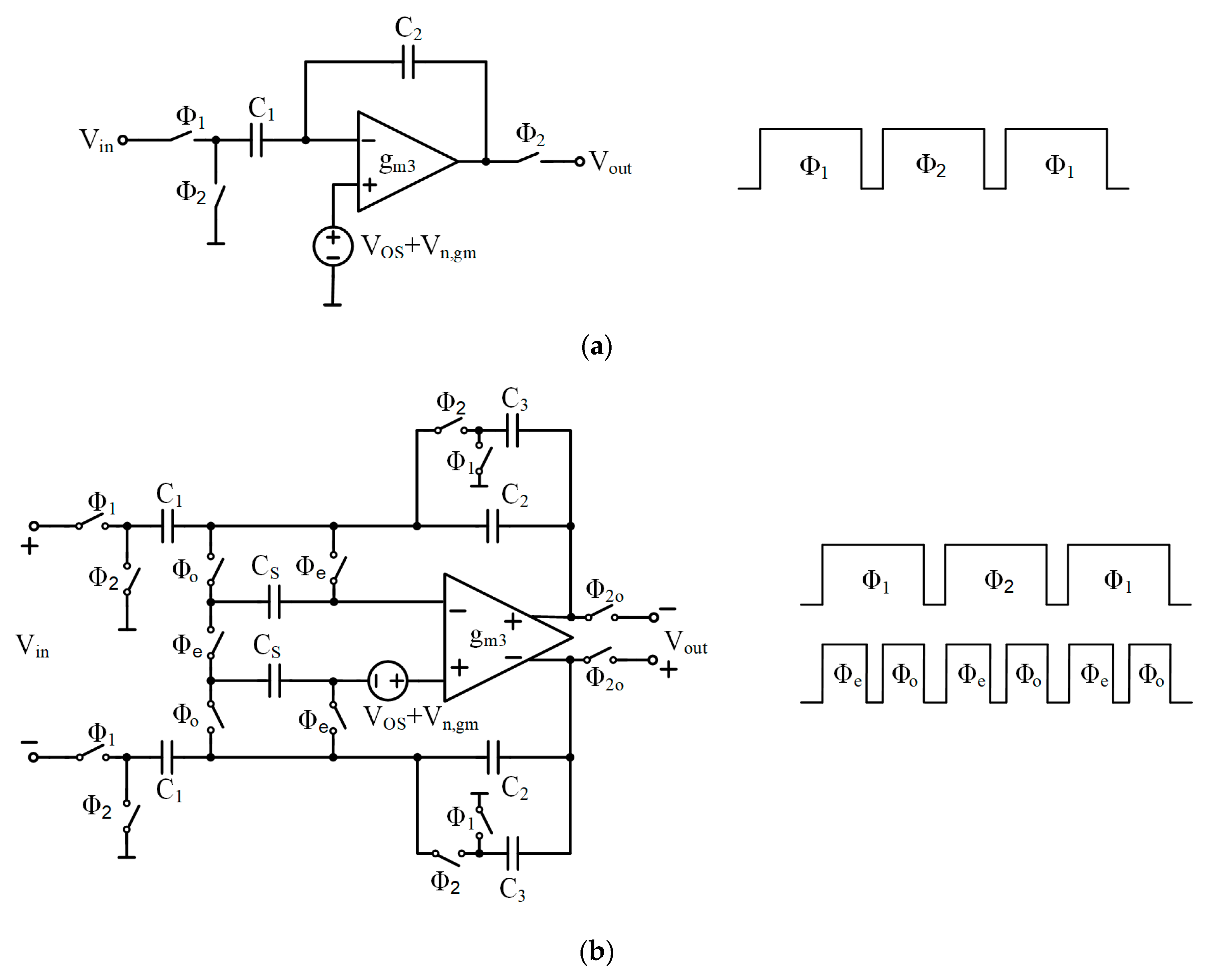
Figure 1b depicts the proposed fully differential VLT SC integrator with offset and low-frequency noise compensation. The circuit contains three capacitors (C1, C2, C3) and switches to realize VLT integrator in a more area-efficient way. Capacitor CS stores low-frequency noise Vn,gm and offset voltage VOS of op amp to compensate at input. The clock signal that controls the switches has four different phases, including 1e, 1o, 2e, 2o.
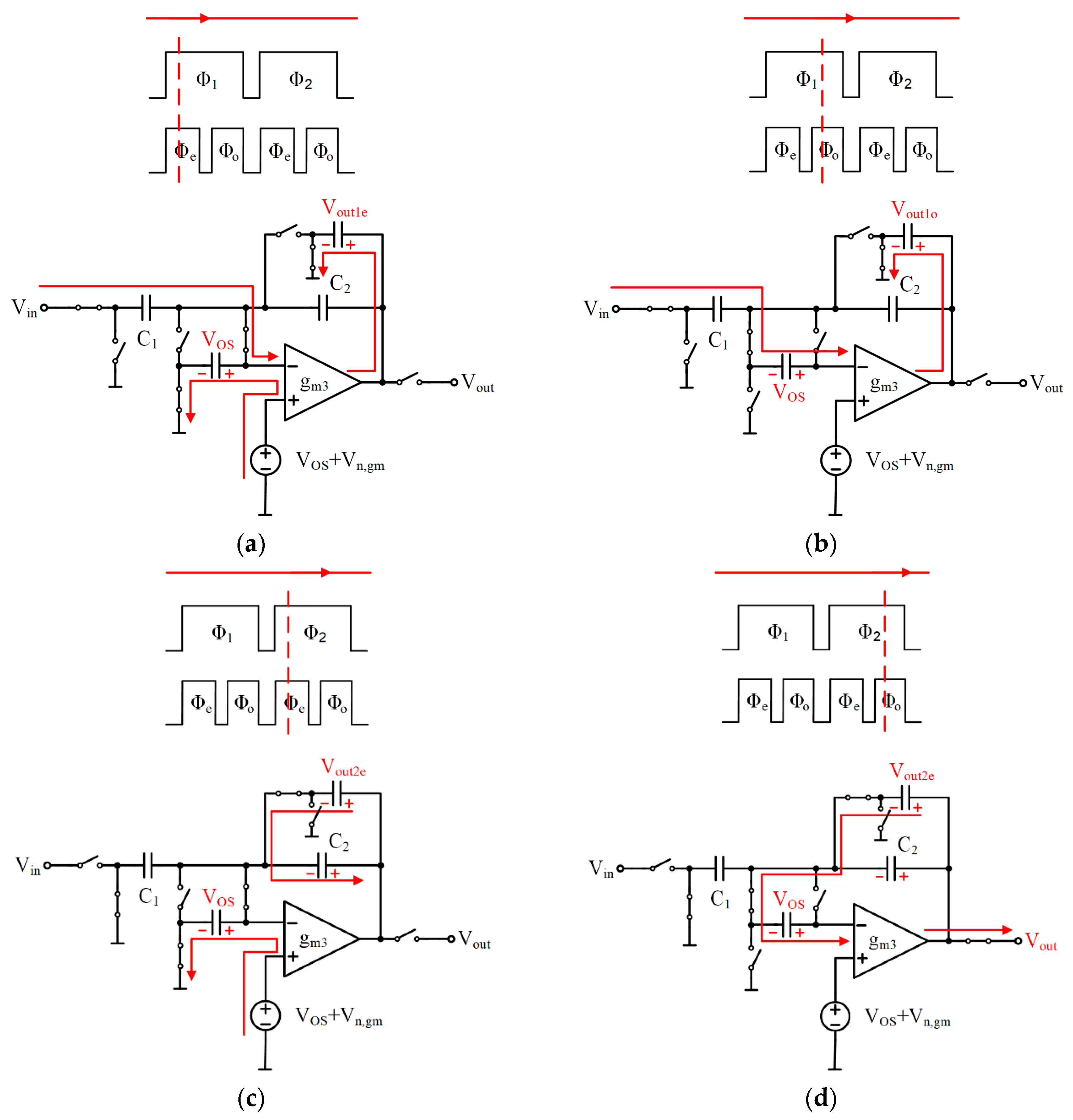
The equivalent circuit of the SC integrator for each phase and the signals transmission direction are demonstrated in Figure 2. As shown in Figure 2a, during phase 1e, SC integrator behaves as a traditional capacitively-coupled amplifier and the op amp output is given as
where T is the clock period. Note that the output switch is turned off and the op amp output is directly connected to capacitors C3 and C2. As the left plate of capacitor C3 is connected to be grounded, the output of the op amp is sampled by C3 rather than directly output in this phase. At the same time, the input offset voltage and low-frequency noise of the op amp are recorded by the capacitor CS through the same principle.
As shown in Figure 2b, during phase 1o, the difference from phase 1e is that the input signal passes through the capacitor CS before being connected to the input of the op amp. Thus, the interference voltages of the op amp sampled by the capacitor CS in the previous phase is subtracted. The output signal is still recorded by capacitor C3.
As shown in Figure 2c, during phase 2e, the input switch is turned off. The stored charge of C3 is redistributed to C2. The new voltage on the capacitor Vout2e can be given as
Like phase 1e, the offset voltage and low-frequency noise voltage are stored by the capacitor CS again.
As shown in Figure 2d, during phase 2o, the divided voltage Vout2e is connected to the input of the op amp through the capacitor Cs. The offset voltage and low-frequency noise voltage of the op amp is subtracted as well. In this phase, the divided voltage Vout2e is amplified and then output.
As a consequence, the voltage Vout1lo sampled in phase 1o is not directly connected to the output after being integrated but is stored on the capacitor C3. It is redistributed with C2 and then acts as the input signal to be integrated at phase 2o for the second time. After these processes, the signal is output in the last phase 2o.
The time-domain transfer function of the entire system can be obtained as
in which superscript o indicates odd phase (Φo) and superscript e indicates even phase (Φe).
The z-domain transfer function is given by
The integral unit gain band frequency can be derived from Equation (5). It can be given as
where fcVLT is the switching clock frequency used in SC integrator.
Compare Equation (6) with Equation (1), the VLT SC integrator can achieve a much smaller unit-gain bandwidth than traditional integrator with the same value capacitances C1 and C2, as it is proportional to the square of C2/C1. Consequently, it can be used in dc servo loop to achieve a much lower high-pass corner frequency to improve the area-efficient. In addition, as shown in Equation (6), the unit-gain bandwidth can be adjusted by changing the external input switching frequency fcVLT.
As shown in Figure 1b, the dc offset voltage VOS and RTI noise of op amp Vn,gm both have a contribution to output voltage and their z-domain transfer function is
As shown in Equation (7), these interferences are also amplified to the output of the integrator. It is inevitable to attenuate these interferences if we want the signal to be undisturbed.
Compared with traditional VLT integrator, there are two extra phases (phase e, phase o) under phase 1 and phase 2 in the switching clock scheme for noise and offset compensation. Capacitor CS is connected to the ground to sample the dc offset voltage and low-frequency noise during phase e and hold this voltage during phase o. Thus, these main interference voltages can be subtracted from the input signal before entering the op amp. As illustrated in the operation of the SC circuit at each phase, in phase 1o and phase 2o, the offset and low-frequency noise are both compensated. Moreover, the effect of finite op amp gain can also be reduced to a negligible proportion by using this structure.
An alignment problem will exist in switching the clock scheme. Four phases are generated by an external clock signal. Buffers have been used to make sure they have the same delay time. The asymmetry, rising time, and falling time of phase 1 and 2 has an impact on noise and gain performance of the SC integrator. To make sure input signal passes through capacitor CS at the end of phase 1 and 2, phase o needs to be relatively delayed.
2.2. System Structure of Chopper Amplifier
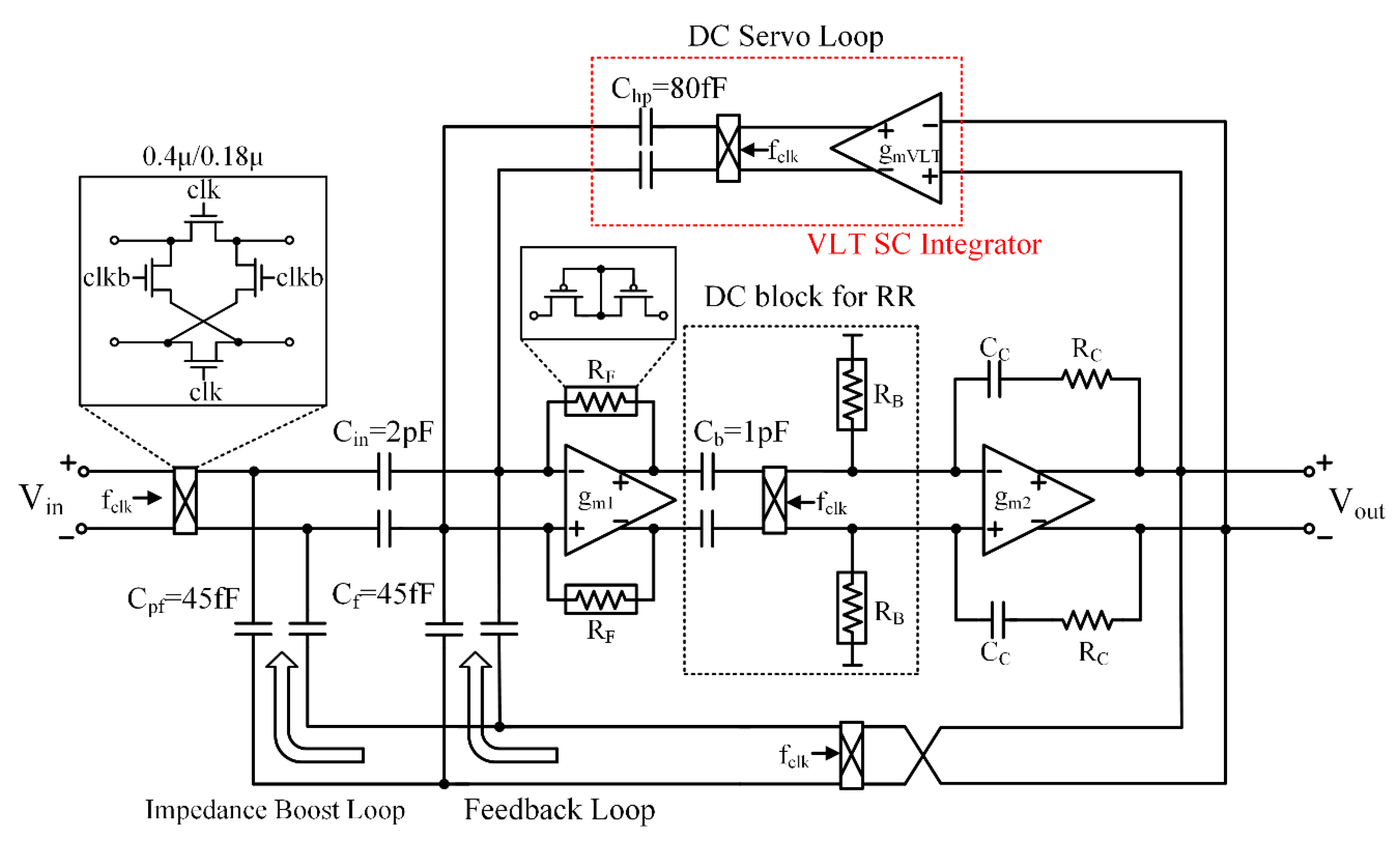
Figure 3 shows the complete structure of the FEA. It consists of four main blocks. The first block is the capacitively-coupled two-stage transconductor (gm1, gm2). The gain of the whole chopper-stabilized amplifier equals to the ratio of input capacitance and feedback capacitance Cin/Cf. As mentioned before, there is a dc servo loop composed of the VLT SC integrator which is introduced in the previous section. The third part is the dc-blocking impedance for ripple rejection which is the same as that in [16]. The output ripples can be reduced by filter the dc offset and the low-frequency noise of gm1. The fourth block is the positive feedback loop, which provides positive feedback current to input to boost the input impedance.
The dc servo loop comprises a chopper, two capacitors Chp and the proposed VLT integrator. The bandwidth of the high-pass filter created by servo loop is given by
By using Equations (6) and (8), the high-pass corner frequency can be calculated as
Due to the high precision of ratio of capacitances, the high-pass corner frequency fhp has a precise range from 0.5 Hz to 5 Hz while occupying a small chip area. In the proposed design, when switching at 10 kHz, C2/C1 equals to 16 pF/250 fF, and Chp/Cf is set to 80 fF/45 fF. The high-pass corner frequency can be calculated as 0.5 Hz.
As shown in the left box in Figure 3, the size of NMOS switches used in chopper is 0.4 μm/0.18 μm, which is minimized to reduce the charge injection. There is a compromise in the choice of chopping frequency, where the lowest possible chopping frequency is suggested to reduce glitch noise [10]. Furthermore, the influence of the low-frequency noise of the transconductance gm1 needs to be considered when choosing the chopping frequency. If it is too low, the neural signal will suffer from higher-level gm1 noise interference. In this work, the chopping frequency is selected as 20 kHz. Pseudo resistors (PRs) are used in dc block and dc-feedback loop to establish bias voltages (dc path) which can achieve a very large equivalent resistance in a small chip area.
The noise of the FEA is determined by the two stage transconductances, gm1, gm2, and the integrator in the dc servo loop. When considering the equivalent RTI noise of the FEA, the noise contribution of the output stage transconductance gm2 can be greatly suppressed by the gain of the first stage op amp. The remaining two noise sources made the main contribution. The RTI noise of the first stage transconductance gm1 can be equivalent to the input of the FEA. The RTI noise of the integrator is directly connected to output. Denoting the RTI noise of the integrator as and the RTI noise of first stage transconductance gm1 as . Their contribution to the RTI noise of FEA can be given as follows [10]:
where fhp is the high-pass corner.
Chopper-stabilized technical help reduce the noise contribution of gm1 by moving the neural signal to the middle-frequency noise band of the first stage transconductance gm1. is greatly reduced without the interference of the flicker noise. Furthermore, the noise contribution of VLT integrator mainly exist at low-frequency, it can also be minimized by using the proposed offset and low-frequency noise compensation structure which has been analyzed in the previous section. can be greatly reduced by storing the offset and low-frequency noise on the capacitors and subtracting it during the input phase. Therefore, the two main noise contribution of the amplifier shown in Equation (9) are reduced by using these two circuit techniques in combination. By applying the new integrator structure to the chopper amplifier, we have obtained a novel FEA structure with excellent RTI noise performance.
2.3. Design of a Current Reuse Amplifier and a High-Slew-Rate Amplifier
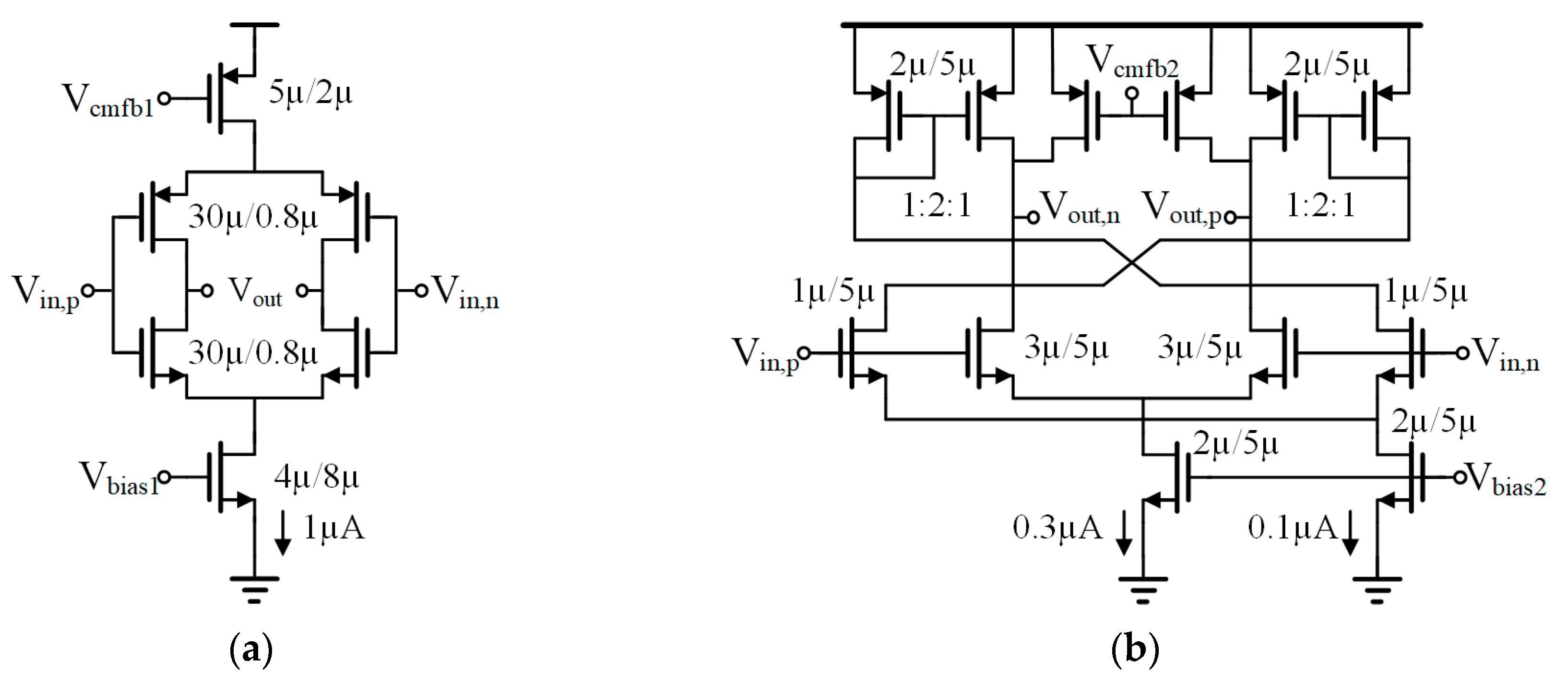
The circuits of the two op amps are shown in Figure 4. The first stage uses the current reuse structure which has complementary input pairs through the same current resource. It improves gm/Id by a factor of √2. In order to obtain the minimal noise and maximum gm/Id, input transistors work in the deep subthreshold region. The size of bias transistors is a tradeoff between the noise and the phase margin. The stability of the common-mode feedback loop is sensitive to the size of the top transistor in Figure 4a. In addition, all transistors should be made as large as possible to minimize 1/f noise [2].
The output stage uses a class-AB amplifier to provide high-slew-rate. Additionally, excellent performance on power supply rejection and input common-mode rejection is also achieved by this structure. Resistors RC and capacitors CC are connected between the output and input of the second stage for miller compensation.
3. Results
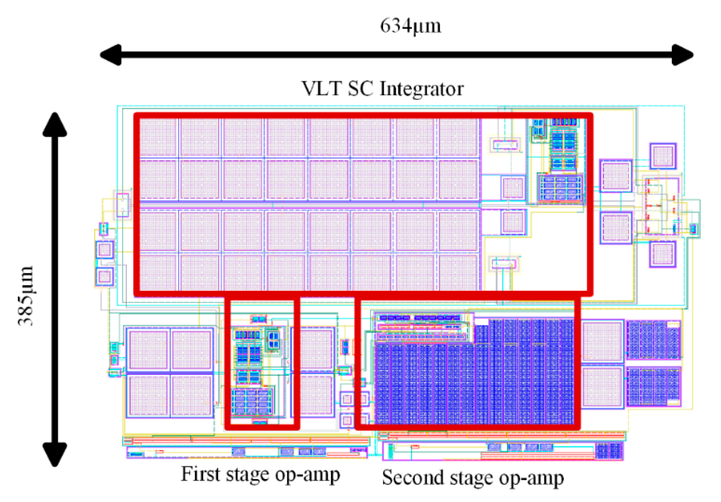
The proposed chopper-stabilized instrument amplifier is designed in a 0.18-µm 1P6M 1.8-V CMOS process. All simulation results are based on post-layout simulation using the Spectre of Cadence Virtuoso 6.1 EDA software (Cadence, San Jose, CA, USA). The parasitic parameter extraction type is transistor level, R + C + CC with no inductance. The layout structure of a single-channel FEA is shown in Figure 5. The layout area of this amplifier is 0.244 mm2. For low-noise and low-power neural signal detection applications, the performance of the entire chopper amplifier and its key modules are simulated.
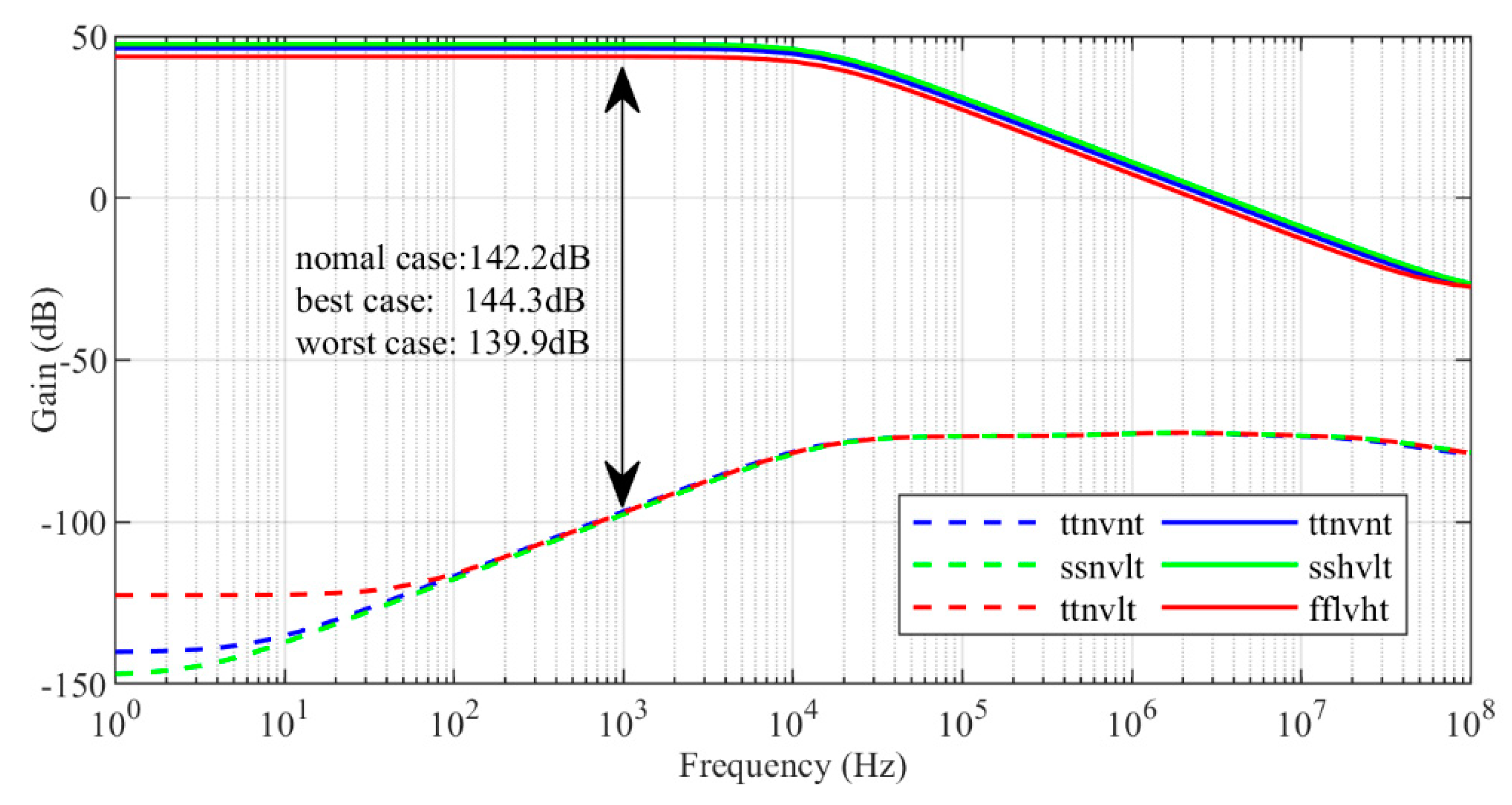
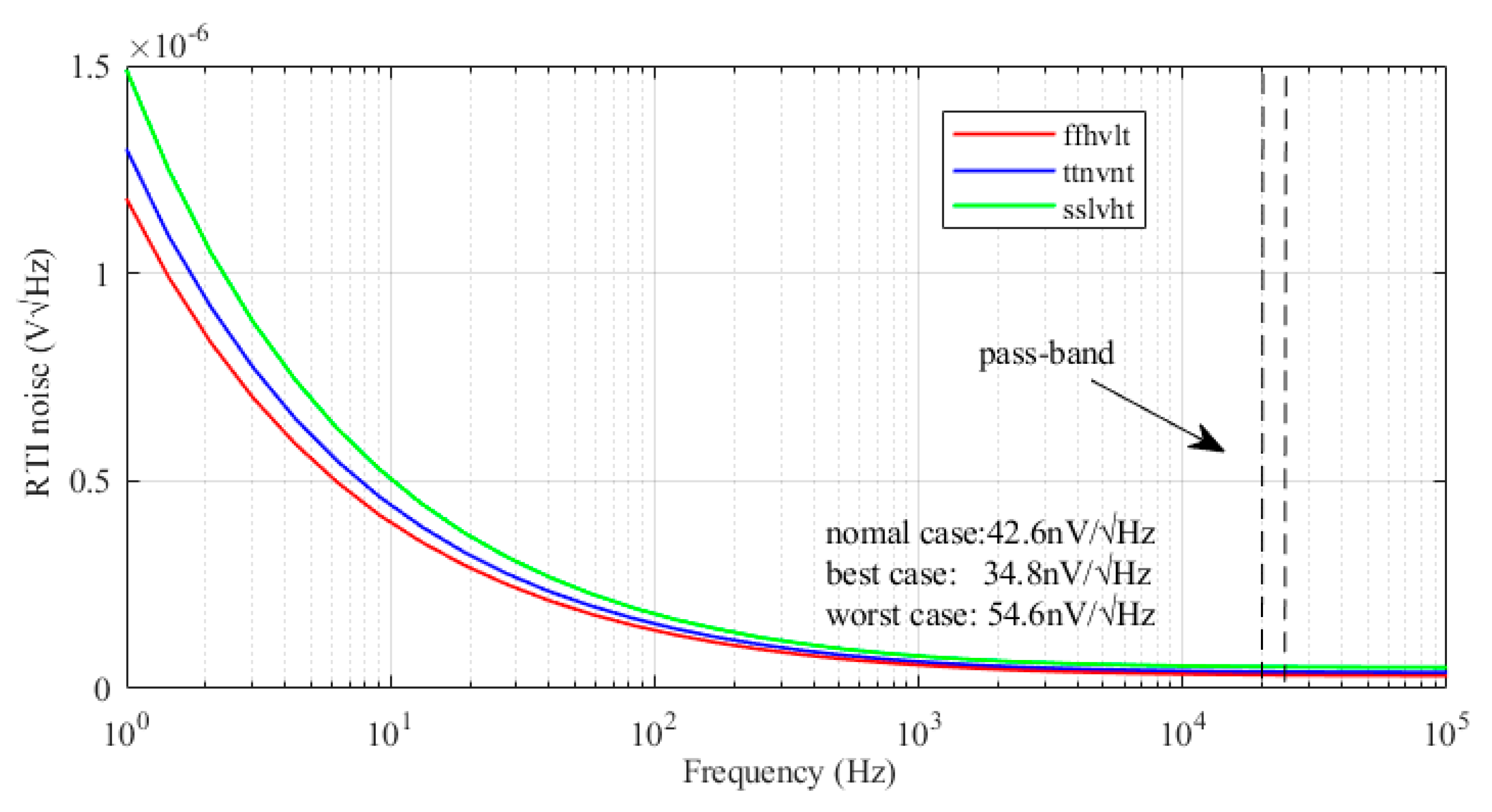
The first stage op amp using the current reuse structure has a decisive influence on the performance of the proposed FEA. Figure 6 shows its differential mode and common mode signal transfer function. In order to verify the stability of the chip in different PVT environments, three processes: tt, ff, ss; three supply voltages: normal voltage (nv) 1.8 V, high voltage (hv) 1.98 V, low voltage (lv) 1.62 V; and three temperatures: normal temperature (nt) 60°, high temperature (ht) 125°, low temperature (lt) −40° are considered. The CMRR is given by subtracting the common mode gain from the differential mode gain. It has a range of 144.3 dB to 139.9 dB at 1 kHz. Figure 7 shows the noise performance of the current reuse structured amplifier. The simulated referred-to-input noise spectrum density has a range of 34.8 nV/√Hz to 54.6 nV/√Hz in the neural signal pass-band after being upmodulated.
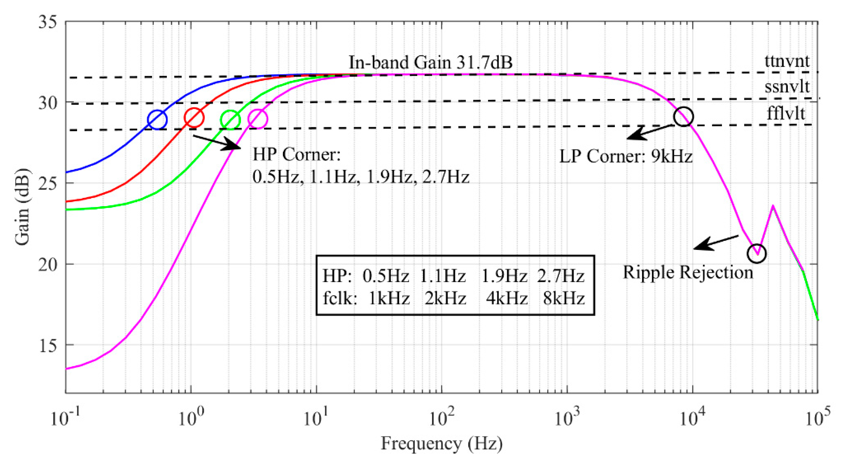
The signal transfer function of the FEA is shown in Figure 8. By changing the frequency of the external input clock signal of SC integrator from 1 kHz to 8 kHz, the high-pass corner of the neural amplifier can be changed from 0.5 Hz to 4.0 Hz, respectively. According to Equations (4) and (5), the gain of the VLT integrator is also influenced by the clock frequency. When the high-pass corner decreases, the gain of integrator also decreases. As the ratio of input capacitor and feedback capacitor Cin/Cf = 2 pF/45 fF, in-band gain equals to 31.7 dB. Under the worst case (ff, 1.62 V, 0°), its in-band gain equals to 28 dB. The low-pass corner is 9 kHz which is sufficient for neural signal recording application. There is a notch at 20 kHz because of ripple rejection block.
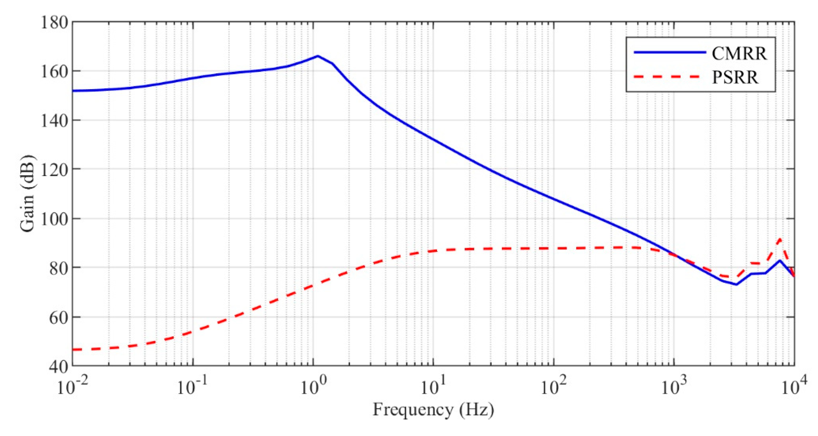
The CMRR and PSRR of chopper amplifier are shown in Figure 9. PSRR has a flat curve in the pass-band of 87.7 dB; meanwhile, CMRR has a curve that is inversely proportional to frequency in the pass-band, which takes a value of 113.7 dB at 50 Hz. These two curves show that the FEA can effectively suppress common mode input interference signals and power fluctuation interference signals during detection.
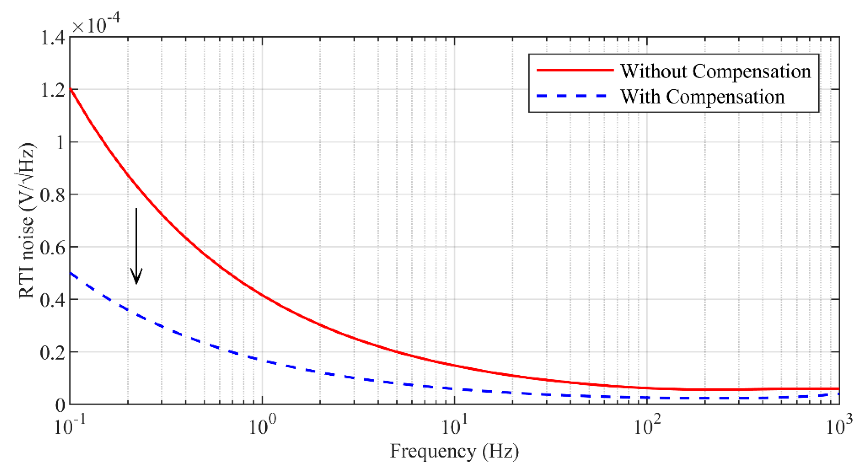
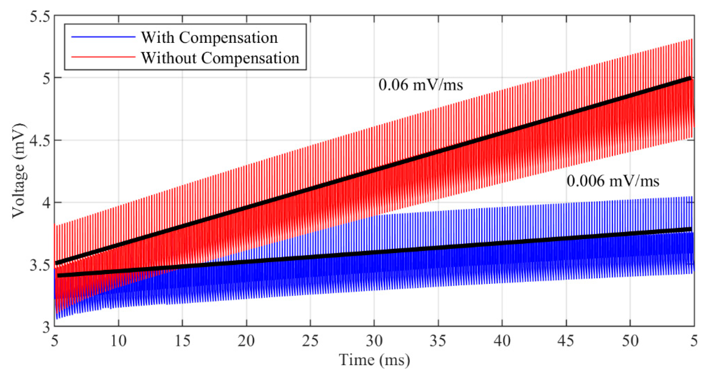
The effectiveness of compensation technique on low-frequency noise compensation and offset compensation used in the integrator is shown in Figure 10 and Figure 11. The result shows that RTI noise of the VLT SC integrator can be attenuated by 58% at 0.1 Hz compared without compensation integrator which is obtained by using periodic steady-state noise simulation. In the absence of the input signal, the rate of the output shift caused by the integral of offset voltage is also attenuated by 10 times by the compensation technique. This result is obtained by using transient response simulation.
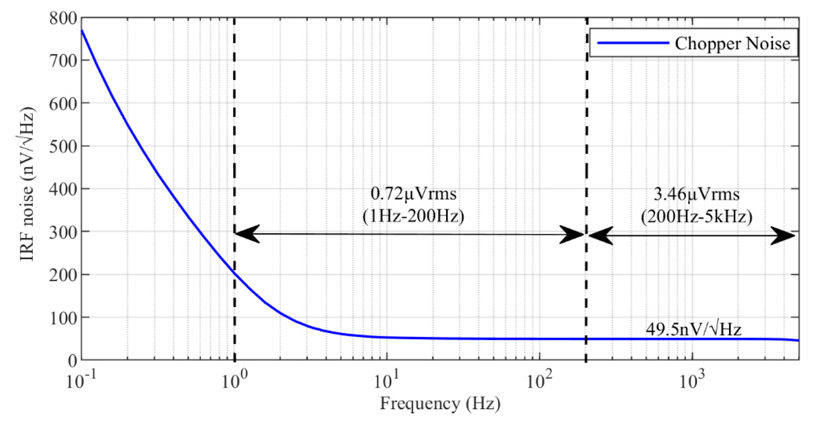
The RTI noise of the whole proposed amplifier is represented in Figure 12, and the integrated noise is 0.72 µVrms in the AP band (1 Hz~200 Hz) and 3.46 µVrms in the LFP band (200 Hz~5 kHz). Noise effect factor (NEF) can be given as
where bandwidth equals to 9 kHz, temperature equals to 300 K, and thermal voltage VT equals to 26 mV. NEF can be calculated as 2.08 in the AP band and 0.43 in the LFP band.
The sub-hertz high-pass corner is realized with a small chip area through the very-large-time-constant switched-capacitor integrator structure which guarantees the low-frequency neural signal acquisition, and the electrode dc offset will be attenuated. The simulation results of the CMRR, PSRR, and the transfer function under different process corners, voltages, and temperatures prove the stability of the proposed FEA. The RTI noise spectrum of the chopper amplifier and the decrease in the offset voltage of the integrator is consistent with the theoretical derivation, which proves the effectiveness of the proposed offset and low-frequency noise compensation structure.
Table 1 summarizes the detail parameter values of this work and comparisons with current state-of-the-art research. This work has an improved performance on bandwidth, input-referred noise and NEF. It is also competitive in terms of power consumption and chip area.
4. Conclusions
This paper presents a chopper-stabilized analog FEA for neural detection. A new dc servo loop is proposed to decrease its low-frequency noise and dc offset contribution. The proposed FEA has a precise high-pass corner frequency to solve the interference of the electrode dc offset. The extra phases are proposed to store and compensate for the noise and dc offset in the VLT integrator. A complementary input stage and a high-slew-rate output stage is employed to drive a large capacitor load while working at low power consumption and having sufficient bandwidth. The post-simulated results show RTI noise of the improved integrator decrease 58% in 0.1 Hz (regarding to traditional design), and the chopper amplifier RTI noise has a floor of 49.5 nV/√Hz. This structure achieves low input-referred noise and NEF performance in regards to biomedical applications. This technique also achieves high CMRR (>85 dB), high PSRR (>87 dB), and small area (0.244 mm2).
Author Contributions
Y.L., Z.Z. and Y.Z. designed the circuit as well as the layout and simulation. W.L. and Z.W. supervised the project. All authors have read and agreed to the published version of the manuscript.
Funding
This work was supported by the Provincial Natural Science Foundation of Jiangsu Province (BK20180363), National Natural Science Foundation of China with Grant No. 61874024 and 62004036, Fundamental Research Funds for the Central Universities, and the Opening Project of State Key Laboratory of Bioelectronics, Southeast University, Nanjing 210096, China.
Conflicts of Interest
The authors declare no conflict of interest.
References
- Webster, J.G. Medical Instrumentation: Application and Design; Wiley: New York, NY, USA, 1998. [Google Scholar]
- Ng, K.A.; Greenwald, E.; Xu, Y.P.; Thakor, N.V. Implantable neurotechnologies: A review of integrated circuit neural amplifiers. Med. Biol. Eng. 2016, 54, 45–62. [Google Scholar] [CrossRef] [PubMed] [Green Version]
- Harrison, R.R.; Charles, C. A low-power low-noise CMOS amplifier for neural recording applications. IEEE J. Solid State Circuits 2003, 38, 958–965. [Google Scholar] [CrossRef]
- Denison, T.; Consoer, K.; Santa, W.; Avestruz, A.-T.; Cooley, J.; Kelly, A. A 2 μW 100 nV/√Hz chopper-stabilized instrumentation amplifier for chronic measurement of neural field potentials. IEEE J. Solid State Circuits 2007, 42, 2934–2945. [Google Scholar] [CrossRef]
- Chandrakumar, H.; Marković, D. A high dynamic-range neural recording chopper amplifier for simultaneous neural recording and stimulation. IEEE J. Solid State Circuits 2017, 52, 645–656. [Google Scholar] [CrossRef]
- Fan, Q.; Sebastiano, F.; Huijsing, J.H.; Makinwa, K.A.A. A 1.8 μW 60 nV/√Hz capacitively-coupled chopper instrumentation amplifier in 65 nm CMOS for wireless sensor nodes. IEEE J. Solid State Circuits 2011, 46, 1534–1543. [Google Scholar] [CrossRef]
- Wu, R.; Makinwa, K.A.A.; Huijsing, J.H. A chopper current-feedback instrumentation amplifier with a 1 mHz 1/f noise corner and an AC-coupled ripple-reduction loop. IEEE J. Solid State Circuits 2009, 44, 3232–3243. [Google Scholar] [CrossRef] [Green Version]
- Xu, J.; Lin, Q.; Ding, M.; Li, Y.; van Hoof, C.; Serdijn, W.; van Helleputte, N. A 0.6 V 3.8 μW ECG/bio-impedance monitoring IC for disposable health patch in 40 nm CMOS. In Proceedings of the 2018 IEEE Custom Integrated Circuits Conference (CICC), San Diego, CA, USA, 8–11 April 2018; pp. 1–4. [Google Scholar]
- Li, Q.; Wang, X.; Liu, Y. A 60nV/√Hz <0.01%-THD ±200 mV-DC-Rejection Bio-Sensing Chopper Amplifier with Noise-Nonlinearity-Cancelling Loop. IEEE Trans. Circuits Syst. II Express Briefs 2020, 67, 215–219. [Google Scholar] [CrossRef]
- Luo, D.; Zhang, M.; Wang, Z. A Low-Noise Chopper Amplifier Designed for Multi-Channel Neural Signal Acquisition. IEEE J. Solid State Circuits 2019, 54, 2255–2265. [Google Scholar] [CrossRef]
- Enz, C.C.; Temes, G.C. Circuit techniques for reducing the effects of op-amp imperfections: Autozeroing, correlated double sampling, and chopper stabilization. Proc. IEEE 1996, 84, 1584–1614. [Google Scholar] [CrossRef] [Green Version]
- Radev, N.A.; Ivanov, K.P. Area-efficient gain- and offset-compensated very-large-time-constant SC integrator. Electron. Lett. 2000, 36, 394–396. [Google Scholar] [CrossRef]
- Ivanisevic, N.; Rodriguez, S.; Rusu, A. Area-Efficient Switched-Capacitor Integrator with Flicker Noise Cancellation. In Proceedings of the 2018 IEEE International Symposium on Circuits and Systems (ISCAS), Florence, Italy, 27–30 May 2018; pp. 1–4. [Google Scholar]
- Xu, J.; Fan, Q.; Huijsing, J.H.; van Hoof, C.; Yazicioglu, R.F.; Makinwa, K.A.A. Measurement and Analysis of Current Noise in Chopper Amplifiers. IEEE J. Solid State Circuits 2013, 48, 1575–1584. [Google Scholar]
- Wang, X.; Shi, Z.; Xu, B. Noise optimization of switched capacitor integrator. In Proceedings of the 2015 IEEE International Conference on Electron Devices and Solid-State Circuits (EDSSC), Singapore, 1–4 June 2015; pp. 519–522. [Google Scholar]
- Chandrakumar, H.; Marković, D. A simple area-efficient ripple-rejection technique for chopped biosignal amplifiers. IEEE Trans. Circuits Syst. II Express Briefs 2015, 62, 189–193. [Google Scholar] [CrossRef]
- Khatavkar, P.; Aniruddhan, S. 432 nW per Channel 130 nV/√Hz ECG Acquisition Front End with. Multifrequency Chopping. IEEE Trans. Large Scale Integr. Vlsi Syst. 2019, 27, 2021–2032. [Google Scholar] [CrossRef]
- Liang, Z.; Li, B.; Wu, Z. A Fully Integrated Chopper IA for Implantable Multichannel EEG Recording Without Impedance Boosting Circuits. In Proceedings of the 2018 IEEE Asia Pacific Conference on Circuits and Systems (APCCAS), Chengdu, China, 26–30 October 2018; pp. 143–146. [Google Scholar]
- Xu, W.; Wang, T.; Wei, X.; Yue, H.; Wei, B.; Duan, J.; Li, H. Low Noise, High Input Impedance Digital-Analog Hybrid Offset Suppression Amplifier for Wearable Dry Electrode ECG Monitoring. Electronics 2020, 9, 165. [Google Scholar]
Figure 1.
(a) Schematic of traditional switched-capacitor integrator and its switching clock scheme. (b) Schematic of the proposed very-large-time-constant switched-capacitor integrator with offset and low-frequency noise compensation and its switching clock scheme.
Figure 1.
(a) Schematic of traditional switched-capacitor integrator and its switching clock scheme. (b) Schematic of the proposed very-large-time-constant switched-capacitor integrator with offset and low-frequency noise compensation and its switching clock scheme.

Figure 2.
Equivalent circuit diagram of different phases: (a) 1e, (b) 1o, (c) 2e, (d) 2o. The signals transmission direction is shown by the red line.
Figure 2.
Equivalent circuit diagram of different phases: (a) 1e, (b) 1o, (c) 2e, (d) 2o. The signals transmission direction is shown by the red line.

Figure 3.
Complete structure of the proposed capacitively-coupled chopper instrument amplifier with the very-large-time switched-capacitor integrator.
Figure 3.
Complete structure of the proposed capacitively-coupled chopper instrument amplifier with the very-large-time switched-capacitor integrator.

Figure 4.
(a) The structure of the first stage transconductance gm1, (b) the structure of the output stage transconductance gm2.
Figure 4.
(a) The structure of the first stage transconductance gm1, (b) the structure of the output stage transconductance gm2.

Figure 5.
Layout of the proposed chopper-stabilized instrument amplifier.

Figure 6.
Differential mode and common mode signal transfer function of first stage transconductance gm1 under process, voltage, and temperature variation.
Figure 6.
Differential mode and common mode signal transfer function of first stage transconductance gm1 under process, voltage, and temperature variation.

Figure 7.
Referred-to-input noise spectrum density of first stage transconductance gm1 under process, voltage, and temperature variation.
Figure 7.
Referred-to-input noise spectrum density of first stage transconductance gm1 under process, voltage, and temperature variation.

Figure 8.
Signal transfer function of chopper amplifier at different fclk.

Figure 9.
CMRR and PSRR of chopper amplifier.

Figure 10.
Referred-to-input noise spectrum density of very-large-time-constant (VLT) switched-capacitor (SC) integrator.
Figure 10.
Referred-to-input noise spectrum density of very-large-time-constant (VLT) switched-capacitor (SC) integrator.

Figure 11.
The transient waveform of the VLT SC integrator without input signal.

Figure 12.
Referred-to-input noise spectrum density of proposed chopper amplifier.


Table 1.
Comparison with current state-of-the-art research.
| Parameter | [5] | [10] | [17] | [18] | [19] | This Work |
|---|---|---|---|---|---|---|
| Technology | 40 nm | 65 nm | 130 nm | 180 nm | 180 nm | 180 nm |
| Gain (dB) | 26 | 40 | 40 | 40–54 | 46 | 31.7 |
| Bandwidth (Hz) | 5 k | 500 | 100 | 5 k | 500 | 9 k |
| Input-referred noise (µVrms) | LFP: 2 1 AP: 7 2 | LFP: 6.7 1 | AP: 2.62 2 | 1–100 Hz: 1.06 1–5 kHz: 5.23 | AP: 1.9 2 | LFP: 0.72 1 AP: 3.46 2 |
| NEF | LFP: 7 1 AP: 4.9 2 | LFP: 14 1 | AP: 6.05 2 | 1–100 Hz: 3.31 1–5 kHz: 2.31 | AP: 11.4 2 | LFP: 0.43 1 AP: 2.08 2 |
| CMRR (dB) | >78 | >110 | 98 | 97 (1 kHz) | 96 (50 Hz) | >85 |
| PSRR (dB) | - | >100 | - | - | - | >87 |
| Power/Ch (µW) | 2 | 1.8 | 0.432 | 0.792 | 19.8 | 3.96 |
| Area/ch (mm2) | 0.071 | 0.2 | 0.68 | 0.15 | 0.36 | 0.244 |
1 LFP: local filed potential (1 Hz~200 Hz); 2 AP: action potential (200 Hz~5 kHz).
Publisher’s Note: MDPI stays neutral with regard to jurisdictional claims in published maps and institutional affiliations. |
© 2020 by the authors. Licensee MDPI, Basel, Switzerland. This article is an open access article distributed under the terms and conditions of the Creative Commons Attribution (CC BY) license (http://creativecommons.org/licenses/by/4.0/).
Share and Cite
MDPI and ACS Style
Liu, Y.; Zhou, Z.; Zhou, Y.; Li, W.; Wang, Z. A Low-Noise Chopper Amplifier with Offset and Low-Frequency Noise Compensation DC Servo Loop. Electronics 2020, 9, 1797. https://doi.org/10.3390/electronics9111797
AMA Style
Liu Y, Zhou Z, Zhou Y, Li W, Wang Z. A Low-Noise Chopper Amplifier with Offset and Low-Frequency Noise Compensation DC Servo Loop. Electronics. 2020; 9(11):1797. https://doi.org/10.3390/electronics9111797
Chicago/Turabian StyleLiu, Yuekai, Zhijun Zhou, Yixin Zhou, Wenyuan Li, and Zhigong Wang. 2020. "A Low-Noise Chopper Amplifier with Offset and Low-Frequency Noise Compensation DC Servo Loop" Electronics 9, no. 11: 1797. https://doi.org/10.3390/electronics9111797
Note that from the first issue of 2016, this journal uses article numbers instead of page numbers. See further details here.