
Deep Neural Networks-Based Direct-Current Operation Prediction and Circuit Migration Design


1
School of Electronic Science and Engineering, Xiamen University, Xiamen 361005, China
2
School of Intergated Circuits, Tsinghua University, Beijing 100084, China
*
Authors to whom correspondence should be addressed.
Electronics 2023, 12(13), 2780; https://doi.org/10.3390/electronics12132780
Submission received: 29 May 2023
/
Revised: 18 June 2023
/
Accepted: 20 June 2023
/
Published: 23 June 2023
(This article belongs to the Section Circuit and Signal Processing)
Abstract
:Recently, design methods based on parameters have attracted attention in analog integrated circuit design and have been automated with computer assistance. However, the look-up tables (LUTs) in the method have the problem of high hardware resource overhead. To address this issue, this paper proposes a multi-output deep neural network (DNN) structure for modeling the direct-current parameters of transistors and replacing LUTs for circuit design. The proposed DNN models’ performance is verified using mainstream design technologies such as TSMC 40 nm (T40), TSMC 65 nm (T65), TSMC 180 nm (T180), and SMIC 180 nm (S180). Compared with LUTs, the proposed DNN models are able to reduce at least 99.9% storage space occupation and 95.62% prediction time overhead with a mean absolute percentage error of less than 0.2%. In addition, we propose an automated circuit migration design method using DNN models in different technologies, combined with parameters. The method generates circuit design databases in different technologies and obtains device design results according to performance requirements. The experimental results show that using DNN models can reduce the time overhead by more than 40% compared to using LUTs. The simulation results of circuit transplantation design show that the circuit performance of T40, T65, S180, and T180 meets the requirements, which verifies the proposed DNN-based automated circuit design method.
1. Introduction
In the current era of mixed-signal system-on-chips, digital integrated circuit (IC) design has the benefit of relying on mature automated synthesis tools for automated design. In contrast, analog IC design is a time-consuming task that heavily relies on manual analysis by expert designers due to the lack of mature automated synthesis tools [1]. This manual design process is a bottleneck in IC design, prompting the need for automated analog IC design technologies, which have garnered widespread attention.
The mainstream approaches to automation can be broadly categorized into two types: optimization-based and knowledge-based methods [2]. The optimization-based approach utilizes optimization algorithms such as evolutionary algorithms [3] to generate new device size results. However, due to the inherent complexity of both algorithms and circuits, this approach may result in significant time consumption or even physically infeasible solutions [4].
The knowledge-based approach, on the other hand, relies on expert knowledge to develop automated design programs capable of generating valuable solutions. Currently, the mature approach is based on the method [5] with pre-computed lookup tables (LUTs) [6], which achieves high design accuracy and has been successfully applied in the design of various circuits such as operational amplifiers, bandgap reference circuits, low-noise amplifiers, and others [7,8,9,10,11].
The LUTs used in the method are generated by simulating the device parameters using a simulation program with integrated circuit emphasis (SPICE) models with fixed step sizes in channel length (L), , , and . For parameter values that are not present in the LUTs, interpolation can be utilized to predict the values. However, high-precision LUTs require more finely scanned parameter step sizes, leading to increased storage space usage [12]. Taking into account the number of model parameters and device types, the large storage space requirements and the need to load them into memory for access entail significant hardware resource costs, rendering this design method impractical.
With the continuous advancements in machine learning (ML), researchers have started exploring the possibility of constructing device parameter models using ML models. Habal et al. [13] developed a simple quadratic polynomial as a feature engineering input and proposed a neural network with a single hidden layer for predicting . In the work of Habal et al., the prediction errors of the ML model were approximately controlled within 3%. However, predicting a single parameter of a transistor in a specific technology appears to be insufficient.
Yang et al. [14] conducted a thorough analysis of the impact of different activation functions in a multi-layer perceptron model for predicting the parameters of various transistors. They proposed a neural network architecture with three hidden layers and found that the inverse square root unit (ISRU) activation function provided the best training results. The mean absolute percentage error (MAPE) for the negative channel-metal-oxide-semiconductor (NMOS) was reduced to 1.38%, but the errors for the positive channel metal-oxide-semiconductor (PMOS) ranged between 6.47% and 10.69%. Although these studies demonstrate the potential of multi-layer perceptron models instead of LUTs, the challenge lies in determining the optimal hyperparameters of the neural network.
Ho et al. [15] proposed an algorithm that utilizes genetic algorithms and multi-layer perceptrons to predict current () using an evolved neural network. Their work demonstrated that the prediction accuracy of the evolved neural network was superior to that of a conventional multi-layer perceptron. This research provides some inspiration for our current work as it highlights the potential of using genetic algorithms to optimize neural networks and improve prediction accuracy.
Wang et al. [16] introduced a direct-current (DC) simulation-based neural network model called the DC model. This model utilizes graphics card-accelerated neural networks to capture the non-linear relationship between specific DC parameters and performance metrics. By substituting certain simulation tasks, it significantly reduces time consumption while maintaining a high level of accuracy. Qi et al. [17] proposed a knowledge-based neural network approach that segregates geometric variables from other input variables. The geometric variables are modeled using physics-based analytical equations, while the remaining variables are represented by an artificial neural network. This methodology was verified using the BSIM6 (BSIM, a simulation model developed by the UC Berkeley) model and demonstrated good agreement between the model predictions and experimental results. Similarly, Wang et al. [18] conducted similar work by modifying the BSIM model for low-temperature conditions in a 180 nm technology. They introduced an optimization model based on the backpropagation neural network prediction to compensate for the low-temperature effect. A common characteristic of the aforementioned approaches is the utilization of neural networks to substitute certain aspects of physical modeling, thereby accelerating scientific computations.
Fu et al. [19] presented a model based on the backpropagation neural network for the prediction of NMOS performance parameters. The modeling process involved employing substrate bias, substrate impurity concentration, oxide thickness, and adjusted implant doping concentration for threshold voltage as independent variables while considering threshold voltage and others as dependent variables. Following the training of the model, none of the final prediction variables exhibited an average percentage error exceeding 1.5%.
Wei et al. [20] developed a precise artificial neural network model that encompasses the complete range of drain currents. By employing the Latin hypercube sampling algorithm, they achieved a substantial reduction in the training data requirement without significantly compromising the quality of the fitting outcomes. This approach effectively mitigated training overhead. The experimental findings demonstrate that the proposed artificial neural network model exhibits excellent fitting capabilities in the 180 nm technology.
Most of the above works focus on the parametric modeling of devices, but less work applies the proposed models to actual circuit design. In addition, the technology nodes involved in device parameter modeling focus on one or two technologies, and the effectiveness of the model on more technology is unknown.
This paper introduces a new deep neural network (DNN) architecture that has multiple DC outputs for modeling complementary metal-oxide-semiconductor (CMOS) device parameters. This DNN model requires only four inputs (, , , and L) and can produce 14 outputs simultaneously, including , , , , , , , , , , , , , and . The suggested DNN architecture comprehensively models the device parameters to prevalent process design kits (PDKs) TSMC 40 nm (T40), TSMC 65 nm (T65), TSMC 180 nm (T180), and SMIC 180 nm (S180), respectively. Compared with the traditional LUTs, the proposed DNN models for each PDK occupy less storage space and have high-accuracy prediction performance. Moreover, this paper leverages the DNN models within each PDK, in conjunction with parameters, to achieve circuit migration design. By employing circuit multiplexing, the efficiency of analog integrated circuit design is enhanced.
The structure of the paper is organized as follows: Section 2 introduces the DNN architecture and outlines the necessary metrics requirements. In Section 3, the dataset acquisition process is described. Section 4 discusses the automated design method based on the parameter and DNN models. Section 5 presents the experimental results. Finally, Section 6 is the conclusions.
2. DNN Model and Performance Requirements
2.1. DNN Model Architecture
The mapping of the LUTs used in the method can be described in (1).
For a given PDK (), device type (), and channel width (W), the desired device parameter results such as and can be obtained by the values of , , , and L of the transistor. Typically, LUTs are only capable of providing a single parameter value at a time, and interpolation techniques are employed to obtain parameter data that lie outside the LUTs but fall within the input range.
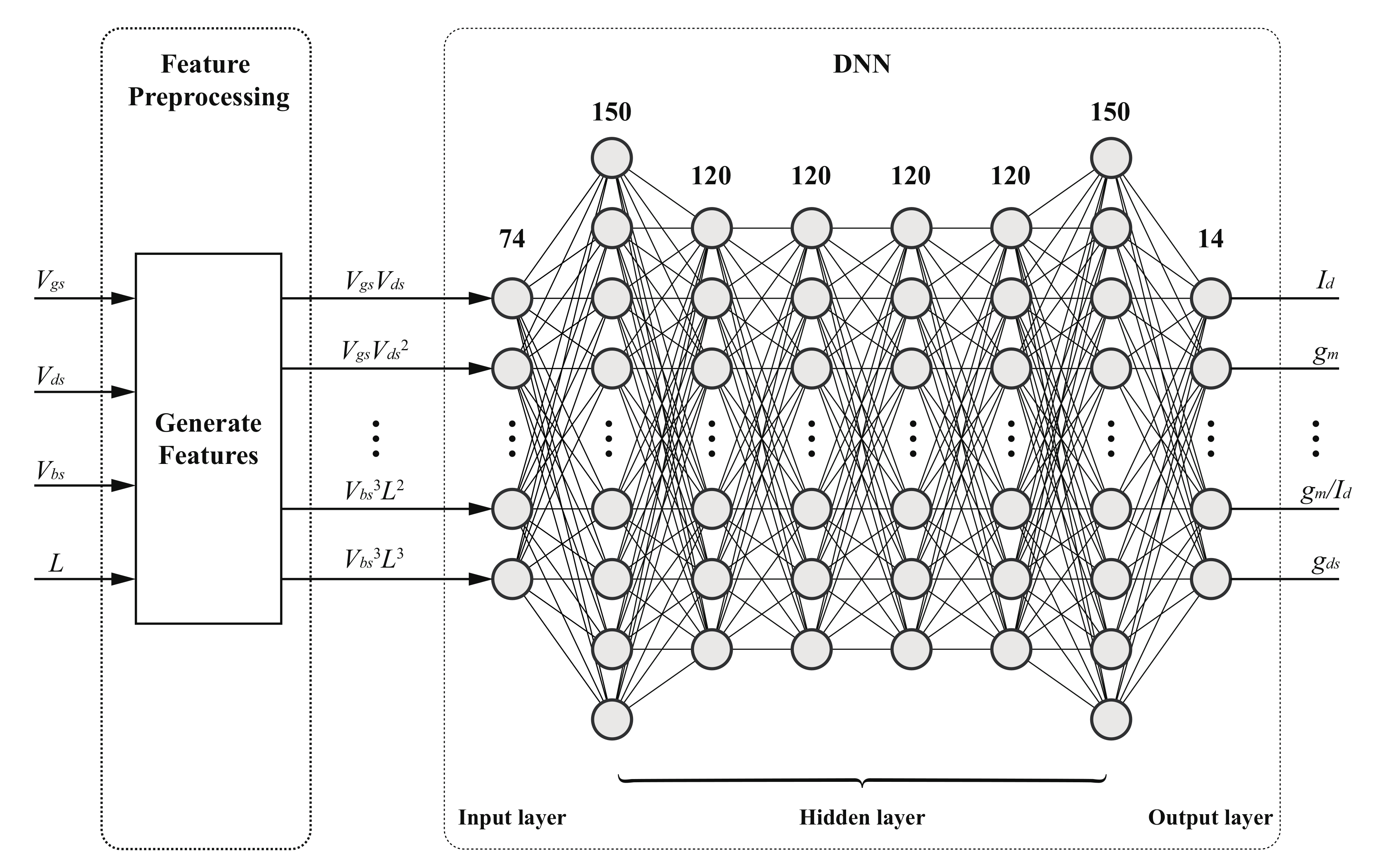
The non-linear relationship between the input and output of the LUTs mentioned above can be modeled using ML approaches. In this paper, a DNN model, as depicted in Figure 1, for training the aforementioned input–output relationship was proposed. The DNN model begins with four input parameters, namely , , , and L. To enhance the representation capability, a feature generation layer is incorporated to generate 74 high-order feature items, which are subsequently utilized as inputs for the DNN. The DNN architecture comprises one input layer, six hidden layers, and one output layer, employing rectified linear unit (ReLU) [21] activation for all hidden layers. The hidden layers consist of 150, 120, 120, 120, 120, and 150 neurons, respectively, and are fully connected. The output layer provides predictions for 14 parameters, encompassing , , , , , , , , , , , , , and . The feature generation algorithm is presented in Algorithm A1, and the training and prediction algorithms of DNN are shown in Algorithm A2 and Algorithm A3, respectively (Appendix A). While the hyperparameter settings for the DNN model are outlined in Table 1.
2.2. Performance Metrics of DNN Model
While the primary motivation behind proposing the DNN model is to address the issue of extensive storage requirements associated with LUTs, it is imperative to consider its capacity to replace LUTs in circuit design while maintaining superior prediction accuracy. Furthermore, the effectiveness of model-based circuit design automation is partially contingent upon the computational speed of the model, as employing a faster prediction model within the same design framework can lead to enhanced design efficiency. In light of the aforementioned analysis, this paper introduces four evaluation metrics, including time, model size, MAPE, and maximum relative error (MRE), to evaluate the performance of the proposed model. Table 2 shows the statement of each metric.
3. Data Sampling
The DNN models are trained using four PDKs: T40, T65, T180, and S180, respectively. The respective ranges and step sizes of the variables used to generate each PDK dataset are presented in Table 3. For T40 and T65, the range of and is set from 0.1 V to 1.2 V, with a step size of 0.02 V for both variables. Similarly, the range of is from 0 V to 1.2 V, with a step size of 0.02 V. On the other hand, for T180 and S180, the range of and is extended from 0.1 V to 1.8 V, and the range of spans from 0 V to 1.8 V, with a consistent step size of 0.02 V for both variables. The channel length (L) values vary from 0.5 µm to 6 µm, with a step size of 0.2 µm, while the channel width (W) remains fixed at 5 µm across all PDKs.
Table 4 provides detailed information regarding the generated datasets, including their sizes and the parameters they encompass. Each dataset comprises 14 device parameters, namely , , , , , , , , , , , , and . The dataset sizes for T40 and T65, which were saved in pickle format, were 1.4 GB space each (including both PMOS and NMOS devices). Similarly, the dataset sizes for T180 and S180 were 4.4 GB space each (including both PMOS and NMOS devices).
Prior to training, the logarithm of the 14 target parameters to be predicted was taken, and the dataset was normalized to eliminate any significant variations among the target parameter data. Subsequently, the dataset was divided into a training set, a validation set, and a test set, following a ratio of 0.81:0.14:0.05, respectively.
4. Sizing Method
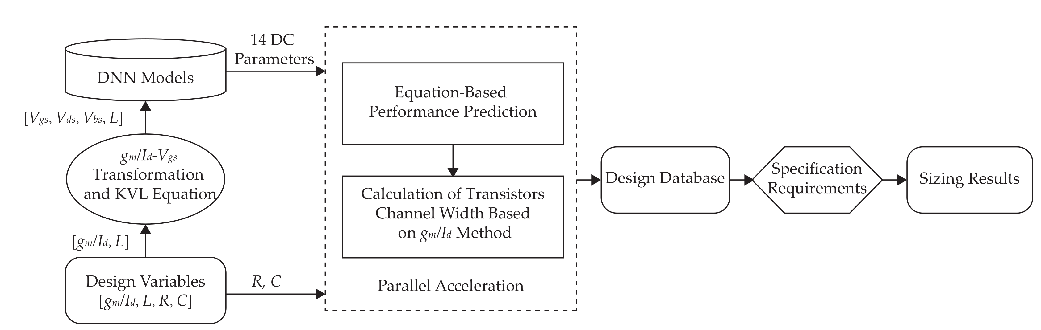
Figure 2 illustrates the design flow used in this work. Specifically, the flow begins by specifying the design variables for the circuit, which include the and L for each transistor, as well as the passive device resistor-capacitor () values. Subsequently, the design points for , , for each transistor are determined using the mapping of and , along with the application of Kirchhoff’s voltage law (KVL) to the circuit. These design points (, , and L) are then input into to obtain 14 DC parameters.
The obtained 14 DC parameters serve two purposes: firstly, they are combined with the circuit performance equations to predict the performance of the circuit. Secondly, they are utilized to solve for the channel width (W) of each transistor based on the method. To expedite this process, parallel computing techniques are employed. Upon traversing all the design points, the values of L, W, R, and C alongside the corresponding circuit performance are stored in the . Finally, the sizing results are outputted according to the performance specifications requirements.
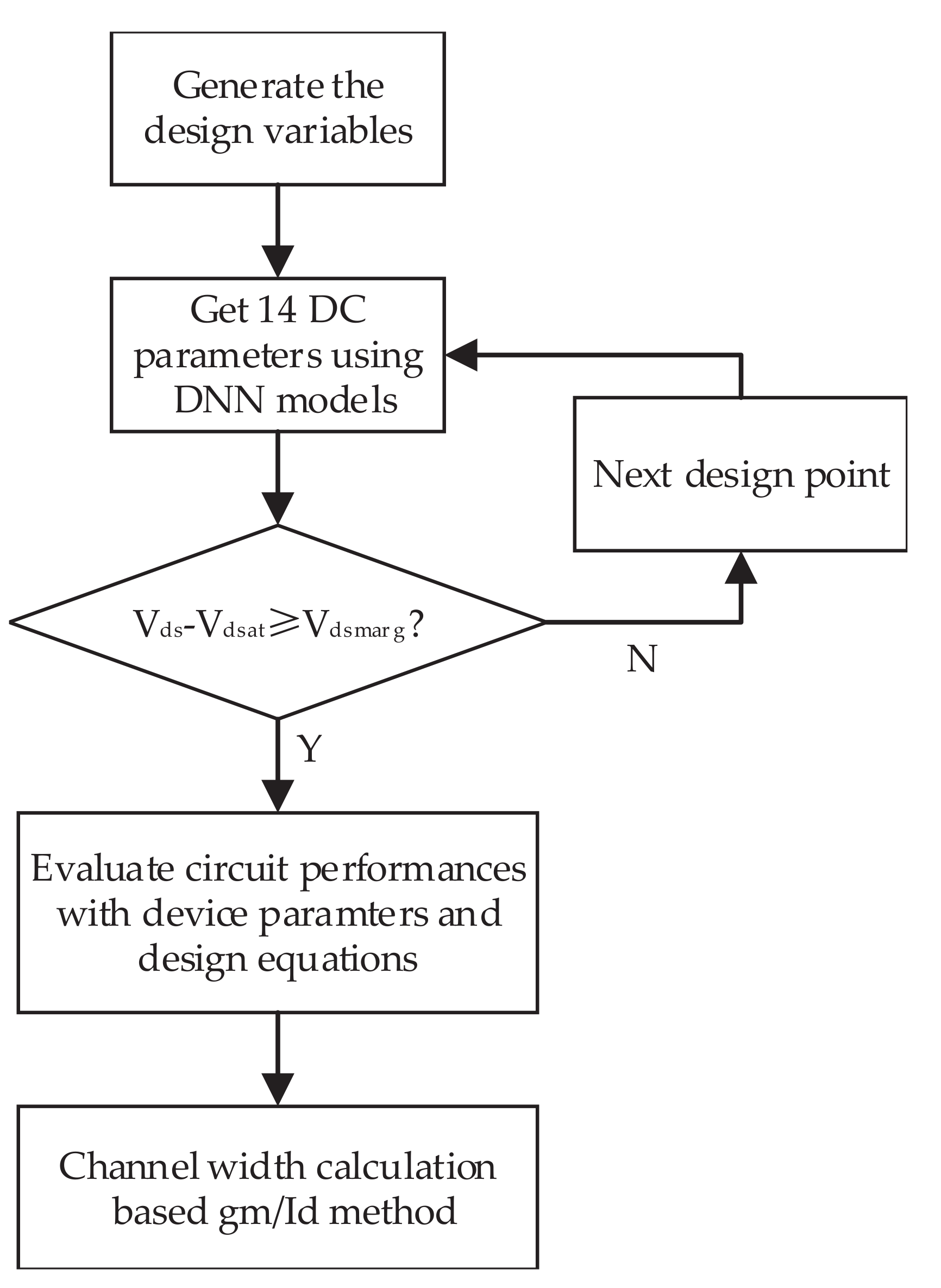
To ensure the efficacy of the design, this study incorporates a parameter known as voltage saturation margin (). This parameter determines whether a transistor operates in the saturation region by evaluating the condition . Any design point that includes transistors failing to satisfy the aforementioned condition is discarded. The working details of the parameter are shown in Figure 3.
The reuse of analog circuit designs represents a pivotal strategy for enhancing the efficiency of IC design. The approach employed in this paper for implementing circuit migration design is founded upon the design process outlined in Figure 2. Specifically, it entails leveraging distinct DNN models associated with different PDKs to generate the circuit design database corresponding to each respective PDK. Subsequently, the final device sizes are determined based on the performance requirements.
It is noteworthy that the methodology proposed in this paper involves traversing the design space and recurrent utilization of the DNN models for parameter prediction, which constitutes a significant portion of the overall process time. Consequently, the time-consuming nature of the model prediction phase holds great importance as it directly impacts the efficiency of circuit design database generation.
5. Results and Discussion
This section presents the performance of the proposed DNN models as well as experiments on circuit migration design. All experiments were performed on a Linux workstation with Intel(R) Xeon(R) Bronze 3204 CPU @ 1.90 GHz and 512 GB memory.
5.1. DNN Model Performance
5.1.1. The Comparison to Other ML Models
In order to demonstrate the superior performance of the proposed DNN models, a comparison is made with other ML models. The comparison encompasses traditional models such as Support Vector Regression, Ridge Regression, Bayesian Ridge, Decision Tree, Random Forest, and others [22,23,24,25,26], as well as more recent models such as TabNet, XGBoost, LightGBM, and Denominator Numerator Fit [27,28,29,30]. The evaluation metrics employed to assess the performance of these models are presented in Table 2.
Table 5 presents a comprehensive overview of the ML models employed for comparison. Notably, with the exception of the DNN models, which are multi-output, the remaining models are single-output models. Moreover, these single-output models utilize high-order features derived from feature generation as their input. In contrast to the DNN mode, these single-output models employ 116-dimensional high-order features to ensure optimal training. The feature generation process adheres to Algorithm A1, wherein the parameter settings are specified as order = 5 and overlap_order = 4.
In order to ensure a fair comparison of model performance, the training and inference processes were conducted using the Sklearn framework, with comprehensive evaluation performed across all models. Table 6 presents the performance results of these models on the test set, which comprised approximately 10,000 data points, specifically focusing on the prediction of the T65 NMOS transistor device parameter . Based on the evaluation metrics MAPE and MRE, the proposed DNN model outperforms all other models, with DNFit, BGR, DT, RF, XGBoost, BRR, RR, and TN models following in descending order. However, when considering the aspect of model size, the DNFit, BGR, DT, and RF models, despite exhibiting high accuracy, are notably larger compared to the proposed DNN model. In cases where all 14 parameters are taken into account, these models approach or surpass the size of LUTs. Nevertheless, after XGBoost, BRR, and TN models achieve all 14 parameter models, their total sizes either become comparable to that of the DNN model or their accuracy becomes less dominant. Regarding prediction time, when making approximately 10,000 predictions, the DNN model requires a total of 0.688 s. It is important to note that the DNN model outputs 14 parameters per prediction. From this perspective, considering an equivalent number of parameter predictions, the prediction time of the DNN model still exhibits commendable performance in both high-precision and low-storage occupation models.
To further demonstrate the superiority of the proposed multi-output DNN models, a performance comparison is conducted with single-output DNN models. Table 7 provides the hyperparameter settings for the single-output DNN models, while Table 8 presents the performance comparison between the single-output and multi-output DNN models in predicting the T65 NMOS parameter. In evaluating the results, it can be observed that the model size of the single-output DNN models and the multi-output DNN models are comparable, indicating that the multi-output model possesses an advantage in terms of model size. When considering all 14 parameters, the total size of the single-output model is 14 times that of a single model. Regarding prediction time, the time cost for predictions of the single-output model becomes similar to that of the multi-output model once the number of predicted parameters becomes equivalent. In terms of prediction results for the parameter, both the MRE and MAPE of the multi-output DNN models are smaller compared to the single-output DNN models. This indicates that the multi-output DNN models achieve higher accuracy in predicting the parameter.
Table 9 presents the MAPE and MRE results for all parameters of both the multi-output DNN and single-output DNN models across all PDKs. Overall, the prediction accuracy of the multi-output DNN models is comparable to that of the single-output DNN models. However, the multi-output DNN models demonstrate a distinct advantage in terms of storage space occupation, particularly in addressing the issue of large storage space consumption associated with lookup tables. The multi-output DNN models occupy a smaller storage space, making it more advantageous in mitigating the problem of substantial storage space occupation.
5.1.2. The Comparison to the LUTs
From the analysis of model size, the DNN models, including both NMOS and PMOS for each PDK, are 4.32 MB space. This size is significantly smaller compared to the storage space occupied by LUTs, which amounts to 1.4 GB space for T40 and T65, and 4.4 GB space for T180 and S180. The reduction rates in storage space achieved by the DNN models are 99.69% and 99.90%, respectively. In terms of prediction time analysis in Table 10, the average time consumed for a prediction by the LUTs is 0.00132 s, while the average prediction time for the DNN models is 0.00081 s. However, it is important to note that the DNN models predict 14 parameters, whereas the LUTs only have one parameter. When the time consumption is adjusted to account for all 14 prediction parameters, the DNN models reduce the time overhead by 95.62%. This clearly demonstrates the significant advantages of the DNN models in terms of speed.
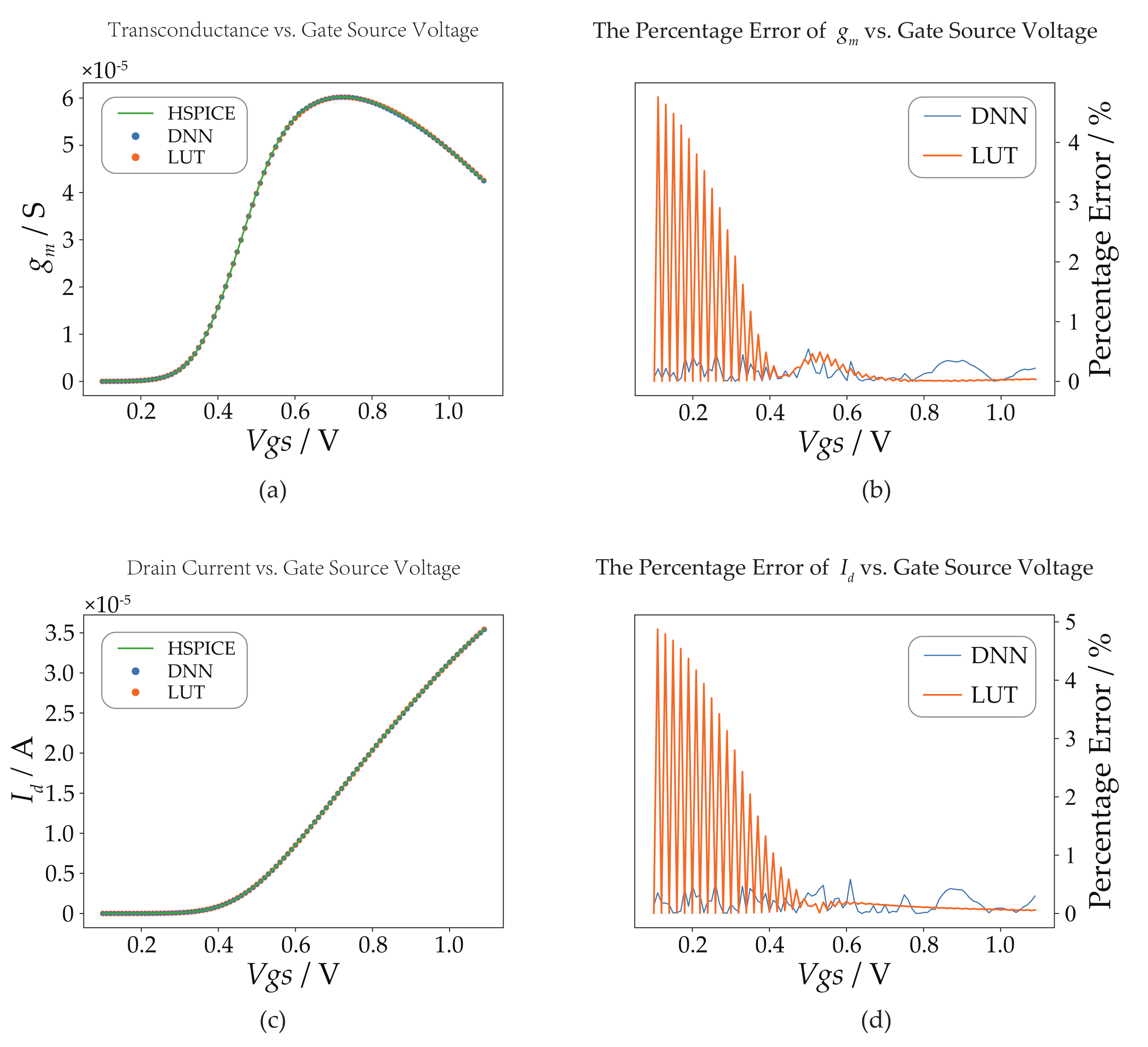
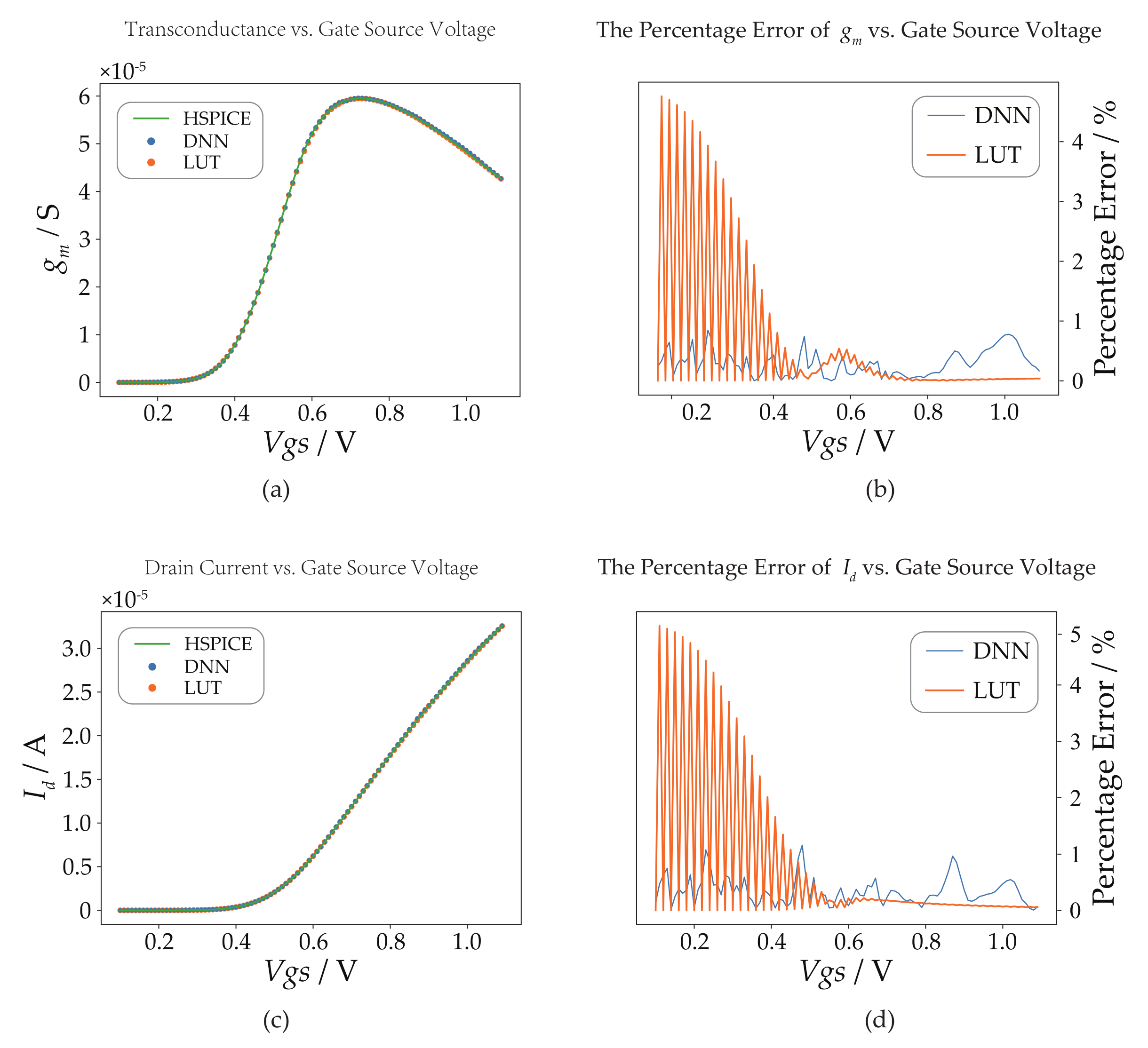
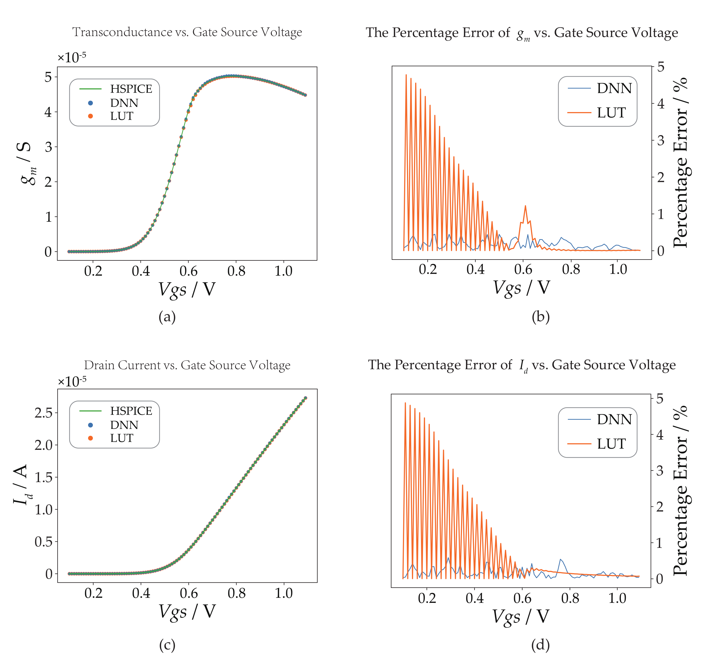
Moreover, to validate the accuracy of the DNN models, we conducted out-of-sample testing and compared its performance with that of the LUTs as well as the HSPICE (a simulator from Synopsys) results. Figure 4, Figure 5, Figure 6 and Figure 7 depict the accuracy of the DNN models in predicting the transistor parameters, specifically focusing on the parameters and for each technology. For the sake of simplicity, we present the results for these two parameters only. In the center subfigures, a comparison is made between the predictions of the DNN models and the LUTs, both of which are juxtaposed with the HSPICE results. On the other hand, the right subfigures illustrate the absolute percentage error of the DNN models and the LUTs relative to the HSPICE results. By analyzing the percentage error comparison, it is evident that the DNN models exhibit a maximum percentage error of less than 2% and an absolute average percentage error of approximately 1%. These results highlight the superior performance of the DNN models over the LUTs, which rely on linear interpolation, particularly in terms of the average percentage error in parameter prediction. Furthermore, the percentage error curves of the LUTs demonstrate a sawtooth pattern with gradually decreasing peak values in regions where the parameter value changes significantly. In contrast, the percentage error curve of the DNN models exhibits less fluctuation and greater randomness, indicating its more stable prediction performance.
5.2. Circuit Migration Design
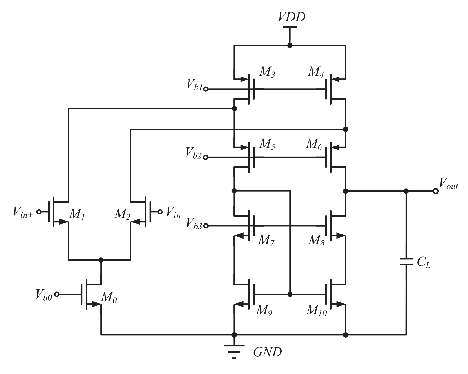
5.2.1. Folded Cascode Operation Amplifier (FC OPAMP)
The FC OPAMP is shown in Figure 8. Table 11 presents the specification requirements of FC OPAMP for T40, T65, T180, and S180. Equation (2) shows the design equations of the FC OPAMP, while Table 12 provides the range of each transistor design variable for the FC OPAMP. For this specific example, the value of is set at 50 mV, while the value of is set to 1.05.
In this case, by employing DNN models for circuit design, the database comprising approximately 780,000 design points requires approximately 92 s for generation for each technology, whereas the utilization of LUTs necessitates approximately 155 s. Compared with using LUTs, using DNN models can shorten the time consumption by 40.65%. This implies that in practical design applications, DNN models are still capable of maintaining a speed advantage.
Table 13, Table 14 and Table 15 display the sizing results, pre-simulation results, and post-simulation results of the FC OPAMP in T40, T65, T180, and S180, respectively. The results demonstrate two key observations. Firstly, the circuit simulation results in all four technologies meet the specified requirements, validating the effectiveness of the proposed circuit migration design method. Secondly, it is noteworthy that, for comparable simulation outcomes, the transistor size required in T40 exceeds that of T65, while the sizing results between T180 and S180 are more similar. This observation suggests that it is more challenging to realize this circuit in T40.
where G = , = , = .
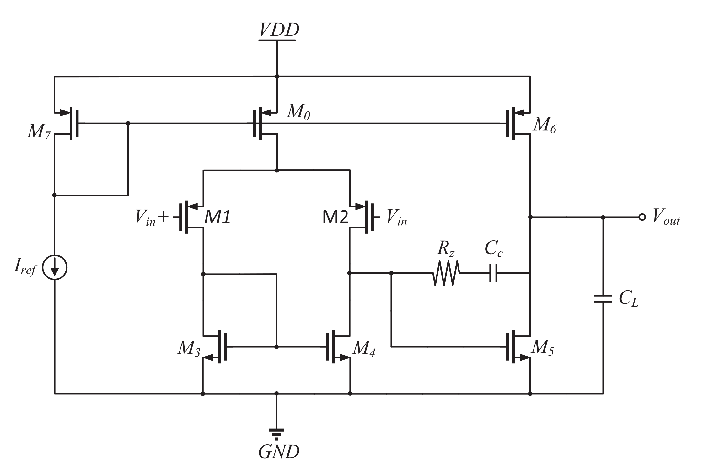
5.2.2. Miller Operation Amplifier(MI OPAMP)
The MI OPAMP is shown in Figure 9. The specification requirements of MI OPAMP for T40, T65, T180, and S180 are presented in Table 16. The design equations of the MI OPAMP are provided in Equation (3), while the range of each device design variable for MI OPAMP is specified in Table 17. It is worth noting that the values of M5, M6, and M7 in the MI OPAMP are influenced by the of M3 and M0, and therefore, there is no need to restrict the range of M5, M6, and M7. The saturation voltage margin parameter, , is set to 50 mV in this particular example.
In the context of this circuit design case, it has been observed that the generation of a database consisting of approximately one million design points through the utilization of the DNN models takes roughly 120 s, whereas the same task requires approximately 210 s when utilizing LUTs. This represents a 42.86% reduction in the time overhead, as compared to the LUTs approach.
Table 18, Table 19 and Table 20 display the sizing results, pre-simulation results, and post-simulation results of the MI OPAMP in T40, T65, T180, and S180, respectively. The results indicate that the circuit simulation results in all four PDKs satisfying the specified requirements, thus demonstrating the effectiveness of the proposed method. Furthermore, consistent with the sizing results of the FC OPAMP, it is observed that the results for T180 and S180 exhibit relatively close values. However, in order to meet the specification requirements, T40 demands larger device sizes and RC values compared to T65.
where , =, = .
6. Conclusions
This paper presents a novel approach for training DNN models to replace the LUTs in the method, thereby significantly reducing storage space requirements. The proposed method focuses on training DNN models for NMOS and PMOS device parameters in prevalent IC design technologies, namely T40, T65, T180, and S180. By employing DNN models, the storage space requirements can be reduced by at least 99% compared to LUTs. Furthermore, the DNN models demonstrate high prediction accuracy, with an average percentage error of less than 1%. In terms of prediction time, the DNN models outperform LUTs by reducing the time overhead by 91.46% when predicting an equivalent number of parameters.
Additionally, this paper introduces an automated porting design approach for analog circuits that combines the DNN models with the design method. The objective is to facilitate circuit design reuse across different technologies. The proposed method is validated through migration design experiments involving folded cascode amplifiers and Miller two-stage amplifiers in the mainstream technologies of T40, T65, T180, and S180. The experimental results demonstrate that utilizing the DNN models can reduce the time overhead by 40% compared to using LUTs. Furthermore, the pre- and post-simulation results of the circuit confirm that the proposed method enables the automated design of circuits with identical specifications across different technologies.
Based on the experimental results, it was observed that to achieve the same performance specifications, the sizing of operational amplifiers in T40 technology is relatively larger than that of T65 technology for both circuit architectures. Therefore, it is recommended that for advanced technology circuit design, the performance targets can be relaxed to obtain smaller circuit sizes. Alternatively, one may consider replacing the architecture to meet the desired specifications.
Author Contributions
Q.W. and H.L. conducted the experiments and coordinated the experiments. H.L. and J.X. proposed the model. Q.W. and H.L. prepared the first draft of the manuscript. L.L., Z.Y., and Y.W. commented on the manuscript. L.L. supervised the project. All authors have read and agreed to the published version of the manuscript.
Funding
This work is supported by the National Key Research and Development Project under Grant No. 2019YFB2205001.
Data Availability Statement
The experimental results of all PDK models are available from https://github.com/liuhaixu2021 (accessed on 28 May 2023), the original data pickle file is approximately 31.54 GB, and due to Github’s restriction on uploading files larger than 100 MB, we have placed a permanent download link to the full data in a markdown file in Github.
Conflicts of Interest
The authors declare no conflict of interest.
Abbreviations
The following abbreviations are used in this manuscript:
| CMOS | complementary metal-oxide-semiconductor |
| DC | direct-current |
| DNN | deep neural network |
| FC OPAMP | folded cascode operation amplifier |
| IC | integrated circuit |
| ISRU | inverse square root unit |
| KVL | Kirchhoff’s voltage law |
| LUT | lookup table |
| MAPE | mean absolute percentage error |
| ML | machine learning |
| MRE | maximum relative error |
| MI OPAMP | miller operation amplifier |
| NMOS | negative channel metal-oxide-semiconductor |
| PDK | process design kit |
| PMOS | positive channel metal-oxide-semiconductor |
| ReLU | rectified linear unit |
| SPICE | simulation program with integrated circuit emphasis |
| S180 | SMIC 180 nm |
| T40 | TSMC 40 nm |
| T65 | TSMC 65 nm |
| T180 | TSMC 180 nm |
| DC loop gain | |
| common mode rejection | |
| gain-band width | |
| phase margin | |
| resistor-capacitor | |
| slew rate |
Appendix A. Deep Neural Networks Algorithm
The relevant algorithms of the deep neural network are as follows, Algorithm A1 is the feature generation algorithm, Algorithm A2 is the deep neural network training algorithm, and Algorithm A3 is the deep neural network prediction algorithm.
| Algorithm A1 Feature Generation |
|
| Algorithm A2 DNN Model Training |
|
| Algorithm A3 DNN Model Prediction |
|
References
- Uhlmann, Y.; Brunner, M.; Bramlage, L.; Scheible, J.; Curio, C. Procedural- and Reinforcement-Learning-Based Automation Methods for Analog Integrated Circuit Sizing in the Electrical Design Space. Electronics 2023, 12, 302. [Google Scholar] [CrossRef]
- Gielen, G.G.E. CAD tools for embedded analogue circuits in mixed-signal integrated systems on chip. IEEE Proc.-Comput. Digit. Tech. 2005, 152, 317–332. [Google Scholar] [CrossRef]
- Liu, B.; Fernández, F.V.; Gielen, G.; Castro-López, R.; Roca, E. A memetic approach to the automatic design of high-performance analog integrated circuits. ACM Trans. Des. Autom. Electron. Syst. (TODAES) 2009, 14, 1–24. [Google Scholar] [CrossRef]
- Scheible, J. Optimized is Not Always Optimal. In Proceedings of the 2022 Symposium on International Symposium on Physical Design (ISPD ’22), Virtual Event, 27–30 March 2022; pp. 151–158. [Google Scholar] [CrossRef]
- Silveira, F.; Flandre, D.; Jespers, P.G.A. A gm/ID based methodology for the design of CMOS analog circuits and its application to the synthesis of a silicon-on-insulator micropower OTA. IEEE J.-Solid-State Circuits 1996, 31, 1314–1319. [Google Scholar] [CrossRef]
- Jespers, P.; Murmann, B. Systematic Design of Analog CMOS Circuits Using Pre-Computed Lookup Tables; Cambridge University Press: Cambridge, UK, 2017. [Google Scholar] [CrossRef]
- Kumar, T.B.; Sharma, G.K.; Johar, A.K.; Gupta, D.; Kar, S.K.; Boolchandani, D. Design Automation of 5-T OTA using gm/ID methodology. In Proceedings of the 2019 IEEE Conference on Information and Communication Technology, Allahabad, India, 6–8 December 2019; pp. 1–5. [Google Scholar] [CrossRef]
- Shi, G. Sizing of multi-stage Op Amps by combining design equations with the gm/ID method. Integration 2021, 79, 48–60. [Google Scholar] [CrossRef]
- Omran, H.; Amer, M.H.; Mansour, A.M. Systematic design of bandgap voltage reference using precomputed lookup tables. IEEE Access 2019, 7, 100131–100142. [Google Scholar] [CrossRef]
- Elmeligy, K.; Omran, H. Fast design space exploration and multi-objective optimization of wide-band noise-canceling LNAs. Electronics 2022, 11, 816. [Google Scholar] [CrossRef]
- Gebreyohannes, F.T.; Porte, J.; Louërat, M.M.; Aboushady, H. A gm/ID methodology based data-driven search algorithm for the design of multistage multipath feed-forward-compensated amplifiers targeting high speed continuous-time ∑Δ-modulators. IEEE Trans.-Comput.-Aided Des. Integr. Circuits Syst. 2020, 39, 4311–4324. [Google Scholar] [CrossRef]
- Youssef, A.A.; Murmann, B.; Omran, H. Analog IC Design Using Precomputed Lookup Tables: Challenges and Solutions. IEEE Access 2020, 8, 134640–134652. [Google Scholar] [CrossRef]
- Habal, H.; Tsonev, D.; Schweikardt, M. Compact models for initial MOSFET sizing based on higher-order artificial neural networks. In Proceedings of the 2020 ACM/IEEE Workshop on Machine Learning for CAD, Virtual Event, 16–20 November 2020; pp. 111–116. [Google Scholar] [CrossRef]
- Yang, Z.K.; Hsu, M.H.; Chang, C.Y.; Ho, Y.W.; Liu, P.N.; Lin, A. Circuit convergence study using machine learning compact models. engrxiv 2021. [Google Scholar] [CrossRef]
- Ho, Y.W.; Rawat, T.S.; Yang, Z.K.; Pratik, S.; Lai, G.W.; Tu, Y.L.; Lin, A. Neuroevolution-based efficient field effect transistor compact device models. IEEE Access 2021, 9, 159048–159058. [Google Scholar] [CrossRef]
- Wang, Y.; Xin, J.; Liu, H.; Qin, Q.; Chai, C.; Lu, Y.; Hao, J.; Xiao, J.; Ye, Z.; Wang, Y. DC-Model: A New Method for Assisting the Analog Circuit Optimization. In Proceedings of the 2023 24th International Symposium on Quality Electronic Design (ISQED), San Francisco, CA, USA, 5–7 April 2023; pp. 1–7. [Google Scholar] [CrossRef]
- Qi, G.; Chen, X.; Hu, G.; Zhou, P.; Bao, W.; Lu, Y. Knowledge-based neural network SPICE modeling for MOSFETs and its application on 2D material field-effect transistors. Inf. Sci. 2023, 66, 122405:1–122405:10. [Google Scholar] [CrossRef]
- Wang, Q.; Ye, M.; Li, Y.; Zheng, X.; He, J.; Du, J.; Zhao, Y. MOSFET modeling of 0.18 μm CMOS technology at 4.2 K using BP neural network. Microelectron. J. 2023, 132, 105678. [Google Scholar] [CrossRef]
- Fu, L.; Wang, F. The performance prediction model of NMOSFET based on BP neural network. In Proceedings of the Third International Conference on Sensors and Information Technology (ICSI 2023), Xiamen, China, 6–8 January 2023; pp. 162–169. [Google Scholar] [CrossRef]
- Wei, J.; Zhao, T.; Zhang, Z.; Wan, J. Modeling of CMOS transistors from 0.18 μm process by artificial neural network. Integration 2022, 87, 11–15. [Google Scholar] [CrossRef]
- Glorot, X.; Bordes, A.; Bengio, Y. Deep Sparse Rectifier Neural Networks. In Proceedings of the Fourteenth International Conference on Artificial Intelligence and Statistics, Proceedings of Machine Learning Research, Fort Lauderdale, FL, USA, 11–13 April 2011; Gordon, G., Dunson, D., Dudík, M., Eds.; PMLR: Fort Lauderdale, FL, USA, 2011; Volume 15, pp. 315–323. Available online: https://proceedings.mlr.press/v15/glorot11a.html (accessed on 13 February 2022).
- Hearst, M.A.; Dumais, S.T.; Osuna, E.; Platt, J.; Scholkopf, B. Support vector machines. IEEE Intell. Syst. Their Appl. 1998, 13, 18–28. [Google Scholar] [CrossRef] [Green Version]
- Webb, G.I.; Boughton, J.R.; Wang, Z. Not so naive Bayes: Aggregating one-dependence estimators. Mach. Learn. 2005, 58, 5–24. [Google Scholar] [CrossRef] [Green Version]
- Breiman, L. Random forests. Mach. Learn. 2001, 45, 5–32. [Google Scholar] [CrossRef] [Green Version]
- Quinlan, J.R. Induction of decision trees. Mach. Learn. 1986, 1, 81–106. [Google Scholar] [CrossRef] [Green Version]
- Quinlan, J.R. C4.5: Programs for Machine Learning; Morgan Kaufmann Publishers Inc.: San Francisco, CA, USA, 1993. [Google Scholar]
- Arik, S.Ö.; Pfister, T. Tabnet: Attentive interpretable tabular learning. In Proceedings of the AAAI Conference on Artificial Intelligence, Virtual Event, 2–9 February 2021; pp. 6679–6687. [Google Scholar] [CrossRef]
- Chen, T.; Guestrin, C. Xgboost: A scalable tree boosting system. In Proceedings of the 22nd ACM Sigkdd International Conference on Knowledge Discovery and Data Mining, Long Beach, CA, USA, 13–17 August 2016; pp. 785–794. [Google Scholar] [CrossRef] [Green Version]
- Ke, G.; Meng, Q.; Finley, T.; Wang, T.; Chen, W.; Ma, W.; Liu, T.Y. Lightgbm: A highly efficient gradient boosting decision tree. In Proceedings of the 31st International Conference on Neural Information Processing Systems, Red Hook, NY, USA, 4–9 December 2017; pp. 3149–3157. [Google Scholar] [CrossRef]
- Hu, W.; Ma, D.; Pan, Z.; Ye, Z.; Wang, Y. DNFIT Based Curve Fitting And Prediction In Semiconductor Modeling And Simulation. In Proceedings of the 2019 International Conference on IC Design and Technology (ICICDT), Suzhou, China, 17–19 June 2019; pp. 1–4. [Google Scholar] [CrossRef]
Figure 1.
Model architecture.

Figure 2.
The design flow of the proposed sizing method.

Figure 3.
The working details of the parameter.

Figure 4.
DNN model (NMOS) compared to the LUT and HSPICE in T40 for L = 1 µm, = 0.6 V and = 0 V. (a) -versus- curves. (b) The absolute percentage error curve of DNN and LUT relative to HSPICE for . (c) -versus- curves. (d) The absolute percentage error curve of DNN and LUT relative to HSPICE for .
Figure 4.
DNN model (NMOS) compared to the LUT and HSPICE in T40 for L = 1 µm, = 0.6 V and = 0 V. (a) -versus- curves. (b) The absolute percentage error curve of DNN and LUT relative to HSPICE for . (c) -versus- curves. (d) The absolute percentage error curve of DNN and LUT relative to HSPICE for .

Figure 5.
DNN model (NMOS) compared to the LUT and HSPICE in T65 for L = 1 µm, = 0.6 V, and = 0 V. (a) -versus- curves. (b) The absolute percentage error curve of DNN and LUT relative to HSPICE for . (c) -versus- curves. (d) The absolute percentage error curve of DNN and LUT relative to HSPICE for .

Figure 6.
DNN model (NMOS) compared to the LUT and HSPICE in T180 for L = 1 µm, = 0.6 V, and = 0 V. (a) -versus- curves. (b) The absolute percentage error curve of DNN and LUT relative to HSPICE for . (c) -versus- curves. (d) The absolute percentage error curve of DNN and LUT relative to HSPICE for .

Figure 7.
DNN model (NMOS) compared to the LUT and HSPICE in S180 for L = 1 µm, = 0.6 V, and = 0 V. (a) -versus- curves. (b) The absolute percentage error curve of DNN and LUT relative to HSPICE for . (c) -versus- curves. (d) The absolute percentage error curve of DNN and LUT relative to HSPICE for .

Figure 8.
Folded cascode operation amplifier (FC OPAMP).

Figure 9.
Miller operational amplifier (MI OPAMP).


Table 1.
The hyperparameter settings of DNN.
| Name | Value |
|---|---|
| Input layer dimensions | 74 |
| Number of hidden layers | 6 |
| Hidden layer dimension | (150,120,120,120,120,150) |
| Output layer dimensions | 14 |
| Activation function | ReLU |
| Learning rate | |
| Loss function | MSE |
| Training epochs | 1000 |
| Optimizer | Adam |
| Tolerance | |
| Batch size | 256 |
Table 2.
The metrics and statements of the DNN models.
| No. | Metric | Satement |
|---|---|---|
| 1 | Size | The storage capacity utilized by the model |
| 2 | Time | The average inference time consumed by the model for one prediction |
| 3 | MAPE | The mean absolute percentage error between the predicted value and the true value |
| 4 | MRE | The maximum relative error between the predicted value and the true value |
Table 3.
The , , , L range and step size of transistors each PDK on the dataset.
| Name | T40 | T65 | T180 | S180 | Unit |
|---|---|---|---|---|---|
| W | 5 | 5 | 5 | 5 | µm |
| 0.1–1.2 | 0.1–1.2 | 0.1–1.8 | 0.1–1.8 | V | |
| 0.1–1.2 | 0.1–1.2 | 0.1–1.8 | 0.1–1.8 | V | |
| 0–1.2 | 0–1.2 | 0–1.8 | 0–1.8 | V | |
| L | 0.5–6 | 0.5–6 | 0.5–6 | 0.5–6 | µm |
The values in this table are absolute values.
Table 4.
The size and the including parameters of the dataset according to Table 3.
Table 4.
The size and the including parameters of the dataset according to Table 3.
| PDK | Size | Parameter |
|---|---|---|
| T40 | 1.4 GB | , , , , , , , , , , , , , and |
| T65 | ||
| T180 | 4.4 GB | |
| S180 |
Size: including PMOS and NMOS.
Table 5.
The ML models for comparison.
| No. | Acronym | Full Name |
|---|---|---|
| 1 | ABR | AdaBoost Regressor |
| 2 | BGR | Bagging Regressor |
| 3 | BRR | Bayesian Ridge Regression |
| 4 | DNFit | Denominator Numerator Fit |
| 5 | DNN | Deep Neural Networks |
| 6 | DT | Decision Tree |
| 7 | EN | ElasticNet |
| 8 | GBR | Gradient Boosting Regressor |
| 9 | KNN | K-Nearest Neighbors |
| 10 | LASSO | Least Absolute Shrinkage and Selection Operator |
| 11 | LARS | Least Angle Regression |
| 12 | LL | LassoLars |
| 13 | LGBM | Light Gradient Boosting Machine |
| 14 | PAR | Passive Aggressive Regressor |
| 15 | PLSR | Partial Least Squares Regression |
| 16 | RF | Random Forest |
| 17 | RR | Ridge Regression |
| 18 | SVR | Support Vector Regression |
| 19 | TN | TabNet |
| 20 | XGBoost | Extreme Gradient Boosting |
Table 6.
The performance of different ML models for parameter on the test set.
| No. | Model Name | Total Time(s) | Size(KB) | MRE | MAPE |
|---|---|---|---|---|---|
| 1 | DNN | 0.668 | 2160 | 0.0228 | 0.00191 |
| 2 | DNFit | 0.0176 | 76,421 | 0.09 | 0.007 |
| 3 | BGR | 2.54 | 4,059,874 | 0.09 | 0.009 |
| 4 | DT | 0.00295 | 10158 | 0.16 | 0.009 |
| 5 | RF | 0.202 | 642,238 | 0.10 | 0.006 |
| 6 | XGBoost | 0.0105 | 730 | 0.12 | 0.019 |
| 7 | BRR | 0.00661 | 110 | 0.16 | 0.026 |
| 8 | RR | 0.00288 | 1.48 | 0.18 | 0.026 |
| 9 | TN | 0.101 | 495 | 0.45 | 0.061 |
| 10 | GBR | 0.0130 | 175.1 | 0.44 | 0.067 |
| 11 | PAR | 0.00148 | 1.73 | 0.42 | 0.108 |
| 12 | ABR | 0.0544 | 61 | 2.78 | 0.411 |
| 13 | KNN | 11.7 | 7491.1 | 14.59 | 0.145 |
| 14 | LL | 0.00123 | 2.56 | 23,963.87 | 259.37 |
| 15 | LASSO | 0.00178 | 1.56 | 223.35 | 8.28 |
| 16 | LARS | 0.000850 | 127.31 | 352,261.34 | 230.09 |
| 17 | EN | 0.00474 | 1.57 | 104.86 | 4.910 |
| 18 | SVR | 1.06 | 2079.36 | 32.77 | 0.17 |
| 19 | LGBM | 0.0102 | 69.05 | 54.99 | 2.03 |
| 20 | PLSR | 0.00486 | 2548.77 | 199.57 | 1.49 |
Table 7.
The hyperparameters settings of single-output DNN.
| Name | Value |
|---|---|
| Input layer dimensions | 116 |
| Number of hidden layers | 5 |
| Hidden layer dimension | (110,100,100,100,110) |
| Output layer dimensions | 1 |
| Activation function | ReLU |
| Learning rate | |
| Loss function | MSE |
| Training epochs | 1000 |
| Optimizer | Adam |
| Tolerance | |
| Batch size | 256 |
Table 8.
The performance comparison between multi-output and single-output DNN models on T65 NMOS parameter on the test set.
Table 8.
The performance comparison between multi-output and single-output DNN models on T65 NMOS parameter on the test set.
| Name | Total Time (s) | Size (KB) | MRE | MAPE |
|---|---|---|---|---|
| Multi-output DNN | 0.6680 | 2160 | 0.0228 | 0.00191 |
| Single-output DNN | 0.0353 | 2302 | 0.0332 | 0.00297 |
Table 9.
The MRE and MAPE results of DNN models between multi-output and single-output on the test set.
Table 9.
The MRE and MAPE results of DNN models between multi-output and single-output on the test set.
| PDK | Device | Parameters | Multi-Output | Single-Output | ||
|---|---|---|---|---|---|---|
| MAPE | MRE | MAPE | MRE | |||
| T65 | NMOS | |||||
| PMOS | ||||||
| T40 | NMOS | |||||
| PMOS | ||||||
| T180 | NMOS | |||||
| PMOS | ||||||
| S180 | NMOS | |||||
| PMOS | ||||||
Table 10.
The comparison of time performance between LUTs and DNN models.
| Scale of Data (The Exponent of 10) | Time (s) | |
|---|---|---|
| DNN Models | LUTs | |
| 0 | 0.00081 | 0.00132 |
| 1 | 0.00366 | 0.00113 |
| 2 | 0.00747 | 0.00169 |
| 3 | 0.05834 | 0.00487 |
| 4 | 0.29765 | 0.03070 |
Table 11.
Specification for FC OPAMP in T40, T65, T180, and S180 technologies.
| Parameter | Unit | Specification (T40 and T65) | Specification (T180 and S180) |
|---|---|---|---|
| V | 1.2 | 1.8 | |
| pF | 5 | 2 | |
| DC loop gain () | dB | ≥55 | ≥65 |
| Gain-band width () | MHz | ≥ 20 | ≥50 |
| Phase margin () | ≥60 | ≥60 | |
| Common mode rejection ratio () | dB | ≥70 | ≥80 |
| Slew rate () | V/us | ≥ 10 | ≥20 |
| Area | µm | minimum | minimum |
Table 12.
The design variable of each transistor in FC OPAMP.
| Parameter | Unit | Min | Max |
|---|---|---|---|
| S/A | 10 | 15 | |
| S/A | 15 | 27 | |
| S/A | 12 | 17 | |
| S/A | 12 | 17 | |
| S/A | 12 | 17 | |
| S/A | 12 | 17 | |
| L | µm | 0.5 | 2.5 |
Table 13.
List of device sizes of the FC OPAMP.
| Parameter | Unit | T40 | T65 | T180 | S180 |
|---|---|---|---|---|---|
| µm/µm | 10.4/0.5 | 37.6/0.5 | 12.8/0.5 | 10.4/0.5 | |
| µm/µm | 112/1.1 | 84.6/0.5 | 73/0.8 | 43/0.8 | |
| µm/µm | 124/1.1 | 39.2/0.5 | 11.2/0.8 | 4.2/0.8 | |
| µm/µm | 140.8/1.1 | 41/0.5 | 16/0.8 | 5.8/0.8 | |
| µm/µm | 30.4/1.1 | 15.2/0.5 | 32/0.8 | 24/0.8 | |
| µm/µm | 22.8/1.1 | 10.8/0.5 | 17.2/0.8 | 16/0.8 |
Table 14.
Pre-simulation results of FC OPAMP.
| Parameter | Unit | T40 | T65 | T180 | S180 |
|---|---|---|---|---|---|
| dB | 55.3 | 59.2 | 69.5 | 69.8 | |
| MHz | 22.6 | 24.1 | 53.4 | 54.5 | |
| 71.9 | 85.6 | 73.6 | 68.6 | ||
| dB | 88.6 | 115.6 | 103.3 | 118.5 | |
| V/us | 11.3 | 13.2 | 35.1 | 26.5 | |
| area | µm | 951.2 | 209.6 | 243.8 | 159.1 |
Table 15.
Post-simulation results of FC OPAMP.
| Parameter | Unit | T40 | T65 | T180 | S180 |
|---|---|---|---|---|---|
| dB | 55.0 | 58.6 | 68.2 | 69.4 | |
| MHz | 20.9 | 22.5 | 51.5 | 52.1 | |
| 65.5 | 83.8 | 76.8 | 79.0 | ||
| dB | 72.1 | 82.9 | 93.5 | 98.1 | |
| V/µs | 10.4 | 12.5 | 26.9 | 24.7 |
Table 16.
The specification of MI OPAMP for T40, T65, T180, and S180 technologies.
| Parameter | Unit | Specification (T40 and T65) | Specification (T180 and S180) |
|---|---|---|---|
| V | 1.2 | 1.8 | |
| pF | 5 | 5 | |
| dB | ≥60 | ≥72 | |
| MHz | ≥25 | ≥30 | |
| ≥60 | ≥60 | ||
| dB | ≥50 | ≥70 | |
| V/us | ≥ 10 | ≥15 | |
| area | µm | minimum | minimum |
Table 17.
The design variable of each device in MI OPAMP.
| Parameter | Unit | Min | Max |
|---|---|---|---|
| S/A | 10 | 15 | |
| S/A | 15 | 27 | |
| S/A | 10 | 15 | |
| L | µm | 0.5 | 2.5 |
| pF | 1 | 2 | |
| 1000 | 5000 |
Table 18.
List of device sizes of the MI OPAMP.
| Parameter | Unit | T40 | T65 | T180 | S180 |
|---|---|---|---|---|---|
| µm/µm | 17.6/0.5 | 15/0.5 | 28/0.5 | 27/0.5 | |
| µm/µm | 312/2 | 82.8/0.5 | 46/0.5 | 38.4/0.5 | |
| µm/µm | 10.4/2.3 | 1.6/0.5 | 3.2/0.5 | 2.7/0.5 | |
| µm/µm | 70/1.4 | 17.6/0.5 | 36/0.5 | 29.4/0.5 | |
| µm/µm | 214.2/2.3 | 128/1.1 | 221/0.5 | 126/0.5 | |
| µm/µm | 4.4/0.5 | 6/0.5 | 7/0.5 | 6/0.5 | |
| pF | 1.75 | 1.5 | 1.5 | 1.5 | |
| k | 2 | 1.6 | 1.1 | 1.2 |
Table 19.
Pre-simulation results of MI OPAMP.
| Parameter | Unit | T40 | T65 | T180 | S180 |
|---|---|---|---|---|---|
| dB | 62.0 | 64.8 | 76.0 | 76.1 | |
| MHz | 31.8 | 28.1 | 32.3 | 35.1 | |
| 84.3 | 64.5 | 73.2 | 72.2 | ||
| dB | 53.5 | 54.2 | 77.2 | 76.9 | |
| V/us | 23.9 | 14.2 | 20.8 | 23.3 | |
| area | µm | 1895.3 | 241.5 | 258 | 132.3 |
Table 20.
Post-simulation results of MI OPAMP.
| Parameter | Unit | T40 | T65 | T180 | S180 |
|---|---|---|---|---|---|
| dB | 61.5 | 63.6 | 75.4 | 74.9 | |
| MHz | 29.4 | 27.7 | 31.8 | 33.7 | |
| ° | 81.7 | 64.7 | 64.7 | 69.6 | |
| dB | 52.9 | 53.6 | 75.2 | 74.5 | |
| V/µs | 21.7 | 13.8 | 20.1 | 22.4 |
Disclaimer/Publisher’s Note: The statements, opinions and data contained in all publications are solely those of the individual author(s) and contributor(s) and not of MDPI and/or the editor(s). MDPI and/or the editor(s) disclaim responsibility for any injury to people or property resulting from any ideas, methods, instructions or products referred to in the content. |
© 2023 by the authors. Licensee MDPI, Basel, Switzerland. This article is an open access article distributed under the terms and conditions of the Creative Commons Attribution (CC BY) license (https://creativecommons.org/licenses/by/4.0/).
Share and Cite
MDPI and ACS Style
Wu, Q.; Liu, H.; Xin, J.; Li, L.; Ye, Z.; Wang, Y. Deep Neural Networks-Based Direct-Current Operation Prediction and Circuit Migration Design. Electronics 2023, 12, 2780. https://doi.org/10.3390/electronics12132780
AMA Style
Wu Q, Liu H, Xin J, Li L, Ye Z, Wang Y. Deep Neural Networks-Based Direct-Current Operation Prediction and Circuit Migration Design. Electronics. 2023; 12(13):2780. https://doi.org/10.3390/electronics12132780
Chicago/Turabian StyleWu, Qingsen, Haixu Liu, Jian Xin, Lin Li, Zuochang Ye, and Yan Wang. 2023. "Deep Neural Networks-Based Direct-Current Operation Prediction and Circuit Migration Design" Electronics 12, no. 13: 2780. https://doi.org/10.3390/electronics12132780
Note that from the first issue of 2016, this journal uses article numbers instead of page numbers. See further details here.