1. Introduction
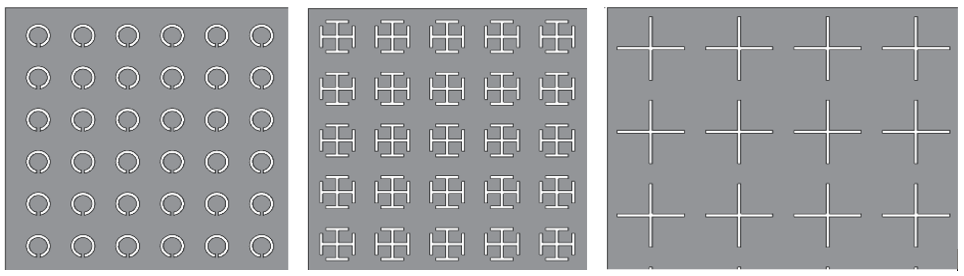
A metamaterial (MM) is an artificial material/device consisting of an array of sub-wavelength-size structural elements (shown in
Figure 1) that can take on the properties of non-naturally occurring materials [
1]. It can be more specifically described as a
ε-negative (ENG) or
µ-negative (MNG) material of either negative permittivity or permeability, respectively, a double-negative (DNG) when both of these quantities are simultaneously negative in a particular frequency range, and
ε-near-zero (ENZ) or a
µ-near-zero (MNZ) material with small, close-to-zero values for these quantities (this might be the case when the materials are close to their electric or magnetic plasma frequency) [
2]. This creates new opportunities to interact with electromagnetic waves (from microwave band to visible light) and mechanical (ultrasonic) waves. In this paper, we will focus on electromagnetic waves in the terahertz frequency band. In this case, various field transformations of arbitrary incident fields can be achieved. Planar versions of MM-metasurfaces (MS) are much easier to fabricate (in comparison to 3D structures) and can potentially have many applications. The first of the areas in which metasurfaces can be used is telecommunications. Among other things, it can be used to improve the efficiency of antennas by increasing directivity, increasing power gain, increasing selectivity, or by multiplexing signals [
3,
4,
5,
6]. Other peripheral areas for metasurfaces are selective absorbing structures [
7,
8], polarizers [
9,
10], surface wave control devices [
11,
12], wave front manipulation devices [
13,
14] and imaging systems (for lensing electromagnetic waves) [
15,
16]. Particularly noteworthy are works showing plasmonic metasurfaces used as perfect absorbers and pulse controllers [
17,
18]. Other peripheral areas for metasurfaces are measurement systems. Among the most frequently mentioned are applications for evaluating biological samples, where it is most often indicated in the detection of biomolecules, microorganisms, cancer, or tumors [
19]. Other applications include testing chemicals and measuring strain [
20,
21]. Exemplary metasurface structures are presented in
Figure 1.
Characterization of the fabrication process uncertainty is a key question for quality control. So far, the effect of changing the geometry of the metasurface created by inaccuracies in the fabrication process has been studied for different dimensions of rectangular structural elements in the work [
22]. In our work, we investigated the effect of the fabrication process on the operation of SRR-based meta-surfaces; it is a more complicated structure to analyze because as a result of the process, some dimensions increase (gap width and distances between elements) and some decrease (line width and size of the square loop) as a result of over-etching. In our work, the effect of not only changing the geometry as a result of the etching process but also of oxidation and metallization was studied. The paper [
22] studied the effect of the fabrication process on the metasurface in a hologram application, where the effect of fabrication on the phase of the electromagnetic wave was examined. In this paper, the effect of the fabrication process on resonances was studied, as we are interested in sensor applications. To the best of our knowledge, this is the first paper to study the effect of the fabrication process of a metasurface on its resonant frequency.
The fabrication of the MS in the terahertz range is carried out using a silicon-based microtechnology process. Although this technology is precise, there are some deviations from the planned geometric dimensions or thicknesses of individual layers. In this paper, the split-ring Resonator (SRR)-based metasurface was designed for the resonant frequency of fr = 1 THz, and the influence of fabrication process uncertainty on terahertz metasurface quality was characterized using numerical analysis. In this article, the square version of the SRR was chosen. The quality of the metasurface affected by the received variation geometrical parameters was determined by the resonant frequency shift Δfr. The increase in the metallization thickness tAl as well as the SiO2 layer thickness tSiO2 causes an increase in the resonant frequencies of the considered metasurface, while etching deviation e has the opposite effect. The ±20% parameter variation range was assumed. The resulting frequency deviations potentially causing a degradation of metasurface performance in some applications were examined. Thanks to the use of a validated numerical model, it was possible to estimate the deviations of electromagnetic parameters of the designed structures resulting from the inaccuracy of microfabrication. This problem becomes particularly important in the higher bands of the spectrum—infrared and visible light—where (as the electromagnetic wavelength decreases) the inaccuracies in the manufacturing process increase significantly. The developed numerical model was verified by THz-TDS measurements of the fabricated structure.
2. THz Metasurface Design and Fabrication
The arbitrary selected split-ring resonator metasurface was designed with the following assumptions: a primary resonant frequency of
fr1 = 1 THz, and a secondary resonant frequency of
fr2 < 3 THz. Moreover, we assumed that the magnitude of transmission coefficient obtained within simulations |
S21| < −40 dB for both resonances. Additionally, there were some restrictions according to the planned fabrication process that will be described later in this paper. The design (determination of dimensions) was based on a simple optimization procedure. In the first step based on the literature review, an initial set of geometrical parameters was developed. Relationships from the paper [
23] were used to develop the initial design. Then, this model was implemented and simulated in the COMSOL Multiphysics environment. In the third step, the geometrical parameters describing the structural element were tuned to meet the assumed electromagnetic parameters (
fr1,
fr2, and |
S21|). The obtained dimensions are presented in
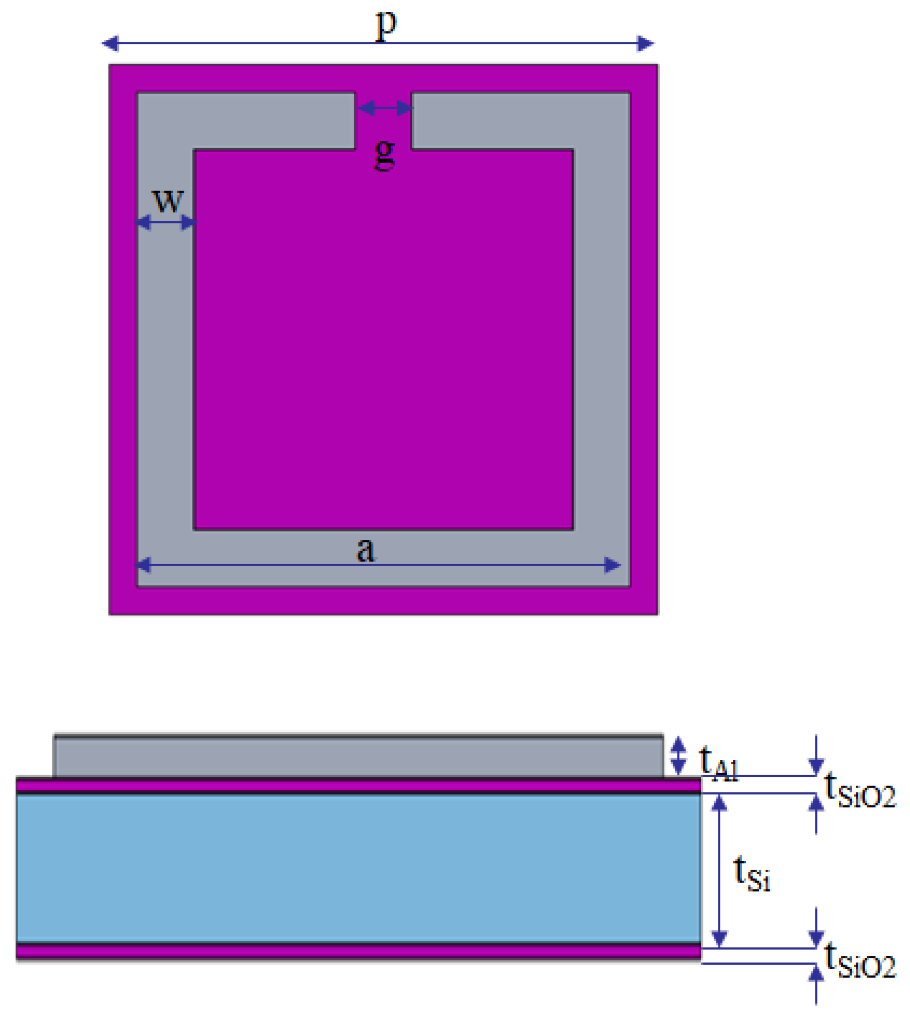
Table 1 and the geometry of the squared SRR structural element with the description of dimensions is shown in
Figure 2. The structure was developed on a 520 µm thick silicon (Si) wafer. First, the wafer was covered with a thermal oxide layer (SiO
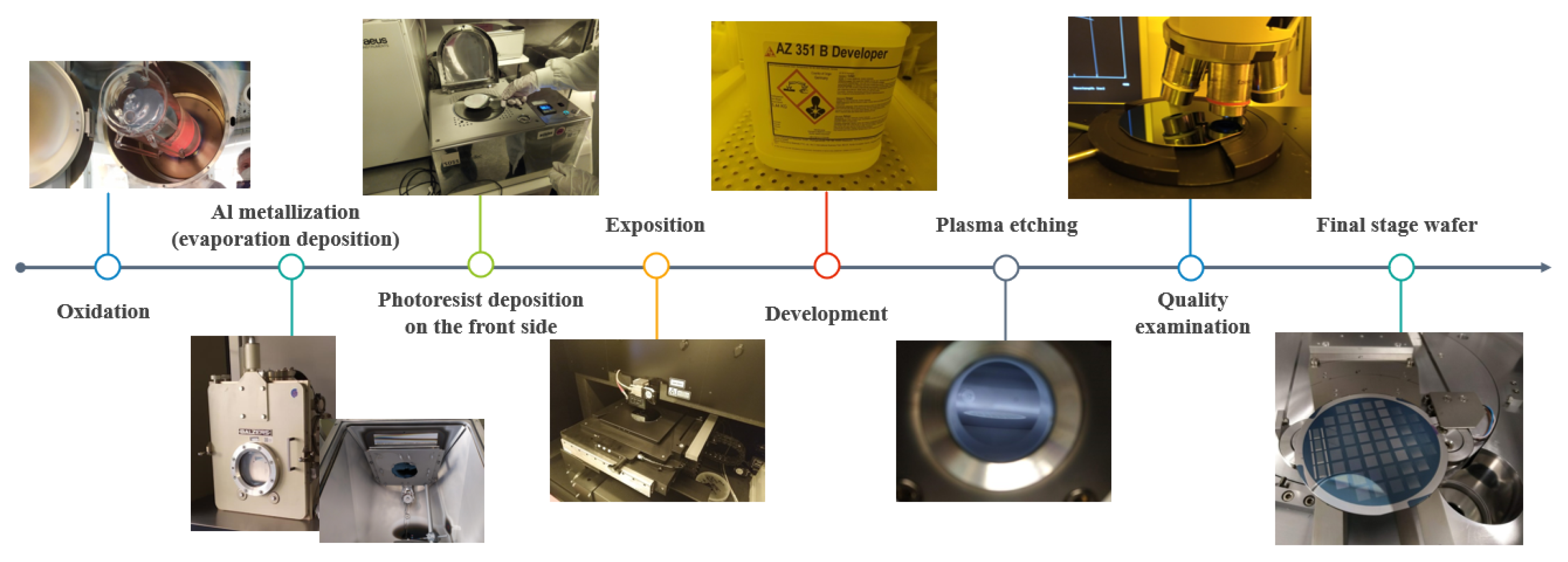
2) (on both sides) with a thickness of 170 nm. The front side of the wafer was coated with thermally evaporated aluminum. The wafer was coated with an AZ 1518 photoresist layer and exposed with the designed terahertz filter mask. The aluminum layer was wet-chemically structured with a phosphoric acid etching mixture, and the photoresist layer was removed in an oxygen plasma. The individual chips for the measurement were separated with a diamond saw. The flowchart of the manufacturing process is shown in
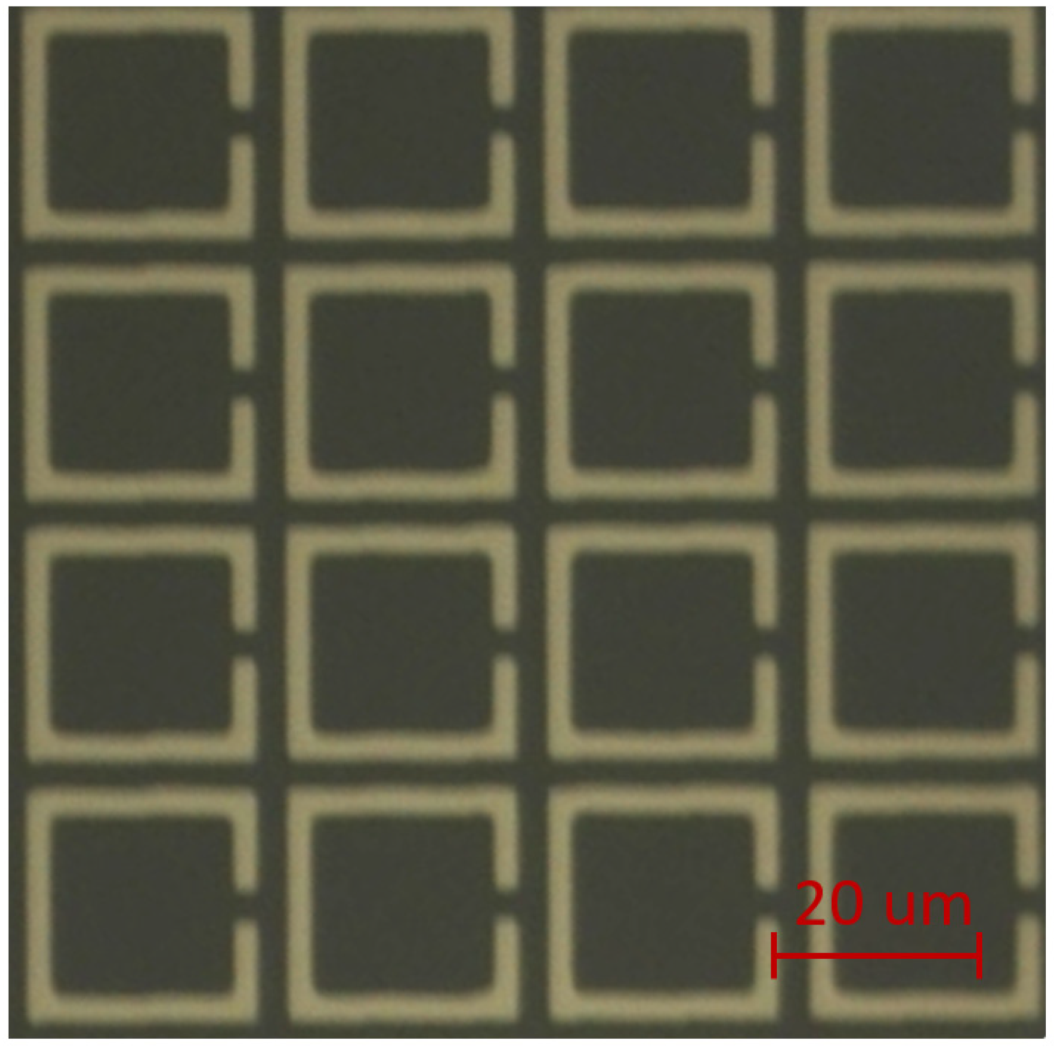
Figure 3. The obtained line width was 2.5 µm, while the capacitive gap was 2.5 µm and the length of the side of the square loop was 21.7 µm.
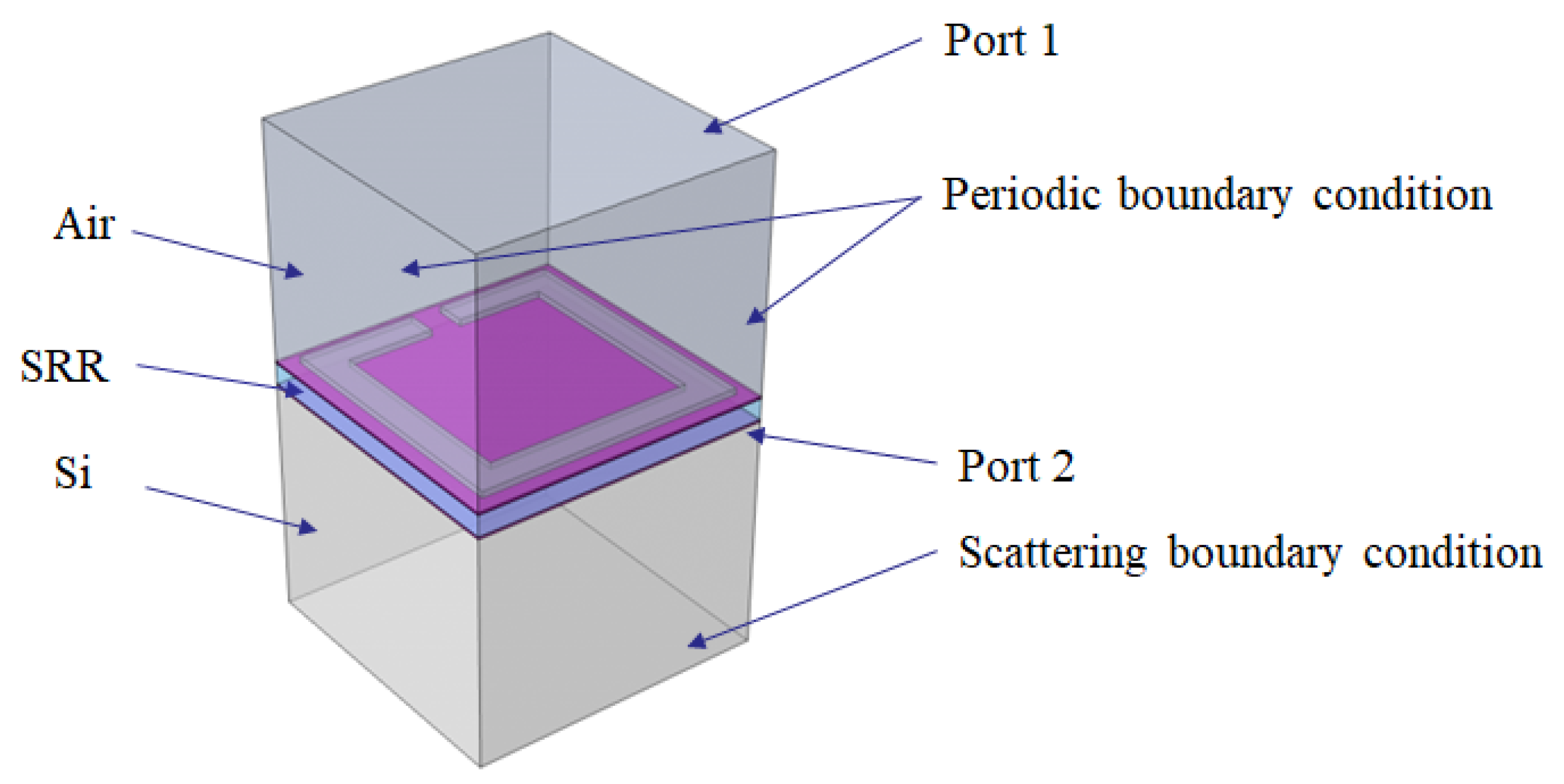
The design and further analyses were carried out using a finite element method (FEM) based numerical model. All the computations were made in the COMSOL Multiphysics 6.0 software. The geometry of the model is shown in
Figure 4. The following values of dielectric properties were assumed for the materials. The refractive index of silicon is
nSi = 3.48 (permittivity is
εrSi = 12.11) [
24]. The real and imaginary parts of the complex permittivity of silicon dioxide for the terahertz range are
ε′
rSiO2 = 4.45 and
ε″
rSiO2 = 0.03, respectively [
25]. The Drude model was used to describe the value of the aluminum refractive index
nAl [
26]:
where
ωp is the plasma frequency of the conductor (depending on the dielectric constant in vacuum, the density of free electrons, electron mass, and charge),
ω is the angular frequency of the incidence wave, and
γ is the damping coefficient of the conductor. The plasma frequency for aluminum is
ωp = 2.123 × 10
16 rad/s, while the damping coefficient is
γ = 1.975 × 10
11/s.
The wave excitation and scattering matrix parameters calculation were enabled through ports (excitation and
S11 calculation on port 1,
S21 calculation on port 1 and 2). Port 1 is placed at some distance over the MS element separated by an air layer, while port 2 is placed on the end of the metasurface stack. The scattering boundary condition was set on the bottom boundary of the computational model in order to fully absorb the outgoing wave and omit its influence on the results including the Fabry–Perot effect. However, this effect can also occur in the case of the Si substrate. For this reason, the solution proposed in paper [
27] was utilized: the Si wafer consisting of metasurface (not in scale in
Figure 4) was backed with an Si layer (not an air layer such as in ordinary operating conditions), and the receiving port was placed on the back surface of the Si wafer. This causes a lack of reflection on the Si wafer‘s back layer boundary. Thus, this configuration makes it possible to eliminate the Fabry–Perot effect while conserving the original response of the metasurface. The Fabry–Perot effect strongly affects the results obtained in the terahertz frequency range (multiple, relatively high amplitude ripples obtained in spectrum); thus, in the case of frequency domain computations, some sophisticated methods for its reduction should be applied.
In this high-frequency electromagnetic problem the following frequency domain equation is solved [
28,
29]:
where:
E—electric field,
µr—relative permeability,
ε0—permittivity of vacuum,
εr—relative permittivity,
σe—electric conductivity,
k0—wave number,
ω—angular frequency. The exemplary mesh used during numerical calculations consists of 106,029 domain elements, 17,278 boundary elements, and 1602 edge elements.
To reduce the computational complexity of the developed model (instead of the simulation of a large matrix of structural elements) just a single-element analysis was performed. This simplification was based on the application of Floquet periodic boundary conditions on the side boundaries. Such simplification of the model is acceptable, as will be shown later in this paper, through the comparison of modeled and measured resonant frequencies and S21 reflection coefficient frequency responses.
To investigate the influence of the fabrication process and material properties on the quality of the designed SRR structure, the following parameters were analyzed: etching deviation
e, metallization thickness
tAl, and SiO
2 layer thickness
tSiO2. The quality of the metasurface affected by the above parameters was determined by the deviation of resonant frequency Δ
fr:
where
frD—resonant frequency of the structure with deviated parameters,
frB—resonant frequency of the structure with a base set of parameters (shown in
Table 1).
The influence of each of the above parameters on the behavior of the metasurface was determined using a developed finite element method (FEM)-based numerical model.
3. Results
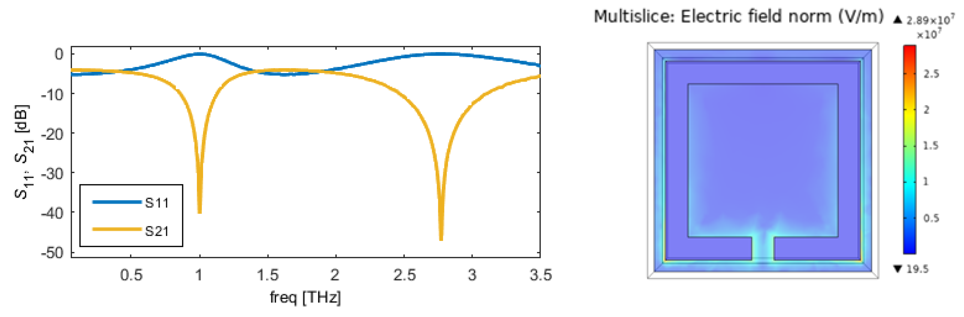
The developed numerical model was utilized to perform the considered analyses. The exemplary results of the simulations are presented in
Figure 5; the frequency response of transmission |
S21| and the reflection |
S11| scattering matrix parameters were presented for the dimensions given in
Table 1. One can observe that there are two resonances: 1 THz and 2.77 THz. The distribution of the electric field on the surface of MS is shown for the first resonance (frequency of 1 THz). As was expected, there is an enhancement of the electric field intensity in the vicinity of the capacitive gap. The presented results show that the designed metasurface meets the requirements assumed in the design process. This positive verification allowed us to perform the fabrication process based on the dimensions presented in
Table 1. The photo of the fabricated structure is shown in
Figure 6.
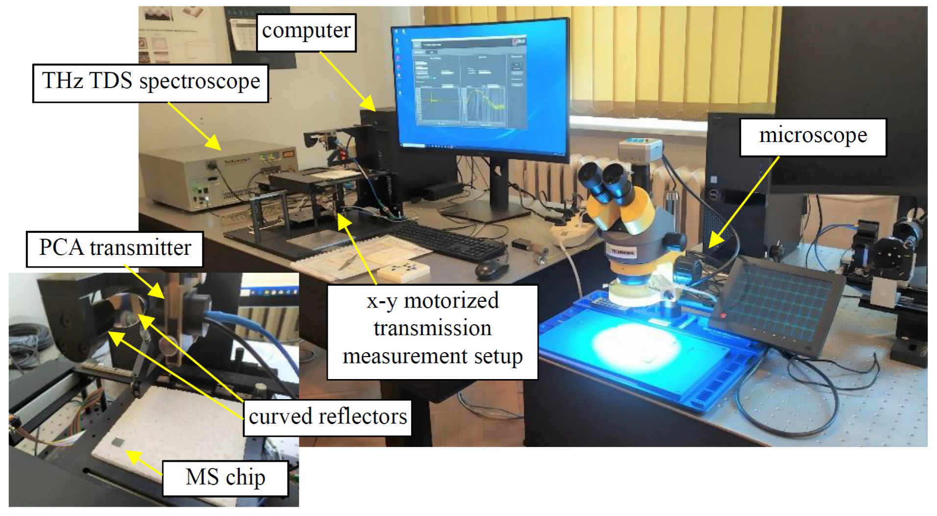
The fabricated structure was experimentally evaluated to verify the results of the design process, as well as the numerical model and the applied assumptions (such as frequency domain computation, Floquet periodic boundary conditions, plane wave excitation, dispersive modeling of the metallization layer, etc.). The measurements were performed using the THz-TDS (terahertz time domain spectroscopy) system TeraFlash smart of Toptica, Germany, shown in
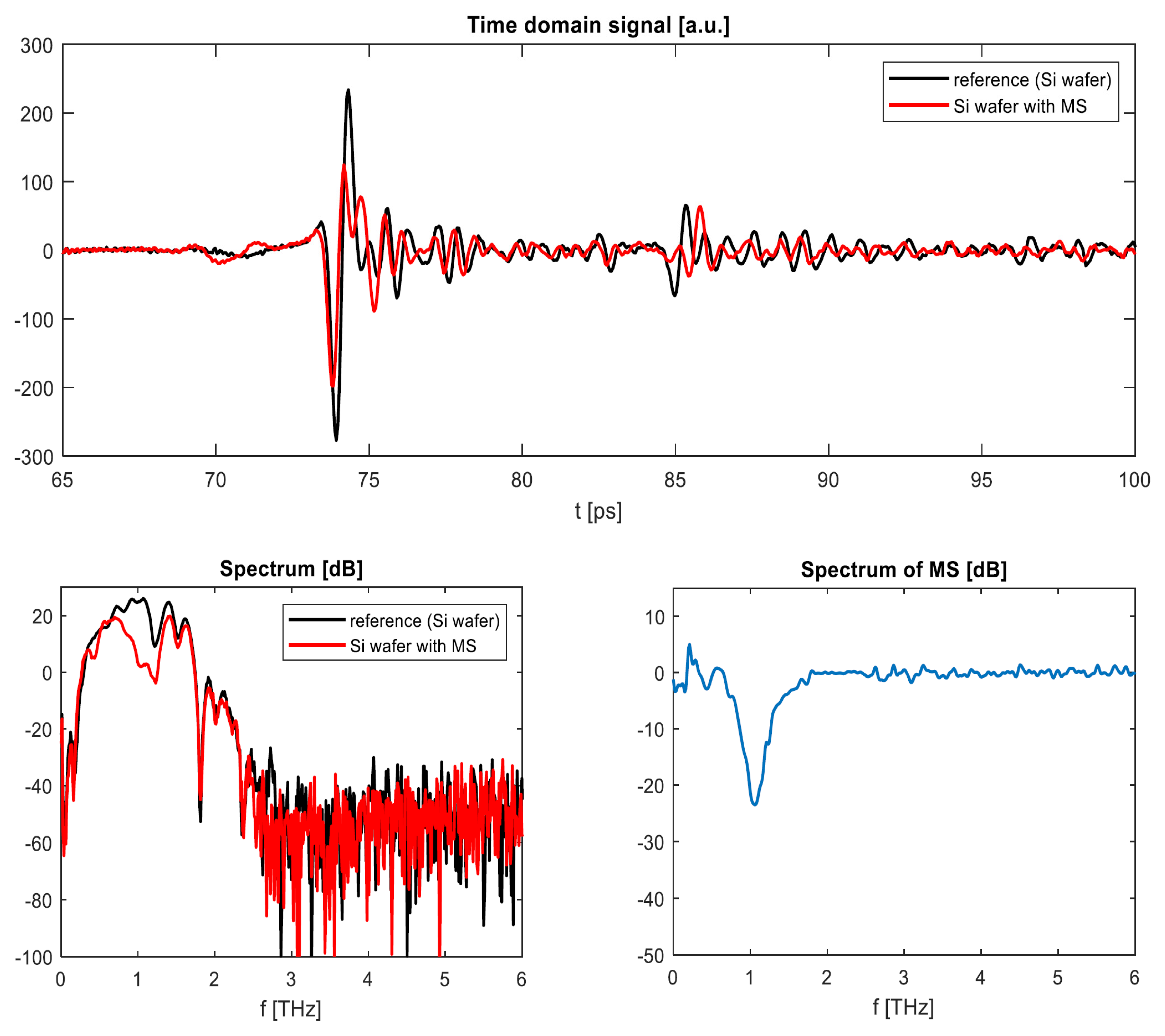
Figure 7. A transmission setup was utilized, whereby the transmission Tx and receiver Rx heads are on opposite sides of the examined device/structure under test (DUT). The electromagnetic pulse with a terahertz frequency content is generated by a photoconductive antenna and focused on the evaluated metasurface structure using a set of curved reflectors. After interaction with the DUT, the modified pulse defocuses and propagates through another set of curved reflectors and is passed to the receiving photoconductive antenna. The focusing spot size (the area of incidence of the terahertz beam) is less than 1 mm diameter. The results of the measurements are presented in
Figure 8. The presented time domain pulses were obtained for two scenarios: the Si wafer without metasurface (reference signal), and the Si wafer containing an MS. As the frequency domain data are of more importance in the considered analysis (resonant frequency analysis), a transformation of the data from the time to frequency domain was obtained using Fourier transform. In the first step, the measurement without DUT was made (air transmission spectrum) in order to verify the transmission band. In the obtained frequency response, the usable signal (above the noise level) can be observed for the frequency band below 2.5 THz. This means that the second resonance will not be possible to measure for this configuration (the frequency responses presented in
Figure 8 obtained for the Si wafer also confirm a maximum usable frequency of 2.5 THz). Within the transmission band, there are multiple absorption peaks visible, caused by the absorption of certain frequencies by water, nitrogen, and oxygen molecules. In the next step, the measurement of the Si wafer without metallization was made to obtain the reference signal. Finally, the measurement of full DUT (the Si wafer with a metallization metasurface) was performed. One can observe the decrease in the transmission spectrum in the vicinity of a frequency of 1 THz, which is caused by the resonant behavior of MS. After de-embedding, the metasurface transmission spectrum consists of just one (primary) resonance for the desired frequency of 1 THz. The resonant frequency obtained in the simulations was
fr1Sim = 1.0023 THz, and in the measurements was
fr1Meas = 1.040 THz. Good agreement between the simulations and measurement results was proved by an absolute difference of 37.7 GHz and a relative difference of 3.76%. The measurement results are consistent with the resonance frequency
fr = 1 THz assumed in the design process and is within the deviation of +46.47 GHz/−42.83 GHz determined (in a later part of this work) by numerical analysis. As indicated in the article, due to the limited bandwidth of the measurement system used, experimental verification in the case of the second resonance was not possible.
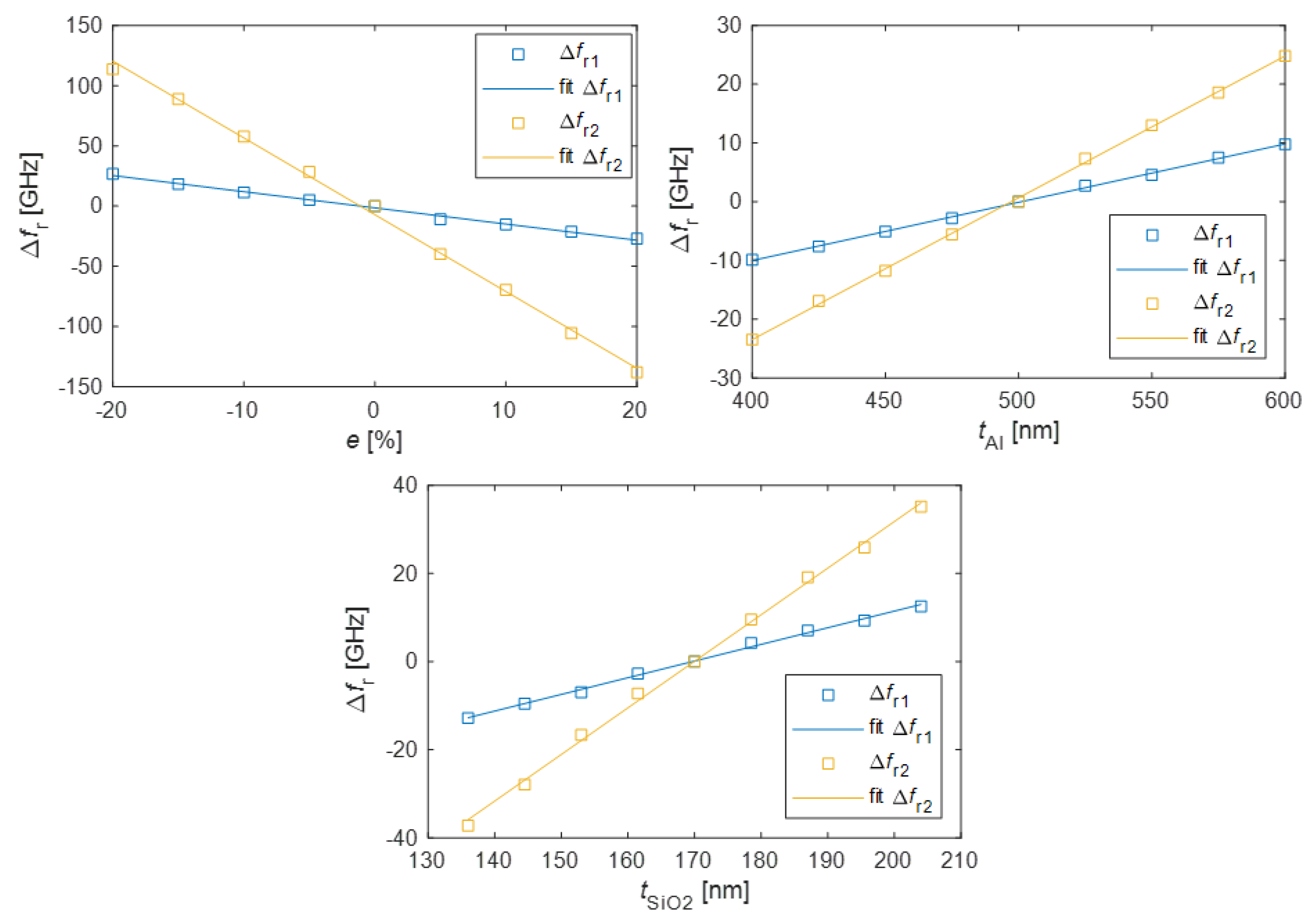
After positive verification of the developed numerical model and all the assumptions made, analysis of the influence of selected geometrical parameters was performed. These parameters (etching deviation
e, metallization thickness
tAl, and SiO
2 layer thickness
tSiO2) were selected as the most susceptible to possible deviations during the production process. The values of the
tAl and
tSiO2 parameters presented in
Table 1 were taken as reference values, and during the analysis, these values were changed in the range of ±20% of the reference value:
e = −20… + 20%,
tAl = 0.400…0.600 µm and
tSiO2 = 0.136…0.204 µm. The etching deviation parameter is a more complicated value, consisting of the line width
w, which was changed from the range of ±20%, while simultaneously changing the gap
g and the square loop size
a. The considered values of
w,
g, and
a for the different values of the etching deviation parameter
e are shown in
Table 2.
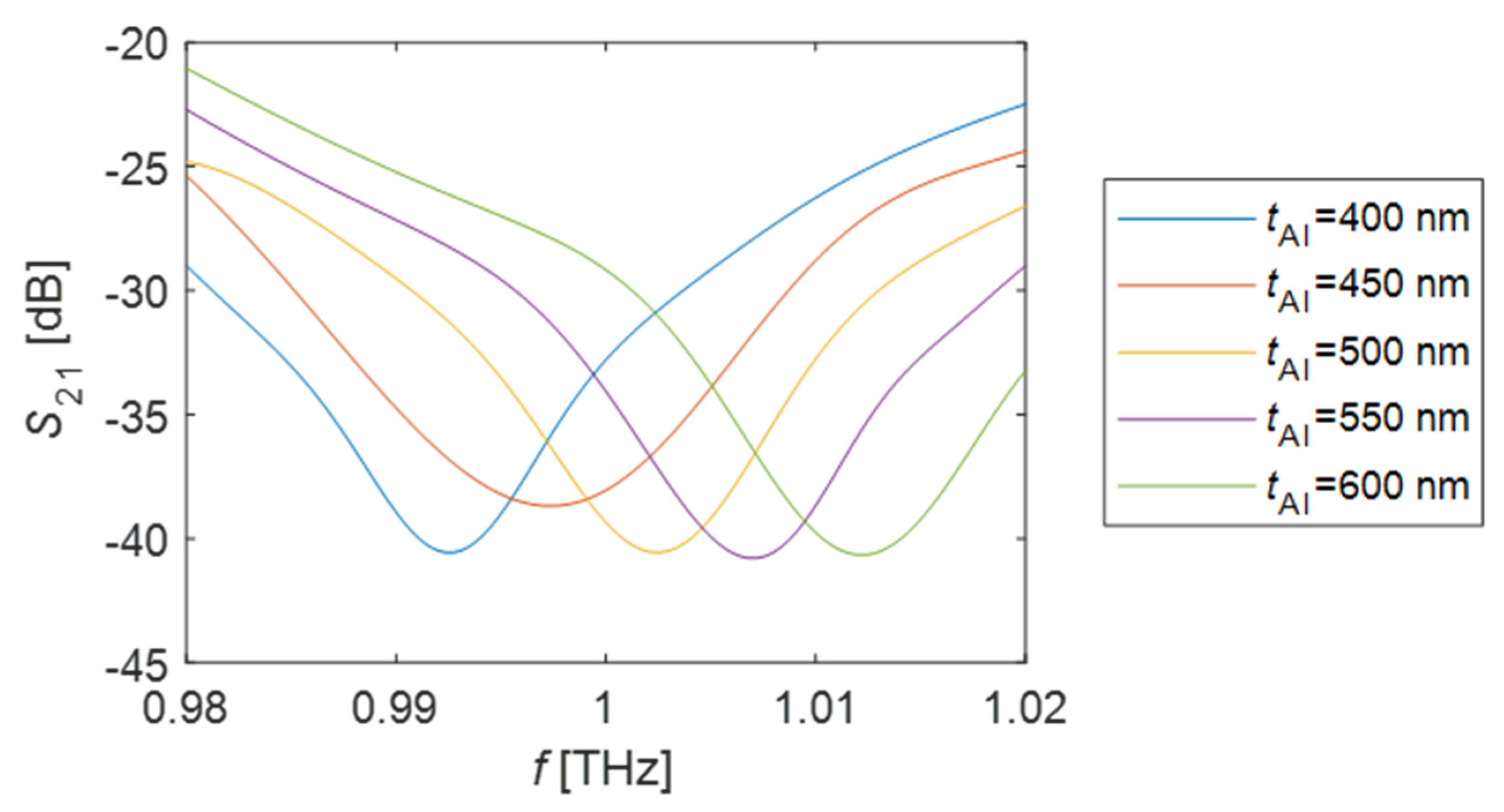
An exemplary result of such analysis—the shift of the resonant curve caused only by the change in the metallization layer thickness
tAl—is presented in
Figure 9. One can observe the increase in resonant frequency
fr1 while the metallization thickness
tAl increases. This relationship is presented for both resonances and all three considered parameters in
Figure 10. In all cases we can observe a quasi-linear relationship when considering ±20% variation ranges.
The influence of the analyzed parameters can be considered based on an equivalent circuit—for SRR—schematically modeled as a parallel resonant circuit with a resonance frequency
frSCH [
30]:
where
frSCH—resonant frequency of equivalent circuit,
L—equivalent inductance,
C—equivalent capacitance.
Increasing the thickness of the metallization increases the conductance but decreases the inductance of the wire constituting the resonant ring. Reducing the inductance in the equivalent circuit increases the resonant frequency.
The capacitance of the SRR structure depends to the greatest extent on the capacitance of the gap, which can be approximated by a flat capacitor, in which the electric field is partially distributed in air and partially in a silicon wafer, in particular the SiO2 layer on the surface. Therefore, to determine the capacitance, it is necessary to use the equivalent permittivity (depending on the depth of the SiO2 layer). In the case of a thin SiO2 layer, part of the electric field exists in the Si (high permeability) layer. The increase in the thickness of the SiO2 layer causes the electric field to be distributed to a greater extent in the material characterized by lower permittivity, so as a consequence the resultant capacitance decreases. A smaller value of the gap capacitance increases the resonant frequency.
According to
Table 2, an increase in the etching deviation factor causes an increase in linewidth and square loop size and a decrease in capacitive gap size. An increasing linewidth causes a decrease in the inductance and, as a result, an increase in resonant frequency. A reduction in gap size causes a higher capacitance and consequently a lower resonant frequency. If the square loop size increases, the inductance increases too, thus the resonant frequency decreases. Finally, in the case of the etching deviation factor increasing, the resulting resonance moves to lower values.
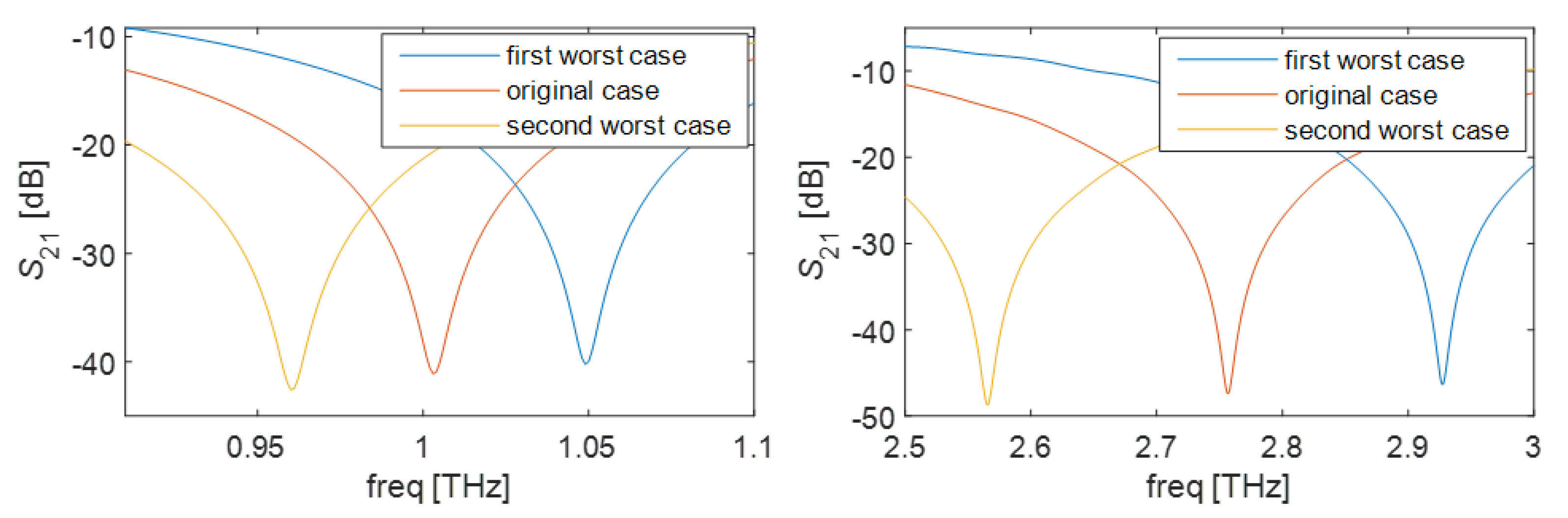
The comparison of the influence of considered parameters on the maximum shift of resulting resonant frequencies is presented in
Table 3. The comparison was divided into two stages: first, each of the considered parameters was analyzed separately, then two worst-case scenarios were verified:
first worst case: the lowest considered etching deviation e, and the highest considered metallization layer thickness tAl, and silicon dioxide thickness tSiO2—causing an increase in resonant frequencies;
second worst case: the highest considered etching deviation e, and the lowest considered metallization layer thickness tAl and silicon dioxide thickness tSiO2—causing a decrease in resonant frequencies;
This was possible because of similar and monotonic characteristics of the relationships shown in
Figure 10.
In the case of only one parameter variation, the biggest influence was caused by the line etching deviation
e, while the smallest one was by aluminum thickness
tAl. The frequency shifts, as expected, were 2–5 times higher for the second resonance. Finally, in the case of the worst-case scenario (all the considered parameters deviations were taken into account), the maximum change in
fr1 was close to 46 GHz and the change in
fr2 was 192 GHz. This caused the following relative deviations of resonant frequencies: 4.6% for
fr1 and 6.9% for
fr2. The shifts of resonant curves caused by the cumulative change in etching deviation
e, aluminum layer thickness
tAl, and silicon dioxide thickness
tSiO2 are presented in
Figure 11.
4. Conclusions
In this paper, the design and fabrication of split-ring-resonator-based metasurfaces were performed and a further analysis of the fabrication process uncertainty on resulting MS parameters was numerically conducted. The process of terahertz metasurface fabrication is relatively complicated (lots of parameters need to be precisely controlled), and may be the source of some deviations from the planned (designed) dimensions resulting in shifts of assumed electromagnetic parameters. The sources of probable inaccuracies in the fabrication process were identified (etching process deviation e, aluminum metallization thickness tAl, and silicon dioxide layer thickness tSiO2 variations) and their influence was analyzed using the numerical model. The commonly utilized metasurface structure of the square split-ring resonator was chosen and designed for operation in the terahertz frequency range. In this case, not the full matrix of structural elements but a single-element numerical analysis (with periodic boundary conditions) was utilized. This assumption regarding the periodicity enables the examination of various fabrication aspects, as long as there is no asymmetry in the metasurface’s geometry.
It was assumed that the geometrical parameters (e, tAl, and tSiO2) were modified in the range of ±20%. All the evaluated sources of geometric deviation caused a linear change in both resonant frequencies. This caused the following relative deviations of resonant frequencies: 4.6% for fr1 and 6.9% for fr2. Such frequency deviations can cause significant degradation of the MS performance in some applications. Depending on the application of a particular metasurface, other parameters (than resonant frequency) should be considered for evaluation; e.g., in the case of reconfigurable structures (flexible or MEMS devices), tunability range can be evaluated.


 ,
, 


