1. Introduction
Space-fed electronically reconfigurable transmitarray antennas (SERTA) are in great demand due to their distinct features, such as a high gain, a low profile, a low cost, built structures, and feed options. These SERTA pictorial characteristics have attracted many researchers in the last few decades due to their wide applications in beam-forming and beam-scanning areas [
1,
2,
3,
4,
5]. It includes satellite communication (SATCOM), civil and military radar systems, and 5G/6G communication systems for mobile access points [
6]. Phase array architectures are typically heavy and bulky, making them unsuitable for various applications. Researchers have recently focused more on low-profile and compact designs. Much work has been conducted to achieve these characteristics in space-fed electronically reconfigurable transmitarray antennas for feed optimization and a compressed focal distance [
7]. Most of the space-fed transmitarrays are not reconfigurable [
8,
9,
10]. Reconfigurable technology is realized with the mechanical spinning of the systems, e.g., a motor. This method is still used nowadays due to its cost-effective waterproof behavior and ease of fabrication.
On the other hand, this approach is unsuitable due to the bulky system design, mechanical vibrations, and higher latencies. The development of electronic components and miniaturization at higher frequency bands open new ways for the researcher to implement and design electronically reconfigurable beam-scanning and beam-forming arrays. These components are also helpful for implementing the transmitter (Tx)/receiver (Rx) modules.
There are several reconfigurable components available to acquire beam-scanning and beam-forming operations, such as PIN diodes [
11,
12,
13,
14,
15], varactor diodes [
16], RF-electromechanical systems [
17], liquid crystal and micro-fluids, etc. Each component has its pros and cons according to application requirements. There are multiple techniques reported in the literature, such as the multilayer frequency selective surface (MSFF) [
18], material transformation approach [
19,
20,
21], and transmitter–receiver method [
22,
23], to design a transmitarray. The global demands for high data rates are rising day by day, and several applications of communication systems are driving researchers toward seeking a solution to address the high demand for data rates and higher bandwidth. Some efforts are utilized to design the high-bandwidth reconfigurable transmitarrays in the literature. A one-bit reconfigurable transmitarray is reported with varactor diodes placed on the microstrip patch antenna having 1 GHz bandwidth attained in a unit cell. Still, insertion losses are high due to the high insertion losses of varactor diodes [
24]. A rectangle O-shaped slot transmitarray unit cell was designed with two diodes; however, the bandwidth of the unit cell was obtained at 14.1% [
25]. A design with wide beam scanning and high bandwidth was presented with a high profile and a complex structure. In another work, a linearly polarized transmitarray for the Ku band was proposed using two orthogonal H-shape slots. The presented design has a 3 dB measured gain bandwidth of 9.6% [
26].
This paper proposes a low profile and wideband electronically reconfigurable transmitarray at Ku band, essential in detecting drone strike technology (KuRFS) and radar and satellite communications. The bandwidth of most electronically reconfigurable transmitarrays (ERTA) is insufficient compared to the previously used phased arrays. Some of the disadvantages of ERTA in the literature include a significant gain scan loss and narrow bandwidth. Therefore, enhancing the ERTA’s beam-scanning capability is essential to decrease the gain scan loss and increase the bandwidth. This research proposes a wideband meander-lines, one-bit electronically reconfigurable transmitarray at Ku band with linear polarization. The proposed unit cell works on polarization selection, and the polarization rotation is based on the symmetric current reversal phenomenon. It uses a hexagonal patch with an offset feed to realize a transmitarray unit cell design and a transition waveguide. Full-wave simulations have been carried out in the ANSYS HFSS and CST microwave studio to analyze and observe the behavior of the transmitarray unit cell. A reconfigurable transmitarray with 20 × 20 antenna elements has been realized. A full-wave simulation of 400 elements has been performed to observe the E- and H-plane scanning capability of the transmitarray, along with the directivity, gain, side-lobe level (SLL), and aperture efficiency.
This paper is organized as follows: The design and optimization of the transmitarray unit cell and the operating principle of the unit cell are described in
Section 2. The numerical scattering parameters of the proposed unit cell and the effects of the bias circuit are demonstrated in
Section 3. The measured results of the unit cell in the waveguide environment are described in
Section 4. The design and full-wave simulations of the 20 × 20 transmitarray are illustrated in
Section 5. Finally, this paper is concluded in
Section 6.
2. Design and Optimization of Proposed Unit Cell
The transmitarray is a type of electromagnetic surface antenna that is either a two-dimensional periodic or quasi-periodic artificial electromagnetic structure. A reconfigurable electromagnetic surface was designed by introducing tunable electric devices on the electromagnetic surface unit cell. The EM waves can be controlled in real time through tunable electronic devices for beam agility/scan purposes. In this section, we design a one-bit electronically reconfigurable controlled electromagnetic surface unit and array; the core issue is how to make ordinary transmitarray unit cells have 0°/180° numerically controlled phase shift capability. Therefore, an excellent one-bit phase-shift structure should meet the following characteristics: ideal 180° phase difference in the two-phase states, simple structure, and compact integration with the transmitter and receiver structure. Based on the above considerations, a commonly used design method for the transmitarray unit cell is the phase-shifting structure of the transmitter. In this type of unit cell design, the reconfigurable device is usually integrated into the design of the receiving patch antenna or the transmitting patch antenna to change the quantization state. The phase of the EM wave is changed through the electronic device that controls/changes the path of the resonant patch antenna.
Design of Proposed Unit Cell Structure
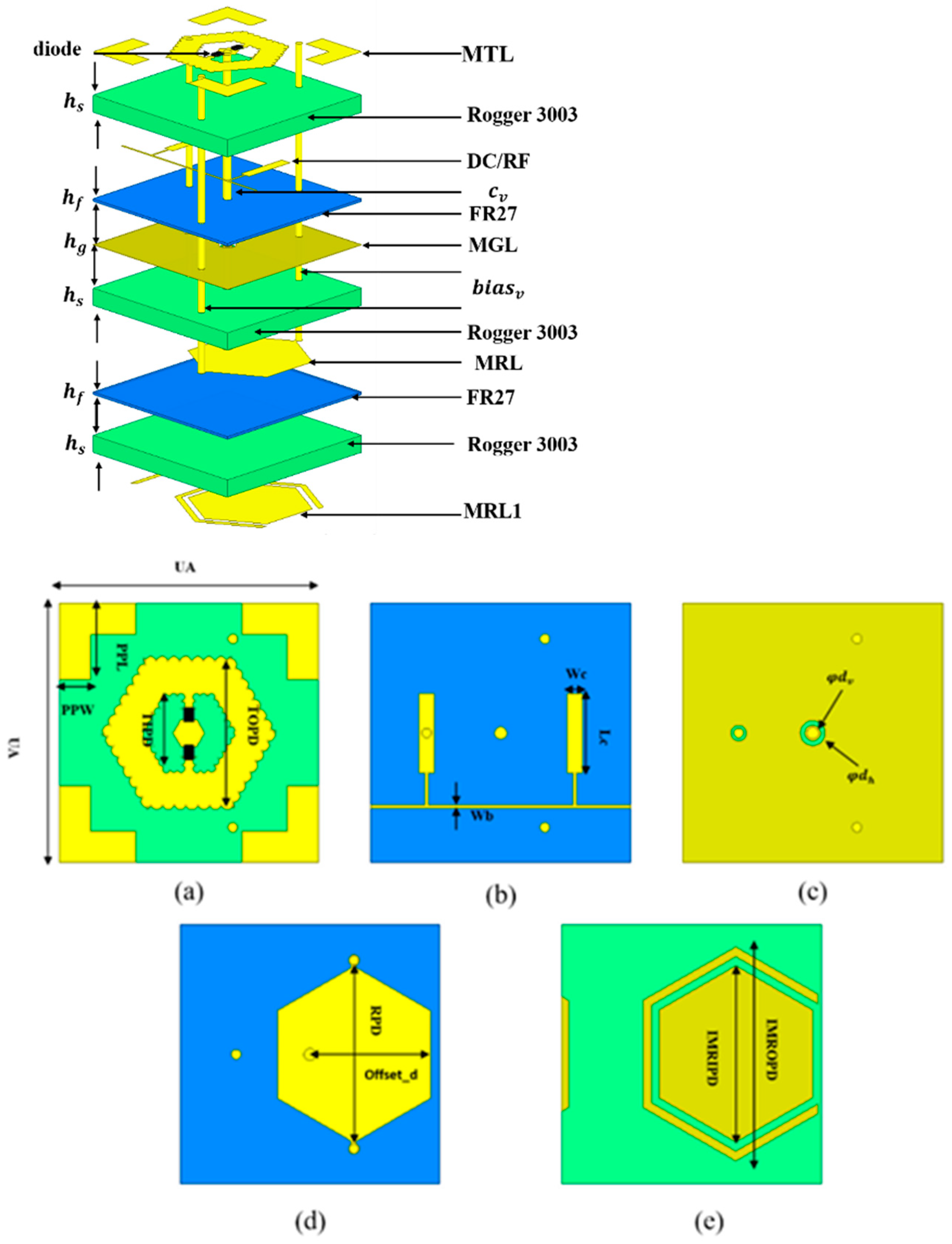
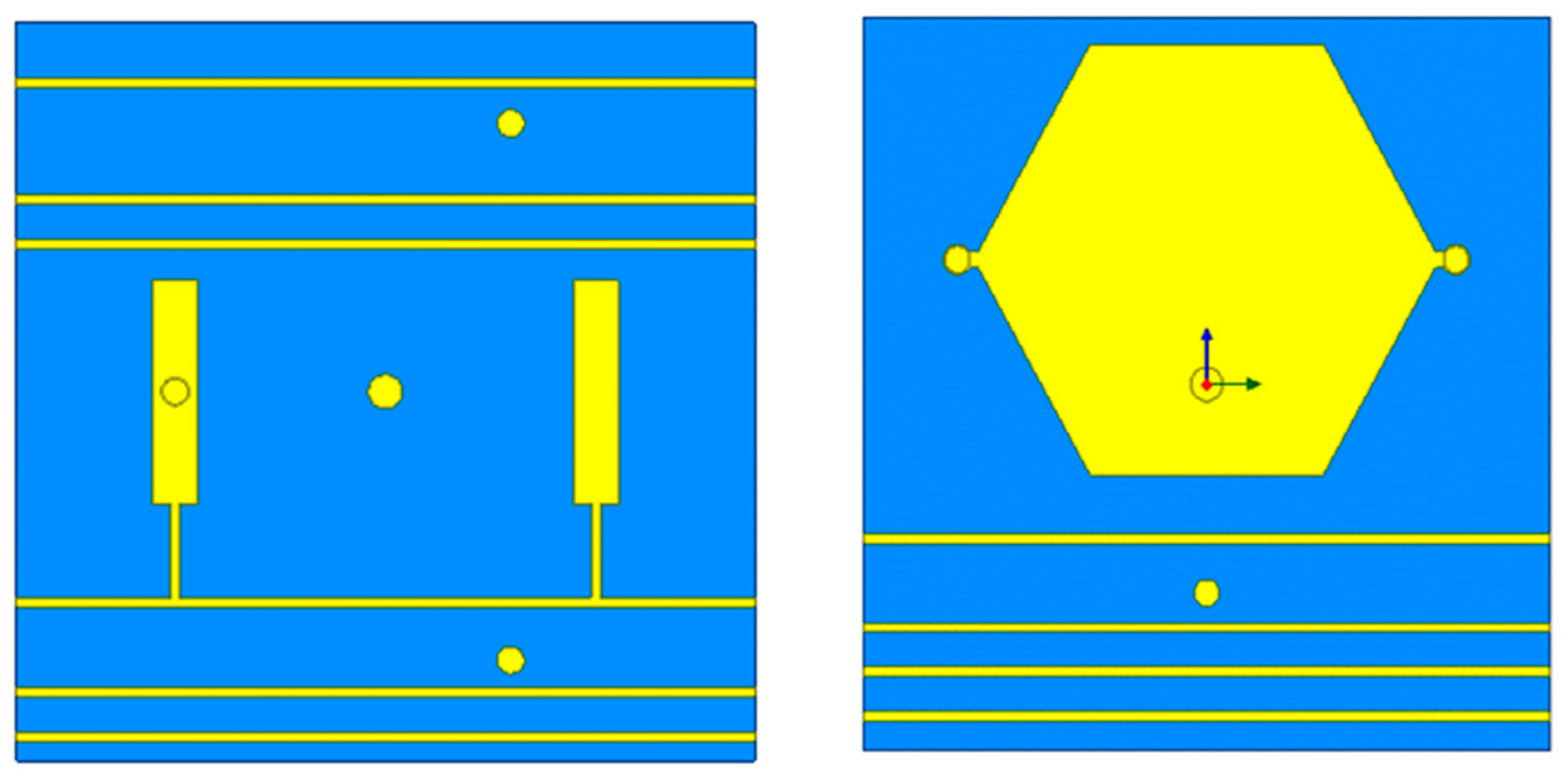
A hexagonal meander-shaped broadband reconfigurable transmitarray unit cell structure design is proposed, and its basic unit structure is shown in
Figure 1. The dimensions of the offered unit cell are
(0.45λ
0 × 0.45λ
0 × 0.13λ
0) at 16.5 GHz, where λ
0 is the free space wavelength. The architecture of the unit cell is composed of five metal patches etched on three similar substrates. The receiver and transmitter metal layers are named MTL and MRL1, as shown in
Figure 1a,d. The hexagonal patch is used with O-slot to integrate the PIN diode to achieve phase resolution for the transmitter (Tx). Two hexagonal patches have been used for the receiver (Rx), one for receiving the electromagnetic waves and the other to enhance the receiver’s impedance matching. The receiver (Rx) MRL1 layer and transmitter (Tx) MTL are joined with a 0.3 mm metallic interface integrated at the center of the unit cell and separated by a ground layer (MGL). There are two bonding films used to join the substrates. Transmitter layer MTL, receiver layers MRL1 and MRL2 are etched on Roger RO6002 (ε
r = 2.94, tanδ = 0.0012) with a thickness of 0.78 mm. A total of 2 bonding films FR 27 (ε
r = 2.94, tanδ = 0.001) join 3 Roger RO6002 substrate layers. However, the thickness of each bonding film is 0.1 mm. All the dimensions are tabulated in
Table 1.
The top view of the transmitting layer (T
x), as demonstrated in
Figure 1a, is used to transmit radiating electromagnetic waves into the free space. The O-slot on the transmitter layer divides the patch into internal and external hexagonal patches, which integrate with the two anti-parallel diodes. Two PIN diodes are mounted in the same direction along the
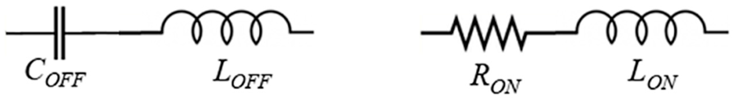
x-axis to transmit electromagnetic waves with horizontal polarization. A one-bit phase resolution was obtained using two PIN diodes added to an active unit cell. The bias lines used on the transmitter and the bonding film to control the positive polarity of the diode. At the same time, negative polarity is accomplished with the ground. The serial number of the PIN diodes used in the design is (MADP-000907-14020). The diode requires +1.3 V for forward bias and −1.3 V for reverse biasing. The value of series resistance R = 7.8 Ω with inductor value L = 30 pH for on state, whereas the values of capacitance are C = 25 fF and L = 30 pH in series for off state.
The PIN diodes integrated into the active elements are always biased in the opposite direction. One diode operates in the ON state while the other works in the OFF state. This design ensures the 2 diodes remain on and off all the time, permitting a 180-degree phase difference by reversing the current on the structure. These switching states produce two states directed to the opposite surface current, generating 0° and 180° phase shifts. The bias lines are etched on bonding film as illustrated in
Figure 1b and are used to operate the PIN diodes. The DC bias network consists of two capacitive plates to separate RF signals from biasing voltages of diodes.
The design principle of the unit cell is incorporated to achieve wideband resonance characteristics and one-bit phase shift control characteristic. The proposed unit cell utilizes a meander shape, re-resonating parasitic patches, and dual hexagonal impedance-matching patches. The hexagonal structures resonate on higher resonance modes with primary as circular mode. Higher resonance modes can be tuned with the lower resonance mode to enhance the bandwidth of the acquire layer. The transmitter-layer hexagonal patch is engraved with meander shapes to improve the structure’s bandwidth capability. These are designed based on the linear equation d1 = k × d2, where d2 is the diameter of the outer-ring meanders of the hexagonal angular patch and d1 is the diameter of an inner-ring meander of the hexagonal angular patch of the transmitter layer. is the meander constant, which can vary from 0.2 mm to 0.9 mm, whereas is used in this structure as the optimization meander constant value of the structure.
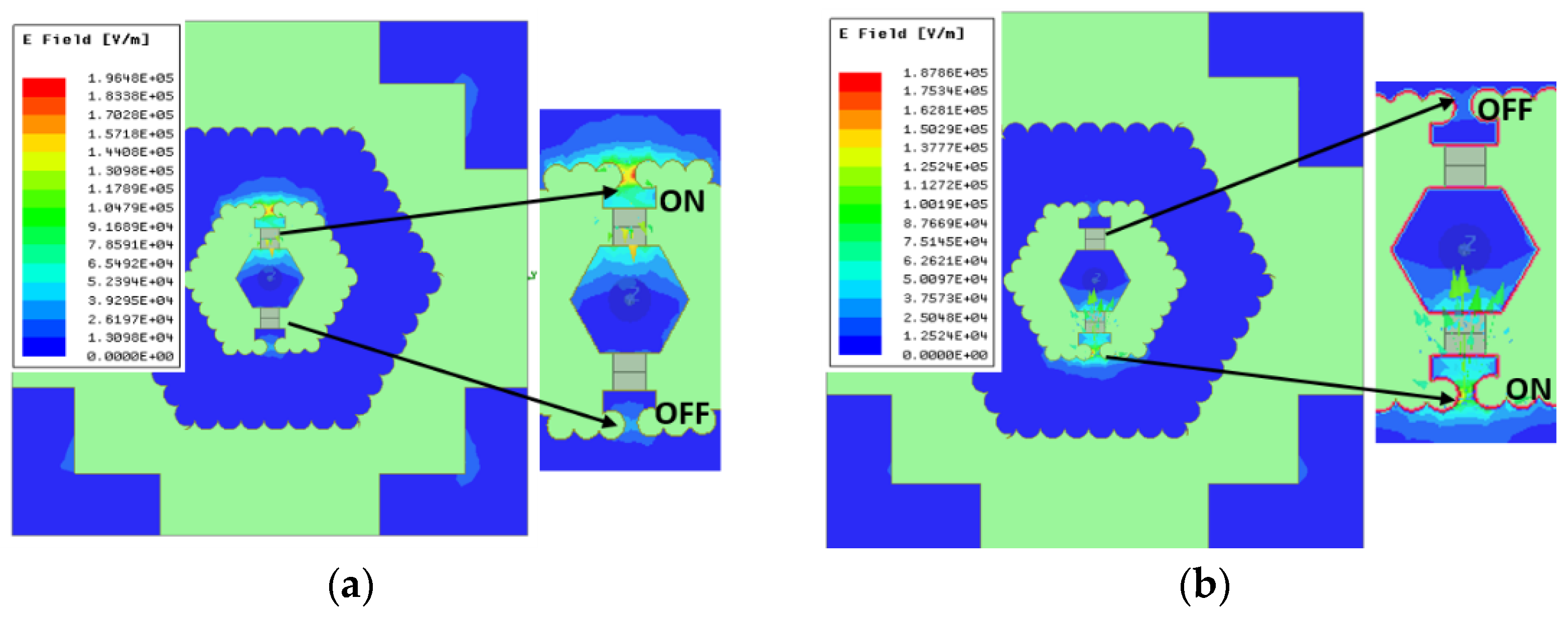
The 4-edge parasitic patches are used to re-resonate the resonating antenna’s EM field to enhance the desired range of frequencies of more than 500 MHz. The E-field of the resonating patch at 16.5 GHz is demonstrated in
Figure 2 to understate the phase state control operation of the proposed unit cell. The propagation pathway of state I and state II are reversed. The phase shift control of the unit cell is attained by changing the propagation path in the mirror direction under the current path reverse direction phenomenon. The radiation layer of the transmission array element adopts the cascade structure design. The lowermost receiver and impedance-matching layer both form a cascade from the receiver layer of the unit cell to realize EM waves from the feed source. The structure expands the bandwidth and can be used as a wide-angle impedance-matching layer to improve the beam-scanning characteristics of the transmitarray. The layer’s offset distance relative to the substrate’s center (along the
y-axis) is d, and the y-polarization mode radiates the electromagnetic wave.
3. Scattering Parameters
The proposed unit cell design has been simulated and analyzed in commercial electromagnetic high-frequency simulation tool ANSYS HFSS and CST Studio Suite 3D EM simulation and analysis software with master–slave periodic conditions, and the unit cell is excited with Floquet port excitation. We use periodic boundary conditions to analyze the transmitarray unit cell scattering parameters and other characteristics. The side walls of the unit cell are realized in master–slave boundary conditions. Floquet-Port 1 (FP1) and Floquet-Port 2 (FP2) are added to the upper and lower boundaries of the air box, and the TE and TM modes of the Floquet port are utilized to simulate X-polarization and Y-polarization of the incident electromagnetic waves, respectively. The transmitarray unit cell characteristics and its polarization modulation function can be accomplished by setting the master–slave boundary conditions and adding Floquet ports. The scattering parameters full-wave simulation on normal incident angle present two-phase states scattering parameters as shown in
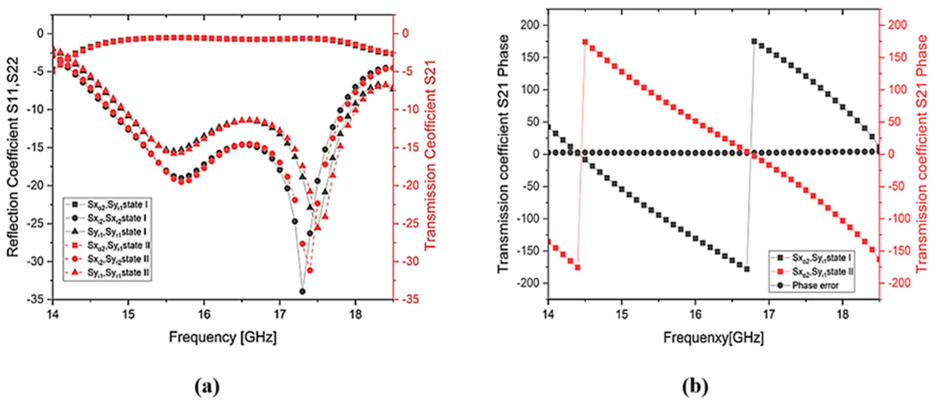
Figure 3a with detailed analysis for incident and radiation angle parameters.
Table 2 is less than −10 dB from 14.94 GHz and from 18.01 GHz for state I and state II due to the current symmetric structure. The passive patch reflection coefficient
has −10 dB bandwidth ranging between 14.77 GHz and 17.86 GHz for both state I and state II with symmetric reflection losses. The minimum insertion loss is only 0.56 dB at 16.5 GHz with a 1 dB transmission bandwidth S
and is between 14.38 GHz and 17.83 GHz for both state I and state II, with symmetric current characteristics. However, the 3 dB transmission bandwidth S
lies from 14.26 GHz to 18.63 GHz with symmetrical current characteristics to maintain maximum useable bandwidth for both state I and state II illustrate in
Figure 4a. The phase difference of 180° is achieved for both states with a maximum error of 3° due to symmetric current distribution over the unit cell, as presented in
Figure 4b. This phase error is reduced to make a theoretically consistent transmission performance, and the passive patch is rotated by 90 degrees against the active patch. In this way, the current distribution of the total element is symmetric at both states; thus, the transmission curve of both states is almost the same.
In the annular gap part of the electromagnetic wave transmitter patch, there is a tunable electronic device (PIN diode) for phase shifting. As a result, to control the switching state of the two diodes on the “regular hexagonal ring” patch, the electric field phase can be reversed by 180°, thus achieving a one-bit phase shift.
Figure 3b shows the phase variation curves of different channels (diode state changes) with frequency in two states of electromagnetic waves. The phase difference between the 2 states is kept at 180°, illustrating the feasibility of a 1-bit proposed design.
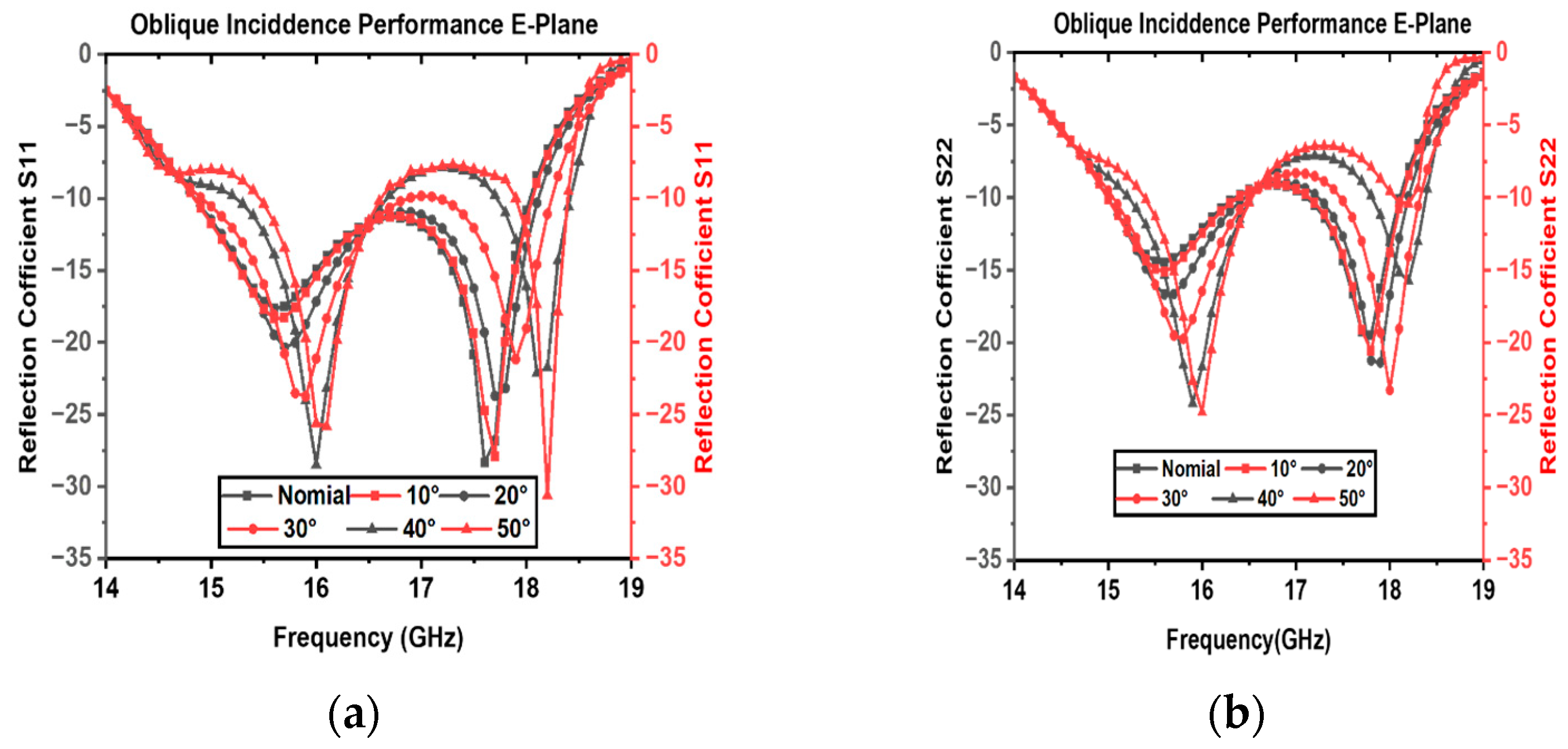
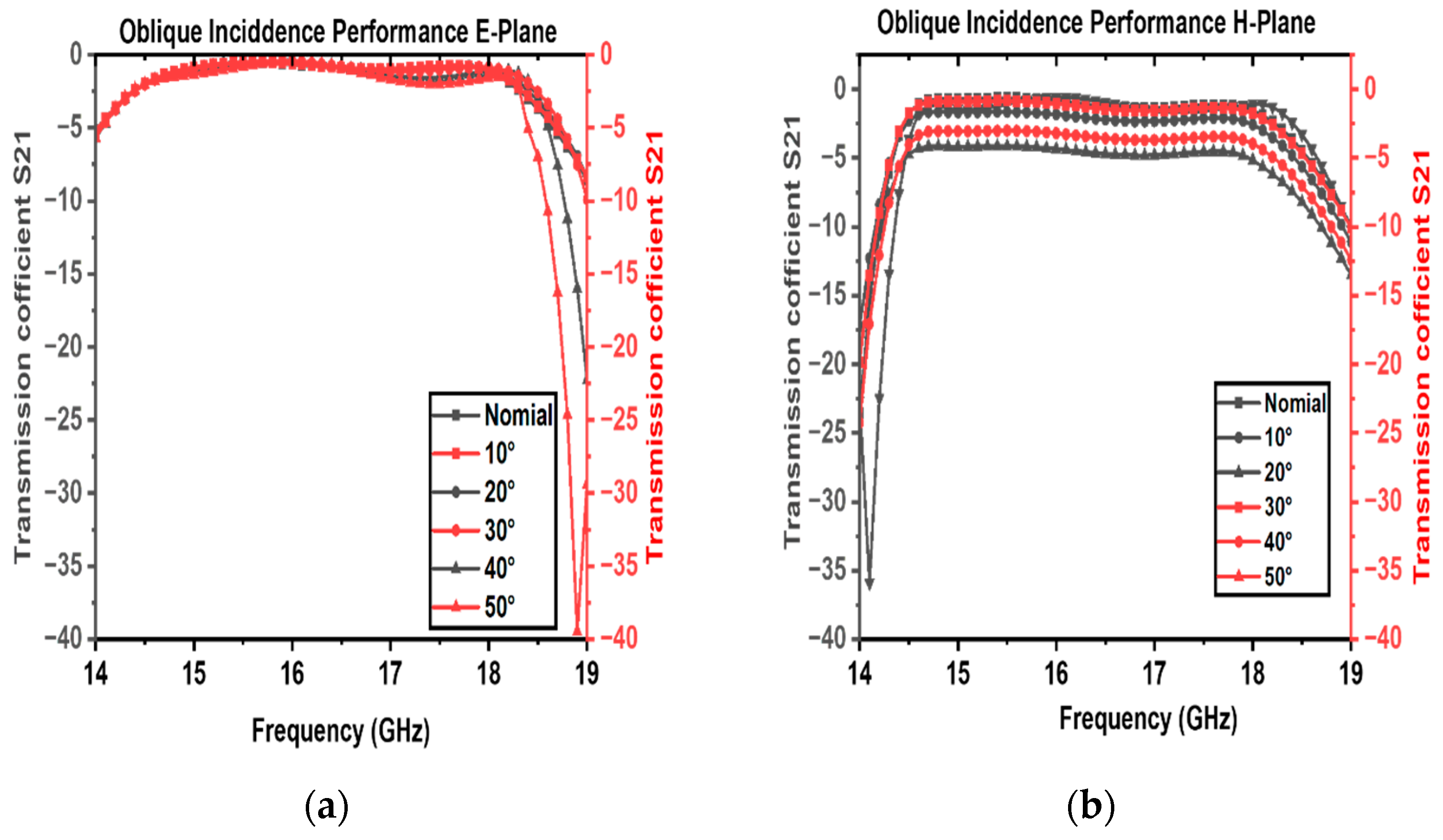
3.1. Oblique Incidence Performance
The oblique incidence performance was investigated in full-wave simulation under periodic boundary conditions. The Floquet port adds the top and bottom of the transmitter and receiver layers of the unit cell and the air box’s walls surrounded by the master/slave periodic boundary conditions on each incidence angle from 0 to 60 degrees. Scanning angles from 0 to 60 degrees with oblique incidences in
-plane and
-plane have been studied. The reflection and transmission coefficients oblique incidence performance from 0 to 60 degrees are shown in
Figure 5. The reflection coefficient S
for the transmitter layer (active patch) is less than −10 dB for each oblique incident angle.
The bandwidth shifted toward a higher frequency at 500 MHz; however, the bandwidth gets lower by 50–60 degrees and shifts toward the lower frequency at 16 GHz. The transmission coefficient increases with an increase in incidence, which is under −1 dB between 0 and 40 degrees, and the bandwidth of the unit cell increases on higher angles but enough for the central frequency at 16 GHz with low insertion losses. The H-plane oblique incidence performance to reflection coefficient S
of transmitter plane is under −10 dB until an angle of 40 degrees. It exceeded 50–60 degrees at an angle but was suitable along the center frequency. The transmission coefficient transmission loss exceeds as the angle of incidence increases, but it maintains less than −3 dB for 0–50 degrees. The insertion losses increase abruptly for 60 degrees is shown in
Figure 6.
3.2. Bias Lines
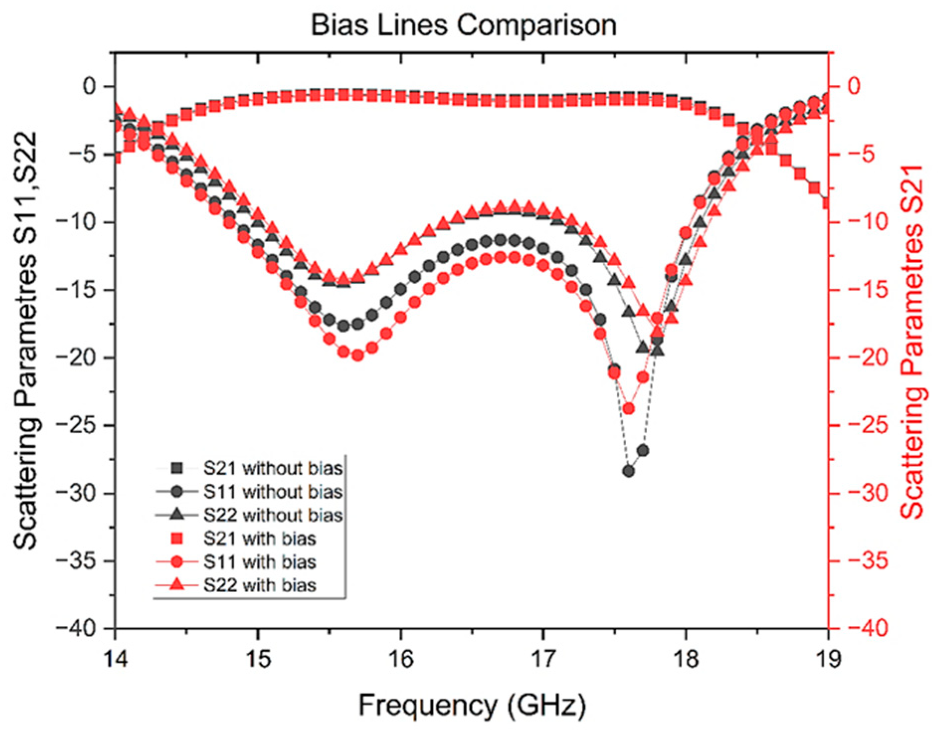
The proposed unit cell is the elementary unit of an immense transmitarray; it requires more bias lines to accommodate many unit cells, such as 10 bias lines (for 20 × 20 array) on each cell and 8 bias lines (for 16 × 16 array) on each unit cell transmitarray.
A simulation study was accomplished to understand the impact of bias lines on the unit cell and array structure results. The proposed unit cell is modified by adding ten bias lines into the unit cell in different configurations. Firstly, we added ten bias lines on the bonding film presented, five on the first bonding film, and five on the second bonding film. The simulation results are shown in
Figure 7. Consequently, the effect of bias line modification is negligible on the scattering parameters of the unit cell. This effect is due to the decoupling capacitive circuit, and parallel lines have a capacitive impact on the behavior of the unit cell. Bias lines also pass through the second bonding film in the second configuration; these are attached through metallic vias with decoupling capacitive plates. There is less impact on insertion losses due to bias lines; we add 10 bias lines on unit cell to analyze the effect of bias lines on whole array is shown in
Figure 8. The bias line has less impact so it is also has less impact on gain of the array that is no more than 0.2–0.3 dB approx.
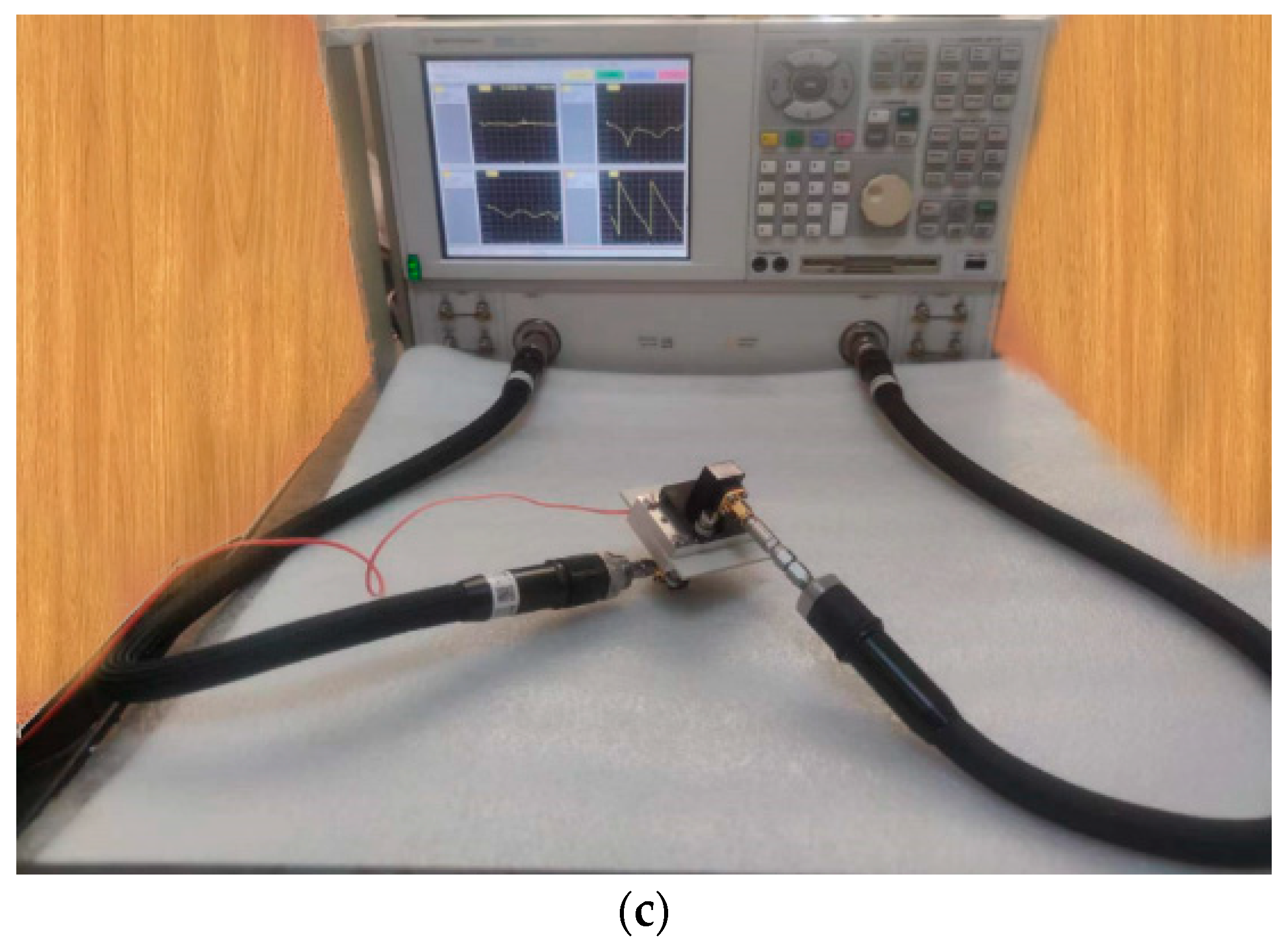
4. Measurement Results
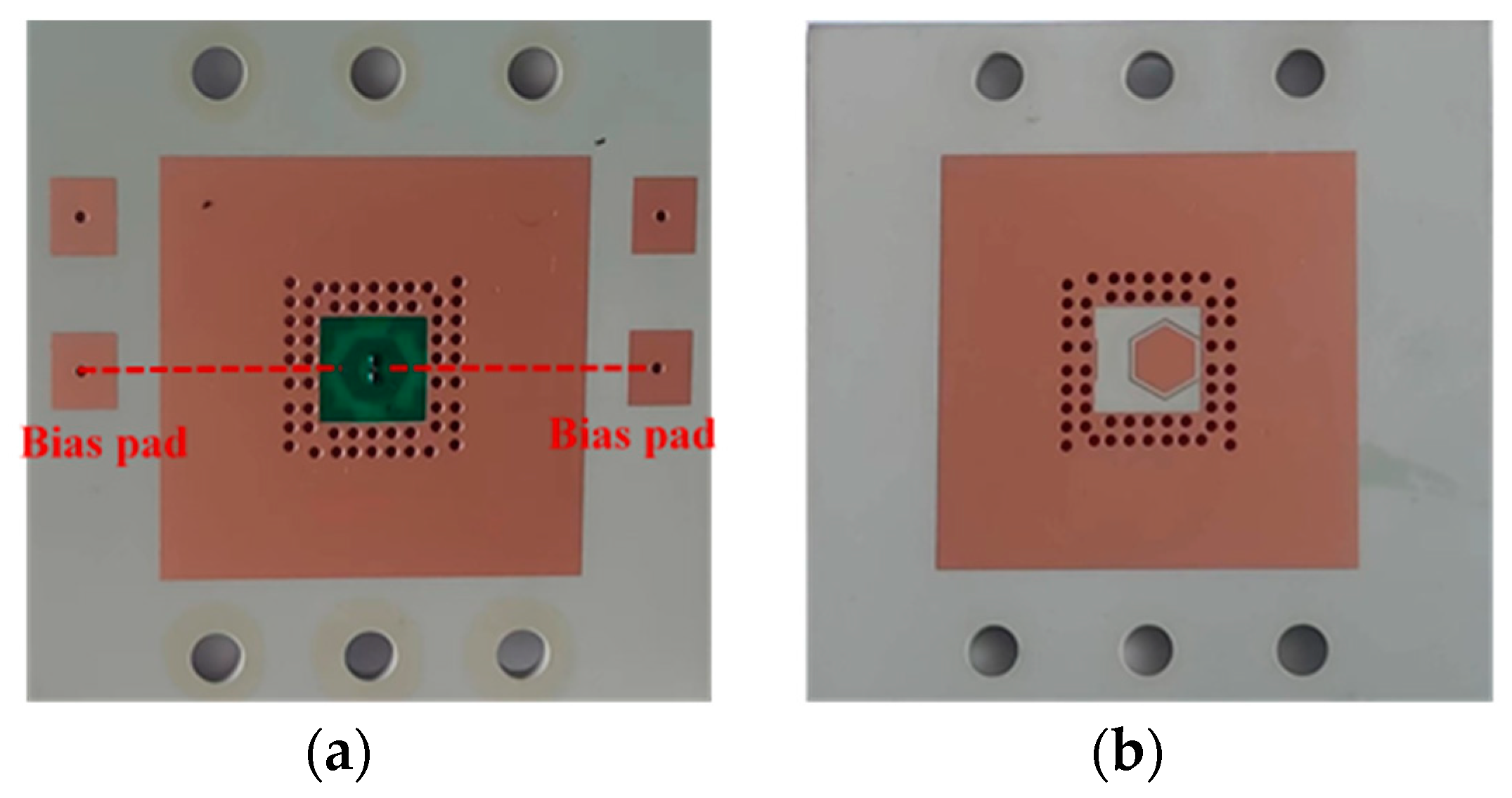
A fabricated unit cell is shown in
Figure 9 the actual unit cell is surrounded by square rings of 1 mm diameter metallic vias (
,
) to obtain electromagnetic connectivity between two WR62 waveguides through adopter conductors. The rectangular rings provide connectivity between the unit cell and the waveguide and help to avoid the different resonance modes of the substrate leaking out of the unit cell. There are two bias lines of width
mm that pass through the unit cell on both sides and end up with metallic pads to provide positive bias voltages to the PIN diodes. Two metallic lines with the same thickness are directly connected to the ground pass through the substrate, connected to the receiver structure, and end up on the ground pad at the top of the waveguide setup on the unit cell.
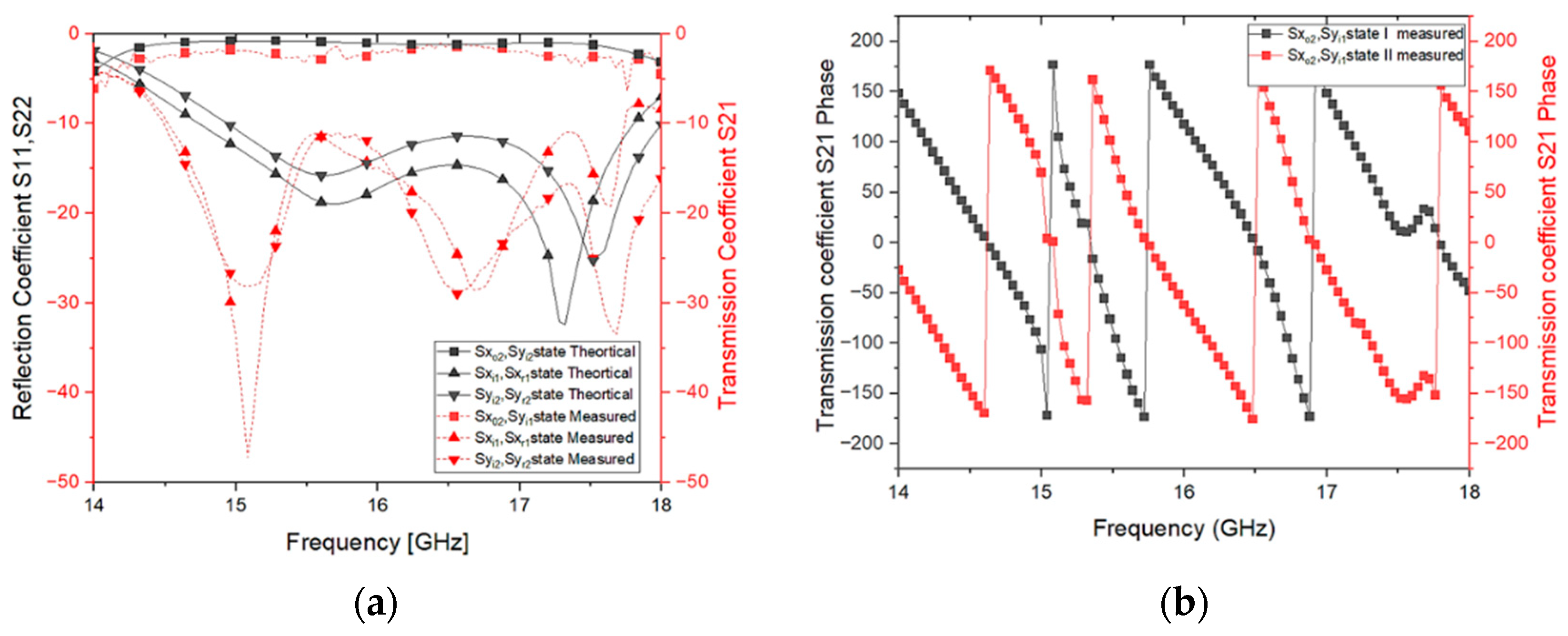
The measured 3 dB transmission bandwidth (S21) lies between 14.12 and 18.02 GHz with a minimum insertion loss of 1.12 dB and 1.14 dB for state I (0°) and state II (180°) at 16 GHz. The reconciliation between the simulated and measured results is promising. The differences between the measured and simulated results are less than 3 dB throughout the desired band for both phase states. The measured results are similar for phase state I and state II as the consequence of the symmetric current reversal technique adopted in the proposed unit cell.
There are fluctuations in the measured results because of the unstable behavior of the testing device and fabrication mismatch. The phase difference for both states are suitable for beam-scanning applications; the phase differences lie within 176–180 degrees. A complete comparison of the simulated and measured results is demonstrated below in
Figure 10a. The measured phase shift results are illustrated in
Figure 10b; the phase difference is stable with minor fluctuations and resonance on some points. The S
21 transmission phase difference observes that the minimum phase difference is not less than 176 degrees.
5. Design and Optimization of 20 × 20 Active Linearly Polarized Transmitarray for Ku Band
In this section, we have characterized the feasibility of a wideband and low-profile structure design array using the proposed one-bit wideband meander-shaped hexagonal unit cell structure. The proposed 20 × 20 transmitarray with a conventional method feed source is presented in
Figure 8. Each side of the array is 160 mm (8.8 × λ
o). The transmitarray has 400 PIN diodes to control the (0°/180°) phase distribution of the transmitted wave to achieve the desired radiation characteristics.
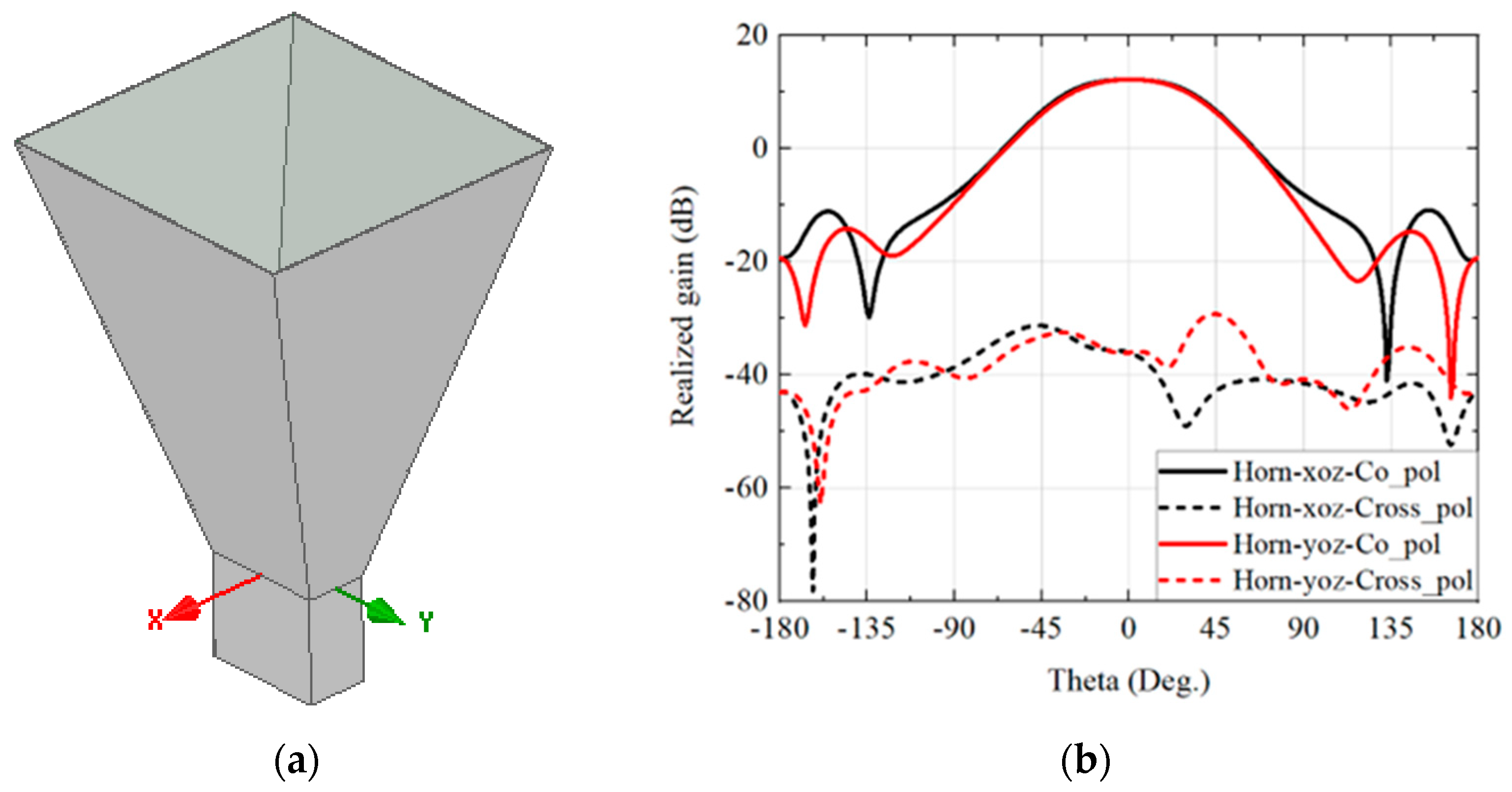
The structure diagram of the horn feed is shown in
Figure 11a and the size of the radiation port is 20 mm × 20 mm. The radiation pattern of the horn feeds at 16.5 GHz was obtained by the simulation shown in
Figure 11b. The half-power lobe widths corresponding to the two main planes are 69.96° and 66.2°, respectively; the Q of the horn was obtained by fitting it with MATLAB. The value is 1.8, and the calculated optimum focal diameter ratio is 0.54.
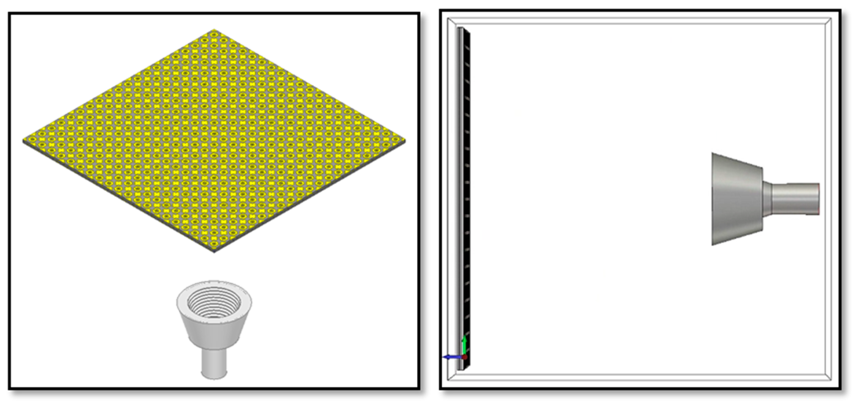
The performance of the TA was investigated on CST software for high-frequency simulation commercial tools. The array feed with a WR62 horn antenna with 10 dBi nominal gain located with focal distance, F = 112 mm (6.1λ
0, F/D = 0.7), was used and is illustrated in
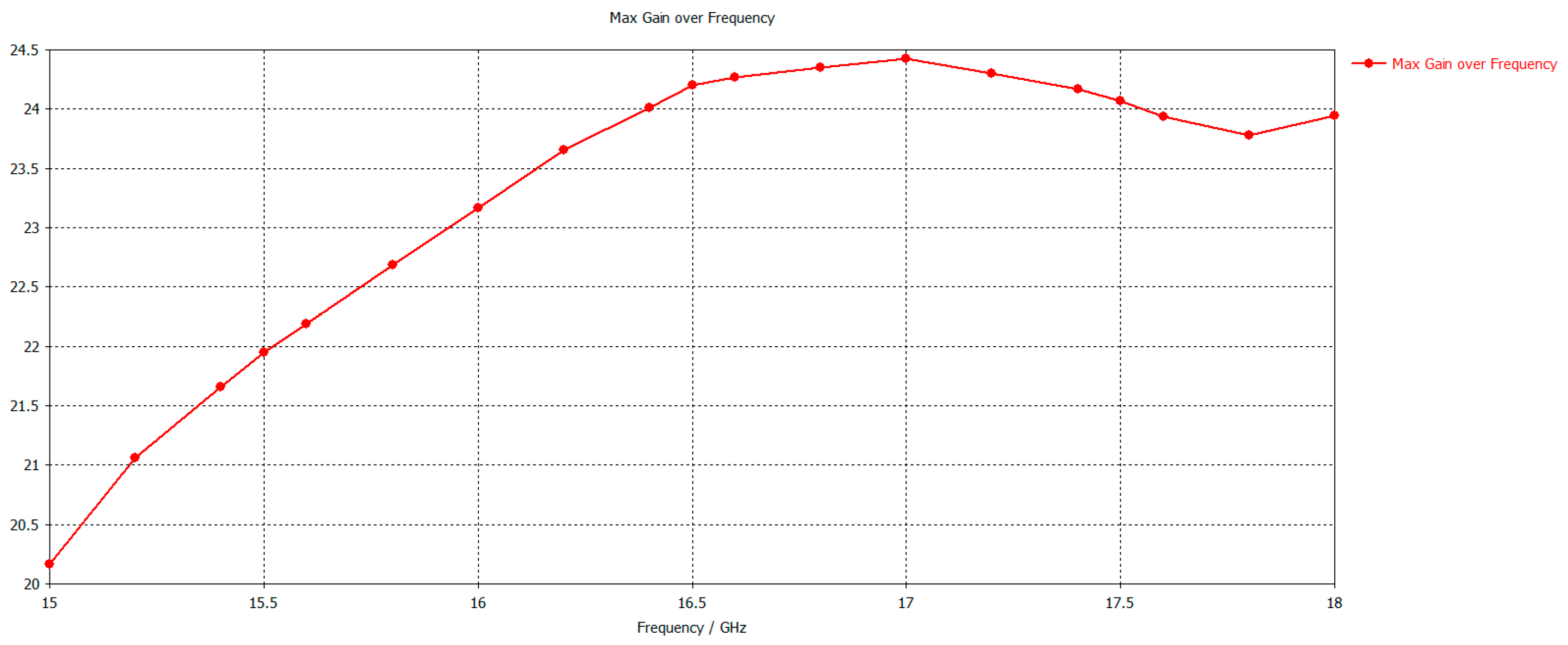
Figure 12. The 20 × 20 array max gain over frequency results are presented in
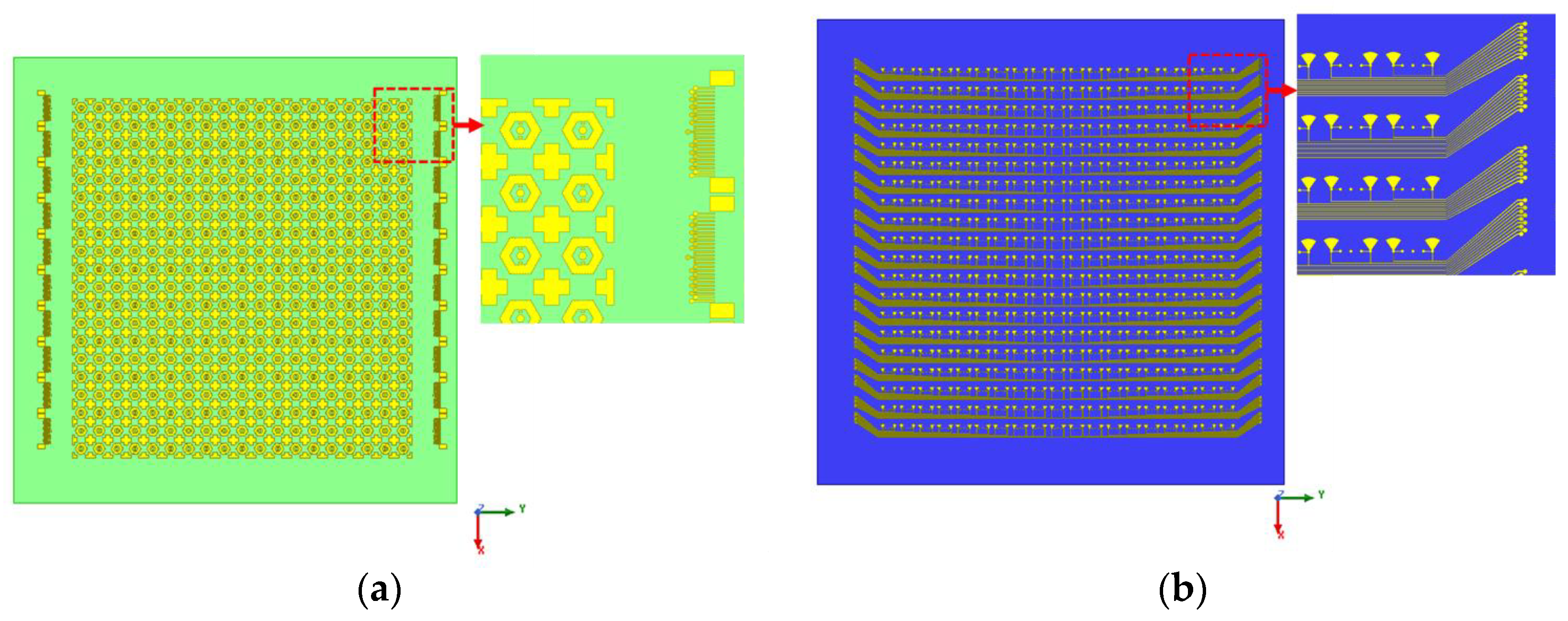
Figure 13. The 3 dB gain bandwidth results are stable from 15.3 to conward through out graph. The DC bias network layout of a one-bit reconfigurable transmitarray has been considered to obtain the independent control of each element in the transmitarray. The design uses surface mount connectors (24 pins) to control each transmitarray cell independently. The 24-pins connectors adopted in the entire bias line network are evenly distributed on the left- and right-hand sides of the surface of the transmit array. These details are illustrated in
Figure 14a,b with a complete fabrication scheme for the transmitarray. Metal through-holes connect each front surface mount connector pin with the corresponding bias line at the back.
The theoretical ad hoc simulator and full-wave simulation CST E-plane and H-plane radiation pattern are presented in
Figure 10. The higher side-lobe level (SLL) in the full-wave simulation is due to spillover radiation losses that are not part of the numerical simulations. The maximum gain is 24.4 dBi with a side-lobe level of −19.7 dB and an aperture efficiency of 74.4% at 16 GHz.
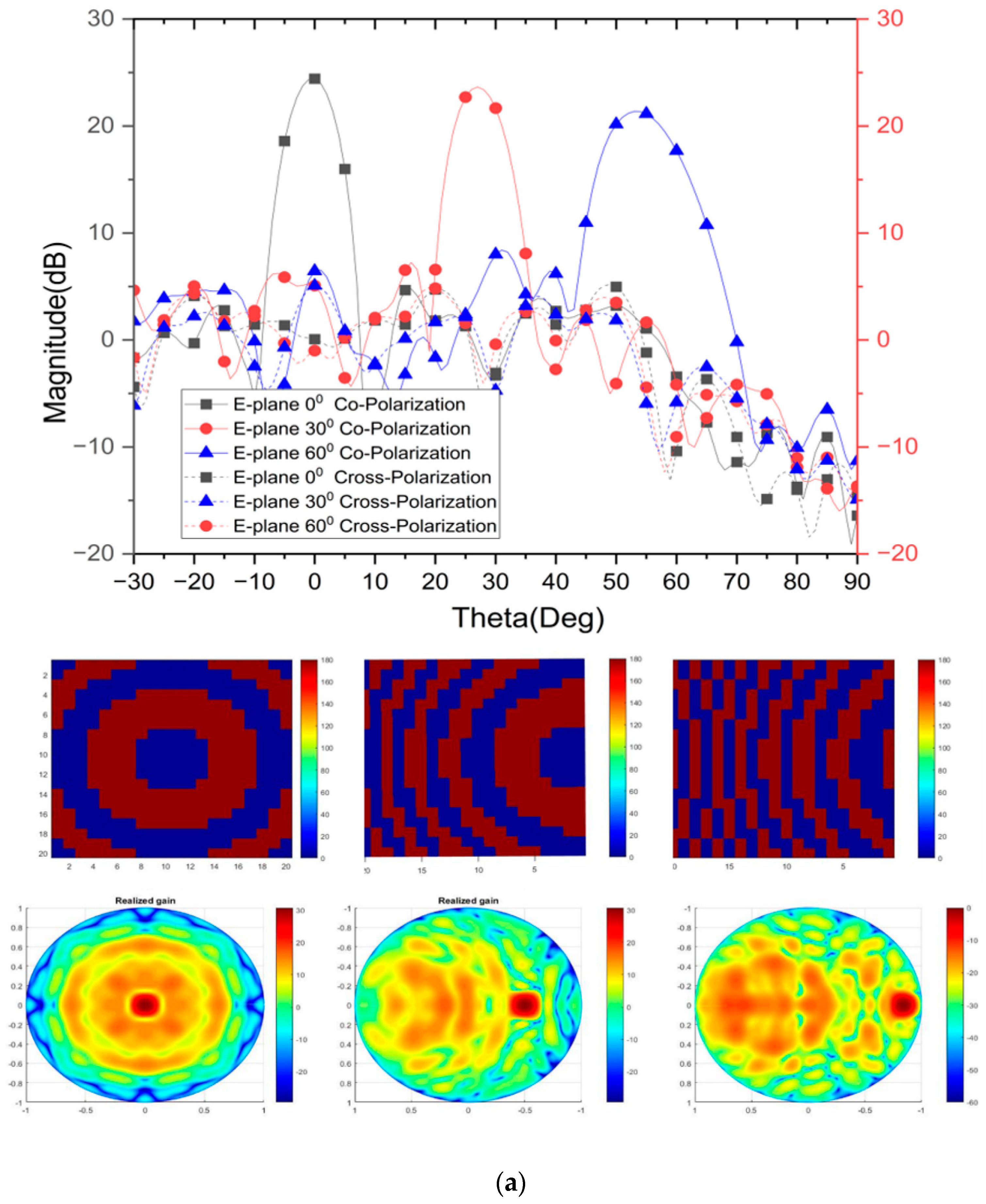
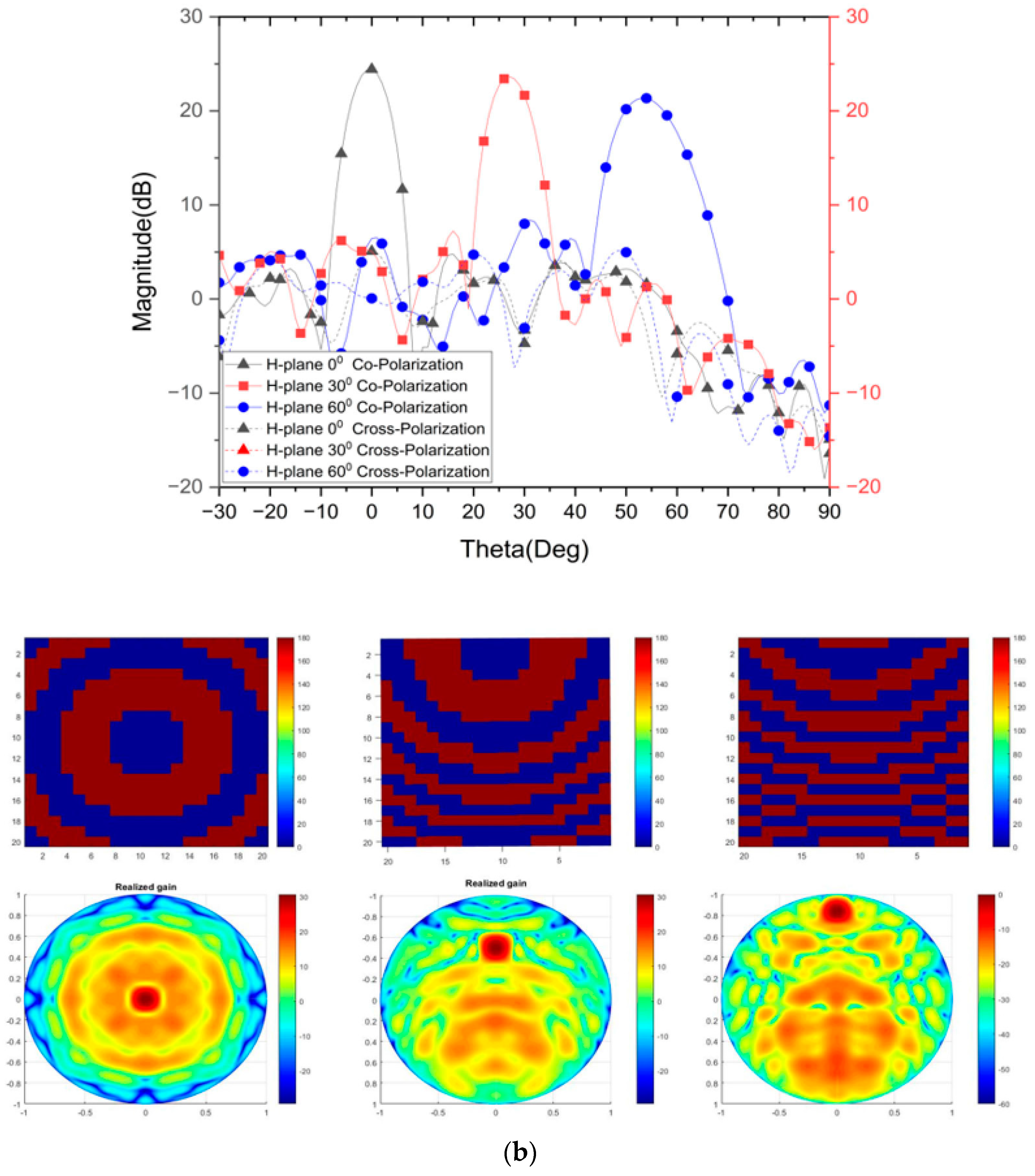
The results of the full-wave simulations to understand the array’s beam-scanning characteristics in the E-plane are presented in
Figure 15a,b at 16.5 GHz. The maximum gain reduces from 24.4 dBi to 20.8 dBi to a 60° scan angle. The simulated gain and directivity at 16.5 GHz are 24.4 dBi and 25.5i dB, respectively, for the 20 × 20 transmitarray. Thus, the radiation efficiency gain over the directivity ratio is 95.5%. The HPBW are 6.70 degrees and 6.76 degrees in the E plane and H plane, respectively. The side-lobe level (SLL) and cross-polarization level (CPL) are −19.7 dB and −22.4 dB, respectively. The aperture efficiency is obtained using the formula
where
which is approximately 29.1%. It is noted that the E-plane and H-plane radiation patterns are almost symmetrical due to the similar E- and H-plane oblique incidence performance of the unit cell.
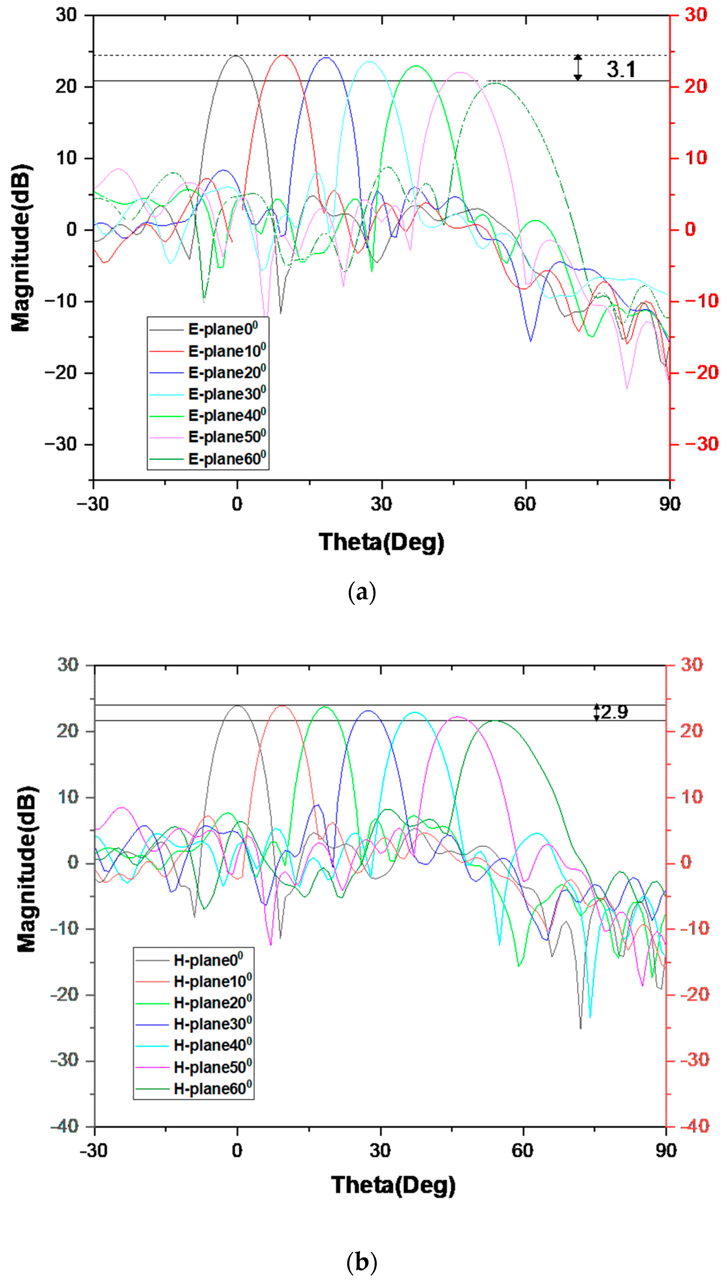
The phase distribution and focal distance (F) were selected for maximum aperture efficiency. Ad hoc simulator and full-wave simulations in CST compare the radiation patterns and characteristics of the reconfigurable transmitarray is shown in
Figure 16. The 3 dB gain bandwidth lies between 15 GHz and 18.6 GHz, associated with an overall fractional bandwidth of 19.18% at 16.5 GHz.
Several designs were investigated to reduce the one-bit phase quantization for two-bit or three-bit fixed beam (passive) transmitarrays. A 2-bit reconfigurable transmitarray requires at least 4 diodes to achieve a 90-degree phase shift for each phase state which makes a multi-bit design challenging in transmitarrays. It is not easy to control the reverse direction of the current in a unit cell by just applying all four diodes on the receiver or transmitter sides. Two diodes can be installed on the receiver side; on the other hand, two diodes can be installed on the transmitter side with different polarization. Four diodes are required for biasing two circuits to control the phase shift independently. The current reversal control of both sides provides us four states and can produce a two-bit reconfigurable transmitarray unit cell.


 ,
, 


